REV. C
Information furnished by Analog Devices is believed to be accurate and
reliable. However, no responsibility is assumed by Analog Devices for its
use, nor for any infringements of patents or other rights of third parties
which may result from its use. No license is granted by implication or
otherwise under any patent or patent rights of Analog Devices.
a
12-Bit High Speed Multiplying
D/A Converter
DAC312
© Analog Devices, Inc., 1996
One Technology Way, P.O. Box 9106, Norwood, MA 02062-9106, U.S.A.
Tel: 617/329-4700 Fax: 617/326-8703
FEATURES
Differential Nonlinearity: 61/2 LSB
Nonlinearity: 0.05%
Fast Settling Time: 250 ns
High Compliance: –5 V to +10 V
Differential Outputs: 0 to 4 mA
Guaranteed Monotonicity: 12 Bits
Low Full-Scale Tempco: 10 ppm/8C
Circuit Interface to TTL, CMOS, ECL, PMOS/NMOS
Low Power Consumption: 225 mW
Industry Standard AM6012 Pinout
Available In Die Form
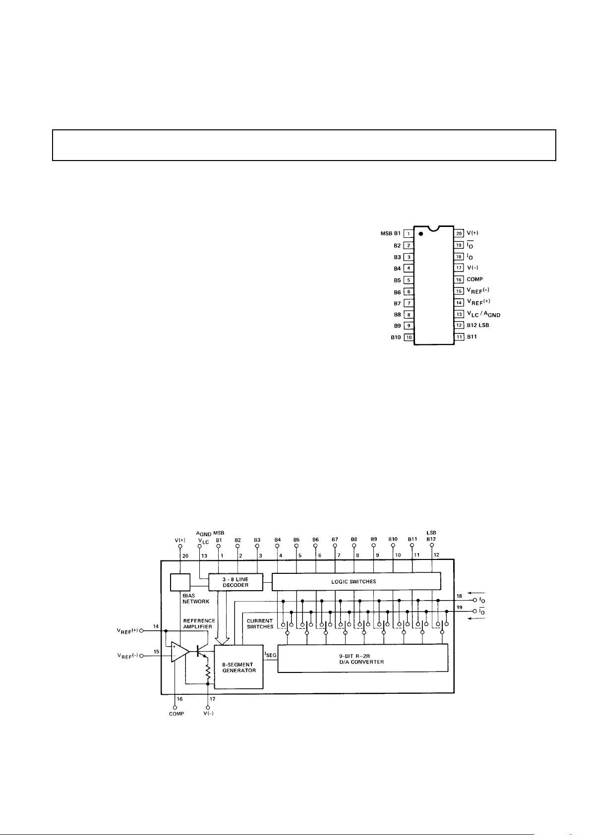
PIN CONNECTIONS
20-Pin Hermetic DIP (R-Suffix),
20-Pin Plastic DIP (P-Suffix),
20-Pin SOL (S-Suffix)
GENERAL DESCRIPTION
The DAC312 series of 12-bit multiplying digital-to-analog converters provide high speed with guaranteed performance to
0.012% differential nonlinearity over the full commercial operating temperature range.
The DAC312 combines a 9-bit master D/A converter with a
3-bit (MSBs) segment generator to form an accurate 12-bit D/A
converter at low cost. This technique guarantees a very uniform
step size (up to ±1/2 LSB from the ideal), monotonicity to
12-bits and integral nonlinearity to 0.05% at its differential current outputs. In order to provide the same performance with a
12-bit R-2R ladder design, an integral nonlinearity over temperature of 1/2 LSB (0.012%) would be required.
The 250 ns settling time with low glitch energy and low power
consumption are achieved by careful attention to the circuit design and stringent process controls. Direct interface with all
popular logic families is achieved through the logic threshold
terminal.
FUNCTIONAL BLOCK DIAGRAM
High compliance and low drift characteristics (as low as
10 ppm/°C) are also features of the DAC312 along with an excellent power supply rejection ratio of ± .001% FS/%∆V. Operating over a power supply range of +5/–11 V to ±18 V the
device consumes 225 mW at the lower supply voltages with an
absolute maximum dissipation of 375 mW at the higher supply
levels.
With their guaranteed specifications, single chip reliability and
low cost, the DAC312 device makes excellent building blocks
for A/D converters, data acquisition systems, video display drivers, programmable test equipment and other applications where
low power consumption and complete input/output versatility
are required.
DAC312N DAC312G
Parameter Symbol Conditions Typical Typical Units
Reference Input
Slew Rate dl/dt 8 8 mA/µs
Propagation Delay t
PLH
, t
PHL
Any Bit 25 25 ns
Settling Time t
S
To ±1/2 LSB, All
Bits Switched ON 250 250 ns
or OFF.
Full-Scale TC
IFS
±10 ±10 ppm/°C
REV. C
–2–
DAC312–SPECIFICA TIONS
ELECTRICAL CHARACTERISTICS
(@ VS = 615 V, I
REF
= 1.0 mA, 08C ≤ TA ≤ +708C for DAC312E and –408C ≤ TA ≤ +858C
for DAC312F, DAC312H, unless otherwise noted. Output characteristics refer
to both I
OUT
and I
OUT
.)
DAC312E DAC312F DAC312H
Parameter Symbol Conditions Min Typ Max Min Typ Max Min Typ Max Units
Resolution 12 12 12 Bits
Monotonicity 12 12 12 Bits
Differential Nonlinearity DNL Deviation from Ideal ±0.0125 ±0.0250 ±0.0250 %FS
Step Size
2
±0.5 ±1 ±1 LSB
Nonlinearity INL Deviation from Ideal ±0.05 ± 0.05 ± 0.05 %FS
Straight Line
1
Full-Scale Current I
FS
V
REF
= 10 V
R
14
= R
15
= 10 kΩ
2
3.967 3.999 4.031 3.935 3.999 4.063 3.935 3.999 4.063 mA
Full-Scale Tempco TCI
FS
± 5 ± 20 ±10 ±40 ±80 ppm/°C
± 0.005 ± 0.002 ±0.001 ± 0.004 ±0.008 %FS/°C
Output Voltage Compliance V
OC
DNL Specification Guaranteed over Compliance Range –5 +10 –5 +10 –5 +10 V
Full-Scale Symmetry I
FSS
|IFS|–|IFS| ± 0.4 ± 1 ±0.4 ±2 ± 0.4 ± 2 µA
Zero-Scale Current I
ZS
0.10 0.10 0.10 µA
Settling Time t
S
To ± 1/2 LSB, All Bits
Switched ON or OFF
1
250 500 250 500 250 500 ns
Propagation Delay–All Bits t
PLH
All Bits Switched 50% Point 25 50 25 50 25 50 ns
t
PHL
Logic Swing to 50% Point 25 50 25 50 25 50 ns
Output
1
Output Resistance R
O
>10 >10 >10 MΩ
Output Capacitance C
OUT
20 20 20 pF
Logic Input
Levels “0” V
IL
V
LC
= GND 0.8 0.8 0.8 V
Levels “1” V
IH
VLC = GND 2 2 2 V
Logic Input Current I
IN
VIN = –5 to +18 V 40 40 40 µA
Logic Input Swing V
IS
–5 +18 –5 +18 –5 +18 V
Reference Bias Current I
15
0 –0.5 –2 0 –0.5 –2 0 –0.5 –2 µA
Reference Input
Slew Rate dl/dt R
14(eq)
= 800 Ω, CC = 0 pF14 8 48 48 mA/µs
Power Supply Sensitivity PSSI
FS+
V+ = +13.5 V to +16.5 V,
V– = –15 V ±0.0005 ±0.001 ±0.0005 ± 0.001 ± 0.0005 ±0.001 %FS/%∆V
PSSI
FS–
V– = –13.5 V to –16.5 V,
V+ = +15 V ±0.00025 ±0.001 ±0.00025 ±0.001 ±0.00025 ±0.001 %FS/%∆V
Power Supply Range V+ V
OUT
= 0 V 4.5 18 4.5 18 4.5 18 V
V– V
OUT
= 0 V –18 –10.8 –18 –10.8 –18 –10.8 V
Power Supply Current I+ V+ = +5 V, V– = –15 V 3.3 7 3.3 7 3.3 7 mA
I– V+ = +15 V, V– = –15 V –13.9 –18 –13.9 –18 –13 9 –18 mA
I+ V+ = +5 V, V– = –15 V 3.9 7 3.9 7 3.9 7 mA
I– V+ = +15 V, V– = –15 V –13.9 –18 –13.9 –18 –13.9 –18 mA
Power Dissipation P
d
V+ = +5 V, V– = –15 V 225 305 225 305 225 305 mW
V+ = +15 V, V– = –15 V 267 375 267 375 267 375 mW
TYPICAL ELECTRICAL CHARACTERISTICS
@ 258C; VS = 615 V, and I
REF
= 1.0 mA, unless otherwise noted. Output
characteristics refer to both I
OUT
and I
OUT
.

ELECTRICAL CHARACTERISTICS
DAC312E DAC312F DAC312H
Parameter Symbol Conditions Min Typ Max Min Typ Max Min Typ Max Units
Logic Input
Levels “0” V
IL
V
LC
= GND 0.8 0.8 0.8 V
Logic Input
Levels “1” V
IH
VLC = GND 2 2 2 V
Logic Input
Current I
IN
VIN = –5 V to +18 V 40 40 40 µA
Logic Input
Swing V
IS
–5 +18 –5 +18 –5 +18 V
Reference Bias
Current I
15
0 –0.5 –2 0 –0.5 –2 0 –0.5 –2 µA
Reference Input dl/dt R
14(eq)
= 800 Ω 4 8 4 8 4 8 mA/µs
Slew Rate CC = 0 pF (Note 1)
V+ = +13.5 V to +16.5 V, ±0.0005 ±0.001 ±0.0005 ± 0.001 ±0.0005 ±0.001 %FS/%∆V
Power Supply PSSI
FS+
V– = –15 V
Sensitivity PSSI
FS–
V– = –13.5 V to –16.5 V, ±0.00025 ±0.001 ±0.00025 ±0.001 ±0.00025 ±0.001 %FS/%∆V
V+ = +15 V
Power Supply V+ 4.5 18 4.5 18 4.5 18
Range V– V
OUT
= 0 V –18 –10.8 –18 –10.8 –18 –10.8 V
I+ 3.3 7 3.3 7 3.3 7
Power Supply I– V+ = +5 V, V– = –15 V –13.9 –18 –13.9 –18 –13.9 –18
Current I+ V+ = +15 V, V– = –15 V 3.9 7 3.9 7 3.9 7 mA
I– –13.9 –18 –13.9 –18 –13.9 –18
Power V+ = +5 V, V– = –15 V 225 305 225 305 225 305
Dissipation P
d
V+ = +15 V, V– = –15 V 267 375 267 375 267 375 mW
NOTES
1
Guaranteed by design.
2
TA = +25°C for DAC312H grade only.
Specifications subject to change without notice.
@ VS = 615 V, I
REF
= 1.0 mA, 08C ≤ TA ≤ 708C for DAC312E and –408C ≤ TA ≤ +858C for
DAC312F, DAC312H, unless otherwise noted. Output characteristics refer to both I
OUT
and I
OUT
.
Continued
–3–
REV. C
DAC312
DAC312
–4–
REV. C
WAFER TEST LIMITS
DAC312N DAC312G
Parameter Symbol Conditions Limit Limit Units
Resolution 12 12 Bits min
Monotonicity 12 12 Bits min
Nonlinearity ±0.05 ± 0.05 %FS max
Output Voltage Full-Scale Current +10 +10 V max
Compliance Voc Change <1/2 LSB –5 –5 V min
Full-Scale V
REF
= 10.000 V 4.031 4.063 mA max
Current R14, R15 = 10.000 kΩ 3.967 3.935 mA min
Full-Scale Symmetry I
FSS
±1 ±2 µA max
Zero-Scale Current I
ZS
0.1 0.1 µA max
Differential DNL Deviation from ±0.012 ±0.025 %FS max
Nonlinearity Ideal Step Size ±1/2 ±1 Bits (LSB) max
Logic Input Levels “0” V
IL
VLC = GND 0.8 0.8 V max
Logic Input Levels “1” V
IH
VLC = GND 2 2 V min
Logic Input Swing V
IS
+18 +18 V max
–5 –5 V min
Reference Bias
Current I
15
–2 –2 µA max
Power Supply PSSI
FS+
V+ = +13.5 V to +16.5 V, V– = –15 V ±0.001 ±0.001
Sensitivity PSSI
FS–
V– = –13.5 V to –16.5 V, V+ = +15 V ±0.001 ±0.001 %/%max
Power Supply I+ V
S
= +15 V 7 7
Current I– I
REF
≤ 1.0 mA –18 –18 mA max
Power V
S
= +15 V
Dissipation P
D
I
REF
≤ 1.0 mA 375 375 mW max
NOTE
Electrical tests are performed at wafer probe to the limits shown. Due to variations in assembly methods and normal yield loss, yield after packaging is not guaranteed
for standard product dice. Consult factory to negotiate specifications based on dice lot qualification through sample lot assembly and testing.
@ VS = 615 V, I
REF
= 1.0 mA, TA = 258C, unless otherwise noted. Output characteristics refer to both I
OUT
and I
OUT
.
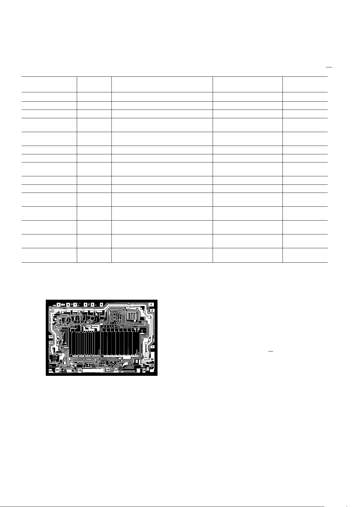
DICE CHARACTERISTICS
DIE SIZE 0.141 × 0.096 inch, 13,536 sq. mils (3.58 × 2.44 mm, 8.74 sq. mm)
1. B1 (MSB) 11. B11
2. B2 12. B12 (LSB)
3. B3 13. V
LC/AGND
4. B4 14. V
REF
(+)
5. B5 15. V
REF
(–)
6. B6 16. COMP
7. B7 17. V–
8. B8 18. I
O
9. B9 19. I
O
10. B10 20. V+
DAC312
–5–
REV. C
ORDERING GUIDE
1
Temperature Package Package
Model DNL Range Description Option
DAC312ER2±1/2 LSB 0°C to +70°C Cerdip-20 Q-20
DAC312FR ±1 LSB –40°C to +85°C Cerdip-20 Q-20
DAC312BR/883 ± 1 LSB –55°C to +125°C Cerdip-20 Q-20
DAC312HP ± 1 LSB –40°C to +85°C Plastic DIP-20 N-20
DAC312HS ± 1 LSB –40°C to +85°C SOL-20 R-20
NOTES
1
Burn-in is available on commercial and industrial temperature range parts in
cerdip, plastic DIP, and TO-can packages.
2
For devices processed in total compliance to MIL-STD-883, add/883 after part
number. Consult factory for 883 data sheet.
ABSOLUTE MAXIMUM RATINGS
1
Operating Temperature
DAC312E . . . . . . . . . . . . . . . . . . . . . . . . . . . . . . 0°C to +70°C
DAC312F, DAC312H . . . . . . . . . . . . . . . . . . –40°C to +85°C
Junction Temperature . . . . . . . . . . . . . . . . . . . . –65°C to +150°C
Storage Temperature (Tj) . . . . . . . . . . . . . . . . . –65°C to +125°C
Lead Temperature (Soldering, 60 sec) . . . . . . . . . . . . . . . .300°C
Power Supply Voltage . . . . . . . . . . . . . . . . . . . . . . . . . . . . .±18 V
Logic Inputs . . . . . . . . . . . . . . . . . . . . . . . . . . . . . –5 V to +18 V
Analog Current Outputs . . . . . . . . . . . . . . . . . . . . –8 V to +12 V
Reference Inputs V
14
, V15 . . . . . . . . . . . . . . . . . . . . . . . V– to V+
Reference Input Differential Voltage (V
14
, V15) . . . . . . . . . . ±18 V
Reference Input Current (I
14
) . . . . . . . . . . . . . . . . . . . . . 1.25 mA
Package Type u
JA
2
u
JC
Units
20-Pin Hermetic DIP (R) 76 11 °C/W
20-Pin Plastic DIP (P) 69 27 °C/W
20-Pin SOL (S) 88 25 °C/W
NOTES
1
Absolute maximum ratings apply to both DICE and packaged parts, unless
otherwise noted.
2
θJA is specified for worst case mounting conditions, i.e., θJA is specified for device
in socket for cerdip and P-DIP packages; θJA is specified for device soldered to
printed circuit board for SOL package.
WARNING!
ESD SENSITIVE DEVICE
CAUTION
ESD (electrostatic discharge) sensitive device. Electrostatic charges as high as 4000 V readily
accumulate on the human body and test equipment and can discharge without detection.
Although the DAC312 features proprietary ESD protection circuitry, permanent damage may
occur on devices subjected to high energy electrostatic discharges. Therefore, proper ESD
precautions are recommended to avoid performance degradation or loss of functionality.
 Loading...