16-Bit High Speed
SETTLING TIME – ns
0.1
0.01
0.001
0 100
PERCENT OF FULL-SCALE – %
200 300 400 500 600 700 800
V
LOGIC
= 0V
TURNING ON
V
LOGIC
= +5V
TURNING OFF
I
FS
= 4mA
T
A
= 258C
a
FEATURES
ⴞ1 LSB Differential Linearity (max)
Guaranteed Monotonic Over Temperature Range
ⴞ2 LSB Integral Linearity (max)
500 ns Settling Time
5 mA Full-Scale Output
TTL/CMOS Compatible
Low Power: 190 mW (typ)
Available in Die Form
APPLICATIONS
Communications
ATE
Data Acquisition Systems
High Resolution Displays
GENERAL DESCRIPTION
The DAC16 is a 16-bit high speed current-output digital-toanalog converter with a settling time of 500 ns. A unique combination of low distortion, high signal-to-noise ratio, and high
speed make the DAC16 ideally suited to performing waveform
synthesis and modulation in communications, instrumentation,
and ATE systems. Input reference current is buffered, with fullscale output current of 5 mA. The 16-bit parallel digital input
bus is TTL/CMOS compatible. Operating from +5 V and
–15 V supplies, the DAC16 consumes 190 mW (typ) and is
available in a 24-lead epoxy DIP, epoxy surface-mount small
outline (SOL), and in die form.
Current-Output DAC
FUNCTIONAL BLOCK DIAGRAM
I
REF
REF GND
V
AGND
V
DGND
BUFFER
CC
EE
DB0 (LSB)
DAC16
DAC
DB15 (MSB)
DAC16
C
COMP
I
OUT
REV. B
Information furnished by Analog Devices is believed to be accurate and
reliable. However, no responsibility is assumed by Analog Devices for its
use, nor for any infringements of patents or other rights of third parties
which may result from its use. No license is granted by implication or
otherwise under any patent or patent rights of Analog Devices.
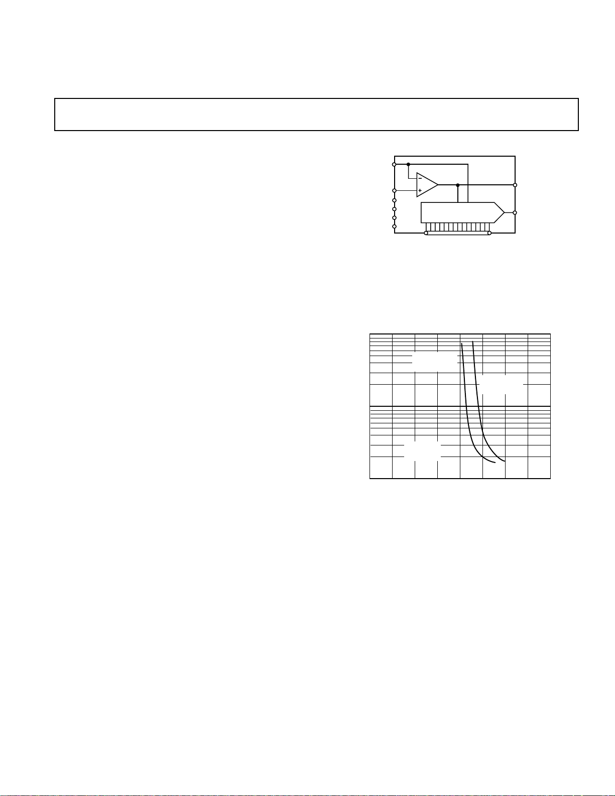
Figure 1. DAC16 Settling Time Accuracy vs. Percent of
Full Scale
One Technology Way, P.O. Box 9106, Norwood, MA 02062-9106, U.S.A.
Tel: 781/329-4700 World Wide Web Site: http://www.analog.com
Fax: 781/326-8703 © Analog Devices, Inc., 1999

DAC16–SPECIFICATIONS
(@ VCC = +5.0 V, VEE = –15.0 V, I
ELECTRICAL CHARACTERISTICS
Parameter Conditions Min Typ Max Units
perature Range unless otherwise noted. See Note 1 for supply variations.)
= 0.5 mA, C
REF
= 47 F, TA = Full Operating Tem-
COMP
Integral Linearity “G” INL T
= +25°C–2±1.2 +2 LSB
A
Integral Linearity “G” INL –4 ±1.6 +4 LSB
Differential Linearity “G” DNL T
= +25°C–1±0.5 +1 LSB
A
Differential Linearity “G” DNL –1 ±0.7 +1.5 LSB
Integral Linearity “F” INL T
= +25°C–4±1.4 +4 LSB
A
Integral Linearity “F” INL –6 ±2 +6 LSB
Differential Linearity “F” DNL T
= +25°C–1±0.5 +1.5 LSB
A
Differential Linearity “F” DNL –1.5 ±0.6 +2 LSB
Zero Scale Error ZSE 1 LSB
Zero Scale Drift TC
ZSE
0.025 ppm/°C
Gain Error GE ±0.225 % FS
Gain Drift TC
REFERENCE
Reference Input Current I
2
REF
GE
Note 2 350 625 µA
5 ppm/°C
OUTPUT CHARACTERISTICS
Output Current I
Output Capacitance C
Settling Time t
OUT
S
Note 2 2.8 5.0 mA
OUT
10 pF
0.003% of Full Scale 500 ns
LOGIC CHARACTERISTICS
T
Logic Input High Voltage V
Logic Input Low Voltage V
Logic Input Current I
Logic Input Current I
Logic Input Current I
Input Capacitance C
INH
INL
INH
INH
INL
IN
= +25°C 2.4 V
A
T
= +25°C 0.8 V
A
V
= 5.0 V, DB0–DB10 7.5 µA
IN
V
= 5.0 V, DB11–DB15 100 µA
IN
V
= 0 V, DB0–DB15 1 µA
IN
8pF
SUPPLY CHARACTERISTICS
Power Supply Sensitivity PSS V
Positive Supply Current I
Positive Supply Current I
Negative Supply Current I
Power Dissipation P
NOTES
1
All supplies can be varied ±5% and operation is guaranteed. Device is tested with nominal supplies.
2
Operation is guaranteed over this reference range, but linearity is neither tested not guaranteed (see Figures 7 and 8).
Specifications subject to change without notice.
CC
CC
EE
DISS
= 4.5 V to 5.5 V, VEE = –13 V to –17 V 20 ppm/V
CC
All Bits HIGH 15 22 mA
All Bits LOW 6 7.5 mA
7.5 10 mA
188 260 mW
WAFER TEST LIMITS
(@ VCC = +5.0 V, VEE = –15.0 V, I
= 0.5 mA, C
REF
= 47 F, TA = +25ⴗC unless otherwise noted.)
COMP
DAC16G
Parameter Symbol Conditions Limit Units
Integral Nonlinearity INL ±3 LSB max
Differential Nonlinearity DNL ±1 LSB max
Zero Scale Error ZSE ±1 LSB max
Gain Error GE ±12 % FS max
Logic Input High Voltage V
Logic Input Low Voltage V
Logic Input Current I
Positive Supply Current I
Negative Supply Current I
Power Dissipation P
NOTE
Electrical tests are performed at wafer probe to the limits shown. Due to variations in assembly methods and normal yield loss, yield after packaging is not guaranteed
for standard product dice. Consult factory to negotiate specifications based on dice lot qualification through sample lot assembly and testing.
INH
INL
IN
CC
EE
DISS
–2–
2.4 V min
0.8 V max
75 µA max
20 mA max
10 mA max
250 mW max
REV. B

DAC16
ABSOLUTE MAXIMUM RATINGS
(T
= +25°C unless otherwise noted)
A
VCC to VEE . . . . . . . . . . . . . . . . . . . . . . . . . . . –0.3 V, +25.0 V
V
to DGND . . . . . . . . . . . . . . . . . . . . . . . . . –0.3 V, +7.0 V
CC
V
to AGND . . . . . . . . . . . . . . . . . . . . . . . . +0.3 V, –18.0 V
EE
DGND to AGND . . . . . . . . . . . . . . . . . . . . . . –0.3 V, +0.3 V
REF GND to AGND . . . . . . . . . . . . . . . . . . . –0.3 V, +1.0 V
. . . . . . . . . . . . . . . . . . . . . . . . . . . . . . . . . . . . . . . . . 1 mA
I
REF
Analog Output Current . . . . . . . . . . . . . . . . . . . . . . . . . . 8 mA
Digital Input Voltage to DGND . . . . . . . . . . . . . . . . . . . ≤V
CC
Operating Temperature Range
FP, FS . . . . . . . . . . . . . . . . . . . . . . . . . . . . –40°C to +85°C
GS . . . . . . . . . . . . . . . . . . . . . . . . . . . . . . . . . 0°C to +70°C
Dice Junction Temperature . . . . . . . . . . . . . . . . . . . . . +150°C
Storage Temperature . . . . . . . . . . . . . . . . . . –65°C to +150°C
Power Dissipation . . . . . . . . . . . . . . . . . . . . . . . . . . 1000 mW
Lead Temperature (Soldering, 60 sec) . . . . . . . . . . . . +300°C
Package Type θ
1
JA
θ
JC
Units
24-Lead Plastic DIP (P) 62 32 °C/W
24-Lead Plastic SOL (S) 70 22 °C/W
NOTE
1
θJA is specified for worst case mounting conditions, i.e., θ
device in socket.
is specified for
JA
DICE CHARACTERISTICS
VCCDGND I
DB15 (MSB)
DB14
DB13
DB12
DB11
DB10
REF
C
COMP
I
OUT
AGND
DB4DB5DB6DB7DB8DB9
REF GND
V
EE
DB0 (LSB)
DB1
DB2
DB3
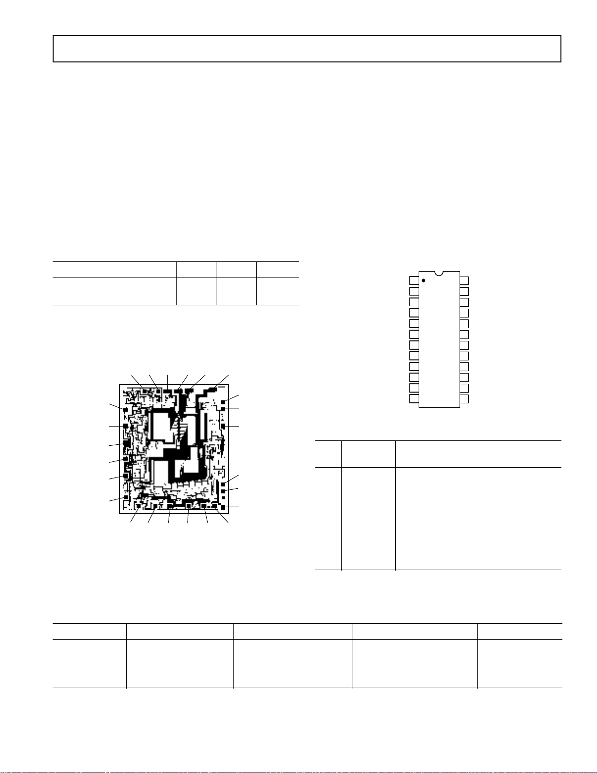
Die Size 0.129 x 0.153 inch, 19,737 sq. mils
(3.277 x 3.886 mm, 12.73 sq. mm)
The DAC16 Contains 330 Transistors.
Substrate is V
Polarity.
EE
CAUTION
1. Stresses above those listed under “Absolute Maximum Ratings” may cause permanent damage to the device. This is a
stress rating only and functional operation at or above this
specification is not implied. Exposure to the above maximum
rating conditions for extended periods may affect device
reliability.
2. Digital inputs and outputs are protected; however, permanent damage may occur on unprotected units from high energy electrostatic fields. Keep units in conductive foam or
packaging at all times until ready to use. Use proper antistatic handling procedures.
3. Remove power before inserting or removing units from their
sockets.
PIN CONFIGURATION
24-Lead DIP (P, S)
I
REF
DGND
V
DB15 (MSB)
DB14
DB13
DB12
DB11
DB10
DB9
DB8
DB7
CC
1
2
3
4
5
DAC16
6
TOP VIEW
(Not to Scale)
7
8
9
10
11
12
24
C
23
I
22
AGND
21
REF GND
20
V
19
DB0 (LSB)
18
DB1
17
DB2
16
DB3
15
DB4
14
DB5
13
DB6
COMP
OUT
EE
PIN DESCRIPTION
Pin
(P, S) Name Description
1I
REF
Reference Current Input
2 DGND Digital Ground
3V
CC
+5 V Digital Supply
4–19 DB15–DB0 16-Bit Digital Input Bus. DB15 is the MSB.
20 V
EE
–15 V Analog Supply
21 REF GND Reference Current Return
22 AGND Analog Ground/Output Reference
23 I
24 C
OUT
COMP
Current Output
Current Ladder Compensation
ORDERING GUIDE
Model Grade DNL (max) Temperature Ranges Package Descriptions Package Options
DAC16GS ±10°C to +70°C 24-Lead SOL R-24
DAC16FP ±2 –40°C to +85°C 24-Lead PDIP N-24
DAC16FS ±2 –40°C to +85°C 24-Lead SOL R-24
DAC16GBC ±1 +25°CDie
REV. B
–3–

DAC16
+5V
10kV
1
2
3
4
5
6
7
8
9
10
11
12
24
NC
23
22
21
20
19
18
17
16
15
14
13
–15V
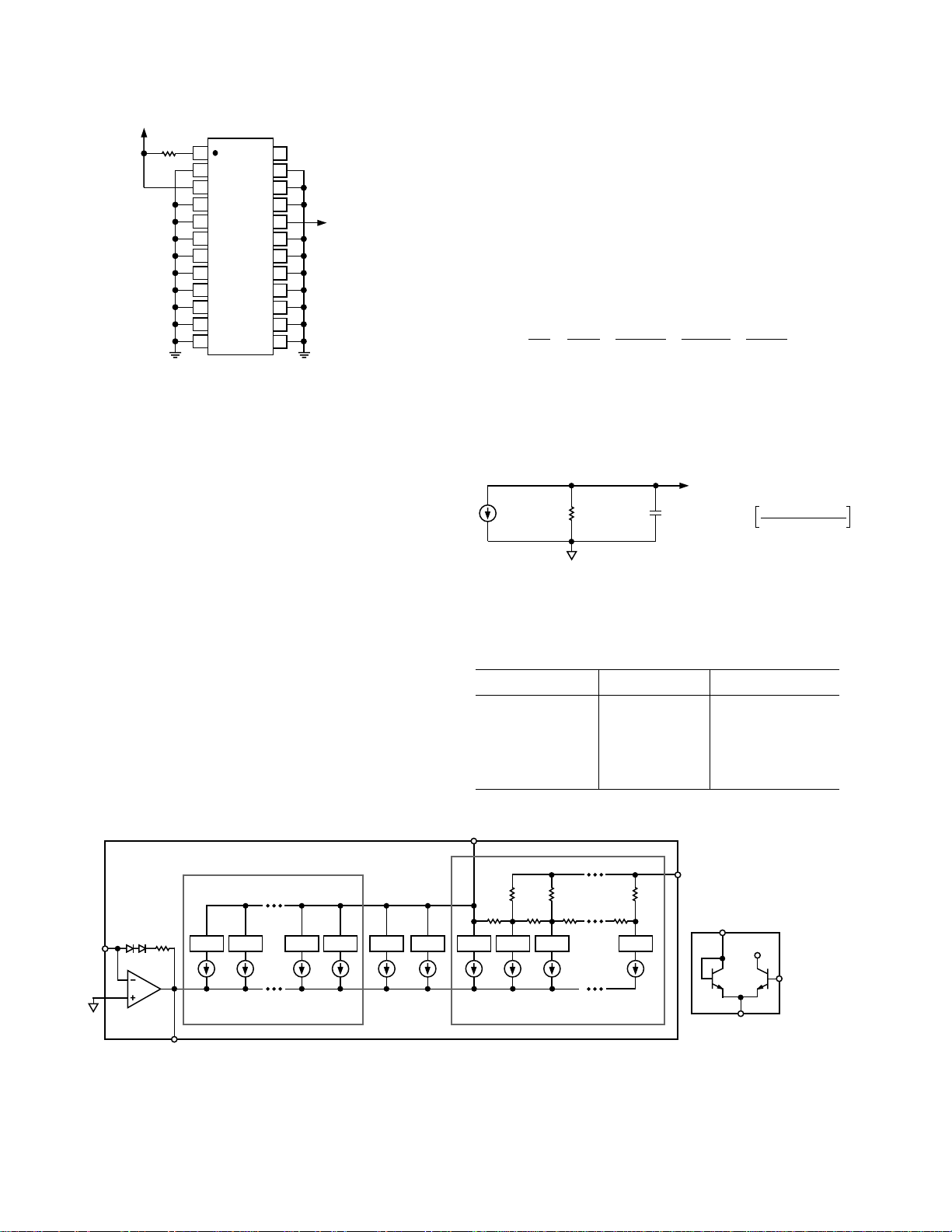
Figure 2. Burn-In Diagram
OPERATION
Novel DAC Architecture
The DAC16 was designed with a compound DAC architecture
to achieve high accuracy, excellent linearity, and low transition
errors. As shown in Figure 3, the DAC’s five most-significant
bits utilize 31 identical segmented current sources to obtain
optimal high speed settling at major code transitions. The lower
nine bits utilize an inverted R-2R ladder network which is lasertrimmed to ensure excellent differential nonlinearity. The middle
two bits (DB9 and DB10) arc binary-weighted and scaled from
the MSB segments. Note that the flow of output current is into
the DAC16—there is no signal inversion. As shown, the switches
for each current source are essentially diodes. It is for this reason that the output voltage compliance of the DAC16 is limited
to a few millivolts. The DAC16 was designed to operate with an
operational amplifier configured as an I–V converter; therefore,
the DAC16’s output must be connected to the sum node of an
operational amplifier for proper operation. Exceeding the output
voltage compliance of the DAC16 will introduce linearity errors.
The reference current buffer assures full accuracy and fast settling by controlling the MSB reference node. The 16-bit parallel digital input is TTL/CMOS compatible and unbuffered,
minimizing the deleterious effects of digital feedthrough
while allowing the user to tailor the digital interface to
the speed requirements and bus configuration of the
application.
Equivalent Circuit Analysis
An equivalent circuit for static operation of the DAC16 is
illustrated in Figure 4. I
DAC16 and is set externally to the device by V
R
The output capacitance of the DAC16 is approxi-
REF.
is the current applied to the
REF
REF
and
mately 10 pF and is code independent. Its output resistance R
where
is code dependent and is given by:
O
1
1
=
R
8 kΩ
O
DB9
+
288 kΩ
DB10
+
144 kΩ
+
72 kΩ
X
DB9 = State of Data Bit 9 = 0 or 1;
DB10 = State of Data Bit 10 = 0 or 1; and
X = Decimal representation of the 5 MSBs (DB11–DB15)
= 0 to 31.
I
OUT
I
DAC
R
O
C
O
I
RO = SEE TEXT
C
OUT
= 10pF
O
= 8 • I
65,535 Digital Code
REF
65,536
Figure 4. Equivalent Circuit for the DAC16
Table I provides the relationship between the input digital
code and the output resistance of the DAC16.
Table I. DAC16 Output Resistance vs. Digital Code
Hex Digital Code Scale Output Resistance
FFFF Zero 8 kΩ
BFFF 1/4 4.2 kΩ
7FFF 1/2 2.9 kΩ
3FFF 3/4 2.2 kΩ
0 Full – 1 LSB 1.8 kΩ
I
OUT
DB0 – DB8
DB11 – DB15
I
REF
18kV
C
COMP
SW
SW
31 CURRENT SOURCES
125mA EACH
DB10 DB9
SW10 SW9
62.5mA 31.25mA
4kV 4kV
SW8 SW7 SW6 SW0SW SW
9 CURRENT SOURCES
8kV8kV
4kV 4kV
15.63mA EACH
4kV
AGND
DB0 – DB15
SWITCH DETAIL
+5V
FROM
SWITCH
DECODER
Figure 3. DAC16 Architecture
–4–
REV. B
 Loading...