ANALOG DEVICES AD9040A Service Manual

查询AD9040供应商
10-Bit 40 MSPS
a
FEATURES
Low Power: 940 mW
53 dB SNR @ 10 MHz A
On-Chip T/H, Reference
CMOS-Compatible
2 V p-p Analog Input
Fully Characterized Dynamic Performance
APPLICATIONS
Ultrasound Medical Imaging
Digital Oscilloscopes
Professional Video
Digital Communications
Advanced Television (MUSE Decoders)
Instrumentation
GENERAL DESCRIPTION
The AD9040A is a complete 10-bit monolithic sampling analogto-digital converter (ADC) with on-board track-and-hold and
reference. The unit is designed for low cost, high performance
applications and requires only an encode signal to achieve
40 MSPS sample rates with 10-bit resolution.
Digital inputs and outputs are CMOS compatible; the analog
input requires a signal of 2 V p-p amplitude. The two-step
architecture used in the AD9040A is optimized to provide the
best dynamic performance available while maintaining low
power requirements of only 940 mW typically; maximum dissipation is 1.1 watt at 40 MSPS.
The signal-to-noise ratio (SNR), including harmonics, is 53 dB,
or 8.5 ENOB, when sampling an analog input of 10.3 MHz at
40 MSPS. Competitive devices perform at less than 7.5 ENOB
and require external references and larger input signals.
The AD9040A A/D converter is available as either a 28-lead
plastic DIP or a 28-lead SOIC. The two models operate over a
commercial temperature range of 0°C to +70°C. Contact the
factory regarding availability of ceramic military temperature
range devices.
IN
A/D Converter
AD9040A
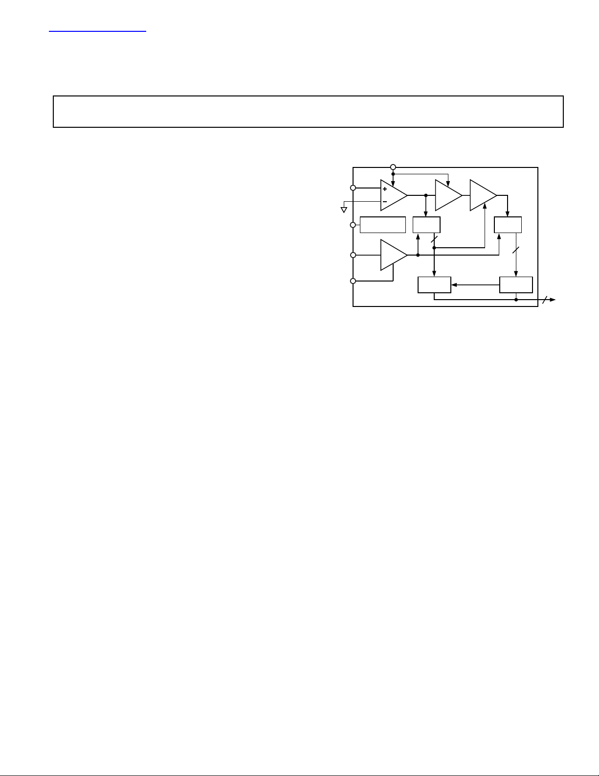
FUNCTIONAL BLOCK DIAGRAM
ENCODE
AMP
A
GND
BP
IN
V
OUT
V
REF
REF
T/H T/H
BANDGAP
REFERENCE
REF
AMP
AD9040A
5-BIT
ADC
DECODE
LOGIC
PRODUCT HIGHLIGHTS
1. CMOS compatible logic for direct interface to ASICs.
2. On-board T/H provides excellent high frequency performance on analog inputs, critical for communications and
medical imaging applications.
3. High input impedance and 2 volt p-p input range reduce
need for external amplifiers.
4. Easy to use; no cumbersome external voltage references
required, allowing denser packing of ADCs for multichannel
applications.
5. Available in 28-lead plastic DIP and SOIC packages.
6. Evaluation board includes AD9040AJR, reconstruction
DAC, and latches. Space is available near the analog input
and digital outputs of the converter for additional circuits.
Order as part number AD9040A/PCB (schematic shown in
data sheet).
ARRAY
ERROR
CORRECTION
6-BIT
ADC
DECODE
LOGIC
10
REV. B
Information furnished by Analog Devices is believed to be accurate and
reliable. However, no responsibility is assumed by Analog Devices for its
use, nor for any infringements of patents or other rights of third parties
which may result from its use. No license is granted by implication or
otherwise under any patent or patent rights of Analog Devices.
One Technology Way, P.O. Box 9106, Norwood, MA 02062-9106, U.S.A.
Tel: 781/329-4700 World Wide Web Site: http://www.analog.com
Fax: 781/326-8703 © Analog Devices, Inc., 1999

AD9040A–SPECIFICATIONS
(+VS = VD = +5 V; –VS = –5 V; internal reference: ENCODE = 40.5 MSPS unless
ELECTRICAL CHARACTERISTICS
Parameter (Conditions) Temp Level Min Typ Max Units
RESOLUTION 10 Bits
DC ACCURACY
Differential Nonlinearity +25°C I 1.0 2.0 LSB
Integral Nonlinearity +25°C I 1.0 2.0 LSB
No Missing Codes Full VI Guaranteed
Gain Error +25°CI ±0.5 ±1.5 % FS
Gain Tempco
ANALOG INPUT
Input Voltage Range +25°C V 2 V p-p
Input Offset Voltage +25°CI ±2 ±25 mV
Input Bias Current +25°CI 7 15 µA
Input Resistance +25°C I 200 350 kΩ
Input Capacitance +25°CV 5 pF
Analog Bandwidth +25°C V 48 MHz
BANDGAP REFERENCE
Output Voltage Full VI 2.4 2.6 V
Temperature Coefficient
SWITCHING PERFORMANCE
Maximum Conversion Rate +25°C I 40 MSPS
Minimum Conversion Rate +25°C IV 2 10 MSPS
Aperture Delay (t
Aperture Uncertainty (Jitter) +25°C V 7 ps, rms
Output Propagation Delay (t
DYNAMIC PERFORMANCE
Transient Response +25°CV 25 ns
Overvoltage Recovery Time +25°CV 40 ns
Signal-to-Noise Ratio
f
= 2.3 MHz +25°C I 51 54 dB
IN
f
= 10.3 MHz +25°C I 50 53 dB
IN
Signal-to-Noise Ratio
(Without Harmonics)
f
IN
f
IN
Signal-to-Noise Ratio
f
= = 2.3 MHz +25°C I 52 56 dB
IN
f
= = 10.3 MHz +25°C I 51 55 dB
IN
Signal-to-Noise Ratio
(Without Harmonics)
f
IN
f
IN
2nd Harmonic Distortion
f
= 2.3 MHz +25°C I 56 67 dBc
IN
f
= 10.3 MHz +25°C I 56 65 dBc
IN
3rd Harmonic Distortion
f
= 2.3 MHz +25°C I 58 73 dBc
IN
f
= 10.3 MHz +25°C I 58 70 dBc
IN
Two-Tone Intermodulation +25°C V 62 dBc
Distortion Rejections
Differential Phase +25°C III 0.15 0.5 Degrees
Differential Gain +25°C III 0.25 1.0 %
1
1
) +25°C V 1.9 ns
A
2
)
PD
3
3
= 2.3 MHz +25°C I 52 55 dB
= 10.3 MHz +25°C I 51 54 dB
3, 4
3, 4
= 2.3 MHz +25°C I 53 57 dB
= 10.3 MHz +25°C I 53 56 dB
otherwise noted)
Test AD9040AJN/JR
Full VI 2.5 LSB
Full VI 2.5 LSB
Full VI ±2% FS
Full V ±70 ppm/°C
Full VI ±30 mV
Full VI 25 µA
Full V ±40 ppm/°C
+25°C I 7.5 10 12 ns
Full IV 6 14 ns
–2–
REV. B

AD9040A
Test AD9040AJN/JR
Parameter (Conditions) Temp Level Min Typ Max Units
ENCODE INPUT
Logic “1” Voltage Full VI 4.0 V
Logic “0” Voltage Full VI 1.0 V
Logic “1” Current Full VI ±1 µA
Logic “0” Current Full VI ±1 µA
Input Capacitance +25°CV 14 pF
Encode Pulsewidth (High) (t
Encode Pulsewidth (Low) (tEL)
DIGITAL OUTPUTS
Logic “1” Voltage Full VI 4.95 V
Logic “0” Voltage Full VI 0.05 V
Output Coding Offset Binary
POWER SUPPLY
V
Supply Current Full VI 13 20 mA
D
+V
Supply Current Full VI 89 110 mA
S
–V
Supply Current Full VI 87 105 mA
S
Power Dissipation Full VI 0.94 1.2 W
Power Supply
Rejection Ratio (PSRR)
NOTES
1
“Gain Tempco” is for converter using internal reference; “Temperature
Coefficient” is for bandgap reference only.
2
Output propagation delay (tPD) is measured from the 50% point of the falling
edge of the encode command to the min/max voltage levels of the digital
outputs with 10 pF maximum loads.
3
RMS signal to rms noise with analog input signal 1 dB below full scale at
specified frequency.
4
ENCODE = 32 MSPS.
5
3rd order intermodulation measured with analog input frequencies of 2.3 MHz
and 2.4 MHz at 7 dB below full scale.
6
For rated performance at 40 MSPS, duty cycle of encode command should be
50% ±10%.
7
Measured as the ratio of the change in offset voltage for a 5% change in +V
or –VS.
Specifications subject to change without notice.
EXPLANATION OF TEST LEVELS
Test Level
I – 100% Production Tested.
II – 100% production tested at +25°C, and sample tested at
specified temperatures. AC testing done on sample basis.
III – Sample Tested Only.
IV – Parameter is guaranteed by design and characterization
testing.
V – Parameter is a typical value only.
VI – All devices are 100% production tested at +25°C. 100%
production tested at temperature extremes for military
temperature devices; guaranteed by design and character-
ization testing for industrial devices.
6
)
EH
6
7
+25°C IV 10 100 ns
+25°C IV 10 100 ns
+25°CI ±15 mV/V
ABSOLUTE MAXIMUM RATINGS
1
±VS . . . . . . . . . . . . . . . . . . . . . . . . . . . . . . . . . . . . . . . . . . ±7 V
V
. . . . . . . . . . . . . . . . . . . . . . . . . . . . . . . . . . . . . . . . . . . +7 V
D
ANALOG IN . . . . . . . . . . . . . . . . . . . . . . . . . . . . –V
to +V
S
DIGITAL INPUTS . . . . . . . . . . . . . . . . . . . . . . . . . 0 V to +V
V
Input . . . . . . . . . . . . . . . . . . . . . . . . . . . . . . . . 0 V to +V
REF
Digital Output Current . . . . . . . . . . . . . . . . . . . . . . . . . 20 mA
Operating Temperature
AD9040AJN/JR . . . . . . . . . . . . . . . . . . . . . . . .0°C to +70°C
S
Maximum Junction Temperature
Storage Temperature . . . . . . . . . . . . . . . . . –65°C to +150°C
2
(JN/JR Suffixes) . . . +150°C
Lead Soldering Temp (10 sec) . . . . . . . . . . . . . . . . . . . +300°C
NOTES
1
Absolute maximum ratings are limiting values to be applied individually, and
beyond which the serviceability of the circuit may be impaired. Functional
operability is not necessarily implied. Exposure to absolute maximum rating
conditions for an extended period of time may affect device reliability.
2
Typical thermal impedances (parts soldered to board):
N Package (Plastic DIP): θJA = 42°C/W; θJC = 10°C/W.
R Package (SOIC): θJA = 47°C/W; θJC = 10°C/W.
S
S
S
REV. B
ORDERING GUIDE
Model Temperature Range Package Description Package Option
AD9040AJN 0°C to +70°C 28-Lead Plastic DIP N-28
AD9040AJR 0°C to +70°C 28-Lead SOIC Package R-28
AD9040A/PWB Printed Circuit Board (Only) of Evaluation Circuit
AD9040A/PCB Complete Evaluation Board, Assembled and Tested,
Including AD9040AJR
–3–

AD9040A
A
ENCODE
DIGITAL
OUTPUTS
N
IN
N + 1
t
A
tEHt
EL
t
PD
N – 3 N – 2 N – 1
#2 #3
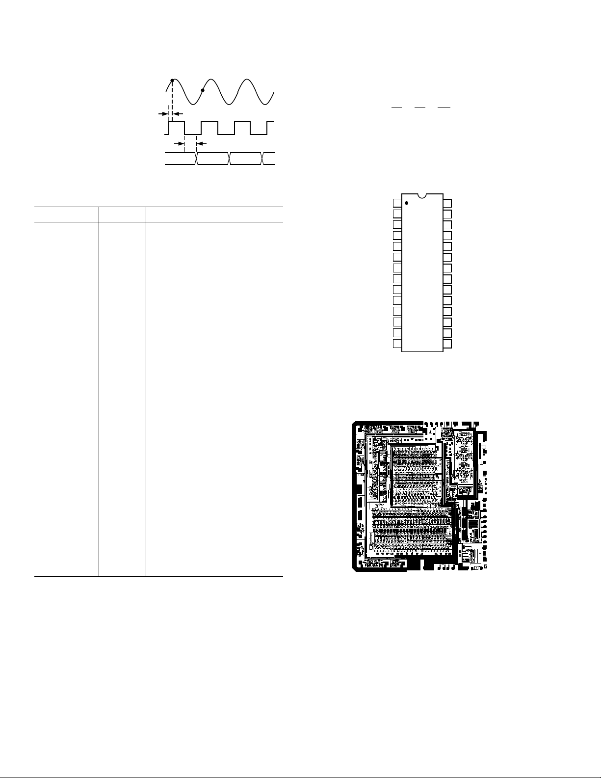
Figure 1. Timing Diagram
t
APERTURE DELAY
A
t
PULSEWIDTH HIGH
EH
t
PULSEWIDTH LOW
EL
OUTPUT PROP DELAY
t
PD
MIN TYP MAX
1.9
10
10 100
7.5
10ns
100
12
PIN FUNCTION DESCRIPTIONS
Pin No. Name Function
1, 12, 21 –V
S
5 V Power Supply
2, 4, 11, 14, 22 GND Ground
3, 10 +V
5V
S
OUT
Analog +5 V Power Supply
Internal Bandgap Voltage
Reference (Nominally +2.5 V)
6V
REF
Noninverting Input to Reference
Amplifier. Voltage reference for
ADC is connected here.
7BP
REF
External Connection for (0.1 µF)
Reference Bypass Capacitor
8 NC No Connection Internally
9 ENCODE Encode Clock Input to ADC.
Internal T/H placed in hold mode
(ADC is encoding) on rising edge.
13 A
IN
Noninverting Input to T/H
Amplifier
15 OR Out-of-Range Condition Output.
Active high when analog input
exceeds input range of ADC by
1 LSB (<FS –1 LSB or >+FS
+ 1 LSB).
16 D9 (MSB) Most Significant Bit of ADC
Output; TTL/CMOS Compatible
17–20 D8–D5 Digital Output Bits of ADC; TTL/
CMOS Compatible
23 V
D
Digital +5 V Power Supply
24–27 D4–D1 Digital Output Bits of ADC;
TTL/CMOSL Compatible
28 D0 (LSB) Least Significant Bit of ADC
Output; TTL/CMOS Compatible
–V
GND
+V
GND
V
OUT
V
REF
BP
REF
NC
ENCODE
+V
GND
–V
A
GND
1
S
2
3
S
4
5
6
AD9040A
7
TOP VIEW
(Not to Scale)
8
9
10
S
11
12
S
13
IN
14
NC = NO CONNECT
28
27
26
25
24
23
22
21
20
19
18
17
16
15
D0 (LSB)
D1
D2
D3
D4
V
D
GND
–V
S
D5
D6
D7
D8
D9 (MSB)
OR
PDIP and SOIC Pinouts
S
IN
GND
GND
–V
A
+V
S
ENCODE
NC
BP
REF
V
REF
V
OUT
GND
S
+V
D6
–V
DGND
D8
D7
D5
S
V
D
D4
D3
D2
D1
OR
D9 (MSB)
S
–V
D0 (LSB)
GND
DIE LAYOUT AND MECHANICAL INFORMATION
Die Dimensions . . . . . . . . . . . . . . . . . 204 × 185 × 21 (±1) mils
Pad Dimensions . . . . . . . . . . . . . . . . . . . . . . . . . . . . . 4 × 4 mils
Metalization . . . . . . . . . . . . . . . . . . . . . . . . . . . . . . . Aluminum
Backing . . . . . . . . . . . . . . . . . . . . . . . . . . . . . . . . . . . . . . None
Substrate Potential . . . . . . . . . . . . . . . . . . . . . . . . . . . . . . .–V
Transistor Count . . . . . . . . . . . . . . . . . . . . . . . . . . . . . . . 5,070
Passivation . . . . . . . . . . . . . . . . . . . . . . . . . . . . . . . . Oxynitride
Die Attach (JN/JR) . . . . . . . . . . . . . . . . . . . . . . . . . . . . Epoxy
Bond Wire (JN/JR) . . . . . . . . . . . . . . . . . . . . . . . . . . . . . Gold
S
–4–
REV. B
 Loading...