High Speed
a
FEATURES
77 MSPS Encode Rate
Bipolar Input Range
Low Error Rate
Overflow Bit
MIL-STD-883 Compliant Versions Available
APPLICATIONS
QAM Telecommunications
Electronic Warfare (ECM, ECCM, ESM)
Radar Guidance Digitizers
GENERAL DESCRIPTION
The AD9000 is a 6-bit, high speed, analog-to-digital converter
with ECL compatible outputs and a bipolar input stage. The
AD9000 is fabricated in a high performance bipolar process that
allows encode rates up to 77 MSPS.
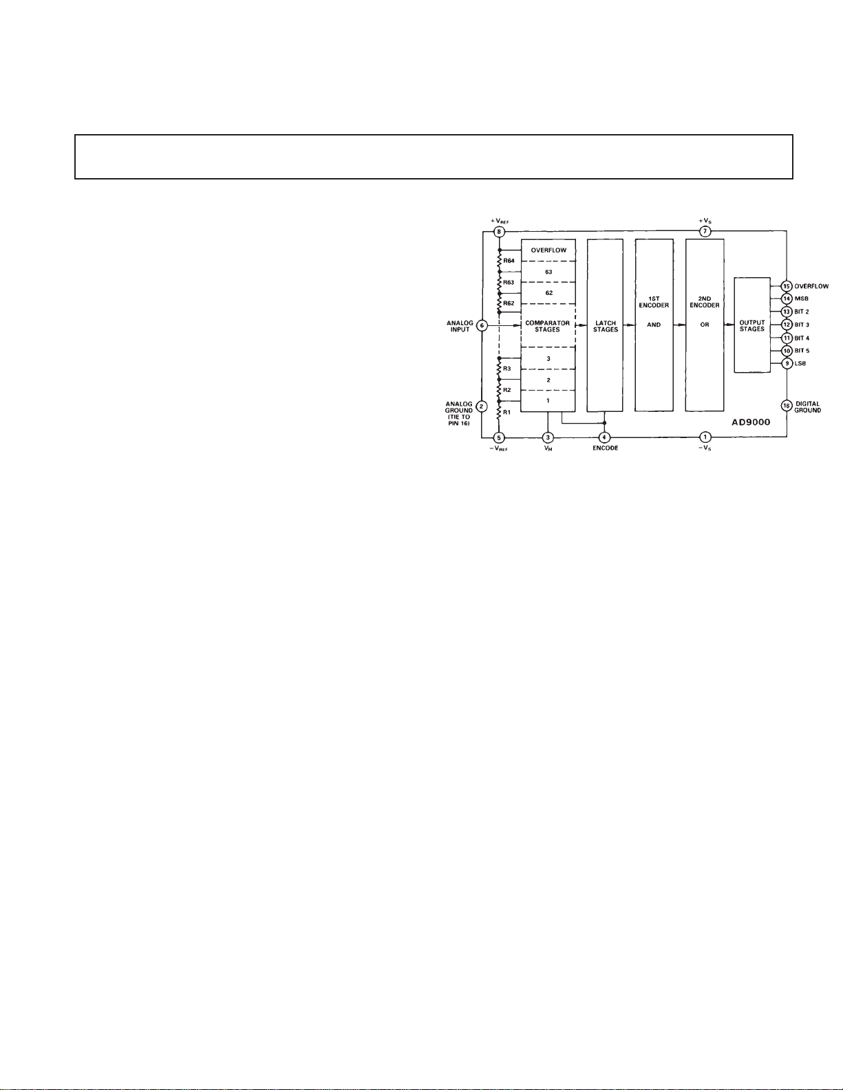
The AD9000 employs the standard flash converter architecture
based on 64 individual comparators which simultaneously
determine the precise analog signal level. The comparators are
followed by two stages of decoding logic, allowing the AD9000
to operate with a very low error rate. The low 35 pF input
capacitance of the AD9000 greatly simplifies the analog driver
stage. An overflow output bit is also incorporated into the
AD9000 design as is a hysteresis control pin to modify comparator sensitivity.
6-Bit A/D Converter
AD9000
FUNCTIONAL BLOCK DIAGRAM
The AD9000 is offered as both a commercial temperature range
device, 0°C to +70°C, and as an extended temperature range
device, –55°C to +125°C. Both versions are available packaged
in a 16-pin ceramic DIP. The extended temperature range
device is also available in a 28-pin ceramic LCC package. The
extended temperature range versions are offered as fully compliant MIL-STD-883 Class B devices.
REV. A
Information furnished by Analog Devices is believed to be accurate and
reliable. However, no responsibility is assumed by Analog Devices for its
use, nor for any infringements of patents or other rights of third parties
which may result from its use. No license is granted by implication or
otherwise under any patent or patent rights of Analog Devices.
One Technology Way, P.O. Box 9106, Norwood, MA 02062-9106, U.S.A.
Tel: 617/329-4700 World Wide Web Site: http://www.analog.com
Fax: 617/326-8703 © Analog Devices, Inc., 1997

AD9000–SPECIFICATIONS
(Supply Voltages = –5.2 V and +5.0 V; Differential Reference Voltage = 2.0 V
ELECTRICAL CHARACTERISTICS
Parameter Temp Min Typ Max Min Typ Max Units
RESOLUTION 6 6 Bits
DC ACCURACY
Differential Linearity +25°C 0.25 0.5 0.25 0.5 LSB
Integral Linearity +25°C 0.25 0.5 0.25 0.5 LSB
No Missing Codes Full GUARANTEED GUARANTEED
INITIAL OFFSET ERROR
Top of Reference Ladder +25°C 0.3 7/8 0.3 7/8 LSB
Bottom of Reference Ladder +25°C 0.25 7/8 0.25 7/8 LSB
Offset Drift Coefficient Full 145 145 µV/°C
ANALOG INPUT
Input Voltage Range Full ±2.0 V ±2.0 V V
Input Bias Current (Sampling)
Input Bias Current (Latched)
Input Resistance +25°C 3.0 3.0 kΩ
Input Capacitance +25°C3550 3550pF
Full Power Bandwidth
REFERENCE INPUT
2
3, 4
Reference Ladder Resistance +25°C 80 200 80 200 Ω
Ladder Temperature Coefficient 0.275 0.275 Ω/°C
Reference Input Bandwidth +25°C 20 20 MHz
DYNAMIC PERFORMANCE
Conversion Rate +25°C5070 7577 MHz
Conversion Time (+ 1 Clock) +25°C 20 13.3 ns
Aperture Delay (t
) +25°C2 2 ns
D
Aperture Uncertainty (Jitter) +25°C25 25 ps
Output Propagation Delay (t
Output Hold Time (t
Transient Response
Overvoltage Recovery Time
Output Rise Time
Output Fall Time
OH
8
10
10
Output Time Skew +25°C 0.4 0.4 ns
1
1
5
6
)
PD
7
)
9
unless otherwise noted)
Commercial Military
08C to +708C –558C to +1258C
AD9000JD AD9000SD/SE
Full 1.0 1.0 LSB
Full 1.0 1.0 LSB
Full 1.5 1.5 LSB
Full 1.5 1.5 LSB
Full 800 800 µA
Full 20 20 µA
+25°C 20 20 MHz
+25°C8 12 8 12 ns
+25°C8 14 8 14 ns
+25°C13 13 ns
+25°C11 11 ns
+25°C 5.0 4.5 ns
+25°C 5.0 4.5 ns
ENCODE INPUT
Logic “l” Voltage Full –1.1 –1.1 V
Logic “0” Voltage Full –1.5 –1.5 V
Logic “1” Current Full 100 100 µA
Logic “0” Current Full 100 100 µA
Input Capacitance +25°C 2.5 5.0 2.5 5.0 pF
ENCODE Pulse Width High (t
ENCODE Pulse Width Low (t
) +25°C 6.6 6.6 ns
PWH
) +25°C 6.6 6.6 ns
PWL
–2–
REV. A

AD9000
ELECTRICAL CHARACTERISTICS
(Continued)
Commercial Military
08C to +708C –558C to +1258C
AD9000JD AD9000SD/SE
Parameter Temp Min Typ Max Min Typ Max Units
AC LINEARITY
Dynamic Linearity
11
12
+25°C 0.5 0.5 LSB
In-Band Harmonics
(DC to l MHz) +25°C 44 44 dBc
(l MHz to 5 MHz) +25°C 42 42 dBc
(5 MHz to 8 MHz) +25°C 38 38 dBc
Signal-to-Noise Ratio
Signal-to-Noise Ratio
Two Tone Intermodulation Rejection
Noise Power Ratio (NPR)
DIGITAL OUTPUTS
13
14
16
5
+25°C3133 3133 dB
+25°C4042 4042 dB
15
+25°C 46 46 dBc
+25°C 30 30 dBc
Logic “l” Voltage Full –1.1 –1.1 V
Logic “0” Voltage Full –1 .5 –1.5 V
POWER SUPPLY
17
Positive Supply Current (+5.0 V) +25°C6070 6070mA
Full 75 75 mA
Negative Supply Current (–5.2 V) +25°C6880 6880mA
Full 85 85 mA
Nominal Power Dissipation +25°C 675 675 mW
Reference Ladder Dissipation +25°C20 20 mW
NOTES
1
AIN = +V
2
Determined by 3 dB reduction in reconstructed output at 75 MSPS.
3
Under normal operating conditions, the analog input voltages should not
exceed nominal ±2 V operating range, nor the supply voltages (+VS and –VS),
whichever is smaller.
4
Under normal operating conditions the differential reference voltage may
range from ±0.5 V to ±2 V; +V
5
Output terminated with 100 Ω resistors to –2.0 V.
6
Measured from the leading edge of ENCODE to data out on Bit 1 (MSB).
7
Measured from the trailing edge of ENCODE to data out on Bit 1 (MSB).
8
For full-scale step input, 6-bit accuracy is attained in specified time.
ABSOLUTE MAXIMUM RATINGS
REF
.
≥ –V
REF
.
1
REF
Positive Supply Voltage . . . . . . . . . . . . . . . . . . . 0.3 V to +6 V
Negative Supply Voltage . . . . . . . . . . . . . . . . . 6.0 V to +0.3 V
Analog-to-Digital Ground Voltage Differential . . . . . . . . . 0.5
Analog Input Voltages (A
Differential Reference Voltage (+V
ENCODE Input Voltage . . . . . . . . . . . . . . . . . . . . – V
IN
, +V
REF
, –V
)2 . . . . . . . . . . +3 V
REF
REF
to –V
)3 . . . . . . . 6 V
REF
to 0 V
S
HYSTERESIS Control Voltage . . . . . . . . . . . . 0 V to + 3.0 V
Digital Output Current . . . . . . . . . . . . . . . . . . . . . . . . 20 mA
Power Dissipation (+25°C Free Air)
4
. . . . . . . . . . . . 745 mW
Operating Temperature Range
AD9000JD . . . . . . . . . . . . . . . . . . . . . . . . . . . . 0°C to +70°C
9
Recovers to 6-bit accuracy in specified time, after 150% full-scale input
overvoltage.
10
Measured on Bit 1 (MSB) only.
11
Measured at 50 MSPS encode rate.
12
Analog input frequency = 15 MHz.
13
RMS signal to RMS noise, with 540 kHz analog input signal.
14
Peak-to-peak signal to rms noise, with 540 kHz analog input signal.
15
f1 = 9.3 MHz, f2 = 7.6 MHz; Encode = 42 MHz.
16
DC to 8.2 MHz noise bandwidth with 3.886 MHz slot.
17
Supply voltage should remain stable within ±5% for normal operation.
Specifications subject to change without notice.
NOTES
1
Absolute maximum ratings are limiting values, to be applied individually, and
beyond which serviceability of the circuit may be impaired. Functional operability under any of these conditions is not necessarily implied. Exposure to
absolute maximum rating conditions for extended periods may affect device
reliability.
2
Under normal operating conditions, the analog input voltages should not
exceed nominal +2 V operating range, nor the supply voltages (+VS and –VS),
whichever is smaller.
3
Under normal operating conditions the differential reference voltage may range
from ±0.5 V to ±2 V; +V
4
Typical thermal impedances . . .
16-Pin Ceramic θJA = 67°C/W; θJC = 7°C/W
28-Pin LCC θJA = 62°C/W; θJC = 14°C/W
REF
≥ –V
REF.
AD9000SD/SE . . . . . . . . . . . . . . . . . . . . . . –55°C to +125°C
Storage Temperature Range . . . . . . . . . . . . –65°C to +150°C
Junction Temperature . . . . . . . . . . . . . . . . . . . . . . . . +175°C
Lead Soldering Temperature (10 sec) . . . . . . . . . . . . +300°C
REV. A
–3–
 Loading...