8-Bit Octal, 4-Quadrant
V
IN
RR
V
OUT
V
OUT
= VIN • (D/128 – 1)
a
FEATURES
Low Cost
Replaces 8 Potentiometers
50 kHz 4-Quadrant Multiplying Bandwidth
Low Zero Output Error
Eight Individual Channels
3-Wire Serial Input
500 kHz Update Data Loading Rate
±3 V Output Swing
Midscale Preset, Zero Volts Out
APPLICATIONS
Automatic Adjustment
Trimmer Replacement
Vertical Deflection Amplitude Adjustment
Waveform Generation and Modulation
GENERAL DESCRIPTION
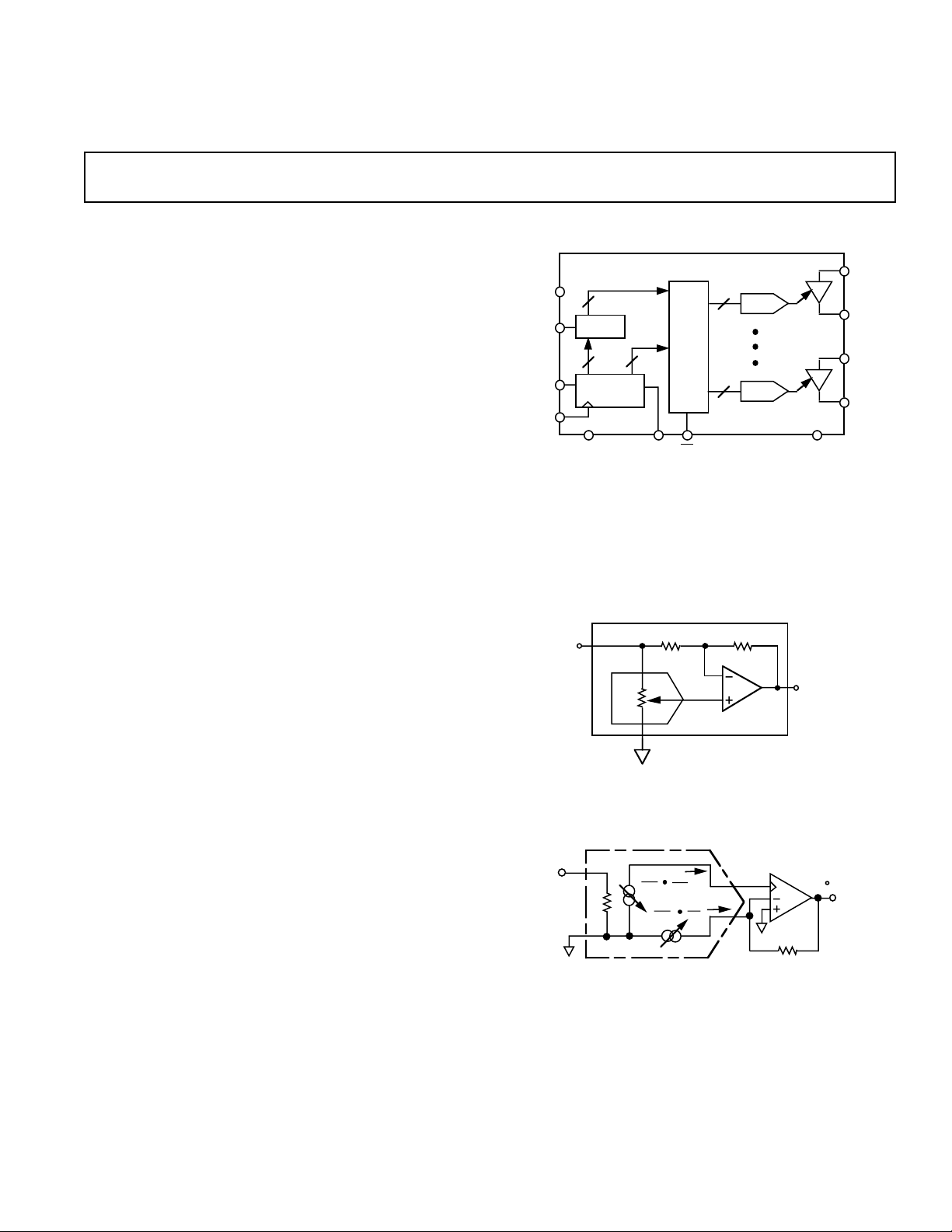
The AD8842 provides eight general purpose digitally controlled
voltage adjustment devices. The TrimDAC® capability allows
replacement of the mechanical trimmer function in new designs.
The AD8842 is ideal for ac or dc gain control of up to 50 kHz
bandwidth signals. The four-quadrant multiplying capability is
useful for signal inversion and modulation often found in video
vertical deflection circuitry.
Internally the AD8842 contains eight voltage output digital-toanalog converters, each with separate voltage inputs. A new
current conveyor amplifier design performs the four-quadrant
multiplying function with a single amplifier at the output of the
current steering digital-to-analog converter. This approach offers an improved constant input resistance performance versus
previous voltage switched DACs used in TrimDAC circuits,
eliminating the need for additional input buffer amplifiers.
Each DAC has its own DAC register that holds its output state.
These DAC registers are updated from an internal serial-toparallel shift register that is loaded from a standard 3-wire serial
input digital interface. Twelve data bits make up the data word
clocked into the serial input register. This data word is decoded
where the first 4 bits determine the address of the DAC register
to be loaded with the last 8 bits of data. A serial data output pin
at the opposite end of the serial register allows simple daisy
chaining in multiple DAC applications without additional external decoding logic.
Multiplying, CMOS TrimDAC
AD8842
FUNCTIONAL BLOCK DIAGRAM
DECODED
V
LD
SDI
CLK
DD
ADDRESS
8
LOGIC
4
SERIAL
REGISTER
GND
8
DATA
8 X 8
DAC
R
E
G
I
S
T
E
R
S
PRSDO
8
DAC A
AD8842
8
DAC H
The AD8842 consumes only 95 mW from ±5 V power supplies.
For single 5 V supply applications consult the DAC-8841. The
AD8842 is pin compatible with the 1 MHz multiplying bandwidth DAC8840. The AD8842 is available in 24-pin plastic
DIP and surface mount SOL-24 packages.
Figure 1. Functional Circuit of One 4-Quadrant
Multiplying Channel
CURRENT CONVEYOR
I1
I2
AMPLIFIER
= VIN (D/128–1)
R
V
IN
REF
R
256
D
(1- D)
256
V
IN
R
V
IN
R
VINA
G
V
A
OUT
VINH
G
V
H
OUT
V
SS
V
OUT
TrimDAC is a registered trademark of Analog Devices, Inc.
The current conveyor amplifier is a patented circuit belonging to Analog
Devices, Inc.
REV. 0
Information furnished by Analog Devices is believed to be accurate and
reliable. However, no responsibility is assumed by Analog Devices for its
use, nor for any infringements of patents or other rights of third parties
which may result from its use. No license is granted by implication or
otherwise under any patent or patent rights of Analog Devices.
Figure 2. Actual Current Conveyor Implementation of
Multiplying DAC Channel
One Technology Way, P.O. Box 9106, Norwood. MA 02062-9106, U.S.A.
Tel: 617/329-4700 Fax: 617/326-8703

AD8842–SPECIFICATIONS
ELECTRICAL CHARACTERISTICS
(VDD = +5 V, V
= –5 V, All VINx = +3 V, TA = –40°C to +85°C, unless otherwise noted.)
SS
Parameter Symbol Conditions Min Typ Max Units
STATIC ACCURACY—All Specifications Apply for DACs A, B, C, D, E, F, G, H
Resolution N 8 Bits
Integral Nonlinearity Error INL ±0.2 ±1 LSB
Differential Nonlinearity DNL All Devices Monotonic ±0.4 ±1 LSB
Full-Scale Gain Error G
Output Offset V
Output Offset Drift TCV
VOLTAGE INPUTS—Applies to All Inputs V
Input Voltage Range
1
Input Resistance R
Input Capacitance C
DAC OUTPUTS—Applies to All Outputs V
Voltage Range
1
Output Current I
Capacitive Load C
DYNAMIC PERFORMANCE—Applies to All DACs
Full Power Gain Bandwidth
1
FSE
BZE
PR = 0, Sets D = 80
PR = 0, Sets D = 80
BZ
x
IN
IVR ±3 ±4V
IN
IN
x
OUT
OVR RL = 10 kΩ±3±4V
OUT
L
∆V
No Oscillation 500 pF
GBW VINx = ± 3 VP, RL = 2 kΩ, CL = 10 pF 10 50 kHz
H
H
12 19 kΩ
< 1.5 LSB ±3mA
OUT
2 LSB
525mV
5 µV/°C
9pF
Slew Rate Measured 10% to 90%
Positive SR+ ∆V
Negative SR– ∆V
Total Harmonic Distortion THD V
Spot Noise Voltage e
Output Settling Time t
Channel-to-Channel Crosstalk C
N
S
T
x = +5.5 V 0.5 1.0 V/µs
OUT
x = –5.5 V 1.0 1.8 V/µs
OUT
x = 4 V p-p, D = FFH, f = 1 kHz, 0.01 %
IN
= 80 kHz, RL = 1 kΩ
f
LPF
f = 1kHz, VIN = 0 V 78 nV/√Hz
±1 LSB Error Band, D = 00H to FF
D = FF
H
to 00
H
H
2.9 µs
5.4 µs
Measured Between Adjacent
Channels, f = 100 kHz 72 dB
Digital Feedthrough Q VINx = 0 V, D = 0 to 255
10
5 nV-s
POWER SUPPLIES
Positive Supply Current I
Negative Supply Current I
Power Dissipation
2
P
DD
SS
DISS
Power Supply Rejection PSRR
PR = 0 V 10 14 mA
PR = 0 V 9 13 mA
95 135 mW
PR = 0 V, ∆VDD = ±5% 0.0001 0.01 %/%
Power Supply Range PSR VDD, |VSS| 4.75 5.00 5.25 V
DIGITAL INPUTS
Logic High V
Logic Low V
Input Current I
Input Capacitance C
IH
IL
L
IL
2.4 V
7pF
Input Coding Offset Binary
DIGITAL OUTPUT
Logic High V
Logic Low V
TIMING SPECIFICATIONS
1
Input Clock Pulse Width tCH, t
Data Setup Time t
Data Hold Time t
CLK to SDO Propagation Delay t
DAC Register Load Pulse Width t
Preset Pulse Width t
Clock Edge to Load Time t
Load Edge to Next Clock Edge t
NOTES
1
Guaranteed by design, not subject to production test.
2
Calculated limit = 5 V × (IDD + ISS).
Specifications subject to change without notice.
DS
DH
PD
LD
PR
CKLD
LDCK
OH
OL
IOH = –0.4 mA 3.5 V
IOL = 1.6 mA 0.4 V
CL
60 ns
40 ns
20 ns
70 ns
50 ns
30 ns
60 ns
0.8 V
±10 µA
80 ns
REV. 0–2–

1
SDI
0
1
CLK
0
1
LD
0
+3V
V
OUT
0V
DETAIL SERIAL DATA INPUT TIMING (PR = “1”)
1
SDI
(DATA IN)
(DATA OUT)
0
1
SDO
0
1
CLK
0
1
LD
0
+3V
V
OUT
0V
PRESET TIMING
1
PR
0
+3V
V
OUT
0V
A3 A2 A1 A0 D7 D6 D5 D4 D3 D2 D1 D0
t
CH
t
PR
t
S
±1 LSB ERROR BAND
t
CL
Ax or Dx
t
DS
t
DH
t
PD
t
CKLD
±1 LSB
t
LD
t
S
±1 LSB ERROR BAND
t
AD8842
DAC REGISTER LOAD
LDCK
±1 LSB
Figure 3. Timing Diagram
ABSOLUTE MAXIMUM RATINGS
(TA = +25°C unless otherwise noted)
VDD to GND . . . . . . . . . . . . . . . . . . . . . . . . . . . . –0.3 V, +7 V
V
to GND . . . . . . . . . . . . . . . . . . . . . . . . . . . . . +0.3 V, –7 V
SS
x to GND . . . . . . . . . . . . . . . . . . . . . . . . . . . . . . . VDD, V
V
IN
V
x to GND . . . . . . . . . . . . . . . . . . . . . . . . . . . . . VDD, V
OUT
Short Circuit I
x to GND . . . . . . . . . . . . . . . . . Continuous
OUT
Digital Input & Output Voltage to GND . . . . . . . . . . V
DD
SS
SS
, 0 V
Model Range* Description Option
AD8842AN XIND 24-Pin 300mil P-DIP N-24
AD8842AR XIND 24-Pin 300mil SOIC SOL-24
*XIND = –40°C to +85°C. The AD8842 contains 2452 transistors.
ORDERING GUIDE
Temperature Package Package
Operating Temperature Range . . . . . . . . . . . . –40°C to +85°C
Maximum Junction Temperature (T
Max) . . . . . . . . . +150°C
J
Storage Temperature . . . . . . . . . . . . . . . . . . . –65°C to +150°C
Lead Temperature (Soldering, 10 sec) . . . . . . . . . . . . +300°C
Package Power Dissipation . . . . . . . . . . . . . . .(T
Thermal Resistance θ
JA,
Max–T
J
)/θ
A
JA
SOIC (SOL-24) . . . . . . . . . . . . . . . . . . . . . . . . . . . . 70°C/W
P-DIP (N-24) . . . . . . . . . . . . . . . . . . . . . . . . . . . . . 57°C/W
CAUTION
ESD (electrostatic discharge) sensitive device. Electrostatic charges as high as 4000 V readily
accumulate on the human body and test equipment and can discharge without detection.
Although the AD8842 features proprietary ESD protection circuitry, permanent damage may
occur on devices subjected to high energy electrostatic discharges. Therefore, proper ESD
precautions are recommended to avoid performance degradation or loss of functionality.
WARNING!
ESD SENSITIVE DEVICE
REV. 0 –3–

AD8842
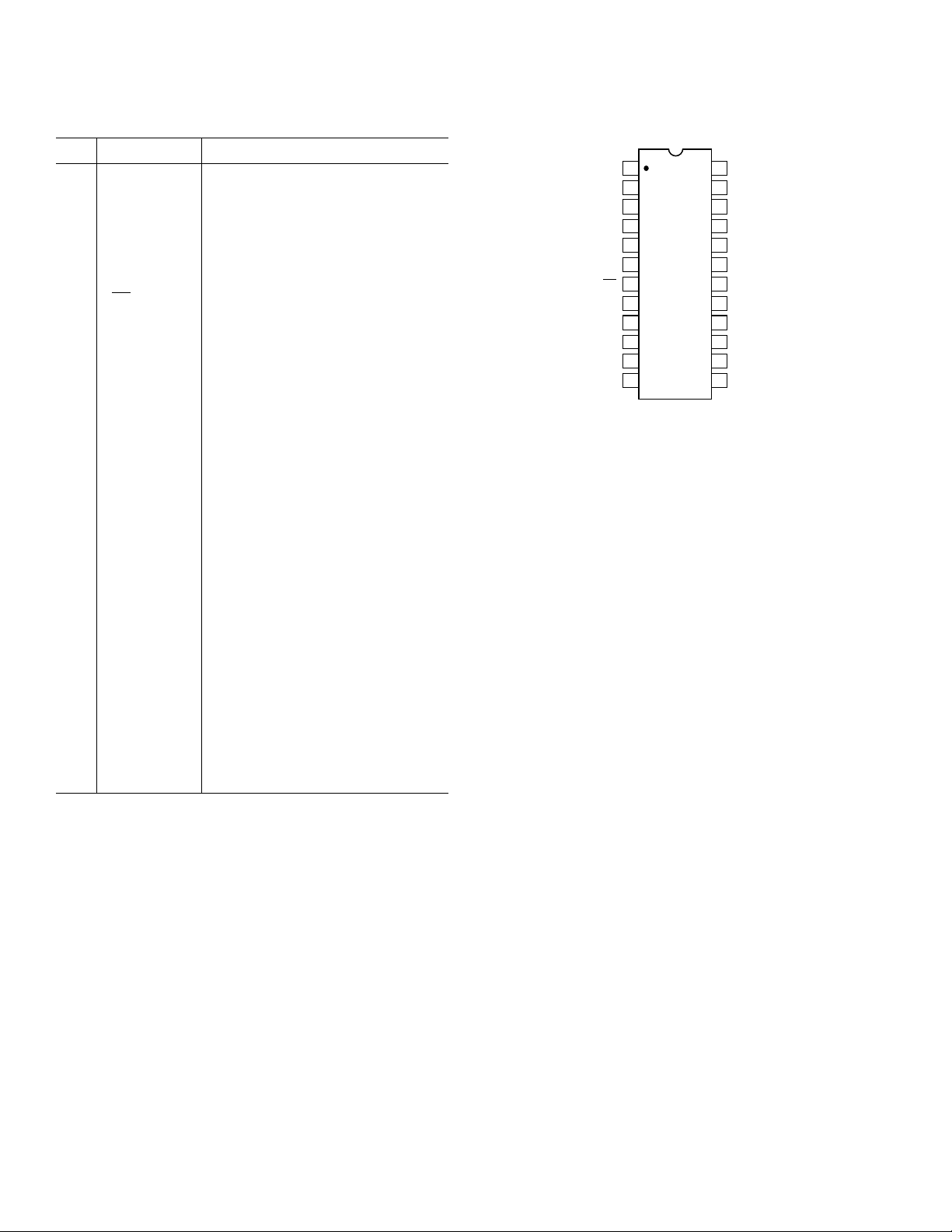
PIN DESCRIPTION
Pin Mnemonic Description
1V
2V
3V
4V
5V
C DAC C Output
OUT
B DAC B Output
OUT
A DAC A Output
OUT
B DAC B Reference Input
IN
A DAC A Reference Input
IN
6 GND Ground
7
8V
9V
10 V
11 V
12 V
13 V
14 V
15 V
PR Preset Input, active low, all DAC
registers = 80
E DAC E Reference Input
IN
F DAC F Reference Input
IN
E DAC E Output
OUT
F DAC F Output
OUT
G DAC G Output
OUT
H DAC H Output
OUT
G DAC G Reference Input
IN
H DAC H Reference Input
IN
H
16 LD Load DAC Register Strobe, active-
high input that transfers the data
bits from the serial-input register
into the decoded DAC register.
SDI and CLK inputs are disabled
when LD is high. See Tables I and II
17 CLK Serial Clock Input, positive edge
triggered
18 SDO Serial Data Output, active totem
pole output
19 V
SS
Negative 5 V Power Supply
20 SDI Serial Data Input
21 V
22 V
23 V
24 V
DD
D DAC D Reference Input
IN
C DAC C Reference Input
IN
D DAC D Output
OUT
Positive 5 V Power Supply
PIN CONFIGURATION
V
C
1
OUT
V
B
2
OUT
V
A
3
OUT
VINB
4
5
VINA
GND
PR
VINE CLK
VINF LD
V
OUT
V
OUT
V
OUT
AD8842
6
TOP VIEW
7
(Not to Scale)
817
916
E VINH
10 15
F VING
11
11
G VINH
12 13
24
23
22
21
20
19
18
14
V
OUT
VINC
VIND
V
DD
SDI
V
SS
SDO
D
REV. 0–4–
 Loading...