Analog Devices AD7846KP, AD7846KN, AD7846JN, AD7846AQ, AD7846AP Datasheet
...
LC2MOS
a
FEATURES
16-Bit Monotonicity over Temperature
ⴞ2 LSBs Integral Linearity Error
Microprocessor Compatible with Readback Capability
Unipolar or Bipolar Output
Multiplying Capability
Low Power (100 mW Typical)
GENERAL DESCRIPTION
The AD7846 is a 16-bit DAC constructed with Analog Devices’
2
MOS process. It has V
LC
an on-chip output amplifier. These can be configured to give a
unipolar output range (0 V to +5 V, 0 V to +10 V) or bipolar
output ranges (±5 V, ±10 V).
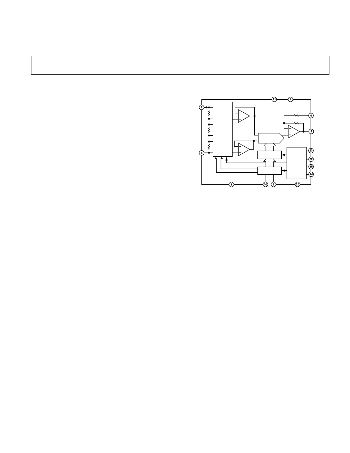
The DAC uses a segmented architecture. The 4 MSBs in the
DAC latch select one of the segments in a 16-resistor string.
Both taps of the segment are buffered by amplifiers and fed to a
12-bit DAC, which provides a further 12 bits of resolution. This
architecture ensures 16-bit monotonicity. Excellent integral
linearity results from tight matching between the input offset
voltages of the two buffer amplifiers.
In addition to the excellent accuracy specifications, the AD7846
also offers a comprehensive microprocessor interface. There are
16 data I/O pins, plus control lines (CS, R/W, LDAC and CLR).
R/W and CS allow writing to and reading from the I/O latch.
This is the readback function which is useful in ATE applications. LDAC allows simultaneous updating of DACs in a multiDAC system and the CLR line will reset the contents of the
DAC latch to 00 . . . 000 or 10 . . . 000 depending on the state
of R/W. This means that the DAC output can be reset to 0 V in
both the unipolar and bipolar configurations.
The AD7846 is available in 28-lead plastic, ceramic, and PLCC
packages.
REF+
and V
reference inputs and
REF–
16-Bit Voltage Output DAC
AD7846
FUNCTIONAL BLOCK DIAGRAM
V
V
V
V
REF +
REF –
R
R
R
16
SEGMENT
SWITCH
MATRIX
4
A2
A1
V
SS
AD7846
12-BIT DAC
12
DAC LATCH
12
I/O LATCH
DB15 DB0
PRODUCT HIGHLIGHTS
1. 16-Bit Monotonicity
The guaranteed 16-bit monotonicity over temperature makes
the AD7846 ideal for closed-loop applications.
2. Readback
The ability to read back the DAC register contents minimizes
software routines when the AD7846 is used in ATE systems.
3. Power Dissipation
Power dissipation of 100 mW makes the AD7846 the lowest
power, high accuracy DAC on the market.
DD
CC
R
R
A3
CONTROL
LOGIC
DGND
R
IN
V
OUT
CS
R/ W
LDAC
CLR
REV. E
Information furnished by Analog Devices is believed to be accurate and
reliable. However, no responsibility is assumed by Analog Devices for its
use, nor for any infringements of patents or other rights of third parties
which may result from its use. No license is granted by implication or
otherwise under any patent or patent rights of Analog Devices.
One Technology Way, P.O. Box 9106, Norwood, MA 02062-9106, U.S.A.
Tel: 781/329-4700 World Wide Web Site: http://www.analog.com
Fax: 781/326-8703 © Analog Devices, Inc., 2000

(V
= +14.25 V to +15.75 V; VSS = –14.25 V to –15.75 V; VCC = +4.75 V to +5.25 V.
DD
V
AD7846–SPECIFICATIONS
loaded with 2 k⍀, 1000 pF to 0 V; V
OUT
1
specifications T
MIN
to T
MAX
, unless otherwise noted.)
= +5 V; RIN connected to 0 V. All
REF+
Parameter J, A Versions K, B Versions Unit Test Conditions/Comments
RESOLUTION 16 16 Bits
UNIPOLAR OUTPUT V
Relative Accuracy @ +25°C ±12 ±4 LSB typ 1 LSB = 153 µV
T
to T
MIN
Differential Nonlinearity Error ±1 ±0.5 LSB max All Grades Guaranteed Monotonic
MAX
±16 ±8 LSB max
Gain Error @ +25°C ±12 ±6 LSB typ V
T
to T
MIN
MIN
to T
2
2
MAX
MAX
Offset Error @ +25°C ±12 ±6 LSB typ
T
Gain TC
Offset TC
±16 ±16 LSB max
±16 ±16 LSB max
±1 ±1 ppm FSR/°C typ
±1 ±1 ppm FSR/°C typ
BIPOLAR OUTPUT V
Relative Accuracy @ +25°C ±6 ±2 LSB typ 1 LSB = 305 µV
T
to T
MIN
Differential Nonlinearity Error ±1 ±0.5 LSB max All Grades Guaranteed Monotonic
MAX
±8 ±4 LSB max
Gain Error @ +25°C ±6 ±4 LSB typ V
to T
T
MIN
MAX
±16 ±16 LSB max
Offset Error @ +25°C ±6 ±4 LSB typ V
T
MIN
to T
MAX
±16 ±12 LSB max
= 0 V, V
REF–
Load = 10 MΩ
OUT
= –5 V, V
REF–
Load = 10 MΩ
OUT
Load = 10 MΩ
OUT
= 0 V to +10 V
OUT
= –10 V to +10 V
OUT
Bipolar Zero Error @ +25°C ±6 ±4 LSB typ
T
to T
MIN
MAX
Gain TC
Offset TC
2
2
Bipolar Zero TC
2
±12 ±8 LSB max
±1 ±1 ppm FSR/°Ctyp
±1 ±1 ppm FSR/°Ctyp
±1 ±1 ppm FSR/°Ctyp
REFERENCE INPUT
Input Resistance 20 20 kΩ min Resistance from V
40 40 kΩ max Typically 30 kΩ
V
Range VSS + 6 to VSS + 6 to Volts
REF+
V
Range VSS + 6 to VSS + 6 to Volts
REF–
VDD – 6 VDD – 6
VDD – 6 VDD – 6
REF+
to V
REF –
OUTPUT CHARACTERISTICS
Output Voltage Swing VSS + 4 to VSS + 4 to V max
VDD – 3 VDD – 3
Resistive Load 2 2 kΩ min To 0 V
Capacitive Load 1000 1000 pF max To 0 V
Output Resistance 0.3 0.3 Ω typ
Short Circuit Current ±25 ±25 mA typ To 0 V or Any Power Supply
DIGITAL INPUTS
VIH (Input High Voltage) 2.4 2.4 V min
VIL (Input Low Voltage) 0.8 0.8 V max
IIN (Input Current) ±10 ± 10 µA max
CIN (Input Capacitance)
2
10 10 pF max
DIGITAL OUTPUTS
VOL (Output Low Voltage) 0.4 0.4 Volts max I
VOH (Output High Voltage) 4.0 4.0 Volts min I
Floating State Leakage Current ±10 ±10 µA max DB0–DB15 = 0 to V
Floating State Output Capacitance210 10 pF max
POWER REQUIREMENTS
V
DD
V
SS
V
CC
I
DD
I
SS
I
CC
Power Supply Sensitivity
3
+11.4/+15.75 +11.4/+15.75 V min/V max
–11.4/–15.75 –11.4/–15.75 V min/V max
+4.75/+5.25 +4.75/+5.25 V min/V max
5 5 mA max V
5 5 mA max V
4
1 1 mA max
1.5 1.5 LSB/V max
Power Dissipation 100 100 mW typ V
NOTES
1
Temperature ranges as follows: J, K Versions: 0°C to +70°C; A, B Versions: –40°C to +85°C
2
Guaranteed by design and characterization, not production tested.
3
The AD7846 is functional with power supplies of ± 12 V. See Typical Performance Curves.
4
Sensitivity of Gain Error, Offset Error and Bipolar Zero Error to VDD, VSS variations.
= 1.6 mA
SINK
SOURCE
Unloaded
OUT
Unloaded
OUT
Unloaded
OUT
= 400 µA
CC
Specifications subject to change without notice.
–2–
REV. E
AD7846
These characteristics are included for design guidance and are not
subject to test. (V
AC PERFORMANCE CHARACTERISTICS
to –15.75 V; VCC= +4.75 V to +5.25 V; RINconnected to 0 V.)
Limit at
to T
T
MIN
MAX
Parameter (All Versions) Unit Test Conditions/Comments
1
Output Settling Time
6 µs max To 0.006% FSR. V
9 µs max To 0.003% FSR. V
Slew Rate 7 V/µs typ
Digital-to-Analog Glitch
Impulse 70 nV-secs typ DAC alternately loaded with 10 . . . 0000 and
01 . . . 1111. V
AC Feedthrough 0.5 mV pk-pk typ V
REF–
DAC loaded with all 0s.
Digital Feedthrough 10 nV-secs typ DAC alternately loaded with all 1s and all 0s. CS High.
Output Noise Voltage
Density 1 kHz–100 kHz 50 nV/√Hz typ Measured at V
V
REF+
NOTES
1
LDAC = 0. Settling time does not include deglitching time of 2.5 µs (typ).
Specifications subject to change without notice.
(V
TIMING CHARACTERISTICS
Parameter Limit at T
t
1
t
2
t
3
t
4
t
5
t
6
t
7
0 ns min R/W to CS Setup Time
60 ns min CS Pulsewidth (Write Cycle)
0 ns min R/W to CS Hold Time
60 ns min Data Setup Time
0 ns min Data Hold Time
120 ns max Data Access Time
10 ns min Bus Relinquish Time
MIN
to T
= +14.25 V to +15.75 V; V
DD
(All Versions) Unit Test Conditions/Comments
MAX
= –14.25 V to –15.75 V; VCC = +4.75 V to +5.25 V)
SS
60 ns max
t
8
t
9
t
10
t
11
t
12
NOTES
1
Timing specifications are sample tested at +25°C to ensure compliance. All input control signals are specified with tR = tF = 5 ns (10% to 90% of +5 V) and timed
from a voltage level of 1.6 V.
2
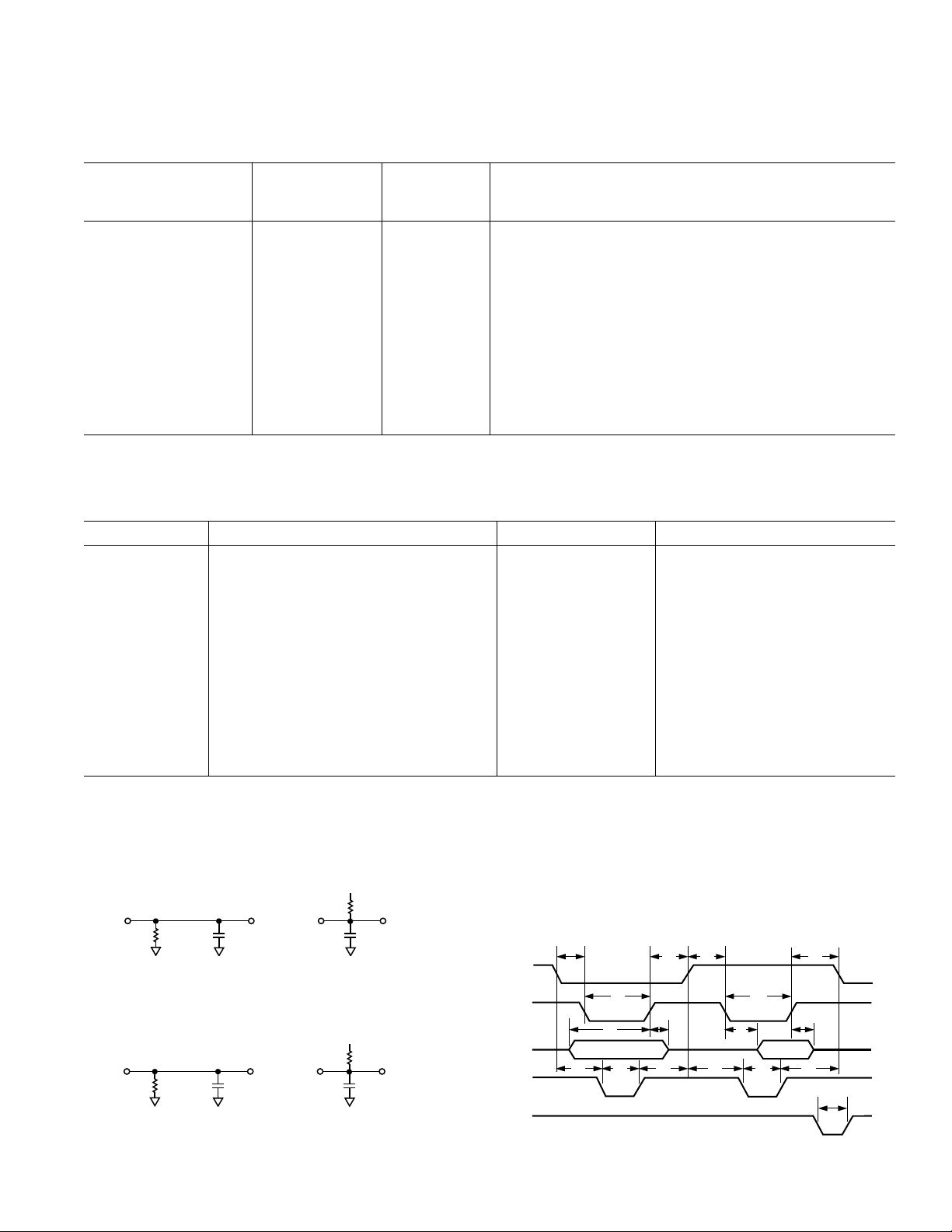
t6 is measured with the load circuits of Figure 1 and defined as the time required for an output to cross 0.8 V or 2.4 V.
3
t7 is defined as the time required for an output to change 0.5 V when loaded with the circuits of Figure 2.
Specifications subject to change without notice.
DBN
3k⍀
a. High Z to V
Figure 1. Load Circuits for Access Time (t6)
DBN
a. V
3k⍀
to High Z
OH
0 ns min CLR Setup Time
70 ns min CLR Pulsewidth
0 ns min CLR Hold Time
70 ns min LDAC Pulsewidth
130 ns min CS Pulsewidth (Read Cycle)
5V
3k⍀
100pF
DGND
5V
3k⍀
10pF
DGND
to High Z
OL
R/ W
OL
CS
DATA
CLR
LDAC
DGND
DGND
OH
100pF
DBN
b. High Z to V
DBN
10pF
b. V
= +5 V; VDD= +14.25 V to +15.75 V; VSS= –14.25 V
REF+
= 0 V, V
= V
REF–
t
1
t
8
loaded. V
OUT
loaded. V
OUT
unloaded.
OUT
= 1 V rms, 10 kHz sine wave.
REF+
. DAC loaded with 0111011 . . . 11.
OUT
= 0 V.
t
3
t
2
t
4
t
9
t
5
t
10
= 0 V. Typically 3.5 µs.
REF–
= –5 V. Typically 6.5 µs.
REF–
t
1
t
12
t
6
DATA VALIDDATA VALID
t
t
t
9
8
9
Figure 3. Timing DiagramFigure 2. Load Circuits for Bus Relinquish Time (t7)
t
3
t
7
t
10
t
11
5V
0V
5V
0V
5V
0V
5V
0V
5V
0V
REV. E
–3–
AD7846
ABSOLUTE MAXIMUM RATINGS
1
VDD to DGND . . . . . . . . . . . . . . . . . . . . . . . . . –0.4 V to +17 V
V
to DGND . . . . . . . . . . . . . . . –0.4 V, VDD + 0.4 V or +7 V
CC
(Whichever Is Lower)
to DGND . . . . . . . . . . . . . . . . . . . . . . . . . +0.4 V to –17 V
V
SS
V
to DGND . . . . . . . . . . . . . . . . VDD + 0.4 V, VSS – 0.4 V
REF+
to DGND . . . . . . . . . . . . . . . . VDD + 0.4 V, VSS – 0.4 V
V
REF–
V
to DGND2 . . . . . . . . VDD + 0.4 V, VSS – 0.4 V or ±10 V
OUT
NOTES
1
Stresses above those listed under Absolute Maximum Ratings may cause perma-
nent damage to the device. This is a stress rating only; functional operation of the
device at these or any other conditions above those indicated in the operational
sections of this specification is not implied. Exposure to absolute maximum rating
conditions for extended periods may affect device reliability. Only one Absolute
Maximum Rating may be applied at any one time.
2
V
may be shorted to DGND, VDD, VSS, VCC provided that the power dissipation
OUT
of the package is not exceeded.
(Whichever Is Lower)
to DGND . . . . . . . . . . . . . . . . . . VDD + 0.4 V, VSS – 0.4 V
R
IN
Digital Input Voltage to DGND . . . . . . –0.4 V to V
Digital Output Voltage to DGND . . . . . –0.4 V to V
+ 0.4 V
CC
+ 0.4 V
CC
Power Dissipation (Any Package)
To +75°C . . . . . . . . . . . . . . . . . . . . . . . . . . . . . . 1000 mW
Derates above +75°C . . . . . . . . . . . . . . . . . . . . . 10 mW/°C
Operating Temperature Range
J, K Versions . . . . . . . . . . . . . . . . . . . . . . . . . 0°C to +70°C
A, B Versions . . . . . . . . . . . . . . . . . . . . . . . –25°C to +85°C
Storage Temperature Range . . . . . . . . . . . . –65°C to +150°C
Lead Temperature (Soldering) . . . . . . . . . . . . . . . . . . +300°C
ORDERING GUIDE
Model Temperature Range Relative Accuracy Package Description Package Options
AD7846JN 0°C to +70°C ±16 LSB Plastic DIP N-28A
AD7846KN 0°C to +70°C ±8 LSB Plastic DIP N-28A
AD7846JP 0°C to +70°C ±16 LSB Plastic Leaded Chip Carrier (PLCC) P-28A
AD7846KP 0°C to +70°C ±8 LSB Plastic Leaded Chip Carrier (PLCC) P-28A
AD7846AP –40°C to +85°C ± 16 LSB Plastic Leaded Chip Carrier (PLCC) P-28A
AD7846AQ –40°C to +85°C ±16 LSB Ceramic DIP Q-28
AD7846BP –40°C to +85°C ±8 LSB Plastic Leaded Chip Carrier (PLCC) P-28A
CAUTION
ESD (electrostatic discharge) sensitive device. The digital control inputs are diode protected;
however, permanent damage may occur on unconnected devices subject to high energy electrostatic fields. Unused devices must be stored in conductive foam or shunts. The protective foam
should be discharged to the destination socket before devices are removed.
TERMINOLOGY
LEAST SIGNIFICANT BIT
This is the analog weighting of 1 bit of the digital word in a DAC.
For the AD7846, 1 LSB = (V
REF+–VREF–
)/216.
Relative Accuracy
Relative accuracy or endpoint nonlinearity is a measure of the
maximum deviation from a straight line passing through the endpoints of the DAC transfer function. It is measured after adjusting for both endpoints (i.e., offset and gain errors are adjusted
out) and is normally expressed in least significant bits or as a
percentage of full-scale range.
Differential Nonlinearity
Differential nonlinearity is the difference between the measured
change and the ideal change between any two adjacent codes. A
specified differential nonlinearity of ±1 LSB over the operating
temperature range ensures monotonicity.
Gain Error
Gain error is a measure of the output error between an ideal
DAC and the actual device output with all 1s loaded after offset
error has been adjusted out. Gain error is adjustable to zero
with an external potentiometer.
Offset Error
This is the error present at the device output with all 0s loaded
in the DAC. It is due to op amp input offset voltage and bias
current and the DAC leakage current.
Bipolar Zero Error
When the AD7846 is connected for bipolar output and 10 . . . 000
is loaded to the DAC, the deviation of the analog output from the
ideal midscale of 0 V is called the bipolar zero error.
Digital-to-Analog Glitch Impulse
This is the amount of charge injected from the digital inputs to
the analog output when the inputs change state. This is normally
specified as the area of the glitch in either pA-secs or nV-secs
depending upon whether the glitch is measured as a current or a
voltage.
Multiplying Feedthrough Error
This is an ac error due to capacitive feedthrough from either of
the V
terminals to V
REF
when the DAC is loaded with all 0s.
OUT
Digital Feedthrough
When the DAC is not selected (i.e., CS is held high), high frequency logic activity on the digital inputs is capacitively coupled
through the device to show up as noise on the V
noise is digital feedthrough.
–4–
WARNING!
ESD SENSITIVE DEVICE
pin. This
OUT
REV. E
AD7846
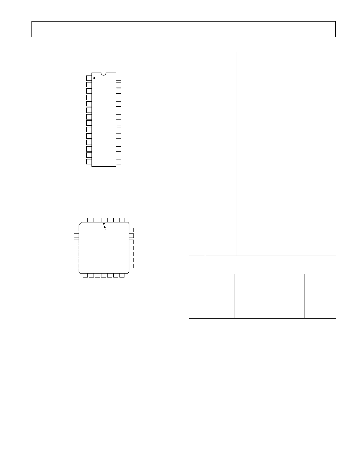
PIN CONFIGURATIONS
DIP
DB2
1
DB1
2
DB0
3
V
4
DD
V
5
OUT
R
6
IN
SS
AD7846
7
TOP VIEW
(Not to Scale)
8
9
10
11
12
13
14
V
REF+
V
REF–
DB15
DB14
DB13
DB12
DB11
V
PLCC
DD
V
DB0
DB1
DB2
V
V
REF+
V
REF–
DB15
DB14
4 3 2 1 28 27 26
5
OUT
6
R
IN
7
8
9
V
SS
10
11
12 13 14 15 16 17 18
DB13
DB12
PIN 1
IDENTIFIER
AD7846
TOP VIEW
(Not to Scale)
DB11
DB10
DB3
DB9
28
27
26
25
24
23
22
21
20
19
18
17
16
15
DB4
DB8
DB3
DB4
DB5
LDAC
CLR
CS
R/W
V
CC
DGND
DB6
DB7
DB8
DB9
DB10
DB5
DB7
25
24
23
22
21
20
19
LDAC
CLR
CS
R/W
V
CC
DGND
DB6
PIN FUNCTION DESCRIPTION
Pin Mnemonic Description
1–3 DB2–DB0 Data I/O pins. DB0 is LSB.
4V
DD
Positive supply for analog circuitry. This is
+15 V nominal.
5V
6R
OUT
IN
DAC output voltage pin.
Input to summing resistor of DAC output
amplifier. This is used to select output
voltage ranges. See Table I.
7V
REF+
V
Input. The DAC is specified for V
REF+
REF+
= +5 V.
8V
REF–
V
Input. For unipolar operation con-
REF–
nect V
to 0 V and for bipolar operation
REF–
connect it to –5 V. The device is specified
for both conditions.
9V
SS
Negative supply for the analog circuitry.
This is –15 V nominal.
10–19 DB15–DB6 Data I/O pins. DB15 is MSB.
20 DGND Ground pin for digital circuitry.
21 V
CC
Positive supply for digital circuitry. This is
+5 V nominal.
22 R/W R/W input. This can be used to load data to
the DAC or to read back the DAC latch
contents.
23 CS Chip select input. This selects the device.
24 CLR Clear input. The DAC can be cleared to
000 . . . 000 or 100 . . . 000. See Table II.
25 LDAC Asynchronous load input to DAC.
26–28 DB5–DB3 Data I/O pins.
Table I. Output Voltage Ranges
Output Range V
REF+
0 V to +5 V +5 V 0 V V
V
REF–
R
IN
OUT
0 V to +10 V +5 V 0 V 0 V
+5 V to –5 V +5 V –5 V V
OUT
+5 V to –5 V +5 V 0 V +5 V
+10 V to –10 V +5 V –5 V 0 V
REV. E
–5–
 Loading...