LC2MOS
VDDV
FEATURES
16-bit monotonicity over temperature
±2 LSBs integral linearity error
Microprocessor compatible with readback capability
Unipolar or bipolar output
Multiplying capability
Low power (100 mW typical)
GENERAL DESCRIPTION
The AD7846 is a 16-bit DAC constructed with the Analog Devices,
2
Inc., LC
and an on-chip output amplifier. These can be configured to
give a unipolar output range (0 V to +5 V, 0 V to +10 V) or
bipolar output ranges (±5 V, ±10 V).
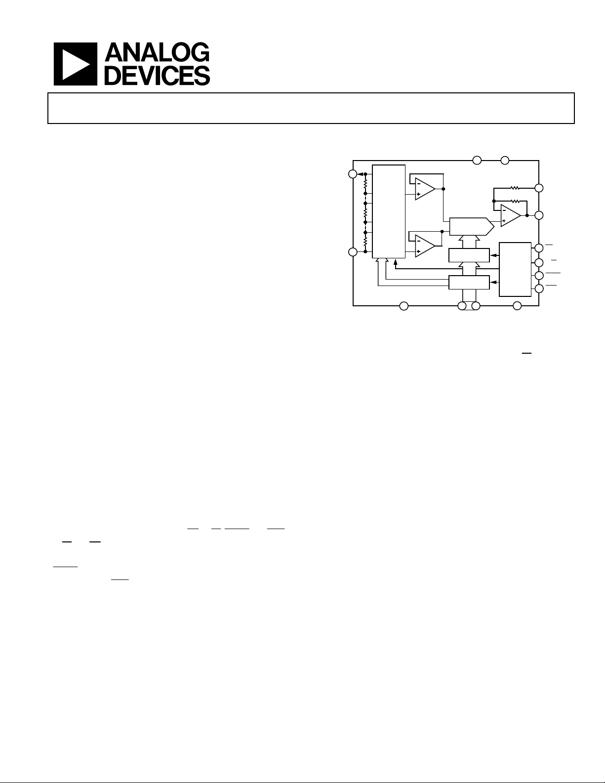
The DAC uses a segmented architecture. The four MSBs in the
DAC latch select one of the segments in a 16-resistor string.
Both taps of the segment are buffered by amplifiers and fed to a
12-bit DAC, which provides a further 12 bits of resolution. This
architecture ensures 16-bit monotonicity. Excellent integral
linearity results from tight matching between the input offset
voltages of the two buffer amplifiers.
In addition to the excellent accuracy specifications, the AD7846
also offers a comprehensive microprocessor interface. There are
16 data I/O pins, plus control lines (
R/
This is the readback function, which is useful in ATE applications.
LDAC
system and the
MOS process. It has V
W
and CS allow writing to and reading from the I/O latch.
REF+
and V
CS
reference inputs
REF−
LDAC
, R/W,
and
allows simultaneous updating of DACs in a multi-DAC
CLR
line will reset the contents of the DAC latch
CLR
).
16-Bit Voltage Output DAC
AD7846
FUNCTIONAL BLOCK DIAGRAM
CC
21 4
V
7
REF+
V
REF–
R
16
SEGMENT
R
SWITCH
MATRIX
R
8
4
A2
A1
9
V
SS
to 00…000 or 10…000 depending on the state of R/
means that the DAC output can be reset to 0 V in both the
unipolar and bipolar configurations.
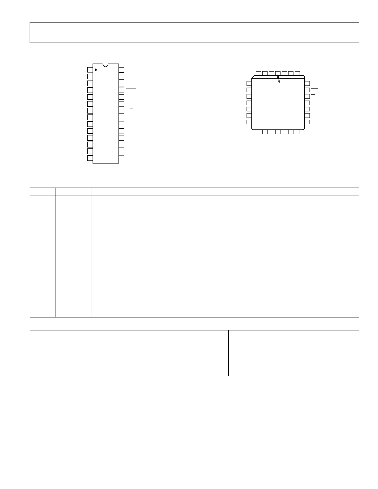
The AD7846 is available in 28-lead plastic, ceramic, and PLCC
packages.
PRODUCT HIGHLIGHTS
1. 16-Bit Monotonicity
The guaranteed 16-bit monotonicity over temperature
makes the AD7846 ideal for closed-loop applications.
2. Readback
The ability to read back the DAC register contents
minimizes software routines when the AD7846 is used in
ATE systems.
3. Power Dissipation
Power dissipation of 100 mW makes the AD7846 the
lowest power, high accuracy DAC on the market.
AD7846
12-BIT DAC
DAC LATCH
I/O LATCH
10 3 20
DB15 DB0
Figure 1.
R
6
R
W
V
5
23
CS
22
R/W
25
LDAC
24
CLR
. This
IN
OUT
R
A3
12
12
CONTROL
LOGIC
DGND
08490-001
Rev. G
Information furnished by Analog Devices is believed to be accurate and reliable. However, no
responsibility is assumed by Analog Devices for its use, nor for any infringements of patents or other
rights of third parties that may result from its use. Specifications subject to change without notice. No
license is granted by implication or otherwise under any patent or patent rights of Analog Devices.
Trademarks and registered trademarks are the property of their respective owners.
One Technology Way, P.O. Box 9106, Norwood, MA 02062-9106, U.S.A.
Tel: 781.329.4700 www.analog.com
Fax: 781.461.3113 ©2000–2010 Analog Devices, Inc. All rights reserved.

AD7846
TABLE OF CONTENTS
Features .............................................................................................. 1
Functional Block Diagram .............................................................. 1
General Description ......................................................................... 1
Product Highlights ........................................................................... 1
Revision History ............................................................................... 2
Specifications ..................................................................................... 3
AC Performance Characteristics ................................................ 4
Timing Characteristics ................................................................ 5
Absolute Maximum Ratings ............................................................ 6
ESD Caution .................................................................................. 6
Pin Configurations and Function Descriptions ........................... 7
Typical Performance Characteristics ............................................. 8
Terminology .................................................................................... 10
Circuit Description ......................................................................... 11
Digital Section ............................................................................. 11
Digital-to-Analog Conversion .................................................. 11
Output Stage ................................................................................ 12
Unipolar Binary Operation ........................................................... 13
Bipolar Operation ........................................................................... 14
Multiplying Operation ............................................................... 14
Position Measurement Application .............................................. 15
Microprocessor Interfacing ........................................................... 16
AD7846-to-8086 Interface ........................................................ 16
AD7846-to-MC68000 Interface ............................................... 16
Digital Feedthrough ....................................................................... 17
Application Hints ........................................................................... 18
Noise ............................................................................................ 18
Grounding ................................................................................... 18
Printed Circuit Board Layout ................................................... 18
Outline Dimensions ....................................................................... 20
Ordering Guide .......................................................................... 22
REVISION HISTORY
4/10—Rev. F to Rev. G
Change to Figure 1 ........................................................................... 1
12/09—Rev. E to Rev. F
Updated Format .................................................................. Universal
Changes to Table 4 ............................................................................ 6
Deleted Other Output Voltage Ranges Section ............................ 9
Deleted Figure 20 and Table 5; Renumbered Sequentially ......... 9
Deleted Test Application Section and Figure 21 ........................ 10
Deleted Figure 29 to Figure 31 ...................................................... 14
Changes to Printed Circuit Board Layout Section ..................... 18
Updated Outline Dimensions ....................................................... 20
Changes to Ordering Guide .......................................................... 22
Rev. G | Page 2 of 24

AD7846
SPECIFICATIONS
VDD = +14.25 V to +15.75 V; VSS = −14.25 V to –15.75 V; VCC = +4.75 V to +5.25 V. V
R
connected to 0 V. All specifications T
IN
MIN
to T
, unless otherwise noted.
MAX
Table 1.
Parameter1 J, A Versions K, B Versions Unit Test Conditions/Comments
RESOLUTION 16 16 Bits
UNIPOLAR OUTPUT V
Relative Accuracy at +25°C ±12 ±4 LSB typ 1 LSB = 153 V
T
to T
MIN
±16 ±8 LSB max
MAX
Differential Nonlinearity Error ±1 ±0.5 LSB max All grades guaranteed monotonic
Gain Error at +25°C ±12 ±6 LSB typ V
T
to T
MIN
±16 ±16 LSB max
MAX
Offset Error at +25°C ±12 ±6 LSB typ
T
to T
MIN
±16 ±16 LSB max
MAX
Gain TC2 ±1 ±1 ppm FSR/°C typ
Offset TC2 ±1 ±1 ppm FSR/°C typ
BIPOLAR OUTPUT V
Relative Accuracy at +25°C ±6 ±2 LSB typ 1 LSB = 305 V
T
to T
MIN
±8 ±4 LSB max
MAX
Differential Nonlinearity Error ±1 ±0.5 LSB max All grades guaranteed monotonic
Gain Error at +25°C ±6 ±4 LSB typ V
T
to T
MIN
±16 ±16 LSB max
MAX
Offset Error at +25°C ±6 ±4 LSB typ V
T
to T
MIN
±16 ±12 LSB max
MAX
Bipolar Zero Error at +25°C ±6 ±4 LSB typ
T
to T
MIN
±12 ±8 LSB max
MAX
Gain TC2 ±1 ±1 ppm FSR/°Ctyp
Offset TC2 ±1 ±1 ppm FSR/°Ctyp
Bipolar Zero TC2 ±1 ±1 ppm FSR/°Ctyp
REFERENCE INPUT
Input Resistance 20 20 kΩ min Resistance from V
40 40 kΩ max Typically 30 kΩ
V
Range VSS + 6 to VSS + 6 to V min to
REF+
V
V
Range VSS + 6 to VSS + 6 to V min to
REF−
V
OUTPUT CHARACTERISTICS
Output Voltage Swing
− 6 VDD − 6 V max
DD
− 6 VDD − 6 V max
DD
V
+ 4 to VSS + 4 to
SS
V
− 3 VDD − 3
DD
V max
Resistive Load 2 2 kΩ min To 0 V
Capacitive Load 1000 1000 pF max To 0 V
Output Resistance 0.3 0.3 Ω typ
Short Circuit Current ±25 ±25 mA typ To 0 V or any power supply
DIGITAL INPUTS
VIH (Input High Voltage) 2.4 2.4 V min
VIL (Input Low Voltage) 0.8 0.8 V max
IIN (Input Current) ±10 ±10 A max
CIN (Input Capacitance)2 10 10 pF max
loaded with 2 kΩ, 1000 pF to 0 V; V
OUT
= 0 V, V
REF−
load = 10 MΩ
OUT
= –5 V, V
REF−
load = 10 MΩ
OUT
load = 10 MΩ
OUT
= 0 V to +10 V
OUT
= −10 V to +10 V
OUT
REF+
to V
REF+
REF−
= +5 V;
Rev. G | Page 3 of 24
AD7846
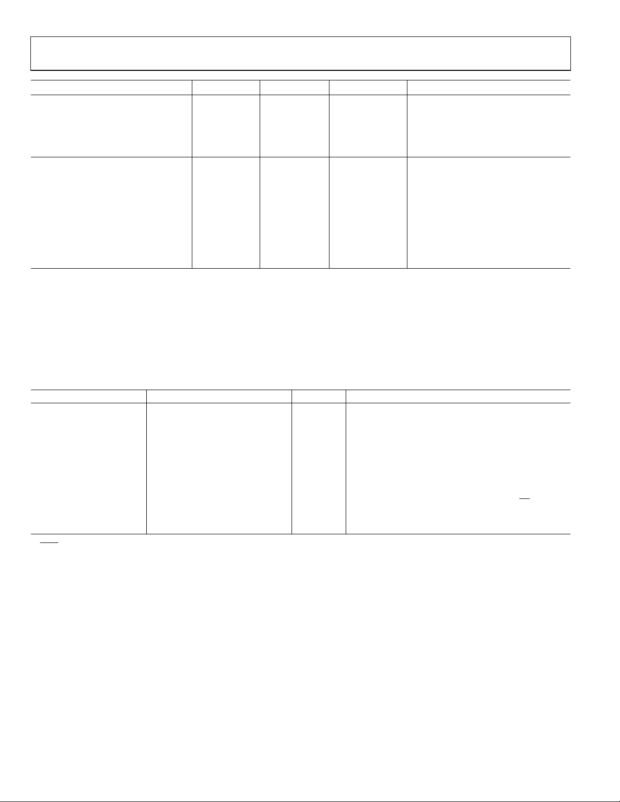
Parameter1 J, A Versions K, B Versions Unit Test Conditions/Comments
DIGITAL OUTPUTS
VOL (Output Low Voltage) 0.4 0.4 V max I
VOH (Output High Voltage) 4.0 4.0 V min I
Floating State Leakage Current ±10 ±10 A max DB0 to DB15 = 0 to VCC
Floating State Output Capacitance2 10 10 pF max
POWER REQUIREMENTS3
VDD +11.4/+15.75 +11.4/+15.75 V min/V max
VSS −11.4/−15.75 −11.4/−15.75 V min/V max
VCC +4.75/+5.25 +4.75/+5.25 V min/V max
IDD 5 5 mA max V
ISS 5 5 mA max V
ICC 1 1 mA max
Power Supply Sensitivity4 1.5 1.5 LSB/V max
Power Dissipation 100 100 mW typ V
1
Temperature ranges as follows: J, K versions: 0°C to +70°C; A, B versions: −40°C to +85°C.
2
Guaranteed by design and characterization, not production tested.
3
The AD7846 is functional with power supplies of ±12 V. See the Typical Performance Characteristics section.
4
Sensitivity of gain error, offset error, and bipolar zero error to VDD, VSS variations.
AC PERFORMANCE CHARACTERISTICS
These characteristics are included for design guidance and are not subject to test. V
to −15.75 V; V
= +4.75 V to +5.25 V; RIN connected to 0 V, unless otherwise noted.
CC
= +5 V; VDD = +14.25 V to +15.75 V; VSS = −14.25 V
REF+
= 1.6 mA
SINK
= 400 A
SOURCE
unloaded
OUT
unloaded
OUT
unloaded
OUT
Table 2.
Parameter Limit at T
MIN
to T
(All Versions) Unit Test Conditions/Comments
MAX
Output Settling Time1 6 s max To 0.006% FSR, V
9 s max To 0.003% FSR, V
Slew Rate 7 V/s typ
Digital-to-Analog Glitch
Impulse 70 nV-sec typ
AC Feedthrough 0.5 mV p-p typ
DAC alternately loaded with 10…0000 and 01…1111,
V
unloaded
OUT
= 0 V, V
V
REF−
REF+
with all 0s
Digital Feedthrough 10 nV-sec typ
Output Noise Voltage
50 nV/√Hz typ
Density, 1 kHz to 100 kHz
1
LDAC
= 0. Settling time does not include deglitching time of 2.5 µs (typ).
DAC alternately loaded with all 1s and all 0s. CS
Measured at V
V
= V
REF+
REF−
OUT
= 0 V
loaded, V
OUT
loaded, V
OUT
= 0 V, typically 3.5 s
REF−
= –5 V, typically 6.5 s
REF−
= 1 V rms, 10 kHz sine wave, DAC loaded
high
, DAC loaded with 0111011…11,
Rev. G | Page 4 of 24
AD7846
V
V
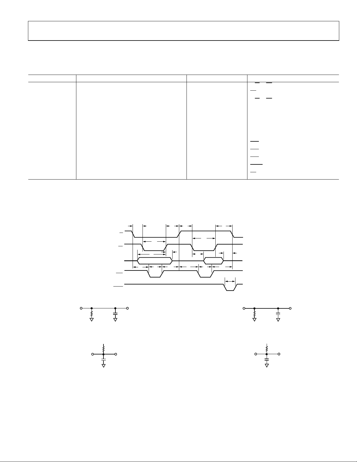
TIMING CHARACTERISTICS
VDD = +14.25 V to +15.75 V, VSS = −14.25 V to −15.75 V, VCC = +4.75 V to +5.25 V, unless otherwise noted.
Table 3.
Parameter1 Limit at T
t1
t2
t3
0 ns min
60 ns min
0 ns min
t4 60 ns min Data setup time
t5 0 ns min Data hold time
2
t
120 ns max Data access time
6
3
t
10 ns min Bus relinquish time
7
60 ns max
t8
t9
t10
t11
t12
1
Timing specifications are sample tested at +25°C to ensure compliance. All input control signals are specified with tR = tF = 5 ns (10% to 90% of +5 V) and timed from a
voltage level of 1.6 V.
2
t6 is measured with the load circuits of Figure 3 and Figure 4 and defined as the time required for an output to cross 0.8 V or 2.4 V.
3
t7 is defined as the time required for an output to change 0.5 V when loaded with the circuits of Figure 5 and Figure 6.
0 ns min
70 ns min
0 ns min
70 ns min
130 ns min
DBn
Figure 3. Load Circuit for Access Time (t
3kΩ
MIN
DGND
to T
(All Versions) Unit Test Conditions/Comments
MAX
to CS setup time
R/W
pulse width (write cycle)
CS
to CS hold time
R/W
setup time
CLR
pulse width
CLR
hold time
CLR
pulse width
LDAC
pulse width (read cycle)
CS
R/W
CS
DB0
TO
DB15
CLR
LDAC
t
1
t
t
4
t
8
t
3t1
t
2
t
5
t
t
10
9
12
t
6
t
t
8
t
3
t
DATA VALIDDATA VALID
t
10
9
5V
0V
5V
0V
7
5V
0V
5V
0V
t
11
5V
0V
8490-006
Figure 2. Timing Diagram
100pF
8490-002
)—High Z to VOH
6
Figure 5. Load Circuit for Access Time (t
DBn
3kΩ
DGND
10pF
08490-004
)—High Z to VOH
7
5
DBn
3kΩ
100pF
DGND
08490-003
Figure 4. Load Circuits for Bus Relinquish Time (t
)—High Z to V
6
DBn
OL
Figure 6. Load Circuits for Bus Relinquish Time (t
5
3kΩ
10pF
DGND
08490-005
7
)—High Z to V
OL
Rev. G | Page 5 of 24
AD7846
ABSOLUTE MAXIMUM RATINGS
Table 4.
Parameter Rating
VDD to DGND −0.4 V to +17 V
VCC to DGND −0.4 V, VDD + 0.4 V, or +7 V
(whichever is lower)
VSS to DGND +0.4 V to −17 V
V
to DGND VDD + 0.4 V, VSS − 0.4 V
REF+
V
to DGND VDD + 0.4 V, VSS − 0.4 V
REF−
V
to DGND1 V
OUT
+ 0.4 V, VSS − 0.4 V, or ±10 V
DD
(whichever is lower)
RIN to DGND VDD + 0.4 V, VSS − 0.4 V
Digital Input Voltage to DGND −0.4 V to VCC + 0.4 V
Digital Output Voltage to DGND −0.4 V to VCC + 0.4 V
Power Dissipation (Any Package)
To +75°C 1000 mW
Derates above +75°C 10 mW/°C
Operating Temperature Range
J, K Versions 0°C to +70°C
A, B Versions −40°C to +85°C
Storage Temperature Range −65°C to +150°C
Lead Temperature (Soldering) +300°C
1
V
can be shorted to DGND, VDD, VSS, or VCC provided that the power
OUT
dissipation of the package is not exceeded.
Stresses above those listed under Absolute Maximum Ratings
may cause permanent damage to the device. This is a stress
rating only; functional operation of the device at these or any
other conditions above those indicated in the operational
section of this specification is not implied. Exposure to absolute
maximum rating conditions for extended periods may affect
device reliability.
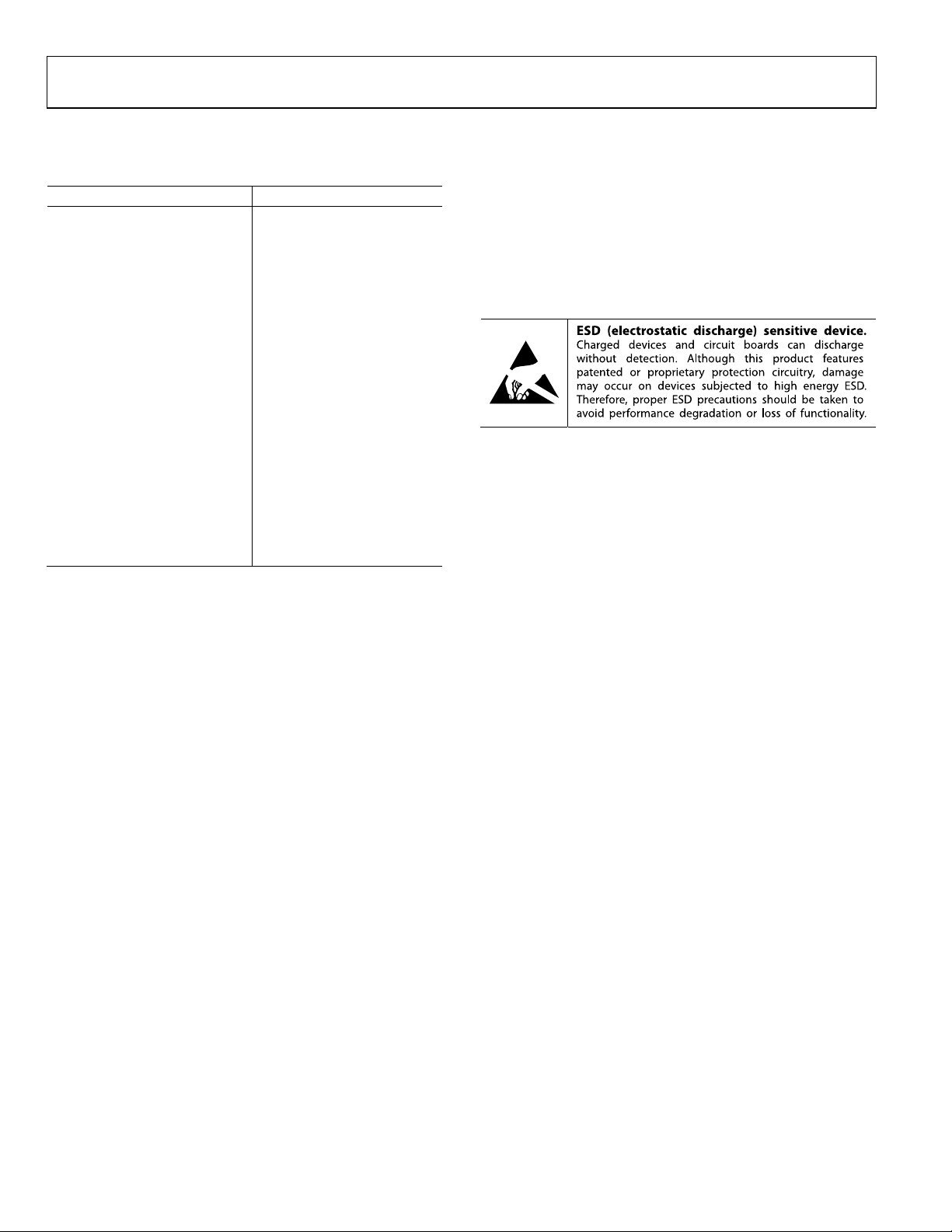
ESD CAUTION
Rev. G | Page 6 of 24
AD7846
V
V
PIN CONFIGURATIONS AND FUNCTION DESCRIPTIONS
VDDDB0
DB1
DB2
DB3
DB4
PIN 1
IDENTIFIER
DB9
DB8
DB5
DB7
25
24
23
22
21
20
19
LDAC
CLR
CS
R/W
V
CC
DGND
DB6
08490-008
DB2
DB1
DB0
V
V
OUT
R
REF+
REF–
V
DB15
DB14
DB13
DB12
DB11
DD
IN
SS
1
2
3
4
5
6
AD7846
7
TOP VIEW
(Not to Scale)
8
9
10
11
12
13
14
28
27
26
25
24
23
22
21
20
19
18
17
16
15
DB3
DB4
DB5
LDAC
CLR
CS
R/W
V
CC
DGND
DB6
DB7
DB8
DB9
DB10
V
V
REF+
V
REF–
DB15
DB14
08490-007
Figure 7. PDIP Pin Configuration
Table 5. Pin Function Descriptions
Pin Mnemonic Description
1 to 3 DB2 to DB0 Data I/Os. DB0 is LSB.
4 VDD Positive Supply for Analog Circuitry. This is +15 V nominal.
5 V
6 R
7 V
8 V
DAC Output Voltage.
OUT
Input to Summing Resistor of DAC Output Amplifier. This is used to select output voltage ranges. See Table 6.
IN
V
REF+
REF−
Input. The DAC is specified for V
REF+
Input. For unipolar operation connect V
V
REF−
REF+
= +5 V.
to 0 V, and for bipolar operation connect it to −5 V. The device is
REF−
specified for both conditions.
9 VSS Negative Supply for the Analog Circuitry. This is −15 V nominal.
10 to 19 DB15 to DB6 Data I/Os. DB15 is MSB.
20 DGND Ground for Digital Circuitry.
21 VCC Positive Supply for Digital Circuitry. This is +5 V nominal.
22
23
24
25
R/W Input. This pin can be used to load data to the DAC or to read back the DAC latch contents.
R/W
CS
CLR
LDAC
Chip Select Input. This pin selects the device.
Clear Input. The DAC can be cleared to 000…000 or 100…000. See Table 7.
Asynchronous Load Input to DAC.
26 to 28 DB5 to DB3 Data I/Os.
4 3 2 1 28 27 26
5
OUT
6
R
IN
7
8
9
V
SS
10
11
AD7846
TOP VIEW
(Not to Scale)
12 13 14 15 16 17 18
DB13
DB12
DB11
DB10
Figure 8. CERDIP Pin Configuration
Table 6. Output Voltage Ranges
Output Range V
0 V to +5 V +5 V 0 V V
V
REF+
R
REF−
IN
OUT
0 V to +10 V +5 V 0 V 0 V
+5 V to −5 V +5 V −5 V V
OUT
+5 V to −5 V +5 V 0 V +5 V
+10 V to −10 V +5 V −5 V 0 V
Rev. G | Page 7 of 24
AD7846
TYPICAL PERFORMANCE CHARACTERISTICS
–0.40VA1
1V 2mV 20µs
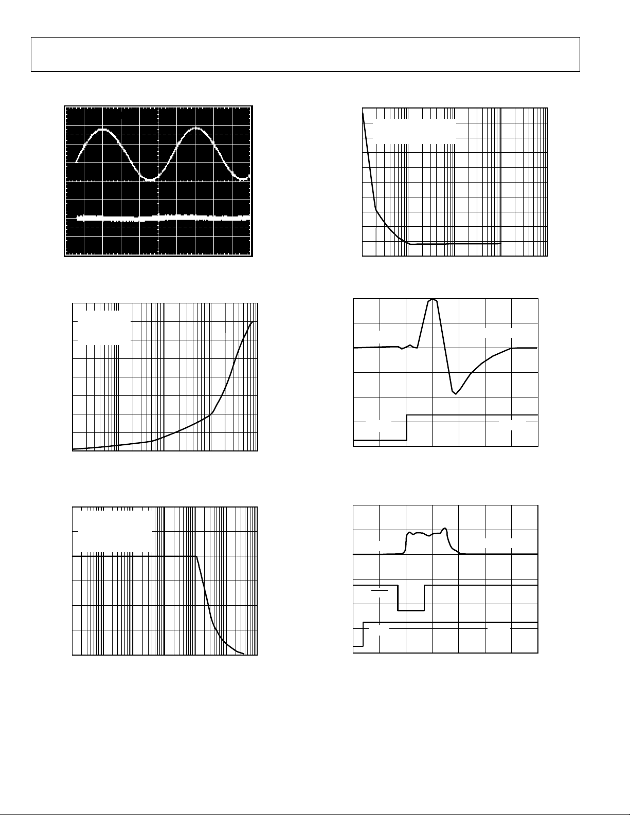
Figure 9. AC Feedthrough, V
8
VDD = +15V
7
V
= –15V
SS
= +1V rms
+
V
REF
V
= 0V
–
6
REF
5
= 1 V rms, 10 kHz Sine Wave
REF+
08490-009
500
450
V
= V
REF–
= 0V
FREQUENCY (Hz)
REF+
GAIN = +1
400
DAC LOADED WIT H ALL 1s
350
300
250
200
150
100
NOISE SPECTRAL DENSITY (nV/√Hz)
50
0
100 1k 10k 100k 1M
Figure 12. Noise Spectral Density
V
OUT
50mV/DIV
08490-012
4
(mV p-p)
OUT
3
V
2
1
0
100
Figure 10. AC Feedthrough to V
30
VDD = +15V
V
SS
V
25
REF+
V
REF–
GAIN = +2
20
15
(V p-p)
OUT
V
10
5
0
10 100 1k 10k 100k 1M 10M
1k 10k 100k 1M
FREQUENCY (Hz)
vs. Frequency
OUT
= –15V
= ±5V SINE WAVE
= 0V
FREQUENCY (Hz)
DATA
0.5µs/DIV
08490-010
5V/DIV
8490-013
Figure 13. Digital-to-Analog Glitch Impulse Without Internal Deglitcher
(10…000 to 011…111 Transition)
V
OUT
LDAC
DATA
1µs/DIV
08490-011
50mV/DIV
5V/DIV
5V/DIV
8490-014
Figure 11. Large Signal Frequency Response
Figure 14. Digital-to-Analog Glitch Impulse with Internal Deglitcher
(10…000 to 011…111 Transition)
Rev. G | Page 8 of 24
 Loading...