ANALOG DEVICES AD7322 Service Manual
2-Channel, Software-Selectable, True
V
V
Bipolar Input, 1 MSPS, 12-Bit Plus Sign ADC
FEATURES
12-bit plus sign SAR ADC
True bipolar input ranges
Software-selectable input ranges
±10 V, ±5 V, ±2.5 V, 0 V to +10 V
1 MSPS throughput rate
Two analog input channels with channel sequencer
Single-ended, true differential, and pseudo differential
analog input capability
High analog input impedance
Low power: 21 mW
Full power signal bandwidth: 22 MHz
Internal 2.5 V reference
High speed serial interface
Power-down modes
14-lead TSSOP package
iCMOS process technology
GENERAL DESCRIPTION
The AD73221 is a 2-channel, 12-bit plus sign, successive approximation analog-to-digital converter (ADC) designed on the
iCMOS™ (industrial CMOS) process. iCMOS is a process
combining high voltage silicon with submicron CMOS and
complementary bipolar technologies. It enables the development of a wide range of high performance analog ICs capable of
33 V operation in a footprint that no previous generation of high
voltage parts could achieve. Unlike analog ICs using conventional
CMOS processes, iCMOS components can accept bipolar input
signals while providing increased performance, dramatically
reduced power consumption, and reduced package size.
The AD7322 can accept true bipolar analog input signals. The
AD7322 has four software-selectable input ranges, ±10 V, ±5 V,
±2.5 V, and 0 V to +10 V. Each analog input channel can be
independently programmed to one of the four input ranges.
The analog input channels on the AD7322 can be programmed
to be single-ended, true differential, or pseudo differential.
The ADC contains a 2.5 V internal reference. The AD7322 also
allows for external reference operation. If a 3 V reference is
applied to the REFIN/OUT pin, the AD7322 can accept a true
bipolar ±12 V analog input. Minimum ±12 V V
supplies are required for the ±12 V input range. The ADC has a
high speed serial interface that can operate at throughput rates
up to 1 MSPS.
1
Protected by U.S. Patent No. 6,731,232.
and VSS
DD
AD7322
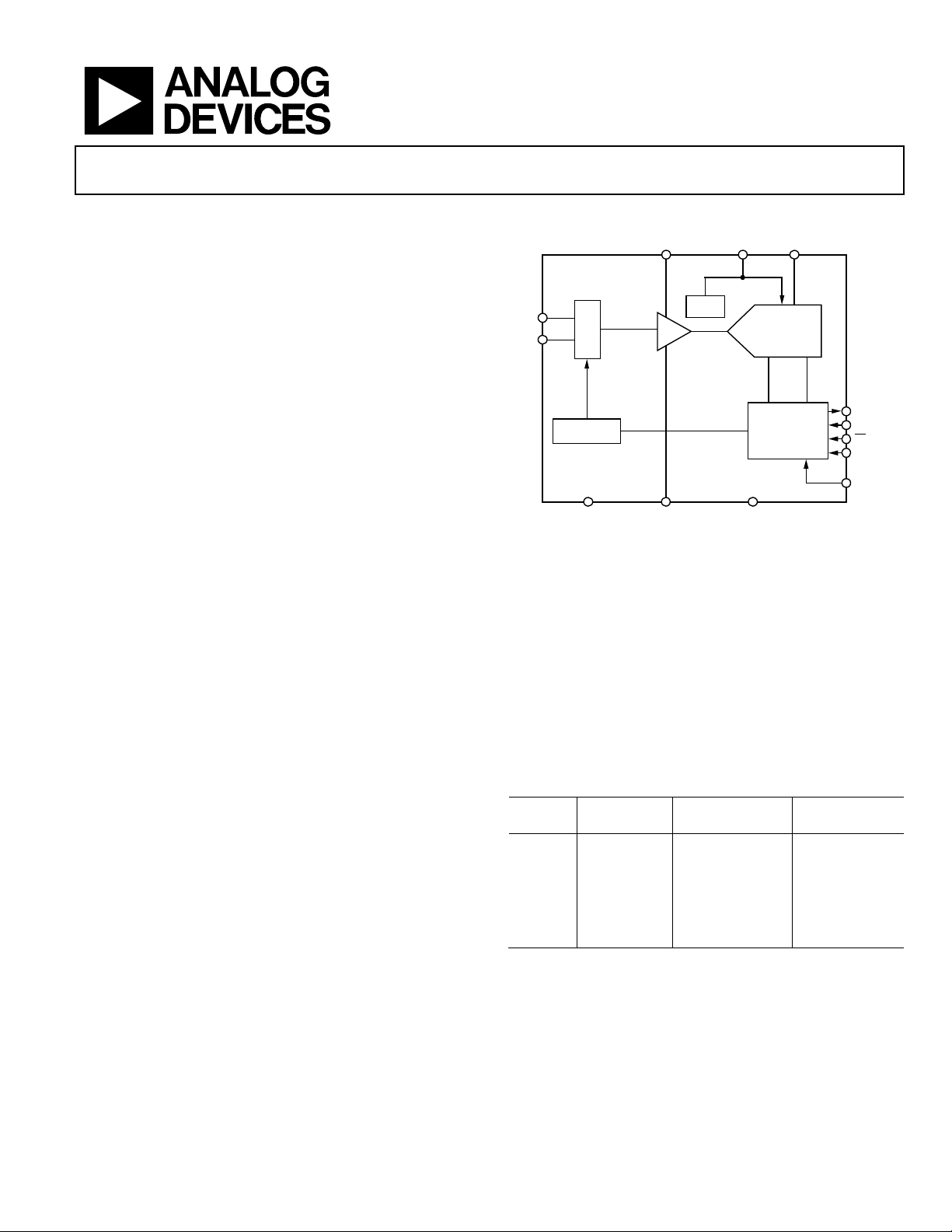
FUNCTIONAL BLOCK DIAGRAM
2.5V
VREF
Figure 1.
REFIN/OUT
SUCCESSIVE
APPROXIMATION
CONTROL LO GIC
AND REGIST ERS
DGND
13-BIT
ADC
CC
Number of
Channels
DOUT
SCLK
CS
DIN
V
DRIVE
DD
AD7322
VIN0
VIN1
I/P
MUX
CHANNEL
SEQUENCER
AGND V
T/H
SS
PRODUCT HIGHLIGHTS
1. The AD7322 can accept true bipolar analog input signals,
±10 V, ±5 V, and ±2.5 V, and 0 V to +10 V unipolar signals.
2. The two analog inputs can be configured as two single-
ended inputs, one true differential input, or one pseudo
differential input.
3. 1 MSPS serial interface. SPI-/QSPI™-/DSP-/MICROWIRE™-
compatible interface.
4. Low power, 31 mW maximum, at 1 MSPS throughput rate.
5. Channel sequencer.
Table 1. Similar Devices
Device
Number
AD7329 1000 kSPS 12-bit plus sign 8
AD7328 1000 kSPS 12-bit plus sign 8
AD7327 500 kSPS 12-bit plus sign 8
AD7324 1000 kSPS 12-bit plus sign 4
AD7323 500 kSPS 12-bit plus sign 4
AD7321 500 kSPS 12-bit plus sign 2
Throughput
Rate Number of bits
04863-001
Rev. A
Information furnished by Analog Devices is believed to be accurate and reliable. However, no
responsibility is assumed by Analog Devices for its use, nor for any infringements of patents or other
rights of third parties that may result from its use. Specifications subject to change without notice. No
license is granted by implication or otherwise under any patent or patent rights of Analog Devices.
Trademarks and registered trademarks are the property of their respective owners.
One Technology Way, P.O. Box 9106, Norwood, MA 02062-9106, U.S.A.
Tel: 781.329.4700 www.analog.com
Fax: 781.461.3113 ©2005–2010 Analog Devices, Inc. All rights reserved.

AD7322
TABLE OF CONTENTS
Features .............................................................................................. 1
Control Register ......................................................................... 22
Functional Block Diagram .............................................................. 1
General Description ......................................................................... 1
Product Highlights ........................................................................... 1
Revision History ............................................................................... 2
Specifications ..................................................................................... 3
Timing Specifications .................................................................. 6
Absolute Maximum Ratings ............................................................ 7
ESD Caution .................................................................................. 7
Pin Configuration and Function Descriptions ............................. 8
Typical Performance Characteristics ............................................. 9
Terminology .................................................................................... 13
Theory of Operation ...................................................................... 15
Circuit Information .................................................................... 15
Converter Operation .................................................................. 15
Analog Input Structure .............................................................. 16
Range Register ............................................................................ 24
Sequencer Operation ..................................................................... 25
Reference ..................................................................................... 26
V
............................................................................................ 26
DRIVE
Modes of Operation ....................................................................... 27
Normal Mode (PM1 = PM0 = 0) ............................................. 27
Full Shutdown Mode (PM1 = PM0 = 1) ................................. 27
Autoshutdown Mode (PM1 = 1, PM0 = 0) ............................. 28
Autostandby Mode (PM1 = 0, PM0 = 1) ................................ 28
Power vs. Throughput Rate ....................................................... 29
Serial Interface ................................................................................ 30
Microprocessor Interfacing ........................................................... 31
AD7322 to ADSP-21xx .............................................................. 31
AD7322 to ADSP-BF53x ........................................................... 31
Application Hints ........................................................................... 32
Typical Connection Diagram ................................................... 18
Analog Input ............................................................................... 18
Driver Amplifier Choice ............................................................ 20
Registers ........................................................................................... 21
Addressing Registers .................................................................. 21
REVISION HISTORY
1/10—Rev. 0 to Rev. A
Changes to Power Requirements, Normal Mode (Operational),
I
and I
CC
Parameter, Table 2 ............................................................................. 5
Changes to Endnote 1, Table 4 ........................................................ 7
Changes to Table 6 .......................................................................... 15
Changes to Figure 25 and Figure 26 ............................................. 16
Changes to Figure 30 and Figure 31 ............................................. 17
Changes to Figure 33 and Figure 34 ............................................. 18
Changes to Figure 39 ...................................................................... 19
Parameter; and Power Dissipation, Normal Mode
DRIVE
Layout and Grounding .............................................................. 32
Power Supply Configuration .................................................... 32
Outline Dimensions ....................................................................... 33
Ordering Guide .......................................................................... 33
Changes to Figure 40 and Figure 41............................................. 20
Changes to Autostandby Mode (PM1 = 0, PM = 1) Section .... 28
Changes to Table 14 and Table 15 ................................................ 31
Added Power Supply Configuration Section .............................. 32
Added Table 16; Renumbered Sequentially ................................ 32
Added Figure 53; Renumbered Sequentially .............................. 32
Updated Outline Dimensions ....................................................... 33
12/05—Revision 0: Initial Version
Rev. A | Page 2 of 36
AD7322
SPECIFICATIONS
Unless otherwise noted, VDD = 12 V to 16.5 V, VSS = −12 V to −16.5 V, VCC = 4.75 V to 5.25 V, V
internal/external, f
= 20 MHz, fS = 1 MSPS, TA = T
SCLK
MAX
to T
; for VCC < 4.75 V, all specifications are typical.
MIN
Table 2.
B Version
Parameter1 Min Typ Max Unit Test Conditions/Comments
DYNAMIC PERFORMANCE fIN = 50 kHz sine wave
Signal-to-Noise Ratio (SNR)
72.5 dB Single-ended/pseudo differential mode
Signal-to-Noise + Distortion (SINAD)2 75 dB Differential mode; ±2.5 V and ±5 V ranges
76 dB Differential mode; 0 V to +10 V and ±10 V ranges
72 dB Single-ended/pseudo differential mode;
72.5 dB Single-ended/pseudo differential mode;
Total Harmonic Distortion (THD)2 −80 dB Differential mode; ±2.5 V and ±5 V ranges
−82 dB Differential mode; 0 V to +10 V and ±10 V ranges
−77 dB Single-ended/pseudo differential mode;
−80 dB Single-ended/pseudo differential mode;
Peak Harmonic or Spurious Noise
2
(SFDR)
−82 dB Differential mode; 0 V to +10 V and ±10 V ranges
−78 dB Single-ended/pseudo differential mode;
−79 dB Single-ended/pseudo differential mode;
Intermodulation Distortion (IMD)
Second-Order Terms −88 dB
Third-Order Terms
Aperture Delay
Aperture Jitter
Common-Mode Rejection Ratio
(CMRR)
3
3
2
Channel-to-Channel Isolation
Full Power Bandwidth
5 MHz At 0.1 dB
DC ACCURACY All dc accuracy specifications are typical for 0 V to
Single-ended/pseudo differential mode:
Differential mode: 1 LSB = FSR/8192; unless
Resolution 13 Bits
No Missing Codes 12-bit plus
11-bit plus
Integral Nonlinearity
−0.7/+1.2 LSB Single-ended/pseudo differential mode
2
76 dB Differential mode
−80 dB Differential mode; ±2.5 V and ±5 V ranges
2
fa = 50 kHz, fb = 30 kHz
−90 dB
7 ns
50 ps
−79 dB Up to 100 kHz ripple frequency; see Figure 17
2
−72 dB fIN on unselected channels up to 100 kHz; see Figure 14
22 MHz At 3 dB
Bits Differential mode
sign (13 bits)
Bits Single-ended/pseudo differential mode
sign (12 bits)
2
±1.1 LSB Differential mode
±1 LSB Single-ended/pseudo differential mode
= 2.7 V to 5.25 V, V
DRIVE
= 2.5 V to 3.0 V
REF
±2.5 V and ±5 V ranges
0 V to +10 V and ±10 V ranges
±2.5 V and ±5 V ranges
0 V to +10 V and ±10 V ranges
±2.5 V and ±5 V ranges
0 V to +10 V and ±10 V ranges
10 V mode
1 LSB = FSR/4096; unless otherwise noted
otherwise noted
(LSB = FSR/8192)
Rev. A | Page 3 of 36

AD7322
B Version
Parameter1 Min Typ Max Unit Test Conditions/Comments
Differential Nonlinearity2 −0.9/+1.5 LSB Differential mode; guaranteed no missing codes to
±0.9 LSB Single-ended mode; guaranteed no missing codes
−0.7/+1 LSB Single-ended/pseudo differential mode
Offset Error
2, 4
−4/+9 LSB Single-ended/pseudo differential mode
−7/+10 LSB Differential mode
Offset Error Match
2, 4
±0.6 LSB Single-ended/pseudo differential mode
±0.5 LSB Differential mode
Gain Error
2, 4
±8 LSB Single-ended/pseudo differential mode
±14 LSB Differential mode
Gain Error Match
2, 4
±0.5 LSB Single-ended/pseudo differential mode
±0.5 LSB Differential mode
Positive Full-Scale Error
2, 5
±4 LSB Single-ended/pseudo differential mode
±7 LSB Differential mode
Positive Full-Scale Error Match
2, 5
±0.5 LSB Single-ended/pseudo differential mode
±0.5 LSB Differential mode
Bipolar Zero Error
2, 5
±8.5 LSB Single-ended/pseudo differential mode
±7.5 LSB Differential mode
Bipolar Zero Error Match
2, 5
±0.5 LSB Single-ended/pseudo differential mode
±0.5 LSB Differential mode
Negative Full-Scale Error
2, 5
±4 LSB Single-ended/pseudo differential mode
±6 LSB Differential mode
Negative Full-Scale Error Match
2, 5
±0.5 LSB Single-ended/pseudo differential mode
±0.5 LSB Differential mode
ANALOG INPUT
Input Voltage Ranges Reference = 2.5 V; see Table 6
(Programmed via Range Register) ±10 V VDD = 10 V min, VSS = −10 V min, VCC = 2.7 V to 5.25 V
±5 V VDD = 5 V min, VSS = −5 V min, VCC = 2.7 V to 5.25 V
±2.5 V VDD = 5 V min, VSS = − 5 V min, VCC = 2.7 V to 5.25 V
0 to 10 V VDD = 10 V min, VSS = AGND min, VCC = 2.7 V to 5.25 V
Pseudo Differential VIN(−) Input
V
Range
±3.5 V Reference = 2.5 V; range = ±10 V
±6 V Reference = 2.5 V; range = ±5 V
±5 V Reference = 2.5 V; range = ±2.5 V
+3/−5 V Reference = 2.5 V; range = 0 V to +10 V
DC Leakage Current ±80 nA VIN = VDD or VSS
3 nA Per channel, VIN = VDD or VSS
Input Capacitance3 13.5 pF When in track, ±10 V range
16.5 pF When in track, ±5 V and 0 V to +10 V range
21.5 pF When in track, ±2.5 V range
3 pF When in hold, all ranges
REFERENCE INPUT/OUTPUT
Input Voltage Range 2.5 3 V
Input DC Leakage Current ±1 μA
Input Capacitance 10 pF
Reference Output Voltage 2.5 V
Reference Output Voltage Error at
±5 mV
25°C
Reference Output Voltage
to T
MAX
T
MIN
±10 mV
Reference Temperature Coefficient 3 25 ppm/°C
Reference Output Impedance 7 Ω
13 bits
to 12 bits
(LSB = FSR/8192)
= 16.5 V, VSS = −16.5 V, VCC = 5 V; see Figure 40
DD
and Figure 41
Rev. A | Page 4 of 36

AD7322
B Version
Parameter1 Min Typ Max Unit Test Conditions/Comments
LOGIC INPUTS
Input High Voltage, V
Input Low Voltage, V
0.4 V VCC = 2.7 V to 3.6 V
Input Current, IIN ±1 μA VIN = 0 V or V
Input Capacitance, C
LOGIC OUTPUTS
Output High Voltage, VOH V
Output Low Voltage, VOL 0.4 V I
Floating-State Leakage Current ±1 μA
Floating-State Output Capacitance
Output Coding Straight natural binary Coding bit set to 1 in control register
Twos complement Coding bit set to 0 in control register
CONVERSION RATE
Conversion Time 800 ns 16 SCLK cycles with SCLK = 20 MHz
Track-and-Hold Acquisition Time
Throughput Rate 1 MSPS See the Serial Interface section; VCC = 4.75 V to 5.25 V
770 kSPS VCC < 4.75 V
POWER REQUIREMENTS Digital inputs = 0 V or V
VDD 12 16.5 V See Table 6
VSS −12 −16.5 V See Table 6
VCC 2.7 5.25 V See Table 6; typical specifications for VCC < 4.75 V
V
2.7 5.25 V
DRIVE
Normal Mode (Static) 0.9 mA VDD/VSS = ±16.5 V, VCC/V
Normal Mode (Operational) fS = 1 MSPS
IDD 360 μA VDD = 16.5 V
ISS 410 μA VSS = −16.5 V
ICC and I
3.4 mA VCC/V
DRIVE
Autostandby Mode (Dynamic) fS = 250 kSPS
IDD 200 μA VDD = 16.5 V
ISS 210 μA VSS = −16.5 V
ICC and I
1.3 mA VCC/V
DRIVE
Autoshutdown Mode (Static) SCLK on or off
IDD 1 μA VDD = 16.5 V
ISS 1 μA VSS = −16.5 V
ICC and I
1 μA VCC/V
DRIVE
Full Shutdown Mode SCLK on or off
IDD 1 μA VDD = 16.5 V
ISS 1 μA VSS = −16.5 V
ICC and I
1 μA VCC/V
DRIVE
POWER DISSIPATION
Normal Mode 31 mW VDD = 16.5 V, VSS = −16.5 V, VCC = 5.25 V
21 mW VDD = 12 V, VSS = −12 V, VCC = 5 V
Full Shutdown Mode 38.25 μW VDD = 16.5 V, VSS = −16.5 V, VCC = 5.25 V
1
Temperature range is −40°C to +85°C.
2
See the Terminology section.
3
Sample tested during initial release to ensure compliance.
4
Unipolar 0 V to 10 V range with straight binary output coding.
5
Bipolar range with twos complement output coding.
2.4 V
INH
0.8 V VCC = 4.75 V to 5.25 V
INL
= 200 μA
= 5.25 V
DRIVE
= 5.25 V
DRIVE
= 5.25 V
DRIVE
= 5.25 V
DRIVE
DRIVE
3
IN
10 pF
− 0.2 V I
DRIVE
3
5 pF
2, 3
305 ns Full-scale step input; see the Terminology section
SOURCE
= 200 μA
SINK
DRIVE
= 5.25 V
DRIVE
Rev. A | Page 5 of 36
AD7322
TIMING SPECIFICATIONS
Unless otherwise noted, VDD = 12 V to 16.5 V, VSS = −12 V to −16.5 V, VCC = 2.7 V to 5.25 V, V
V
= 2.5 V to 3.0 V internal/external, TA = T
REF
MAX
to T
MIN
.1
Table 3.
Limit at T
MIN
, T
MAX
Parameter VCC < 4.75 V VCC = 4.75 V to 5.25 V Unit Description
f
SCLK
50 50 kHz min
14 20 MHz max
t
CONVER T
t
75 60 ns min
QUIET
t
1
t
22
16 × t
16 × t
SCLK
ns max t
SCLK
SCLK
= 1/f
Minimum time between end of serial read and next falling edge of CS
12 5 ns min
25 20 ns min
Minimum CS
to SCLK setup time; bipolar input ranges (±10 V, ±5 V, ±2.5 V)
CS
SCLK
pulse width
45 35 ns min Unipolar input range (0 V to 10 V)
t
3
t
4
t5 0.4 × t
t6 0.4 × t
t
7
t
8
26 14 ns max
Delay from CS
until DOUT three-state disabled
57 43 ns max Data access time after SCLK falling edge
SCLK
0.4 × t
SCLK
0.4 × t
SCLK
ns min SCLK high pulse width
SCLK
ns min SCLK low pulse width
13 8 ns min SCLK to data valid hold time
40 22 ns max SCLK falling edge to DOUT high impedance
10 9 ns min SCLK falling edge to DOUT high impedance
t
9
t
10
t
POWER-UP
1
Sample tested during initial release to ensure compliance. All input signals are specified with tr = tf = 5 ns (10% to 90% of V
2
When using the 0 V to 10 V unipolar range, running at 1 MSPS throughput rate with t2 at 20 ns, the mark space ratio must be limited to 50:50.
4 4 ns min DIN setup time prior to SCLK falling edge
2 2 ns min DIN hold time after SCLK falling edge
750 750 ns max Power up from autostandby
500 500 μs max Power up from full shutdown/autoshutdown mode, internal reference
25 25 μs typ Power up from full shutdown/autoshutdown mode, external reference
CS
t
CONVERT
t
6
t
7
t
4
t
10
t
5
LSBMSB
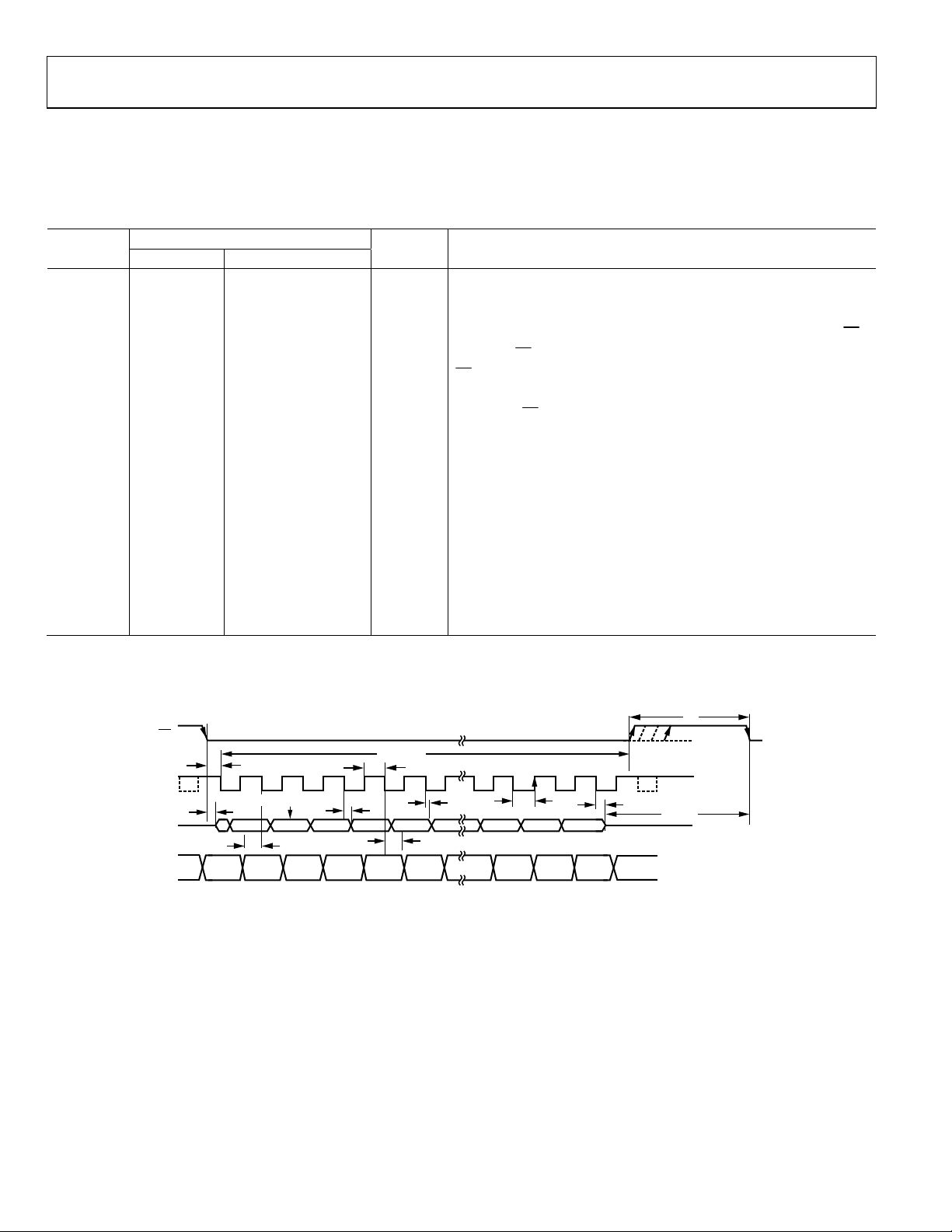
Figure 2. Serial Interface Timing Diagram
DON’T
CARE
SCLK
DOUT
DIN
THREE-
STATE
t
2
1 2 3 4 5 13 14 15 16
IDENTIFICATION BIT
t
3
ZERO
ZERO
WRITE ZERO
ADD0 SIGN DB11 DB10 DB2 DB1 DB0
t
9
REG
SEL
= 2.7 V to 5.25, V
DRIVE
) and timed from a voltage level of 1.6 V.
DRIVE
t
8
t
QUIET
THREE-STATE
≤ VCC,
DRIVE
t
1
04863-002
Rev. A | Page 6 of 36
AD7322
ABSOLUTE MAXIMUM RATINGS
TA = 25°C, unless otherwise noted
Table 4.
Parameter Rating
VDD to AGND, DGND −0.3 V to +16.5 V
VSS to AGND, DGND +0.3 V to −16.5 V
VDD to VCC V
− 0.3 V to 16.5 V
CC
VCC to AGND, DGND −0.3 V to +7 V
V
to AGND, DGND −0.3 V to +7 V
DRIVE
AGND to DGND −0.3 V to +0.3 V
Analog Input Voltage to AGND1 V
− 0.3 V to VDD + 0.3 V
SS
Stresses above those listed under Absolute Maximum Ratings
may cause permanent damage to the device. This is a stress
rating only; functional operation of the device at these or any
other conditions above those indicated in the operational
section of this specification is not implied. Exposure to absolute
maximum rating conditions for extended periods may affect
device reliability.
ESD CAUTION
Digital Input Voltage to DGND −0.3 V to +7 V
Digital Output Voltage to GND −0.3 V to V
DRIVE
+ 0.3 V
REFIN to AGND −0.3 V to VCC + 0.3 V
Input Current to Any Pin
Except Supplies
2
Operating Temperature Range −40°C to +85°C
Storage Temperature Range −65°C to +150°C
±10 mA
Junction Temperature 150°C
TSSOP Package
θJA Thermal Impedance 113.5°C/W
θJC Thermal Impedance 30°C/W
Pb-Free Temperature, Soldering
Reflow 260(0)°C
ESD 2.5 kV
1
If the analog inputs are driven from alternative VDD and VSS supply circuitry,
Schottky diodes should be placed in series with the AD7322’s VDD and VSS
supplies. See the Power Supply Configuration section.
2
Transient currents of up to 100 mA do not cause SCR latch-up.
Rev. A | Page 7 of 36
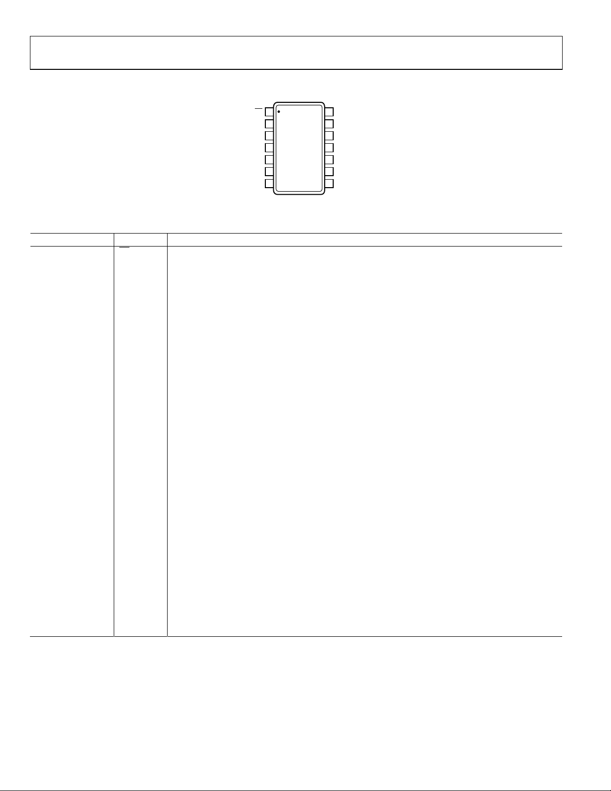
AD7322
PIN CONFIGURATION AND FUNCTION DESCRIPTIONS
CS
DIN
DGND
AGND
REFIN/OUT
V
V
IN
SS
0
1
2
3
AD7322
TOP VIE W
4
(Not to Scale)
5
6
7
14
13
12
11
10
9
8
SCLK
DGND
DOUT
V
DRIVE
V
CC
V
DD
VIN1
04863-003
Figure 3. Pin Configuration
Table 5. Pin Function Descriptions
Pin No. Mnemonic Description
1
CS
Chip Select. Active low logic input. This input provides the dual function of initiating conversions on
the AD7322 and framing the serial data transfer.
2 DIN
Data Input. Data to be written to the on-chip registers is provided on this input and is clocked into the
register on the falling edge of SCLK (see the Registers section).
3, 13 DGND
Digital Ground. Ground reference point for all digital circuitry on the AD7322. The DGND and AGND
voltages ideally should be at the same potential and must not be more than 0.3 V apart, even on a
transient basis.
4 AGND
Analog Ground. Ground reference point for all analog circuitry on the AD7322. All analog input signals
and any external reference signal should be referred to this AGND voltage. The AGND and DGND
voltages ideally should be at the same potential and must not be more than 0.3 V apart, even on a
transient basis.
5 REFIN/OUT
Reference Input/Reference Output. The on-chip reference is available on this pin for use external to the
AD7322. The nominal internal reference voltage is 2.5 V, which appears at the pin. A 680 nF capacitor
should be placed on the reference pin (see the Reference section). Alternatively, the internal reference
can be disabled and an external reference applied to this input. On power-up, the external reference
mode is the default condition.
6 VSS Negative Power Supply Voltage. This is the negative supply voltage for the analog input section.
7, 8 VIN0, VIN1
Analog Input 0 and Analog Input 1. The analog inputs are multiplexed into the on-chip track-and-hold.
The analog input channel for conversion is selected by programming the ADD0 channel address bit in
the control register. The inputs can be configured as single-ended, true differential, or pseudo differential
(see Tab le 10). The configuration of the analog inputs is selected by programming the mode bits,
Bit Mode 1 and Bit Mode 0, in the control register. The input range on each input channel is controlled by
programming the range register. Input ranges of ±10 V, ±5 V, ±2.5 V, and 0 V to +10 V can be selected
on each analog input channel when a +2.5 V reference voltage is used (see the Registers section).
9 VDD Positive Power Supply Voltage. This is the positive supply voltage for the analog input section.
10 VCC
Analog Supply Voltage, 2.7 V to 5.25 V. This is the supply voltage for the ADC core on the AD7322.
This supply should be decoupled to AGND.
11 V
DRIVE
Logic Power Supply Input. The voltage supplied at this pin determines at what voltage the interface
operates. This pin should be decoupled to DGND. The voltage at this pin may be different from that at
, but it should not exceed VCC by more than 0.3 V.
V
CC
12 DOUT
Serial Data Output. The conversion output data is supplied to this pin as a serial data stream. The bits
are clocked out on the falling edge of the SCLK input, and 16 SCLKs are required to access the data. The
data stream consists of two leading zero bits, a channel identification bit, the sign bit, and 12 bits of
conversion data. The data is provided MSB first (see the Serial Interface section).
14 SCLK
Serial Clock, Logic Input. A serial clock input provides the SCLK used for accessing the data from the
AD7322. This clock is also used as the clock source for the conversion process.
Rev. A | Page 8 of 36
AD7322
TYPICAL PERFORMANCE CHARACTERISTICS
1.0
VCC=V
0.8
0.6
0.4
0.2
0
–0.2
INL ERROR (LSB)
–0.4
–0.6
–0.8
–1.0
DRIVE
T
= 25°C
A
V
=±15V
DD,VSS
0 8192
1024 2048 3072 4096 5120 6144 7168
512 1536 2560 3584 4608 5632 6656 7680
INT/EXT 2.5V REFERENCE
=5V
±10V RANGE
+INL = +0.55LSB
–INL = –0.68LSB
CODE
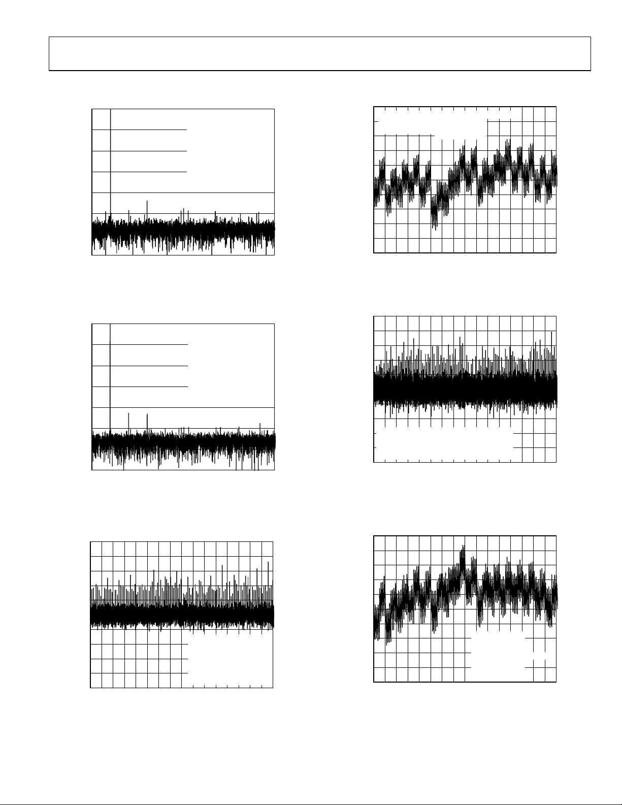
Figure 7. Typical INL True Differential Mode
04863-007
SNR (dB)
–20
–40
–60
–80
–100
–120
–140
0
0
50 100 150 200 250 300 350 400 450
FREQUENCY (kHz)
4096 POINT FFT
= V
V
CC
, VSS = ±15V
V
DD
T
= 25°C
A
INT/EXT 2.5V REFERENCE
±10V RANGE
f
= 50kHz
IN
SNR = 77.30dB
SINAD = 76.85dB
THD = –86.96d B
SFDR = –88.22d B
Figure 4. FFT True Differential Mode
DRIVE
= 5V
500
04863-004
SNR (dB)
–20
–40
–60
–80
–100
–120
–140
0
0
50 100 150 200 250 300 350 400 450
FREQUENCY (kHz)
4096 POINT FFT
= V
V
CC
V
DD
= 25°C
T
A
INT/EXT 2.5V REFERENCE
±10V RANGE
f
= 50kHz
IN
SNR = 74.67dB
SINAD = 74.03dB
THD = –82.68dB
SFDR = –85.40d B
= 5V
DRIVE
, VSS = ±15V
Figure 5. FFT Single-Ended Mode Figure 8. Typical DNL Single-Ended Mode
1.0
0.8
0.6
0.4
0.2
0
–0.2
DNL ERROR (LSB)
–0.4
–0.6
–0.8
–1.0
0 8192
1024 2048 3072 4096 5120 6144 7168
512 1536 2560 3584 4608 5632 6656 7680
VCC=V
DRIVE
T
=25°C
A
V
=±15V
DD,VSS
INT/EXT 2.5V REFERENCE
±10V RANGE
+DNL = +0.72LSB
–DNL = –0.22LSB
CODE
=5V
Figure 6. Typical DNL True Differential Mode
500
1.0
0.8
0.6
0.4
0.2
0
–0.2
DNL ERROR (LSB)
–0.4
VCC=V
–0.6
T
A
V
–0.8
DD,VSS
INT/EXT 2.5V REFERE NCE
–1.0
0 8192
512 1536 2560 3584 4608 5632 6656 7680
04863-005
1.0
0.8
0.6
0.4
0.2
0
–0.2
INL ERROR (LSB)
–0.4
–0.6
–0.8
–1.0
0 8192
512 1536 2560 3584 4608 5632 6656 7680
04863-006
=5V
DRIVE
= 25°C
= ±15V
1024 2048 3072 4096 5120 6144 7168
1024 2048 3072 4096 5120 6144 7168
±10V RANGE
+DNL = +0.79LSB
–DNL = –0.38LSB
CODE
VCC=V
DRIVE
T
= 25°C
A
V
=±15V
DD,VSS
INT/EXT 2.5V REFERENCE
±10V RANGE
+INL = + 0.87LSB
–INL = –0.49LSB
CODE
=5V
04863-043
04863-044
Figure 9. Typical INL Single-Ended Mode
Rev. A | Page 9 of 36
AD7322
–50
VCC=5V
= ±12V
V
–55
DD/VSS
= 25°C
T
A
f
=1MSPS
–60
THD (dB)
–100
–65
–70
–75
–80
–85
–90
–95
S
0V TO +10V SE
±10V DIFF
10
ANALOG INPUT FREQUENCY (kHz)
100
±10V SE
0V TO +10V DIFF
±5V SE
±5V DIFF
±2.5V DIFF
±2.5V SE
1000
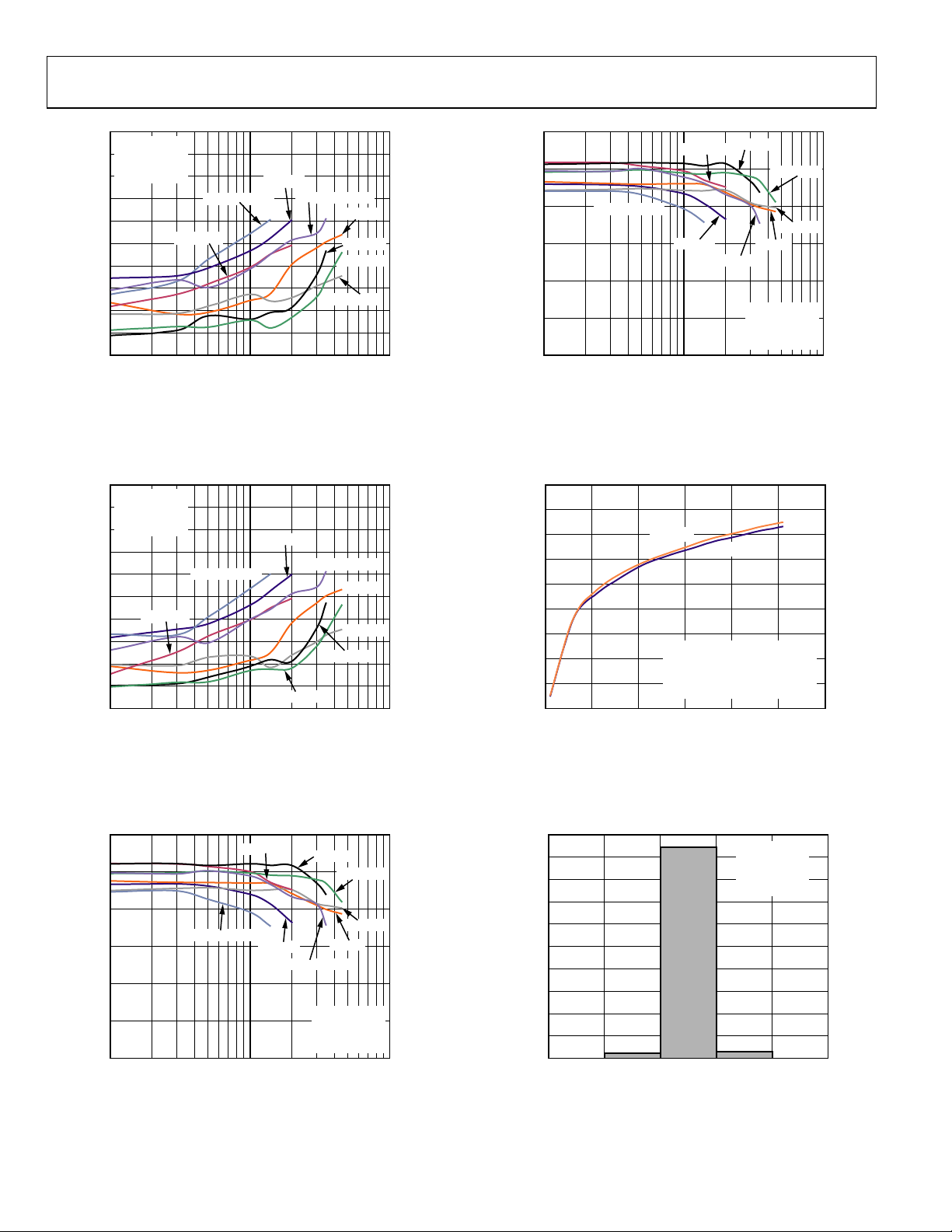
Figure 10. THD vs. Analog Input Frequency for Single-Ended (SE) and True
Differential Mode (Diff) at 5 V V
CC
04863-008
80
±10V DIFF
75
70
65
SINAD (dB)
60
55
50
10
0V TO + 10V SE
±10V SE
100
ANALOG INPUT F REQUENCY (kHz)
±5V DIFF
0V TO +10V DIFF
VCC=3V
V
T
f
S
±2.5V DIFF
±5V SE
DD/VSS
= 25°C
A
=1MSPS
±2.5V SE
= ±12V
1000
Figure 13. SINAD vs. Analog Input Frequency for Single-Ended (SE) and
Differential Mode (Diff) at 3 V V
CC
04863-011
–50
VCC=3V
= ±12V
V
–55
DD/VSS
T
= 25°C
A
=1MSPS
f
–60
THD (dB)
–100
–65
–70
–75
–80
–85
–90
–95
S
0V TO +10V SE
±10V DIFF
10
ANALOG INPUT F REQUENCY (kHz)
100
±10V SE
0V TO +10V DIFF
±5V SE
±2.5V SE
±5V DIFF
±2.5V DIFF
1000
Figure 11. THD vs. Analog Input Frequency for Single-Ended (SE) and True
Differential Mode (Diff) at 3 V V
80
75
70
65
SINAD (dB)
60
55
50
10
0V TO + 10V SE
ANALOG INPUT F REQUENCY (kHz)
±10V DIFF
±10V SE
100
CC
±5V DIFF
±2.5V DIFF
±5V SE
0V TO + 10V DIFF
VCC=5V
V
DD/VSS
= 25°C
T
A
=1MSPS
f
S
±2.5V SE
= ±12V
1000
Figure 12. SINAD vs. Analog Input Frequency for Single-Ended (SE) and
Differential Mode (Diff) at 5 V V
CC
–50
–55
–60
–65
–70
–75
–80
–85
–90
CHANNEL-TO- CHANNEL ISO LATION (dB)
–95
0
100 200 300 400 500
04863-009
FREQUENCY O F INPUT NO ISE (kHz)
VCC=3V
VDD/VSS=±12V
SINGLE-E NDED MODE
f
S
T
A
50kHz ON SELECT ED CHANNE L
=1MSPS
= 25°C
VCC=5V
600
04863-012
Figure 14. Channel-to-Channel Isolation
10k
9k
8k
7k
6k
5k
4k
3k
NUMBER OF OCCURRENCES
2k
1k
0
0
–2
04863-010
228
–1 0 1 2
9469
CODE
VCC=5V
= ±12V
V
DD/VSS
RANGE = ± 10V
10k SAMPLES
= 25°C
T
A
303
0
04863-013
Figure 15. Histogram of Codes True Differential Mode
Rev. A | Page 10 of 36
AD7322
8k
7600
7k
6k
5k
4k
3k
2k
NUMBER OF OCCURRENCES
1201
1165
1k
023
0
–3
–2 –1 0 1 2 3
CODE
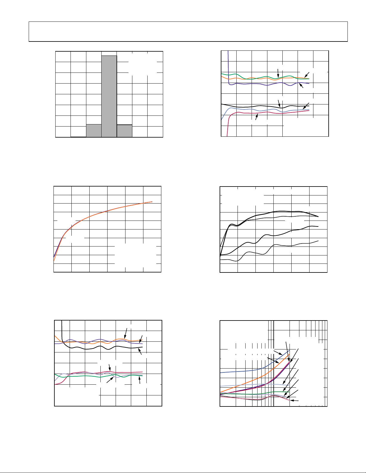
Figure 16. Histogram of Codes, Single-Ended Mode
–50
–55
–60
–65
VCC = 5V
–70
–75
CMRR (dB)
–80
–85
–90
–95
–100
0
= 3V
V
CC
DIFFERENTIAL MODE
f
= 50kHz
IN
V
DD/VSS
f
= 1MSPS
S
= 25°C
T
A
200 400 600 800 1000 1200
RIPPLE FREQUENCY (kHz)
Figure 17. CMRR vs. Common-Mode Ripple Frequency
VCC = 5V
= ±12V
V
DD/VSS
RANGE = ±10V
10k SAMPLES
= 25°C
T
A
11 0
= ±12V
04863-014
04863-055
2.0
1.5
1.0
INL = 500kSPS
INL = 750kSPS
0.5
0
–0.5
INL ERROR (LSB)
INL = 500kSPS
INL = 1MSPS
INL = 750kSPS
–1.0
–1.5
–2.0
5 7 9 11 13 15 17 19
INL = 1MSPS
±V
DD/VSS
SUPPLY VOLTAGE (V)
±5V RANGE
V
CC=VDRIVE
INTERNAL REFERENCE
SINGLE- ENDED MODE
=5V
04863-050
Figure 19. INL Error vs. Supply Voltage at 500 kSPS, 750 kSPS, and 1 MSPS
–50
100mV p-p SI NE WAVE ON EACH SUPPLY
–55
NO DECOUPLING
SINGLE-E NDED MODE
f
=1MSPS
S
–60
–65
–70
VCC=3V
VCC=5V
–75
PSRR (dB)
–80
–85
VDD=12V
VSS=–12V
–90
–95
–100
0 1200
200 400 600 800 1000
SUPPLY RIPPLE FREQUENCY (kHz)
Figure 20. PSRR vs. Supply Ripple Frequency Without Supply Decoupling
04863-054
2.0
1.5
DNL = 750kSPS
DNL = 500kS PS
1.0
0.5
±V
DD/VSS
DNL = 1MSP S
DNL = 750kS PS
SUPPLY VOLTAGE (V)
0
–0.5
DNL ERROR (LSB)
–1.0
±5V RANGE
V
CC=VDRIVE
–1.5
INTERNAL RE FERENCE
SINGLE-ENDED MODE
–2.0
5 7 9 11 13 15 17 19
=5V
DNL = 1MSP S
DNL = 500kSPS
04863-049
Figure 18. DNL Error vs. Supply Voltage at 500 kSPS, 750 kSPS, and 1 MSPS
Rev. A | Page 11 of 36
–50
VCC=V
V
DD/VSS
–55
T
=25°C
A
INTERNAL REFERENCE
–60
RANGE = ± 10V AND ±2.5V
–65
R
IN
–70
–75
THD (dB)
–80
–85
–90
–95
10
=5V
DRIVE
= ±12V
= 2000Ω, ±10V RANGE
R
IN
= 1000Ω, ±10V RANGE
ANALOG INPUT FREQUENCY (kHz)
RIN= 100Ω, ±10V RANGE
R
IN
±10V RANGE
R
IN
±2.5V RANGE
R
IN
±2.5V RANGE
R
IN
±2.5V RANGE
R
IN
±2.5V RANGE
R
IN
±2.5V RANGE
100
=50Ω,
=4700Ω,
=2000Ω,
=1000Ω,
=100Ω,
=50Ω,
1000
04863-015
Figure 21. THD vs. Analog Input Frequency for Various Source Impedances,
True Differential Mode
 Loading...