Analog Devices AD7306JR, AD7306JN, AD7306AR, AD7306AN Datasheet

+5 V Powered
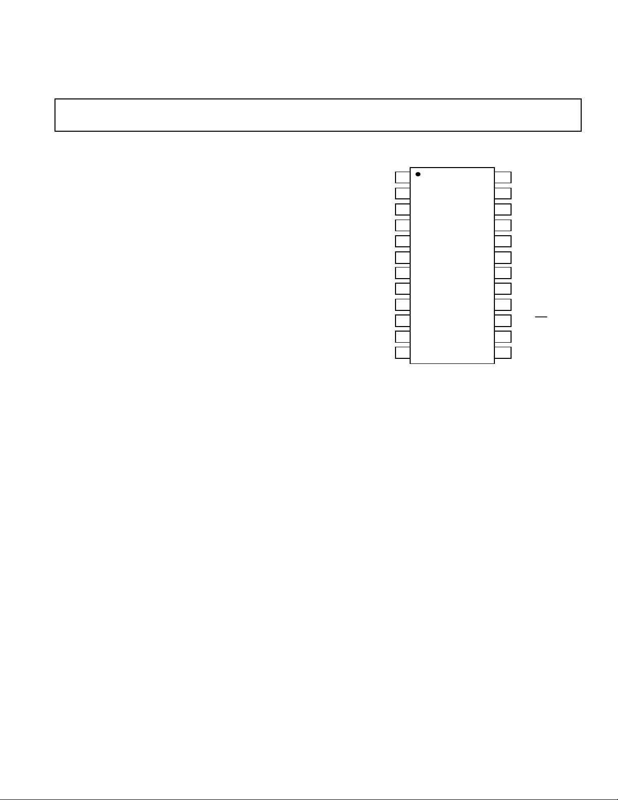
V+
C1+
C1–
V–
C2–
C2+
GND
NC
NC
NC = NO CONNECT
1
2
3
4
5
6
7
8
9
10
11
12
24
23
22
21
16
15
14
13
20
19
18
17
AD7306
SOIC
TOP VIEW
(Not to Scale)
GND
R1
IN
/R1IN(A)
T2
OUT
T1
OUT
R2
IN
R1IN(B)
T3
OUT
(B)
R2
OUT
T3
IN
232/422 SEL
V
CC
R1
OUT
T1
IN
T2
IN
T3
OUT
(A)
a
FEATURES
RS-232 and RS-422 on One Chip
Single +5 V Supply
0.1 mF Capacitors
Short Circuit Protection
Excellent Noise Immunity
Low Power BiCMOS Technology
High Speed, Low Skew RS-422 Operation
–408C to +858C Operations
APPLICATIONS
DTE-DCE Interface
Packet Switching
Local Area Networks
Data Concentration
Data Multiplexers
Integrated Services Digital Network (ISDN)
GENERAL DESCRIPTION
The AD7306 line driver/receiver is a 5 V monolithic product
which provides an interface between TTL signal levels and dual
standard EIA RS-232/RS-422 signal levels. The part contains
two RS-232 drivers, one RS-422 driver, one RS-232 receiver,
and one receiver path which can be configured either as RS-232
or as RS-422.
An internal charge pump voltage converter facilitates operation
from a single +5 V power supply. The internal charge pump
generates ±10 V levels allowing RS-232 output levels to be developed without the need for external bipolar power supplies.
A highly efficient charge pump design allows operation using
non polarized, miniature 0.1 µF capacitors. This gives a consid-
erable saving in printed circuit board space over conventional
products which can use up to 10 µF capacitors. The charge
pump output voltages may also be used to power external circuitry which requires dual supplies.
RS-232/RS-422 Transceiver
AD7306
FUNCTIONAL BLOCK DIAGRAM
The RS-232 channels are suitable for communications rates up
to 100 kHz and the RS-422 channels are suitable for high speed
communications up to 5 MHz. The RS-422 transmitter complementary outputs are closely matched and feature low timing
skew between the complementary outputs. This is often an essential requirement to meet tight system timing specifications.
All inputs feature ESD protection, all driver outputs feature
high source and sink current capability and are internally protected against short circuits on the outputs. An epitaxial layer is
used to guard against latch-up.
The part is available in a 24-lead SOIC and 24-pin plastic DIP
package.
REV. B
Information furnished by Analog Devices is believed to be accurate and
reliable. However, no responsibility is assumed by Analog Devices for its
use, nor for any infringements of patents or other rights of third parties
which may result from its use. No license is granted by implication or
otherwise under any patent or patent rights of Analog Devices.
One Technology Way, P.O. Box 9106, Norwood, MA 02062-9106, U.S.A.
Tel: 617/329-4700 Fax: 617/326-8703

AD7306–SPECIFICA TIONS
(VCC = +5 V 6 5%, C1 = C2 = C3 = C4 = 0.1 mF. All specifications T
T
unless otherwise noted.)
MAX
MIN
to
Parameter Min Typ Max Units Test Conditions/Comments
RS-232 DRIVER
TTL Input Logic Low, V
TTL Input Logic High, V
INL
INH
2.0 V
Input Logic Current 0.1 ±10 µAV
0.8 V
= 0 V to V
IN
CC
RS-232 High Level Output Voltage 5.0 7.3 V RL = 3 kΩ
RS-232 Low Level Output Voltage –5.0 –6.5 V R
Output Short Circuit Current ±5 ±12 mA V
Slew Rate 8 20 30 V/µsC
4V/µsC
Output Resistance (Powered Down) 300 10M Ω VCC = 0 V, V
= 3 kΩ
L
= 0 V, TA = 0°C to +70°C
OUT
= 50 pF, RL = 3 kΩ
L
= 2500 pF, RL = 3 kΩ
L
OUT
= ±3 V
RS-232 RECEIVER
Input Voltage Range –15 +15 V
RS-232 Input Threshold Low 0.8 1.3 V
RS-232 Input Threshold High 1.7 2.4 V
RS-232 Input Hysteresis 0.1 0.4 1.0 V
RS-232 Input Resistance 3 5 7 kΩ
TTL Output Voltage Low, V
TTL Output Voltage High, V
OL
OH
3.5 4.8 V I
0.2 0.4 V I
= +4 mA
OUT
= –4 mA
OUT
RS-422 DRIVER
TTL Input Logic Low, V
TTL Input Logic High, V
INL
INH
2.0 V
Logic Input Current 0.1 ±10 µAV
0.8 V
= 0 V to V
IN
CC
Differential Output Voltage 5.0 V VCC = 5 V, RL Diff = ∞; Figure 3
2VR
Diff = 100 Ω; Figure 3
L
Common-Mode Output Voltage 3 V
∆|V
Output Short Circuit Current 35 150 mA 0 V ≤ V
| for Complementary O/P States 0.2 V RL Diff = 100 Ω
OUT
CMR
≤ +7 V
RS-422 RECEIVER
Common-Mode Voltage Range ± 7 V Typical RS-422 Input Voltage <5 V
Differential Input Threshold Voltage –0.2 +0.2 V
Input Voltage Hysteresis 70 mV V
CM
= 0 V
Input Resistance 3 5 7 kΩ
TTL Output Voltage Low, V
TTL Output Voltage High, V
232/
422 SEL Input
Input Logic Low, V
Input Logic High, V
INL
INH
OL
OH
3.5 4.8 V I
2.0 V
Logic Input Current 0.1 ±10 µAV
0.2 0.4 V I
0.8 V
= +4.0 mA
OUT
= –4.0 mA
OUT
= 0 V to V
IN
CC
POWER SUPPLY CURRENT
I
CC
10 15 mA Outputs Unloaded
CHARGE PUMP VOLTAGE GENERATOR
V+ Output Voltage 9 V RS-232 Output Unloaded;
See Typical Performance Curves
V– Output Voltage –9 V RS-232 Outputs Unloaded;
See Typical Performance Curves
Generator Rise Time 200 µs
Specifications subject to change without notice.
–2–
REV. B

AD7306
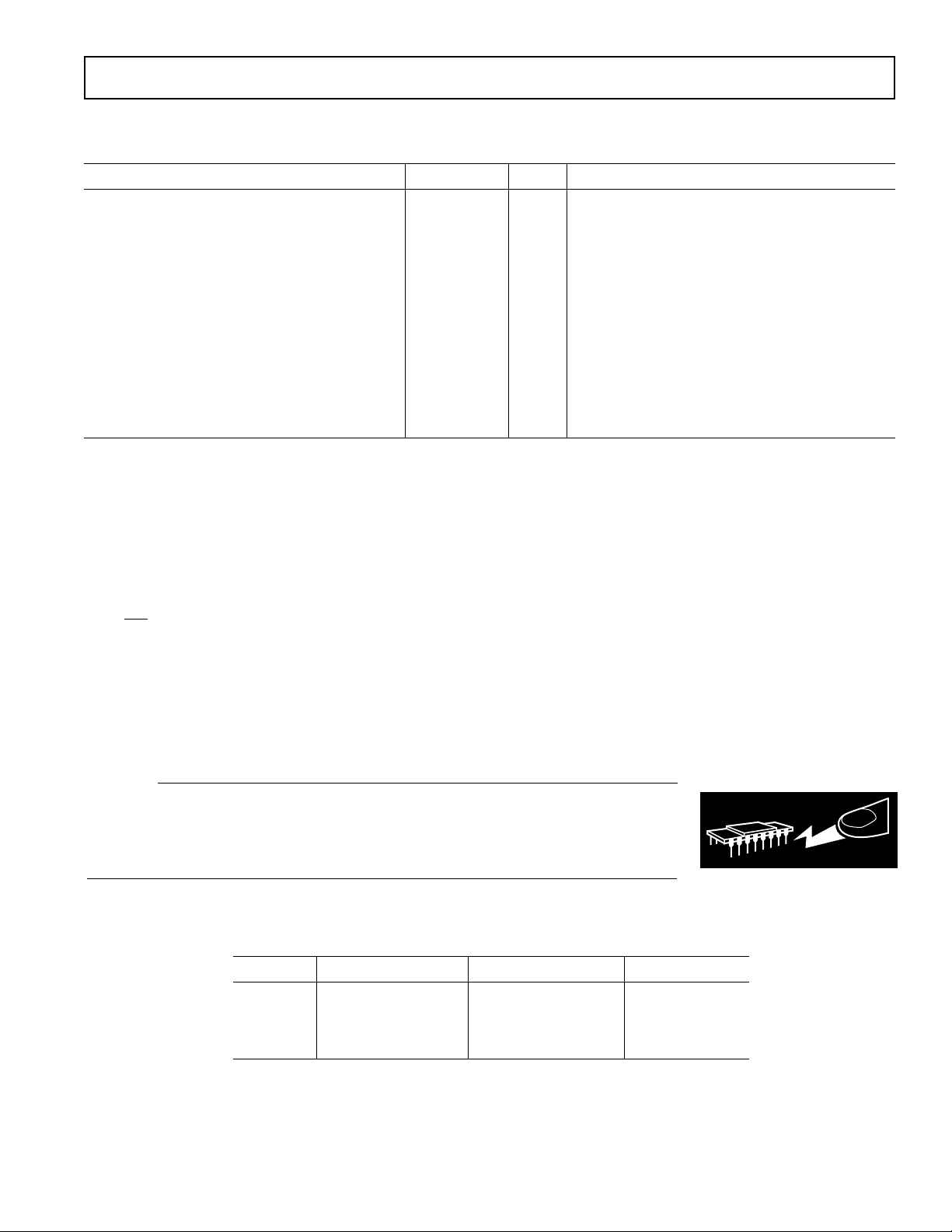
WARNING!
ESD SENSITIVE DEVICE
TIMING SPECIFICATIONS
(VCC = +5 V 6 5%, C1 = C2 = C3 = C4 = 0.1 mF. All specifications T
unless otherwise noted.)
MIN
to T
MAX
Parameter Typ Max Units Test Conditions/Comments
RS-422 Driver
Propagation Delay Input to Output T
RS-422 O/P to O/P T
Driver Rise/Fall Time T
SKEW
R
, T
F
PLH
, T
PHL
35 100 ns RL Diff = 100 Ω. CL1 = CL2 = 100 pF, Figures 2 & 4
210nsR
Diff = 100 Ω. CL1 = CL2 = 100 pF, Figures 2 & 4
L
15 40 ns RL Diff = 100 Ω. CL1 = CL2 = 100 pF, Figures 2 & 4
RS-422 Receiver
Propagation Delay Input to Output T
PLH
, T
PHL
70 200 ns CL = 15 pF. Figure 5
RS-232/RS-422 Enable
RS-232 Disable to RS-422 Enable T
RS-422 Disable to RS-232 Enable T
EN1
EN2
70 200 ns Figure 6
70 200 ns Figure 6
Transmission Rate (RS-422) 5 MHz
RS-232 Receiver
Propagation Delay Input to Output 1000 ns
Transmission Rate (RS-232) 100 kHz C
= 50 pF
L
20 kHz CL = 2.5 nF
ABSOLUTE MAXIMUM RATINGS*
(TA = +25°C unless otherwise noted)
VCC . . . . . . . . . . . . . . . . . . . . . . . . . . . . . . . . . . . . . . . . . +7 V
V+ . . . . . . . . . . . . . . . . . . . . . . . . . . .(V
–0.3 V) to +13.2 V
CC
V– . . . . . . . . . . . . . . . . . . . . . . . . . . . . . . . .+0.3 V to –13.2 V
Inputs
T1
, T2IN . . . . . . . . . . . . . . . . . . . . . . . . . . . . . . .V– to V+
IN
T3
. . . . . . . . . . . . . . . . . . . . . . . . . . . . . . . .–0.3 V to V+
IN
R1
A/B, R2IN . . . . . . . . . . . . . . . . . . . . . . .–25 V to +25 V
IN
232/
422 SEL . . . . . . . . . . . . . . . . . . . . . . . . . .–0.3 V to V+
Outputs
T1
, T2
OUT
T3
(A), (B) . . . . . . . . . . . . . . . . . . . . . . . –0.3 V to +7 V
OUT
R1
, R2
OUT
. . . . . . . . . . . . . . . . . . . . . . .–15 V to +15 V
OUT
. . . . . . . . . . . . . . . . –0.3 V to (VCC + 0.3 V)
OUT
Short Circuit Duration
T
. . . . . . . . . . . . . . . . . . . . . . . . . . . . . . . . .Continuous
OUT
Power Dissipation
Small Outline . . . . . . . . . . . . . . . . . . . . . . . . . . . . . 650 mW
DIP . . . . . . . . . . . . . . . . . . . . . . . . . . . . . . . . . . . . 650 mW
Operating Temperature Range
Commercial (J Version) . . . . . . . . . . . . . . . . . 0°C to +70°C
Industrial (A Version) . . . . . . . . . . . . . . . . –40°C to +85°C
Storage Temperature Range . . . . . . . . . . . . –65°C to +150°C
Lead Temperature (Soldering, 10 secs) . . . . . . . . . . . +300°C
*Stresses above those listed under “Absolute Maximum Ratings” may cause
permanent damage to the device. This is a stress rating only and functional
operation of the device at these or any other conditions above those listed in the
operational sections of this specification is not implied. Exposure to absolute
maximum ratings for extended periods of time may affect device reliability.
CAUTION
ESD (electrostatic discharge) sensitive device. Electrostatic charges as high as 4000 V readily
accumulate on the human body and test equipment and can discharge without detection.
Although the AD7306 features proprietary ESD protection circuitry, permanent damage may
occur on devices subjected to high energy electrostatic discharges. Therefore, proper ESD
precautions are recommended to avoid performance degradation or loss of functionality.
REV. B
ORDERING GUIDE
Model Temperature Range Package Description Package Option
AD7306JR 0°C to +70°C 24-Lead SOIC R-24
AD7306JN 0°C to +70°C 24-Pin DIP N-24
AD7306AR –40°C to +85°C 24-Lead SOIC R-24
AD7306AN –40°C to +85°C 24-Pin DIP N-24
–3–
 Loading...