

Picoampere Input Current
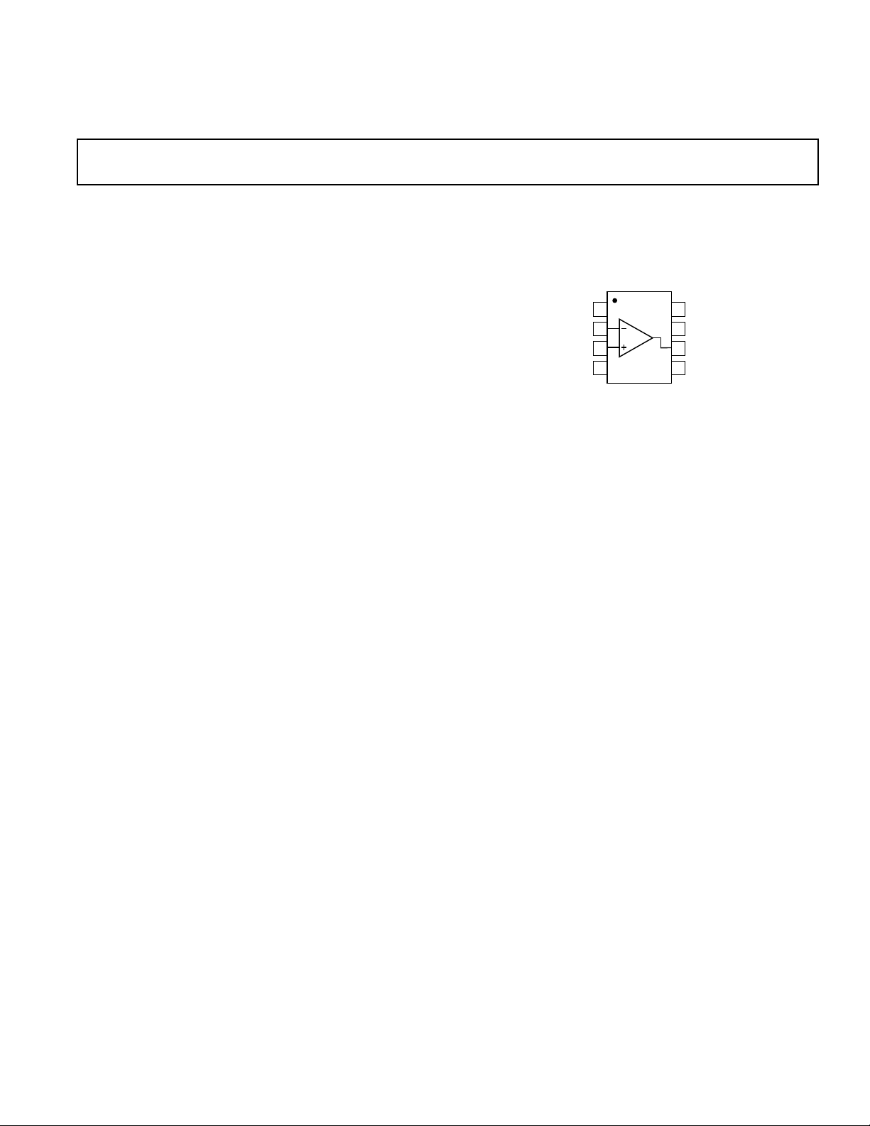
OFFSET
NULL
–IN
+IN
V–
OFFSET
NULL
V+
OUTPUT
OVER
COMP
1
2
3
4
8
7
6
5
TOP VIEW
AD705
a
FEATURES
DC PERFORMANCE
25 mV max Offset Voltage (AD705T)
0.6 mV/8C max Drift (AD705K/T)
100 pA max Input Bias Current (AD705K)
600 pA max I
114 dB min CMRR (AD705K/T)
114 dB min PSRR (AD705T)
200 V/mV min Open Loop Gain
0.5 mV p-p typ Noise, 0.1 Hz to 10 Hz
600 mA max Supply Current
AC PERFORMANCE
0.15 V/µs Slew Rate
800 kHz Unity Gain Crossover Frequency
10,000 pF Capacitive Load Drive Capability
Low Cost
Available in 8-Pin Plastic Mini-DlP, Hermetic Cerdip
and Surface Mount (SOIC) Packages
MIL-STD-883B Processing Available
Dual Version Available: AD706
Quad Version: AD704
APPLICATIONS
Low Frequency Active Filters
Precision Instrumentation
Precision Integrators
PRODUCT DESCRIPTION
The AD705 is a low power bipolar op amp that has the low input bias current of a BiFET amplifier but which offers a significantly lower I
of the advantages of BiFET and bipolar op amps without their
inherent disadvantages. It utilizes superbeta bipolar input transistors to achieve the picoampere input bias current levels of
FET input amplifiers (at room temperature), while its I
cally only increases 5 times vs. BiFET amplifiers which exhibit a
1000X increase over temperature. This means that, at room
temperature, while a typical BiFET may have less I
AD705, the BiFET’s input current will increase to a level of
several nA at +125°C. Superbeta bipolar technology also permits the AD705 to achieve the microvolt offset voltage and low
noise characteristics of a precision bipolar input amplifier.
The AD705 is a high quality replacement for the industrystandard OP07 amplifier while drawing only one sixth of its
power supply current. Since it has only 1/20th the input bias
current of an OP07, the AD705 can be used with much higher
source impedances, while providing the same level of dc precision. In addition, since the input bias currents are at picoAmp
Over MIL Temperature Range (AD705T)
B
drift over temperature. The AD705 offers many
B
typi-
B
than the
B
Bipolar Op Amp
AD705
CONNECTION DIAGRAM
Plastic Mini-DIP (N)
Cerdip (Q) and
Plastic SOIC (R) Packages
levels, the commonly used “balancing” resistor (connected between the noninverting input of a bipolar op amp and ground) is
not required.
The AD705 is an excellent choice for use in low frequency active filters in 12- and 14-bit data acquisition systems, in precision instrumentation and as a high quality integrator.
The AD705 is internally compensated for unity gain and is
available in five performance grades. The AD705J and AD705K
are rated over the commercial temperature range of 0°C to
+70°C. The AD705A and AD705B are rated over the industrial
temperature range of –40°C to +85°C. The AD705T is rated
over the military temperature range of –55°C to +125°C and is
available processed to MIL-STD-883B, Rev. C.
The AD705 is offered in three varieties of 8-pin package: plastic
DIP, hermetic cerdip and surface mount (SOIC). “J” grade
chips are also available.
PRODUCT HIGHLIGHTS
1. The AD705 is a low drift op amp that offers BiFET level
input bias currents, yet has the low I
fier. It upgrades the performance of circuits using op amps
such as the LT1012.
2. The combination of Analog Devices’ advanced superbeta
processing technology and factory trimming provides both
low drift and high dc precision.
3. The AD705 can be used in applications where a chopper amplifier would normally be required but without the chopper’s
inherent noise and other problems.
drift of a bipolar ampli-
B
REV. B
Information furnished by Analog Devices is believed to be accurate and
reliable. However, no responsibility is assumed by Analog Devices for its
use, nor for any infringements of patents or other rights of third parties
which may result from its use. No license is granted by implication or
otherwise under any patent or patent rights of Analog Devices.
One Technology Way, P.O. Box 9106, Norwood, MA 02062-9106, U.S.A.
Tel: 617/329-4700 Fax: 617/326-8703

AD705–SPECIFICATIONS
(@ TA = +258C, VCM = 0 V, and VS = 615 V dc, unless otherwise noted)
Parameter Conditions Min Typ Max Min Typ Max Min Typ Max Units
AD705J/A AD705K/B AD705T
INPUT OFFSET VOLTAGE
Initial Offset 30 90 10 35 10 25 µV
Offset T
vs. Temp, Average TC 0.2 1.2 0.2 0.6 0.2 0.6 µV/°C
MIN
to T
MAX
45 150 25 60 25 60 µV
vs. Supply (PSRR) VS = ±2 V to ±18 V 110 129 110 129 114 129 dB
T
to T
MIN
Long Term Stability 0.3 0.3 0.3 µV/month
INPUT BIAS CURRENT
MAX
1
VS = ±2.5 V to ±18 V 108 126 108 126 108 126 dB
VCM = 0 V 60 150 30 100 30 100 pA
VCM = ±13.5 V 80 200 50 150 50 150 pA
vs. Temp, Average TC 0.3 0.3 0.6 pA/°C
T
MIN
T
MIN
to T
to T
MAX
MAX
VCM = 0 V 80 250 50 150 90 600 pA
VCM = ± 13.5 V 100 450 70 350 120 750 pA
INPUT OFFSET CURRENT VCM = 0 V 40 150 30 100 30 100 pA
VCM = ±13.5 V 40 200 30 150 30 150 pA
vs. Temp, Average TC 0.3 0.3 0.4 pA/°C
T
to T
MIN
MIN
to T
MAX
MAX
T
VCM = 0 V 80 250 50 150 80 250 pA
VCM = ±13.5 V 80 450 50 350 80 450 pA
FREQUENCY RESPONSE
Unity Gain
Crossover Frequency 0.4 0.8 0.4 0.8 0.4 0.8 MHz
Slew Rate, Unity Gain G = –1 0.1 0.15 0.1 0.15 0.1 0.15 V/µs
Slew Rate T
MIN
to T
MAX
0.05 0.15 0.05 0.15 0.05 0.15 V/µs
INPUT IMPEDANCE
Differential 40i2 40i240i2MΩipF
Common Mode 300i2 300i2 300i2GΩipF
INPUT VOLTAGE RANGE
Common-Mode Voltage ± 13.5 ± 14 ±13.5 ± 14 ± 13.5 ± 14 V
COMMON-MODE
REJECTION RATIO VCM = ±13.5 V 110 132 114 132 114 132 dB
T
MIN
to T
MAX
108 128 108 128 108 128 dB
INPUT VOLTAGE NOISE 0.1 Hz to 10 Hz 0.5 0.5 1.0 0.5 1.0 µV p-p
f = 10 Hz 17 17 17 nV/√Hz
f = 1 kHz 15 22 15 22 15 22 nV/√Hz
INPUT CURRENT NOISE f = 10 Hz 50 50 50 fA/√Hz
OPEN-LOOP GAIN VO = ±12 V
R
= 10 kΩ 300 2000 400 2000 400 2000 V/mV
LOAD
T
to T
MIN
VO = ±10 V
R
T
MAX
= 2 kΩ 200 1000 300 1000 300 1000 V/mV
LOAD
to T
MIN
MAX
200 1500 300 1500 300 1500 V/mV
150 1000 200 1000 200 1000 V/mV
OUTPUT CHARACTERISTICS
Voltage Swing R
Current Short Circuit ±15 ± 15 ±15 mA
= 10 kΩ±13 ±14 ± 13 ±14 ±13 ±14 V
LOAD
T
MIN
to T
MAX
613 ±14 613 ±14 613 ±14 V
Capacitive Load
Drive Capability Gain = +1 10,000 10,000 10,000 pF
Output Resistance Open Loop 200 200 200 Ω
POWER SUPPLY
Rated Performance ±15 ± 15 ±15 V
Operating Range 62.0 618 62.0 618 62.0 618 V
Quiescent Current 380 600 380 600 380 600 µA
T
MIN
to T
MAX
400 800 400 800 400 800 µA
TEMPERATURE RANGE
FOR RATED PERFORMANCE
Commercial (0°C to +70°C) AD705J AD705K
Industrial (–40°C to +85°C) AD705A AD705B
Military (–55°C to +125°C) AD705T
–2–
REV. B
AD705
WARNING!
ESD SENSITIVE DEVICE
Parameter Conditions Min Typ Max Min Typ Max Min Typ Max Units
AD705J/A AD705K/B AD705T
PACKAGE OPTIONS
8-Pin Cerdip (Q-8) AD705AQ AD705BQ AD705TQ
8-Pin Plastic Mini-DIP (N-8) AD705JN AD705KN
8-Pin SOIC (R-8) AD705JR
Chips AD705JCHIPS
TRANSISTOR COUNT # of Transistors 45 45 45
NOTES
1
Bias current specifications are guaranteed maximum at either input.
All min and max specifications are guaranteed
Specifications in boldface are tested on all production units at final electrical test. Results from those tests are used to calculate outgoing quality levels.
Specifications subject to change without notice.
METALIZATION PHOTOGRAPH
Dimensions shown in inches and (mm).
NULL
8
0.074 (1.88)
8
+V
V
S
OUT
7
6
7
6
5 OVER COMP
5
ABSOLUTE MAXIMUM RATINGS
Supply Voltage . . . . . . . . . . . . . . . . . . . . . . . . . . . . . . . . ±18 V
Internal Power Dissipation
Input Voltage . . . . . . . . . . . . . . . . . . . . . . . . . . . . . . . . . . . ±V
Differential Input Voltage
2
. . . . . . . . . . . . . . . . . . . 650 mW
3
. . . . . . . . . . . . . . . . . . . . . ±0.7 V
Output Short Circuit Duration . . . . . . . . . . . . . . . . Indefinite
Storage Temperature Range (N, R) . . . . . . . –65°C to +125°C
Storage Temperature Range (Q) . . . . . . . . . –65°C to +150°C
Operating Temperature Range
1
AD705J/K . . . . . . . . . . . . . . . . . . . . . . . . . . . 0°C to +70°C
0.0677
(1.72)
NULL 1
–IN 2
1
2
3
3
+IN
4
4 –V
S
AD705A/B . . . . . . . . . . . . . . . . . . . . . . . . . –40°C to +85°C
AD705T . . . . . . . . . . . . . . . . . . . . . . . . . . –55°C to +125°C
Lead Temperature Range (Soldering 60 sec) . . . . . . . . +300°C
NOTES
1
Stresses above those listed under “Absolute Maximum Ratings” may cause
permanent damage to the device. This is a stress rating only and functional
operation of the device at these or any other conditions above those indicated in
the operational section of this specification is not implied. Exposure to absolute
maximum rating conditions for extended periods may affect device reliability.
2
Specification is for device in free air:
8-Pin Plastic Package: θJA = 165°C/Watt
8-Pin Cerdip Package: θJA = 110°C/Watt
8-Pin Small Outline Package: θJA = 155°C/Watt
3
The input pins of these amplifiers are protected by back-to-back diodes. If the
differential voltage exceeds ±0.7 V, external series protection resistors should be
added to limit the input current to less than 25 mA.
S
CAUTION
ESD (electrostatic discharge) sensitive device. Electrostatic charges as high as 4000 V readily
accumulate on the human body and test equipment and can discharge without detection.
Although the AD705 features proprietary ESD protection circuitry, permanent damage may
occur on devices subjected to high energy electrostatic discharges. Therefore, proper ESD
precautions are recommended to avoid performance degradation or loss of functionality.
REV. B
ORDERING GUIDE
Temperature Package Package
Model Range Description Option
AD705AQ –40°C to +85°C 8-Pin Ceramic DIP Q-8
AD705BQ –40°C to +85°C 8-Pin Ceramic DIP Q-8
AD705JCHIPS 0°C to +70°C Bare Die
AD705JN 0°C to +70°C 8-Pin Plastic DIP N-8
AD705JR 0°C to +70°C 8-Pin Plastic SOIC R-8
AD705JR-REEL 0°C to +70°C 8-Pin Plastic SOIC R-8
AD705JR-REEL7 0°C to +70°C 8-Pin Plastic SOIC R-8
AD705KN 0°C to +70°C 8-Pin Plastic DIP N-8
AD705TQ –55°C to +125° C 8-Pin Ceramic DIP Q-8
AD705TQ/883B –55°C to +125°C 8-Pin Ceramic DIP Q-8
–3–

AD705–Typical Characteristics
0
40
80
120
160
200
INPUT OFFSET CURRENT – Picoamperes
SAMPLE SIZE: 510
–120 –60 0 +60 +120
NUMBER OF UNITS
1k 10k 100k 1M 10M 100M
SOURCE RESISTANCE – Ω
SOURCE RESISTANCE
MAY BE EITHER BALANCED
OR UNBALANCED
100
10
1.0
0.1
OFFSET VOLTAGE DRIFT – µV/°C
60
40
20
0
–20
–40
–60
–15 –10 –5 0 +5 +10 +15
NEGATIVE I
B
POSITIVE I
B
COMMON MODE VOLTAGE – Volts
INPUT BIAS CURRENT – pA
(@ +258C, VS = 615 V, unless otherwise noted)
100
SAMPLE SIZE: 610
80
60
40
NUMBER OF UNITS
20
0
40–20–20+40+80– –60 +60 +80
INPUT OFFSET VOLTAGE – Microvolts
0
Figure 1. Typical Distribution of
Input Offset Voltage
+V
S
–0.5
–1.0
–1.5
+1.5
+1.0
+0.5
(REFERRED TO SUPPLY VOLTAGES)
–V
S
INPUT COMMON MODE VOLTAGE LIMIT – Volts
0 5 10 15 20
SUPPLY VOLTAGE – ±Volts
200
SAMPLE SIZE:
160
120
NUMBER OF UNITS
1040
80
40
0
–120
–60
INPUT BIAS CURRENT – Picoamperes
0
+60 +120
Figure 2. Typical Distribution of
Input Bias Current
35
30
25
20
15
10
OUTPUT VOLTAGE – Volts p-p
5
0
1k 10k 100k 1M
FREQUENCY – Hz
Figure 3. Typical Distribution of
Input Offset Current
Figure 4. Input Common-Mode
Voltage Range vs. Supply Voltage
50
SAMPLE SIZE: 85
–55°C TO +125°C
40
30
20
NUMBER OF UNITS
10
0
Figure 7. Typical Distribution of
Offset Voltage Drift
–0.4 –0.2 0 +0.2 +0.4
OFFSET VOLTAGE DRIFT – µV/°C
Figure 5. Large Signal Frequency
Response
4
3
2
1
CHANGE IN OFFSET VOLTAGE – µV
0
012 34 5
WARM-UP TIME IN MINUTES
Figure 8. Change in Input Offset
Voltage vs. Warm-Up Time
Figure 6. Offset Voltage Drift vs.
Source Resistance
Figure 9. Input Bias Current vs.
Common-Mode Voltage
–4–
REV. B

AD705
0.5µV
0510
TIME – Seconds
OUTPUT VOLTAGE LIMIT – Volts
(REFERRED TO SUPPLY VOLTAGES)
+V
S
–0.5
–1.0
–1.5
+1.5
+1.0
+0.5
–V
S
0 5 10 15 20
SUPPLY VOLTAGE – ±Volts
1000
Hz
√
100
10
VOLTAGE NOISE – nV/
1
1 10 100 1000
FREQUENCY – Hz
Figure 10. Input Noise Voltage
Spectral Density
500
450
400
350
QUIESCENT CURRENT – µA
300
0 5 10 15 20
+125°C
+25°C
+55°C
SUPPLY VOLTAGE – ±Volts
1000
Hz
√
100
10kΩ100Ω
10
CURRENT NOISE – fA/
1
1 10 100 1000
20MΩ
= in(2 • 109Ω)
V
OUT
FREQUENCY – Hz
Figure 11. Input Noise Current
Spectral Density
160
140
120
100
80
CMRR – dB
60
40
20
0
10 100 1k 10k 100k 1M
10.1
FREQUENCY – Hz
Figure 12. 0.1 Hz to 10 Hz Noise
Voltage
180
160
140
120
100
PSRR – dB
80
60
40
20
0.1 1 10 100 1k 10k 100k 1M
+
PSRR
FREQUENCY – Hz
–
PSRR
Figure 13. Quiescent Supply
Current vs. Supply Voltage
10M
1M
OPEN LOOP VOLTAGE GAIN
100k
Figure 16. Open Loop Gain vs.
Load Resistance over Temperature
REV. B
24
1 10 10020
64060
LOAD RESISTANCE – kΩ
–55°C
+25°C
+125°C
Figure 14. Common-Mode
Rejection vs. Frequency
140
120
100
80
60
40
20
OPEN LOOP VOLTAGE GAIN
0
–
20
0.01 0.1 1 10 100 1k 10k 100k 1M 10M
FREQUENCY – Hz
PHASE
GAIN
Figure 17. Open Loop Gain and
Phase Shift vs. Frequency
–5–
Figure 15. Power Supply Rejection
vs. Frequency
0
30
60
90
120
150
PHASE SHIFT – Degrees
180
Figure 18. Output Voltage Limit vs.
Supply Voltage

AD705
1
GAIN BANDWIDTH
0.1
SLEW RATE
0.01
SLEW RATE – V/µs
0.001
ADDING AN EXTERNAL
CAPACITOR BETWEEN
PIN 5 AND GROUND
INCREASES THE AMPLIFIER'S
COMPENSATION
1 10 100 1000 10,000
VALUE OF OVERCOMPENSATION CAPACITOR – pF
Figure 19. Slew Rate & Gain
Bandwidth Product vs. Value of
Overcompensation Capacitor
20µs
100
90
1M
100k
10k
1k
1000
100
AV = –1000
10
1
0.1
0.01
GAIN BANDWIDTH PRODUCT – Hz
CLOSED LOOP OUTPUT IMPEDANCE – Ω
0.001
1 10 100 1k 10k 100k
AV = +1
FREQUENCY – Hz
I
OUT
Figure 20. Magnitude of Closed
Loop Output Impedance vs.
Frequency
100
90
= +1mA
5µs
R
F
+V
S
0.1µF
7
2
V
OUT
C
L
V
3
IN
SQUARE WAVE
INPUT
AD705
–V
6
R
0.1µF
2kΩ
L
4
S
Figure 21a. Unity Gain Follower
(For Large Signal Applications,
Resistor RF Limits the Current
Through the Input Protection
Diodes)
5µs
100
90
10
0%
2V
Figure 21b. Unity Gain Follower
Large Signal Pulse Response
RF = 10 kΩ, CL = 50 pF
10kΩ
+V
S
0.1µF
10kΩ
V
IN
SQUARE WAVE
INPUT
2
AD705
3
7
6
R
L
4
–V
S
2.5kΩ
0.1µF
C
Figure 22a. Unity Gain Inverter
10
0%
20mV
Figure 21c. Unity Gain Follower
Small Signal Pulse Response
RF = 0 Ω, CL = 100 pF
2V
100
90
V
OUT
L
10
0%
50µs
Figure 22b. Unity Gain Inverter
Large Signal Pulse Response
CL = 50 pF
10
0%
20mV
Figure 21d. Unity Gain Follower
Small Signal Pulse Response
RF = 0 Ω, CL = 1000 pF
5µs
100
90
10
0%
20mV
Figure 22c. Unity Gain Inverter
Small Signal Pulse Response
C
= 100 pF
L
–6–
REV. B

AD705
6
4
0.1µF
–V
S
7
0.1µF
+V
S
2
3
AD705
V
OUT
R2
10MΩ
C1
5pF
R3
200kΩ
R5*
R4*
DC CMR
ADJUST
R6
500kΩ
C2
5pF
R2'
10MΩ
R1'
100MΩ
R1
100MΩ
SOURCE
GND
V
IN–
V
IN+
CIRCUIT GAIN, G = – (1+ )
R2+R3
R1
R5
R4
V
OUT
= G (V
IN–
– V
IN+)
COMMON MODE INPUT RANGE =
10 (V
S
– 1.5V) FOR VS = ±15V,
VCM RANGE = ±135V
RESISTORS R1 AND R1', R2 AND
R2' ARE VICTOREEN MOX-200
1/4 WATT, 1% METAL OXIDE.
*SEE TABLE I
WARNING
: POTENTIAL DANGER FROM HIGH SOURCE VOLTAGE.
THIS DIFFERENTIAL AMPLIFIER DOES NOT PROVIDE GALVANIC
ISOLATION. INPUT SOURCE MUST BE REFERRED TO THE SAME
GROUND CONNECTION AS THIS AMPLIFIER.
5µs
100
90
10
0%
20mV
Figure 22d. Unity Gain Inverter Small Signal
Pulse Response C, = 1000 pF
10pF
*
10kΩ
+V
S
SQUARE WAVE
INPUT
V
IN
5kΩ
2
3
AD705
4
–V
S
0.1µF
7
6
5
0.1µF
V
OUT
*
RESPONSE IS
NEARLY IDENTICAL
FOR CAPACITANCE
VALUES OF 0 TO 100pF
A High Performance Differential Amplifier Circuit
Figure 25 shows a high input impedance, differential amplifier
circuit that features a high common-mode voltage, and which
operates at low power. Table I details its performance with
changes in gain. To optimize the common-mode rejection of
this circuit at low frequencies and dc, apply a 1 volt, 1 Hz sine
wave to both inputs. Measuring the output with an oscilloscope,
adjust trimming potentiometer R6 for minimum output. For the
best CMR at higher frequencies, capacitor C2 should be replaced
with a 1.5 pF to 20 pF trimmer capacitor.
Both the IC socket and any standoffs at the op amp’s input terminals should be made of Teflon* to maintain low input current
drift over temperature.
*Teflon is a registered trademark of E.I. DuPont, Co.
4.1nF
Figure 23a. Follower Connected
in Feed-Forward Mode
5V
100
90
10
0%
5V
Figure 23b. Follower Feed-Forward
Figure 24. Offset Null and Overcompensation
Connections
REV. B
Pulse Response
0.1µF
VOS ADJUST
20kΩ
1
8
2
AD705
3
5
4
–V
S
5µs
+V
S
0.1µF
7
6
OVERCOMPENSATION
CAPACITOR
INPUT
OUTPUT
Figure 25. A High Performance Differentials
Amplifier Circuit
Table I. Typical Performance of Differential Amplifier
Circuit Operating at Various Gains
Circuit R4 R5 Trimmed RTI Average Circuit
Gain (V)(V) DC CMR Drift TC Bandwidth
(dB) (mV/8C) –3 dB
1 1.13 kΩ 10 kΩ≥85 30 4.4 kHz
10 100 Ω 9.76 kΩ≥85 30 2.8 kHz
100 10.2 Ω 10 kΩ≥85 30 930 Hz
–7–

AD705
PIN 1
4
5
1
8
0.0500
(1.27)
BSC
0.154 ± 0.004
(3.91 ± 0.10)
0.236 ± 0.012
(6.00 ± 0.20)
0.193 ± 0.008
(4.90 ± 0.10)
0.098 ± 0.006
(2.49 ± 0.23)
0.008 ± 0.004
(0.203 ± 0.075)
0.017 ± 0.003
(0.42 ± 0.07)
0.011 ± 0.002
(0.269 ± 0.03)
0.033 ± 0.017
(0.83 ± 0.43)
A 1 Hz, 2-Pole, Active Filter
Table II gives recommended component values for the 1 Hz filter of Figure 26. An unusual characteristic of the AD705 is that
both the input bias current and the input offset current and their
drift remain low over most of the op amps rated temperature
range. Therefore, for most applications, there is no need to use
the normal balancing resistor tied between the noninverting terminal of the op amp and ground. Eliminating the standard balancing resistor reduces board space and lowers circuit noise.
However, this resistor is needed at temperatures above 110°C,
because input bias current starts to change rapidly, as shown by
Figure 27.
C1
+V
S
R1
INPUT
1MΩ
OPTIONAL BALANCE
RESISTOR NETWORK
WITHOUT THE NETWORK,
PINS 2 AND 6 OF THE AD705
ARE TIED TOGETHER.
R2
1MΩ
0.1µF
7
3
C2
AD705
2
R3
2MΩ
–V
4
S
C3
0.01µF
6
0.1µF
V
OUT
Table II. Recommended Component Values
for the 1 Hz Low-Pass Filter
Desired Low Pole Pole Q C1 Value C2 Value
Pass Response Frequency
(Hz) (mF) (mF)
Bessel Response 1.27 0.58 0.14 0.11
Butterworth Response 1.00 0.707 0.23 0.11
0.1 dB Chebychev 0.93 0.77 0.26 0.11
0.2 dB Chebychev 0.90 0.80 0.28 0.11
0.5 dB Chebychev 0.85 0.86 0.32 0.11
1.0 dB Chebychev 0.80 0.96 0.38 0.10
Specified values are for a –3 dB point of 1.0 Hz. For other frequencies,
simply scale capacitors C1 and C2 directly; i.e., for 3 Hz Bessel response,
C1 = 0.046 µF, C2 = 0.037 µF.
90
60
30
0
–30
–60
WITHOUT OPTIONAL
BALANCE RESISTOR, R3
WITH OPTIONAL BALANCE
RESISTOR, R3
C1357a–2–10/94
CAPACITORS C1, C2 AND C3 ARE SOUTHERN ELECTRONICS MPCC,
POLYCARBONATE, ±5%, 50 VOLT.
Figure 26. A 1 Hz, 2-Pole Active Filter
OFFSET VOLTAGE OF FILTER CIRCUIT (RTI) – µV
–90
–40
–60
TEMPERATURE – °C
Figure 27. VOS vs. Temperature of 1 Hz Filter
OUTLINE DIMENSIONS
Dimensions shown in inches and (mm).
Cerdip (Q) Package Plastic Mini-DIP (N) Package 8-Pin SOIC (R) Package
0.005 (0.13) MIN
0.25R
(0.64)
0.200
(5.08)
MAX
0.200 (5.08)
0.125 (3.18)
0.023 (0.58)
0.014 (0.36)
0.055 (1.4) MAX
8
1
0.405 (10.29) MAX
0.100
(2.54)
BSC
0.310 (7.87)
0.220 (5.59)
5
4
0.070 (1.78)
0.030 (0.76)
0.060 (1.52)
0.015 (0.38)
0.150
(3.81)
MIN
SEATING
PLANE
PIN 1
0.165 ± 0.01
(4.19 ± 0.25)
0.125 (3.18)
0.018 ± 0.003
MIN
(0.46 ± 0.08)
8
1
0.39 (9.91)
MAX
0.100
(2.54)
TYP
0.30 (7.62)
REF
5
4
0.033
(0.84)
NOM
0.25
(6.35)
0.035 ± 0.01
(0.89 ± 0.25)
0.18 ± 0.03
(4.57 ± 0.76)
SEATING
PLANE
0.31
(7.87)
+140
+120+80+60+40 +100+200–20
PRINTED IN U.S.A.
0-15
°
0.32 (8.13)
0.29 (7.37)
0.015 (0.38)
0.008 (0.20)
0-15
0.011 ± 0.003
(0.28 ± 0.08)
°
–8–
REV. B
 Loading...