1 MSPS 12-Bit Impedance Converter,
Preliminary Technical Data
FEATURES
100 kHz max excitation output
Impedance range 0.1 kΩ to 10 MΩ, 12-bit resolution
Selectable system clock from the following:
RC oscillator, external clock
DSP real and imaginary calculation (DFT)
3 V/5 V power supply
Programmable sinewave output
Frequency resolution 27 bits (<0.1 Hz)
Frequency sweep capability with serial I
12-Bit sampling ADC
ADC sampling 1 MSPS, INL ± 1 LSB max
On-chip temp sensor allows ±2 °C accuracy
Temperature range −40°C to +125°C
16 lead SSOP package
APPLICATIONS
Complex impedance measurement
Corrosion monitoring
Impedance spectrometry
Biomedical and automotive sensors
Proximity sensors
DFT processing
GENERAL DESCRIPTION
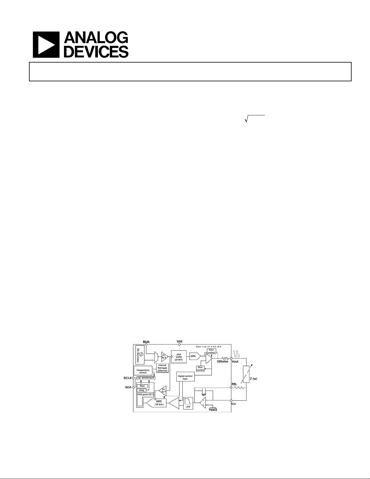
The AD5933 is a high precision impedance converter system
solution which combines an on board frequency generator with
a 12 Bit 1MSPS ADC. The frequency generator allows an
external complex impedance to be excited with a known
frequency. The response signal from the impedance is sampled
by the on board ADC and DFT processed by an on-board DSP
engine. The DFT algorithm returns a Real (R) and imaginary (I)
data word at each output frequency. This magnitude of these
data words must be further scaled by calibrated Gain Factor in
order to return the actual impedance value at each frequency
2
C loading
Network Analyzer
AD5933
point. The magnitude of the impedance and relative phase of
the impedance at each frequency point along the sweep is easily
calculated using the following equations:
122
−
)/(
=+=
To determine the value of the unknown impedance Z(w),
generally a frequency sweep is performed. The impedance can
be calculated at each point and an impedance profile i.e. frequency
vs. magnitude plot can be created. The system allows the user to
program a 2 V p-p sinusoidal signal as excitation to an external
load. Output voltage excitation ranges of 1 V, 400 mV, 200 mV
can also be programmed. The signal is provided on chip using
DDS techniques. Frequency resolution of 27 bits (less than
0.1HZ) can be achieved using this method. To perform the
frequency sweep, the user must first program the conditions
required for the sweep; start frequency, step frequency, and
number of incremental points along the sweep into onboard
registers. Once the relevant registers have been programmed, a
Start Command to the control register is required in order to
begin the sweep. To determine the impedance of the load at any
one frequency point, Z(w), a measurement system comprised of
a transimpedance amplifier, gain stage, and ADC are used to
record data. The gain stage for the response stage is 1 or 5. At
each point on the sweep the ADC will take 1024 samples and
calculate a Discrete Fourier Transform to provide the real and
imaginary data for the response signal waveform. The real and
imaginary data stored in memory and is available to the user
through the 1
2
C interface. The ADC is a low noise; high speed
1 MSPS sampling ADC that operates from 3 V supply. Clocking
for both the DDS and ADC signals is provided externally via
the MCLK reference clock, which is provided externally from a
crystal oscillator or system clock or by use of the internal RC
oscillator. The AD5933 is available in a 16 lead SSOP.
RITanPhaseIRMagnitude
Figure 1. AD5933 Block Diagram
Rev. PrB
Information furnished by Analog Devices is believed to be accurate and reliable.
However, no responsibility is assumed by Analog Devices for its use, nor for any
infringements of patents or other rights of third parties that may result from its use.
Specifications subject to change without notice. No license is granted by implication
or otherwise under any patent or patent rights of Analog Devices. Trademarks and
registered trademarks are the property of their respective owners.
One Technology Way, P.O. Box 9106, Norwood, MA 02062-9106, U.S.A.
Tel: 781.329.4700 www.analog.com
Fax: 781.326.3113 © 2005 Analog Devices, Inc. All rights reserved.

AD5933 Preliminary Technical Data
TABLE OF CONTENTS
Specifications..................................................................................... 3
Analog Channel and Filter Network........................................ 25
Timing Characteristics..................................................................... 9
Absolute Maximum Ratings.......................................................... 10
ESD Caution................................................................................ 10
Pin Configuration and Descriptions............................................ 11
Typical Performance Characteristics ........................................... 12
Terminology .................................................................................... 17
DAC/DDS core: .......................................................................... 17
ADC: ............................................................................................ 18
System Architecture Description.................................................. 19
Output Stage................................................................................ 19
DDS Core: Circuit Description ................................................ 19
Numerical Controlled Oscillator.............................................. 20
SIN ROM..................................................................................... 20
Digital-to-Analog Converter & Output Gain Stage............... 20
Response Stage............................................................................ 20
The Analog-to-Digital Converter ............................................ 25
The Discrete Fourier Transform .............................................. 25
AD5933 Discrete Fourier Transform Leakage ....................... 26
Gain Factor Calculation ............................................................ 28
AD5933 System Calibration ..................................................... 29
Performing a Frequency Sweep—Flow Chart............................ 32
Register Map (Each Row Equals 8 Bits of Data) ........................ 33
Control Register ......................................................................... 37
Control Register Decode........................................................... 38
Status Register:............................................................................ 39
Serial Bus Interface..................................................................... 40
General I
Writing/Reading to the AD5933 .............................................. 41
Block Write.................................................................................. 43
AD5933 Read Operations ......................................................... 44
2
C Timing.................................................................... 40
ADC Operation ..........................................................................21
DFT Conversion......................................................................... 21
Temperature Sensor ................................................................... 22
AD5933 Theory of Operation....................................................... 24
Oscillator Core............................................................................ 24
DDS Core..................................................................................... 24
REVISION HISTORY
3/05—Revision PrB
Error Correction......................................................................... 45
Checksum.................................................................................... 45
User Command Codes .............................................................. 45
Writing to Memory: Storing Calibration Variables............... 46
Outline Dimensions....................................................................... 49
Ordering Guide .......................................................................... 49
Rev. PrB | Page 2 of 52
Preliminary Technical Data AD5933
SPECIFICATIONS
VDD = +3.0 V ±10% T
Table 1.
Y Version
Parameter Min Typ Max Unit Test Conditions/Comments
SYSTEM SPECS
Impedance Range 0.001 10 MΩ
Total System Accuracy 1 %
System ppm 250 ppm/°C Vdd = 3. 3 V @ 25°C, 500 Hz bandwidth
MCLK Update Rate 16 MSPS System clock update rate
OUTPUT STAGE
FREQUENCY SPECS
Output Frequency Range 0 100 kHz Hz
Output Frequency
Resoltuion
MCLK External Rerference Clock.
Initial Frequency Accuracy 0.1 Hz
RC OSCILLATOR 10 16.776 17.77 MHz Internal RC Oscillator. Typically 16. 776 MHz
Initial Frequency Accuracy 1.5 %
Calibrated Frequency
Accuracy
Frequency Tempco 35 ppm/°C Requires 2 point User Calibration.
Frequency Jitter 4 Hz Jitter on VOUT Pin, 30 kHz output.
OUTPUT VOLTAGE SPECS
AC Voltage Range (div by 1) 2. 0 Volts peak to peak
Output Voltage Error 0. 9 %
DC Bias (vdd/2 ) 1.65 Volts DC bias of AC Signal vdd = 3.3 V
DC Bias Error ±9 % Tolerance of DC Bias
AC Voltage Range div by 2 1.0 Volts peak to peak
Output Voltage Error 0.8 %
DC Bias (Vdd/4) 0.79 Volts DC bias of AC Signal vdd = 3.3 V
DC Bias Error ±10 % Tolerance of DC Bias
AC Voltage Range div by 5 0.4 Volts peak to peak
Output Voltage Error 0.7 %
DC Bias (Vdd/10) 0.32 Volts DC bias of AC Signal vdd = 3.3 V
DC Bias Error ±9 % Tolerance of DC Bias
AC Voltage Range div by 10 0.2 Volts peak to peak
Output Voltage Error 0.4 %
DC Bias (Vdd/20) 0.16 Volts DC bias of AC Signal vdd = 3.3 V
DC Bias Error ±7 % Tolerance of DC Bias
MIN
to T
unless otherwise noted.
MAX
1,2
27 Bits
0.1 Hz
Uni-Polar Sinusoidal Signal at Vout. System
accuracy only guarentted in this range.
>100 kHz achievable by device but accuracy
not guarenteed.
<0.1 Hz Resolution achievable using DDS
techniques
System Output Exitation Frequency
Accuracy using external clock/crystal post
triml. 0-100 kHz Range.
System Output Exitation Frequency
Accuracy using internal clock oscillator post
trim. 0-100 kHz Range.
0-100 kHz Range.
1 point Offset Calibration
Pk-Pk Unipolar output excitation Voltage on
VOut. Vdd = 3.3 V
Voltage Error on Pk-Pk Output Excitation
voltage. Vdd = 3.3 V
Pk-Pk Unipolar output excitation Voltage on
VOut. Vdd = 3.3 V
Voltage Error on Pk-Pk Output excitation
voltage. Vdd = 3.3 V
Pk-Pk Unipolar output excitation Voltage on
VOut. Vdd = 3.3 V
Voltage Error on Pk-Pk Output excitation
voltage. Vdd = 3.3 V
Pk-Pk Unipolar output excitation Voltage on
VOut. Vdd = 3.3 V
Voltage Error on Pk-Pk Output excitation
voltage. Vdd = 3.3 V
Rev. PrB | Page 3 of 52
AD5933 Preliminary Technical Data
Y Version
Parameter Min Typ Max Unit Test Conditions/Comments
DC Output Impedance
(at Vout)
DC Output Impedance 2.4 kΩ
DC Output Impedance 1 kΩ
DC Output Impedance 600 Ω
Short Circuit Current
(at Vout)
Short Circuit Current ±1 mA
Short Circuit Current ±2.5 mA
Short Circuit Current ±4.5 mA
AC CHARACTERISTICS
Signal to Noise Ratio 60 dB
Total Harmonic Distortion −52 dB
−52 dB
Spurious free Dynamic
Range (SFDR)
Wideband (0 to 1 MHz) 56 dB
56 dB
Narrowband (± 5 kHz) 85 dB
80 dB
Clock Feedthrough
(0 to 17 MHz)
SYSTEM RESPONSE STAGE
ANALOG INPUT VIN
Input Leakage Current 1 nA To Pin VIN
Input Capacitance 3.5 pF
Input Impedance 68.5G Ω
ADC ACCURACY
Resolution 12 Bits
Sampling Rate 1 MSPS
Integral Nonlinearity ±1 LSB No missing Codes
Differential Nonlinearity ±1 LSB Guarentted monitonic
400 Ω
±7 mA
−60 dB
1,2
2.0Vp-p, Output frequency = 30 kHz
(external oscillator), vdd = 3.3 V, Ta = 25°C
1.0 Vp-p, Output frequency = 30 kHz
(external oscillator), vdd = 3.3 V, Ta = 25°C
400 mVp-p, Output frequency = 30 kHz,
(external oscillator) vdd = 3.3 V, Ta = 25°C
200 mVp-p, Output frequency = 30 kHz
(external oscillator), vdd = 3.3 V, Ta = 25°C
2.0 Vp-p, Output frequency = 30 kHz
(external oscillator), vdd = 3.3 V, Ta = 25°C
2.0 Vp-p, Output frequency = 30 kHz
(external oscillator), vdd = 3.3 V, Ta = 25°C
2.0 Vp-p, Output frequency = 30 kHz
(external oscillator), vdd = 3.3 V, Ta = 25°C
2.0 Vp-p, Output frequency = 30 kHz
(external oscillator), vdd = 3.3 V, Ta = 25°C
Output excitation voltage = 30 kHz, external
oscillator mclk = 16.776 MHz, Ta = 25°C
vdd =3.3 V
Output excitation voltage = 30kHz, external
oscillator mclk = 16.776 MHz, Ta = 25°C
vdd = 3.3 V
Output excitation voltage = 30kHz, internal
oscillator mclk = 16.776 MHz, Ta = 25°C vdd
=3.3 V
Output excitation voltage = 30 kHz, external
oscillator mclk = 16.776 MHz, Ta = 25°C
vdd =3.3 V
Output excitation voltage = 30kHz, internal
oscillator mclk = 16.776 MHz, Ta = 25°C
vdd = 3.3 V
Output excitation voltage = 30kHz, external
oscillator mclk = 16.776 MHz, Ta = 25°C
vdd = 3.3 V
Output excitation voltage = 30 kHz, internal
oscillator mclk = 16.776 MHz, Ta = 25°C
vdd = 3.3 V
Output excitation voltage = 30 kHz, external
oscillator mclk = 16.776 MHz, Ta = 25°C
vdd = 3.3 V
Pin capacitance between Vout and Gnd.
Vdd = 3.3 V @25°C
Input impedance between Vout and Gnd.
vdd = 3.3 V @25°C. No feedback resistor
connected.
Rev. PrB | Page 4 of 52
Preliminary Technical Data AD5933
Y Version
1,2
Parameter Min Typ Max Unit Test Conditions/Comments
Offset Error ±3 LSB
Gain Error ±6 LSB
TEMPERATURE SENSOR
Accuracy ±1 °C Ta = −40°C to 125°C
Resolution 0.03125 °C
Auto Conversion Update
1 sec Temperature measurement every 1 second
Rate
Temperature Conversion
800 µs Vdd = 3.3 V
Time
LOGIC INPUTS
Vih, Input High Voltage 2.3 VDD = 3 V
Vil, Input Low Voltage 0.9 VDD = 3 V
Input Current ±4.2 µA Vdd = 3.3 V, Ta = 25°C,
Input Capacitance 7 pF Vdd = 3.3 V, Ta = 25°C
POWER REQUIREMENTS
Vdd 3.3 Volts
IDD (Normal Mode) 9 mA Digital and analog supply currents
IDD (Powerdown Mode) 0.7 µA Digital and analog supply currents
1
Temperature ranges are as follows: Y version = −40°C to +125°C, typical at 25°C.
2
Guaranteed by design and characterization, not production tested.
Rev. PrB | Page 5 of 52

AD5933 Preliminary Technical Data
VDD = +5.0 V ±10% T
Table 2.
Y Version
Parameter Min Typ Max Unit Test Conditions/Comments
SYSTEM SPECS
Impedance Range 0.001 10 MΩ
Total System Accuracy 1 %
System ppm 250 ppm/°C Vdd = 5. 5v@25°C, 500Hz bandwidth
MCLK Update Rate 16 MSPS System clock update rate
OUTPUT STAGE
FREQUENCY SPECS
Output Frequency Range 0 100KHz Hz
Output Frequency
Resoltuion
MCLK External Rerference Clock.
Initial Frequency Accuracy 0.1 Hz
RC OSCILLATOR 10 16.776 17.77 MHz Internal RC Oscillator. Typically 16. 776 MHz
Initial Frequency Accuracy 1.5 %
Calibrated Frequency
Accuracy
Frequency Tempco 35 ppm/°C Requires 2 point User Calibration.
Frequency Jitter 4 Hz Jitter on VOUT Pin, 30KHz output.
OUTPUT VOLTAGE SPECS
AC Voltage Range div by 1 2.0 Volts peak to peak
Output Voltage Error 0.9 %
DC Bias (vdd/2 ) 1.65 Volts DC bias of AC Signal vdd = 5. 5v
DC Bias Error ±9 % Tolerance of DC Bias
AC Voltage Range div by 2 1.0 Volts peak to peak
Output Voltage Error 0. 8 %
DC Bias (Vdd/4) 0.79 Volts DC bias of AC Signal vdd = 5. 5v
DC Bias Error ±10 % Tolerance of DC Bias
AC Voltage Range div by 5 0.4 Volts peak to peak
Output Voltage Error 0.7 %
DC Bias (Vdd/10) 0.32 Volts DC bias of AC Signal vdd = 5. 5v
DC Bias Error ±9 % Tolerance of DC Bias
AC Voltage Range div by
10
Output Voltage Error 0.4 %
DC Bias (Vdd/20) 0.16 Volts DC bias of AC Signal vdd = 5. 5v
DC Bias Error ±7 % Tolerance of DC Bias
DC Output Impedance
(at Vout)
MIN
to T
unless otherwise noted.
MAX
1,2
27 Bits
0.1 Hz
0.2 Volts peak to peak
400 Ω
Uni-Polar Sinusoidal Signal at Vout.System
accuracy only guarentted in this range. >100kHz
achievable by device but accuracy not
guarenteed.
<0.1 Hz Resolution achievable using DDS
techniques
System Output Exitation Frequency Accuracy
using external clock/crystal post triml. 0 -100KHz
Range.
System Output Exitation Frequency Accuracy
using internal clock oscillator post trim. 0 100KHz Range.
0-100KHz Range.
1 point Offset Calibration
Pk-Pk Unipolar output excitation Voltage on
VOut. Vdd = 5. 5v
Voltage Error on Pk-Pk Output Excitation
voltage. Vdd = 5. 5v
Pk-Pk Unipolar output excitation Voltage on
VOut. Vdd = 5. 5v
Voltage Error on Pk-Pk Output excitation
voltage. Vdd = 5. 5v
Pk-Pk Unipolar output excitation Voltage on
VOut. Vdd = 5. 5v
Voltage Error on Pk-Pk Output excitation
voltage. Vdd = 5. 5v
Pk-Pk Unipolar output excitation Voltage on
VOut. Vdd = 5. 5v
Voltage Error on Pk-Pk Output excitation
voltage. Vdd = 5. 5v
2.0 Vp-p, Output frequency = 30 kHz (external
oscillator), vdd= 5. 5v, Ta= 25°C
Rev. PrB | Page 6 of 52
Preliminary Technical Data AD5933
Y Version
Parameter Min Typ Max Unit Test Conditions/Comments
DC Output Impedance 2.4 kΩ
DC Output Impedance 1 kΩ
DC Output Impedance 600 Ω
Short Circuit Current
(at Vout)
Short Circuit Current ±1 mA
Short Circuit Current ±2.5 mA
Short Circuit Current ±4.5 mA
AC CHARACTERISTICS
Signal to Noise Ratio 60 dB
Total Harmonic Distortion −52 dB
−52 dB
Spurious free Dynamic
Range (SFDR)
Wideband (0 to 1 MHz) 56 dB
56 dB
Narrowband (± 5 kHz) 85 dB
80 dB
Clock Feedthrough (0 to 17
MHz)
SYSTEM RESPONSE STAGE
ANALOG INPUT VIN
Input Leakage Current 1 nA To Pin VIN
Input Capacitance 3.5 pF
Input Impedance 68.5G Ω
ADC ACCURACY
Resolution 12 Bits
Sampling Rate 1 MSPS
Integral Nonlinearity ±1 LSB No missing Codes
Differential Nonlinearity ±1 LSB Guaraunted monitonic
Offset Error
Gain Error
±7 mA
−60 dB
1,2
1.0 Vp-p, Output frequency = 30 kHz (external
oscillator), vdd = 5. 5v, Ta= 25°C
400 mVp-p, Output frequency = 30 kHz, (external
oscillator) vdd = 5. 5v, Ta= 25°C
200 mVp-p, Output frequency = 30 kHz (external
oscillator), vdd = 5. 5v, Ta= 25°C
2.0 Vp-p, Output frequency = 30 kHz (external
oscillator), vdd = 5. 5v, Ta= 25°C
2.0 Vp-p, Output frequency = 30 kHz (external
oscillator), vdd = 5. 5v, Ta= 25°C
2.0 Vp-p, Output frequency = 30 kHz (external
oscillator), vdd = 5. 5v, Ta= 25°C
2.0Vp-p, Output frequency = 30 kHz (external
oscillator), vdd = 5. 5 V, Ta= 25°C
Output excitation voltage = 30 kHz, external
oscillator mclk = 16.776 MHz, Ta = 25°C
vdd = 5.5 V
Output excitation voltage = 30kHz, external
oscillator mclk = 16.776 MHz, Ta = 25°C vdd = 5.
5v
Output excitation voltage = 30 kHz, internal
oscillator mclk = 16.776 MHz, Ta = 25°C
vdd = 5.5 V
Output excitation voltage = 30 kHz, external
oscillator mclk = 16.776 MHz, Ta = 25°C
vdd = 5.5 V
Output excitation voltage = 30 kHz, internal
oscillator mclk = 16.776 MHz, Ta = 25°C
vdd = 5.5 V
Output excitation voltage = 30kHz, external
oscillator mclk = 16.776 MHz, Ta = 25°C vdd = 5.
5v
Output excitation voltage = 30 kHz, internal
oscillator mclk = 16.776 MHz, Ta = 25°C
vdd = 5.5 V
Output excitation voltage = 30kHz, external
oscillator mclk = 16.776 MHz, Ta = 25°C
vdd = 5.5 V
Pin capacitance between VouT and Gnd = 5. 5 V
@25°C
Input impedance between Vout and Gnd = 5. 5v
@25°C. No feedback resistor connected.
Rev. PrB | Page 7 of 52

AD5933 Preliminary Technical Data
Y Version
1,2
Parameter Min Typ Max Unit Test Conditions/Comments
TEMPERATURE SENSOR
Accuracy ±1 °C Ta = −40 °C to 125° c
Resolution 0.03125 °C
Auto Conversion Update
1 sec Temperature measurement every 1 sec
Rate
Temperature Conversion
800 uS Vdd = 5. 5v
Time
LOGIC INPUTS
Vih, Input High Voltage 2.3 VDD = 3v
Vil, Input Low Voltage 0.9 VDD = 3V
Input Current ±4. 2 uA Vdd = 5. 5v,Ta =25°C,
Input Capacitance 7 pF Vdd = 5. 5v,Ta = 25°C
POWER REQUIREMENTS
Vdd 3. 3 Volts
IDD (Normal Mode) 9 mA Digital and analog supply currents
IDD (Powerdown Mode) 0.7 uA Digital and analog supply currents
1
Temperature ranges are as follows: Y version = −40°C to +125°C, typical at 25°C.
2
Guaranteed by design and characterization, not production tested.
Rev. PrB | Page 8 of 52
Preliminary Technical Data AD5933
TIMING CHARACTERISTICS
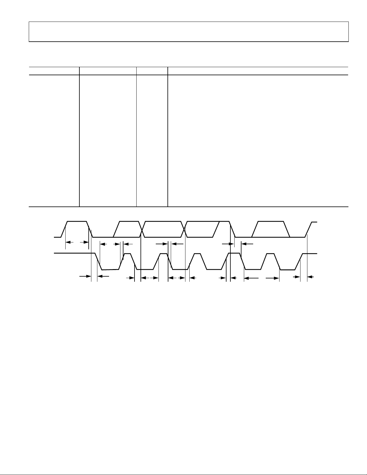
Table 3. I2C Serial Interface
Parameter Limit at T
F
1483 kHz max SCL clock frequency
SCL
t1 0.7 µs min SCL cycle time
t2 0. 2 µs min t
t3 0. 6 µs min t
t4 0.6 µs min tHD,
t5 3 ns min tSU,
t6 0.9 µs max tHD,
0 µs min tHD,
t7 0.007 µs min tSU,
t8 0.6 µs min tSU,
t9 0.161 µs min t
t10 55 ns max tF, fall time of SDA when transmitting
0 ns min tR, rise time of SCL and SDA when receiving (CMOS compatible)
t11 300 ns max tF, fall time of SDA when transmitting
0 ns min tF, fall time of SDA when receiving (CMOS compatible)
300 ns max tF, fall time of SCL and SDA when receiving
20 + 0.1 CB ns min tF, fall time of SCL and SDA when transmitting
CB 400 pF max Capacitive load for each bus line
MIN
, T
Unit Description
MAX
, SCL high time
HIGH
, SCL low time
LOW
, start/repeated start condition hold time
STA
, data setup time
DAT
data hold time
DAT
data hold time
DAT
setup time for repeated start
STA
stop condition setup time
STO
, bus free time between a stop and a start condition
BUF
SDA
t
SCL
9
t
START
CONDITION
t
3
4
t
t
11
10
t
6
t
2
Figure 2. I
t
t
5
7
2
C Interface Timing Diagram
t
4
REPEATED
START
CONDITION
t
1
t
8
STOP
CONDITION
03773-0-007
Rev. PrB | Page 9 of 52

AD5933 Preliminary Technical Data
ABSOLUTE MAXIMUM RATINGS
TA = 25°C, unless otherwise note
Table 4.
Parameter Rating
VDD to GND −0.3 V to +7. 0 V
Digital Input Voltage to GND −0.3 V to VDD + 0.3 V
V
to GND −0.3 V to VDD + 0.3 V
OUT
Vin to GND −0.3 V to VDD + 0.3 V
Operating Temperature Range
Extended Industrial (Y grade) −40°C to +125°C
Storage Temperature Range −65°C to +160°C
Maximum Junction Temperature 150°C
uSOIC Package
θJA Thermal Impedance 332°C/W
θJC Thermal Impedance 120°C/W
Lead Temperature, Soldering
Vapor Phase (60 sec) 215°C
Infrared (15 sec) 220°C
ESD 2.0 kV
Stresses above those listed under Absolute Maximum Ratings
may cause permanent damage to the device. This is a stress
rating only; functional operation of the device at these or any
other conditions above those listed in the operational sections
of this specification is not implied. Exposure to absolute
maximum rating conditions for extended periods may affect
device reliability.
ESD CAUTION
ESD (electrostatic discharge) sensitive device. Electrostatic charges as high as 4000 V readily accumulate on
the human body and test equipment and can discharge without detection. Although this product features
proprietary ESD protection circuitry, permanent damage may occur on devices subjected to high energy
electrostatic discharges. Therefore, proper ESD precautions are recommended to avoid performance
degradation or loss of functionality.
Rev. PrB | Page 10 of 52

Preliminary Technical Data AD5933
PIN CONFIGURATION AND DESCRIPTIONS
1
N/C
2
N/C
N/C
3
4
AD5933
5
VIN
TOP VIEW
(Not to Scale)
VOUT
6
N/C
7
8
MCLK
Figure 3. Pin Configuration
Table 5. Pin Function Descriptions
Mnemonic Description
N/C No Connect.
RFB_PIN External Feedback Resistor. This is used to set the gain of the input signal of the VIN node.
VOUT Input Signal to transimpedance amplifier. External Feedback resistor will control gain of transimpedance amplifier
MCLK Master Clock for the system. Used to provide output excitation signal and as sampling of ADC.
DVDD Digital Supply Voltage
AVDD1 Analog Supply Voltage 1
AVDD2 Analog Supply Voltage 2
DGND Digital Ground
AGND1 Analog Gnd 1
AGND2 Analog Gnd 2
SDA I2C Data Input
SCL I2C Clock Input.
Table 6. Recommended Pin Connections for AD5933
Mnemonic Function
Pin 1 Ext_Out Test Pin—Leave unconnected
Pin 2 NC No Connect—Do not apply any signal
Pin 3 NC No Connect—Do not apply any signal
Pin4 NC No Connect—Do not apply any signal.
Pin5 Vin (Receive side of impedance) Test Impedance is connected between this pin and vout pin
Pin6 Vout (Excitation side of impedance) Test Impedance is connected between this pin and vin pin
Pin 7 NC No Connect—Do not apply any signal
Pin 8 Ext_Clk Extclk Pad—Only used if external clk option is selected
Pin 9 AVDD1 Recommended to be tied to 3.3V
Pin10 AVDD2 Recommended to be tied to 3.3V
Pin11 DVDD Recommended to be tied to 3.3V
Pin12 DGND Must be tied to GND
Pin13 AGND1 Must be tied to GND
Pin14 AGND2 Must be tied to GND
Pin15 SDA I2C Data Pin
Pin16 SCL I2C Clk Pin
16
15
14
13
12
11
10
9
SCL
SDA
AGND2
AGND1RFB_PIN
DGND
AVD D2
AVDD 1
DVDD
It is recommended to tie all supply connections (Pins 9, 10, 11) and run from a single supply between 3. 0 V and 5.5 V. Also, it is
recommended to connect all ground signals together (Pins 12, 13, 14).
Rev. PrB | Page 11 of 52
AD5933 Preliminary Technical Data
TYPICAL PERFORMANCE CHARACTERISTICS
1.00E-06
Ta = 25°C
Vdd = 3.3v
Rfb = 1k, 0.5k impedance
1.00E-07
1.00E-08
Gain Factor
1.00E-09
1.00E-10
0 20000 40000 60000 80000 100000
Rfb = 1k, 1k impedance
Rfb = 10k, 10k impedance
Rfb = 50k, 50k impedance
Rfb = 100k, 100k impedance
Rfb = 1M, 1M impedance
Frequency (Hz)
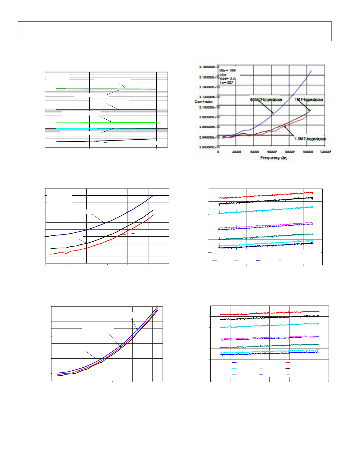
Figure 4. Gain Factor vs. Frequency for Various Rfb/Impedance Ranges
2.000E-08
1.980E-08
1.960E-08
1.940E-08
1.920E-08
1.900E-08
1.880E-08
Gain Factor
1.860E-08
1.840E-08
1.820E-08
1.800E-08
1.780E-08
Rfb = 1k ohm
Vdd = 3.3v
Ta = 25°C
5KΩ impedance
15KΩ impedance
10KΩ impedance
0 20000 40000 60000 80000 100000 120000
Frequency (Hz)
Figure 5. Gain Factor vs. Frequency for 5 Ωk to 15 kΩ Impedance Range
Figure 7. Gain Factor vs. Frequency for 500 kΩ to 1.5 MΩ Impedance Range
1.03E+03
1.02E+03
1.01E+03
1.00E+03
Impedance (Ohm)
9.90E+02
9.80E+02
9.70E+02
2.7V -40C
3.3V 125C
94.0E+3 96.0E+3 98.0E+3 100.0E+3 102.0E+3 104.0E+3 106.0E+3
2.7V 25C
5.5V -40C
2.7V 125C
5.5V 25C
Frequency (Hz)
3.3V -40C
5.5V 125C
3.3V 25C
Figure 8. Impedance vs. Frequency for a 1kΩ Rfb Impedance, Gain Factor @100 kHz
2.200E-09
Rfb = 10k ohm
Vdd = 3.3v
2.180E-09
Ta = 25°C
2.160E-09
2.140E-09
2.120E-09
2.100E-09
2.080E-09
gain factor
2.060E-09
2.040E-09
2.020E-09
2.000E-09
150KΩ impedance
0 20000 40000 60000 80000 100000
100KΩ impedance
50KΩ impedance
Frequency (hz)
Figure 6. Gain Factor vs. Frequency for 50 kΩ to 150 kΩ Impedance Range
Rev. PrB | Page 12 of 52
1.03E+03
1.02E+03
1.01E+03
1.00E+03
9.90E+02
Impedance (ohms)
9.80E+02
9.70E+02
9.60E+02
54000 56000 58000 60000 62000 64000 66000
2.7V -40C
3.3V -40C
5.5V -40C
2.7V 25C
3.3V 25C
5.5V 25C
Frequency (Hz)
2.7V 125C
3.3V 125C
5.5V 125C
Figure 9. Impedance vs. Frequency for a 1 kΩ Rfb, impedance, Gain Factor @ 60 kHz
Preliminary Technical Data AD5933
0
1.03E+03
1.02E+04
1.02E+03
1.01E+03
1.00E+03
9.90E+02
Impedance ( ohm )
9.80E+02
9.70E+02
29000 31000 33000 35000 37000 39000 41000
2.7 -40C
3.3v -40C
5.5 -40C
2.7 25C
3.3 25C
5.5 25C
Frequency (Hz)
2.7 125
3.3 125C
5.5 125C
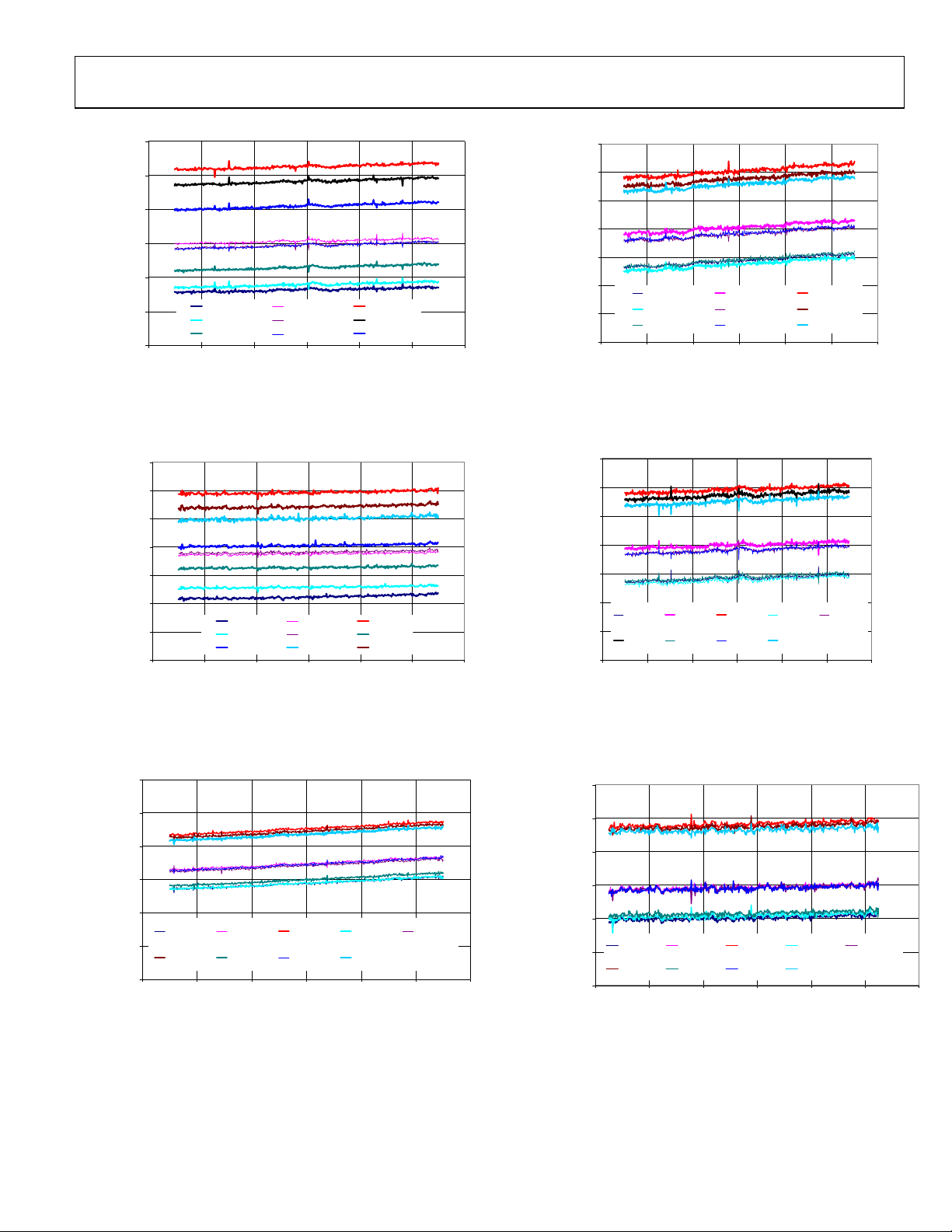
Figure 10. Impedance vs. Frequency 1 kΩ Rfb, Impedance, Gain Factor @ 35 kHz
1.03E+03
1.02E+03
1.01E+03
1.00E+03
9.90E+02
Impedance ( ohm )
9.80E+02
9.70E+02
9.60E+02
4.00E+03 6.00E+03 8.00E+03 1.00E+04 1.20E+04 1.40E+04 1.60E+04
2.7 -40
3.3 -40
5.5 25
2.7 25
3.3 25
5.5 125
Frequency (Hz)
2.7 125
5.5 -40
3.3 125
Figure 11. Impedance vs. Frequency 1 kΩ Rfb, Impedance, Gain Factor @ 10 kHz
1.01E+04
1.01E+04
1.00E+04
9.95E+03
Impedance
9.90E+03
9.85E+03
9.80E+03
54000 56000 58000 60000 62000 64000 66000
2.7V -40C
3.3V -40C
5.5V -40C
2.7V 25C
3.3V 25C
5.5V 25C
Frequency (Hz)
2.7V 125C
3.3V 125C
5.5V 125C
Figure 13. Impedance vs. Frequency 10 kΩ Rfb, Impedance, Gain Factor @ 60 kHz
1.02E+04
1.01E+04
1.01E+04
1.00E+04
9.95E+03
Impedance
9.90E+03
9.85E+03
9.80E+03
2.7V -40C
3.3V 125C
29000 31000 33000 35000 37000 39000 41000
2.7V 25C
5.5V -40C
2.7V 125C
5.5V 25C
Frequency (Hz)
3.3V -40C
5.5V 125C
3.3V 25C
Figure 14. Impedance vs. Frequency 10 kΩ Rfb, Impedance, Gain Factor @ 35 kHz
1.03E+04
1.02E+04
1.01E+04
9.95E+03
Impedance (Ohm)
9.85E+03
9.75E+03
9.65E+03
2.7V -40C 2.7V 25C 2.7V 125C 3.3V -40C 3.3V 25C
3.3V 125C 5.5V -40C 5.5V 25C 5.5V 125C
94.0E+3 96.0E+3 98.0E+3 100.0E+3 102.0E+3 104.0E+3 106.0E+3
Frequency (Hz)
Figure 12. Impedance vs. Frequency 10 kΩ Rfb, Impedance, Gain Factor @ 100 kHz
1.02E+04
1.01E+04
1.01E+04
1.00E+04
Impedance
9.95E+03
9.90E+03
9.85E+03
2.7V -40C
3.3V 125C
4500 6500 8500 10500 12500 14500 1650
2.7V 25C
5.5V -40C
2.7V 125C
5.5V 25C
Frequency (Hz)
3.3V -40C
5.5V 125C
3.3V 25C
Figure 15. Impedance vs. Frequency 10 kΩ Rfb, Impedance, Gain Factor @ 10 kHz
Rev. PrB | Page 13 of 52
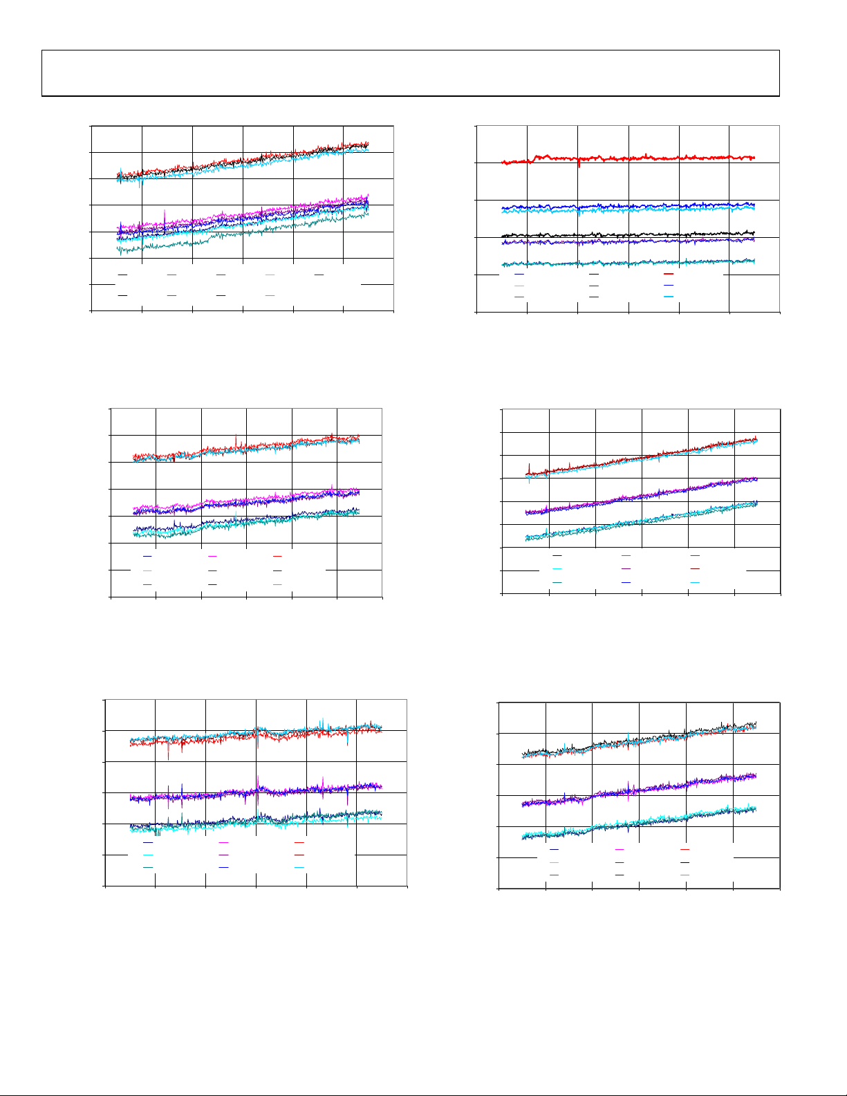
AD5933 Preliminary Technical Data
0
0
0
50600
51500
50400
50200
50000
49800
Impedance
49600
49400
49200
94000 96000 98000 100000 102000 104000 106000
2.7V -40C 2.7V 25C 2.7V 125C 3.3V -40C 3.3V 25C
3.3V 125C 5.5V -40C 5.5V 25C 5.5V 125C
Frequency
Figure 16. Impedance vs. Frequency 50 kΩ Rfb, Impedance, Gain Factor @ 100 kHz
5.06E+04
5.04E+04
5.02E+04
5.00E+04
4.98E+04
Impedance
4.96E+04
4.94E+04
4.92E+04
54000 56000 58000 60000 62000 64000 66000
2.7V -40C
3.3V -40C
5.5V -40C
2.7V 25C
3.3V 25C
5.5V 25C
Frequency (Hz)
2.7V 125C
3.3V 125C
5.5V 125C
Figure 17. Impedance vs. Frequency 50 kΩ Rfb, Impedance, Gain Factor @ 60 kHz
51000
50500
Impedance
50000
49500
49000
4000 6000 8000 10000 12000 14000 16000
2.7V -40C 2.7V 25C 2.7V 125C
3.3V -40C 3.3V 25C 3.3V 125C
5.5V -40C 5.5V 25C 5.5V 125C
Frequency (Hz)
Figure 19. Impedance vs. Frequency 50 kΩ Rfb, Impedance, Gain Factor @ 10 kHz
1.02E+05
1.02E+05
1.01E+05
1.01E+05
1.00E+05
Impedance
9.95E+04
9.90E+04
9.85E+04
9.80E+04
9.40E+04 9.60E+04 9.80E+04 1.00E+05 1.02E+05 1.04E+05 1.06E+
2.7V -40C
3.3V -40C
5.5V -40C
2.7V 25C
3.3V 25C
5.5V 25C
Frequency (Hz)
2.7V 125C
3.3V 125C
5.5V 125C
Figure 20. Impedance vs. Frequency 100 kΩ Rfb, Impedance, Gain Factor @ 100 kHz
5.05E+04
5.03E+04
5.01E+04
4.99E+04
Impedance
4.97E+04
4.95E+04
4.93E+04
29000 31000 33000 35000 37000 39000 4100
2.7V -40C
3.3V -40C
5.5V -40C
2.7V 25C
3.3V 25C
5.5V 25C
Frequency (Hz)
2.7V 125C
3.3V 125C
5.5V 125C
Figure 18. Impedance vs. Frequency 50 kΩ Rfb, Impedance, Gain Factor @ 35 kHz
1.02E+05
1.01E+05
1.01E+05
1.00E+05
Impedance
9.95E+04
9.90E+04
9.85E+04
54000 56000 58000 60000 62000 64000 660
2.7V -40C
3.3V -40C
5.5V -40C
2.7V 25C
3.3V 25C
5.5V 25C
Frequency ( Hz)
2.7V 125C
3.3V 125C
5.5V 125C
Figure 21. Impedance vs. Frequency 100 kΩ Rfb, Impedance, Gain Factor @ 60 kHz
Rev. PrB | Page 14 of 52
Preliminary Technical Data AD5933
1.02E+05
5.30E+05
1.01E+05
1.01E+05
1.00E+05
Impedance
9.95E+04
9.90E+04
9.85E+04
29000 31000 33000 35000 37000 39000 41000
2.7V -40C 2.7V 25C 2.7V 125C
3.3V -40C 3.3V 25C 3.3V 125C
5.5V -40C 5.5V 25C 5.5V 125C
Frequency (Hz)
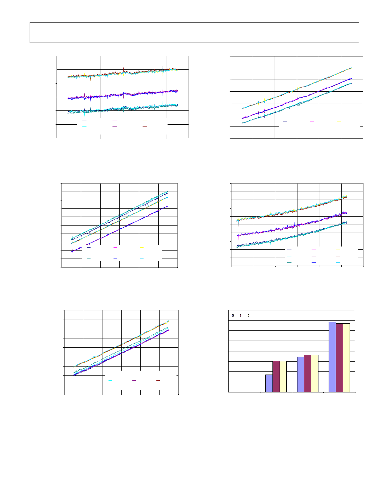
Figure 22. Impedance vs. Frequency 100 kΩ Rfb, Impedance, Gain Factor @ 35 kHz
540000
535000
530000
525000
520000
515000
Impedance
510000
505000
500000
495000
490000
9.40E+04 9.60E+04 9.80E+04 1.00E+05 1.02E+05 1.04E+05 1.06E+05
2.7V -40C
3.3V -40C
5.5V -40C
2.7V 25C
3.3V 25C
5.5V 25C
Frequency (Hz)
2.7V 125C
3.3V 125C
5.5V 125C
Figure 23. Impedance vs. Frequency 500 kΩ Impedance, Gain Factor @ 100 kHz
5.25E+05
5.20E+05
5.15E+05
5.10E+05
Impedance
5.05E+05
5.00E+05
4.95E+05
29000 31000 33000 35000 37000 39000 41000
2.7V -40C 2.7V 25C 2.7V 125C
3.3V -40C 3.3V 25C 3.3V 125C
5.5V -40C 5.5V 25C 5.5V 125C
Frequency (Hz)
Figure 25. Impedance vs. Frequency 500 kΩ Impedance, Gain Factor @ 35 kHz
5.22E+05
5.20E+05
5.18E+05
5.16E+05
5.14E+05
5.12E+05
Impedance
5.10E+05
5.08E+05
5.06E+05
5.04E+05
5.02E+05
4500 6500 8500 10500 12500 14500 16500
2.7V -40C 2.7V 25C 2.7V 125C
3.3V -40C 3.3V 25C 3.3V 125C
5.5V -40C 5.5V 25C 5.5V 125C
Frequency (Hz)
Figure 26. Impedance vs. Frequency 500 kΩ Impedance, Gain Factor @ 10 kHz
5.35E+05
5.30E+05
5.25E+05
5.20E+05
5.15E+05
5.10E+05
Impedance
5.05E+05
5.00E+05
4.95E+05
4.90E+05
54000 56000 58000 60000 62000 64000 66000
2.7V -40C
3.3V -40C
5.5V -40C
Frequency (Hz)
2.7V 25C
3.3V 25C
5.5V 25C
2.7V 125C
3.3V 125C
5.5V 125C
Figure 24. Impedance vs. Frequency 500 kΩ Impedance, Gain Factor @ 60 kHz
Rev. PrB | Page 15 of 52
0.8
2.7V
3.3V
0.7
0.6
0.5
0.4
% Error
0.3
0.2
0.1
0
5.5V
10kHz 35kHz 60kHz 100kHz
Frequency
Figure 27. Impedance Error over 10 kHz to 100 kHz Range, Gain Factor @ 10 kHz
AD5933 Preliminary Technical Data
0.4
vdd = 3.3
Ta =25°C
Freq = 32khz
0.2
0
-0.2
-0.4
phase error (degrees)
-0.6
-0.8
-1
0 50 100 150 200 250 300 350 400
Phase (degrees)
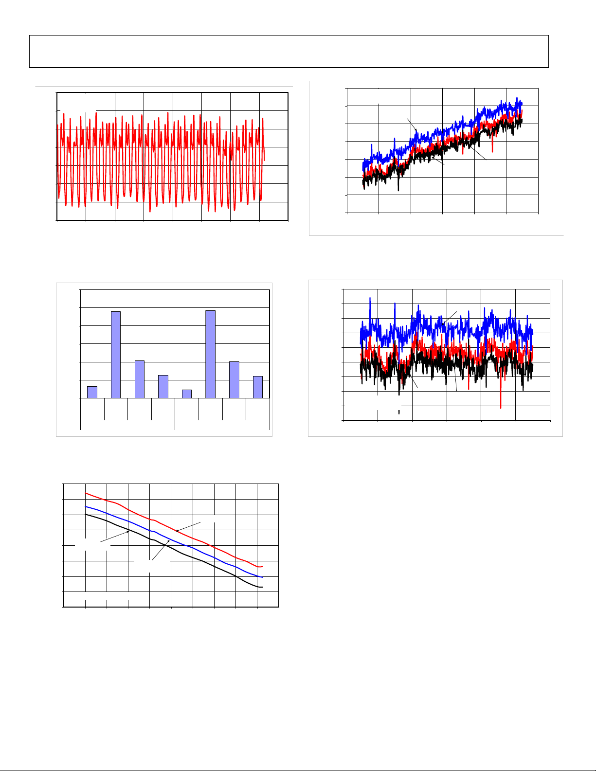
Figure 28. Typical AD5933 Phase Error
50.1E+3
Rf = 50kΩ
impedance = 50kΩ
50.0E+3
50.0E+3
49.9E+3
49.9E+3
Impedance (Ohm)
49.8E+3
49.8E+3
49.7E+3
54.0E+3 56.0E+3 58.0E+3 60.0E+3 62.0E+3 64.0E+3 66.0E+3
vdd = 5.5v
vdd = 3.3v vdd = 2.7v
Frequency (Hz)
Figure 31. Typical Impedance e vs. Frequency for 49.992 kΩ Impedance,
Single Point Calibrated Gain Factor @ 60 kHz
3.0E+3
2.5E+3
2.0E+3
1.5E+3
1.0E+3
Impedance (Ohm)
500.0E+0
000.0E+0
k
k
k
k
P
P
V
4
.
0
k
P
P
-
-
k
k
P
V
0
2
.
.
2
0
DDS Output Voltag e Range
P
P
-
-
k
k
P
P
V
.
1
V
V
0
4
.
0
k
P
-
k
k
P
P
V
V
0
0
.
.
2
1
Vdd 3.3V Vdd 5.5V
Figure 29. Typical AD5933 Output Impedance
30.4E+3
30.4E+3
30.3E+3
30.3E+3
30.2E+3
Frequency (Hz)
30.2E+3
30.1E+3
30.1E+3
30.0E+3
vdd = 3.3
vdd = 3.3
output freq = 30khz @25°
-60 -40 -20 0 20 40 60 80 100 120 140
C
Temperature (degree C)
vdd = 5.5v
Figure 30. Typical AD5933 Frequency Temperature Coefficient
50.0E+3
50.0E+3
49.9E+3
49.9E+3
49.9E+3
49.9E+3
Impedance (ohm)
49.9E+3
49.8E+3
Rf = 50kΩ
impedance = 50kΩ
k
k
P
P
-
-
k
k
P
P
V
2
.
0
49.8E+3
49.8E+3
54.0E+3 56.0E+3 58.0E+3 60.0E+3 62.0E+3 64.0E+3 66.0E+3
vdd = 3.3v
vdd = 5.5v
vdd = 2.7v
Frequency (Hz)
Figure 32. Typical Impedance e vs. Frequency for 49.992 kΩ Impedance,
End Point Calibrated Gain Factor
Rev. PrB | Page 16 of 52
 Loading...