

Programmable Single-Scan
Preliminary Technical Data
FEATURES
Programmable frequency profile—no external components
necessary
Ouput frequency up to 25 Mhz
Predefined frequency profile minimizes number of
DSP/µcontroller writes
Sinusoidal/triangular/square wave outputs
Powerdown mode (20 µA)
+2.3 V to +5.5 V power supply
Extended temperature range −40°C to +105°C
16-pin TSSOP
APPLICATIONS
Frequency Scan
Network/Impedance Measurements
Incremental Frequency stimulus
Sensory Applications—Proximity and Motion
BFSK
Waveform Generator
AD5932*
GENERAL DESCRIPTION
The AD5932 is a waveform generator providing a
programmable frequency scan. Utilizing embedded digital
processing allowing enhanced frequency control the device
generates synthesized analog or digital frequency-stepped
waveforms. Because frequency profiles are preprogrammed
continuous write cycles are eliminated, thereby freeing up
valuable DSP/µController resources. Waveforms start from a
known phase and are incremented phase continuously allowing
phase shifts to be easily determined. Consuming only 8mA the
AD5932 provides a convenient low power solution to waveform
generation.
To program the device, the user enters the start frequency, the
increment step size, the number of increments to be made and
the time interval the part stays at each frequency. The frequency
profile can be initiated by toggling the CTRL pin.
(continued on Page 3)
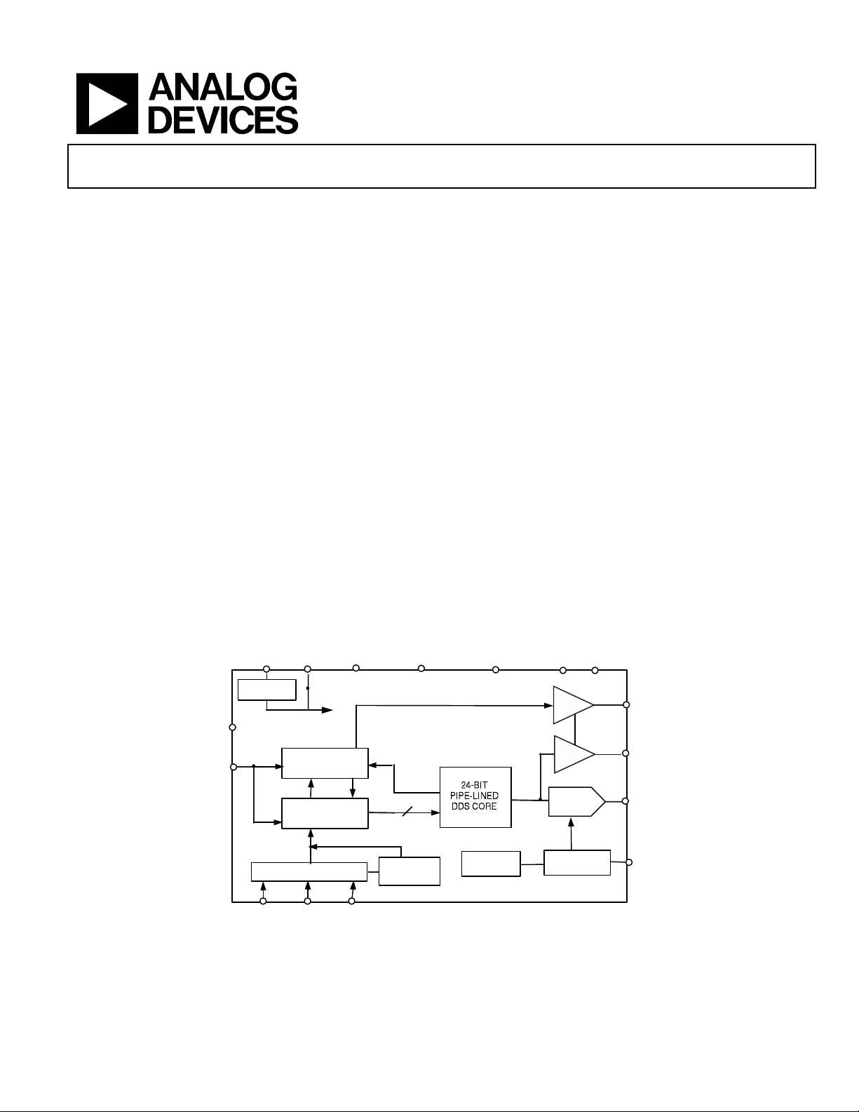
FUNCTIONAL BLOCK DIAGRAM
CAP/2.5VDVDD
REGULATOR
MCLK
CTRL
FSYNC
*Protected by US Patent Number 6747583, other patents pending
INCREMENT
CONTROLLER
DATA
FREQUENCY
CONTROLLER
DATA
SERIAL INTERFACE
SCLK SDATA
DGND
VCC
2.5V
INCR
& CONTROL
SYNC
INTERUPT
24
CONTROL
REGISTER
Figure 1.
STANDBY
ON-BOARD
REFERENCE
AVDDAGND
BUFFER
BUFFER
10-BIT
DAC
FULL-SCALE
CONTROL
SYNC OUT
MSB OUT
VOUT
COMP
Rev. PrA 02/05
Information furnished by Analog Devices is believed to be accurate and reliable.
However, no responsibility is assumed by Analog Devices for its use, nor for any
infringements of patents or other rights of third parties that may result from its use.
Specifications subject to change without notice. No license is granted by implication
or otherwise under any patent or patent rights of Analog Devices. Trademarks and
registered trademarks are the property of their respective owners.
One Technology Way, P.O. Box 9106, Norwood, MA 02062-9106, U.S.A.
Tel: 781.329.4700
Fax: 781.326.8703 © 2005 Analog Devices, Inc. All rights reserved.
www.analog.com

AD5932 Preliminary Technical Data
TABLE OF CONTENTS
General Description ......................................................................... 3
Outputs from the AD5932 ........................................................ 10
Specifications..................................................................................... 4
Absolute Maximum Ratings............................................................ 6
ESD Caution.................................................................................. 6
Pin Configurations And Functional Descriptions ....................... 7
Terminology ...................................................................................... 8
detailed operation............................................................................. 9
Functional Description................................................................ 9
REVISION HISTORY
Revision PrA: Preliminary Version
Programming the AD5932........................................................ 10
Setting up the Scan..................................................................... 12
Activating and controlling the Scan ..... Error! Bookmark not
defined.
Outline Dimensions....................................................................... 14
Ordering Guide .......................................................................... 14
Rev. PrA | Page 2 of 15

Preliminary Technical Data AD5932
GENERAL DESCRIPTION
(continued from Page 1)
A number of different scan profiles are offered. The user can
choose to output the last frequency in the scan continuously, or
can choose to return to midscale.
The AD5932 is written to via a 3-wire serial interface, which
operates at clock rates up to 40 MHz. The device operates with a
power supply from 2.3 V to 5.5 V and has a standby function
which allows sections of the device that are not being used to be
powered down.
The AD5932 is available in a 16-pin TSSOP package.
Rev. PrA | Page 3 of 15

AD5932 Preliminary Technical Data
SPECIFICATIONS
A
= D
V
DD
Y Grade1
Parameter
SIGNAL DAC SPECIFICATIONS
Resolution 10 Bits
Update Rate 50 MSPS
Vout peak-to-peak 0.6 V
Vout offset 30 mV From 0V to the trough of the waveform
Vout TC 200 ppm/°C
DC Accuracy:
Integral Nonlinearity (INL) ±1 LSB
Differential nonlinearity (DNL) ±0.5 LSB
DDS SPECIFICATIONS
Dynamic Specifications:
Signal to Noise Ratio 55 60 dB
Total Harmonic Distortion −66 −56 dBc
Spurious Free Dynamic Range
(SFDR):
Clock Feedthrough −50 dBc
Wake Up Time 1 ms
OUTPUT BUFFER
Vout peak-to peak D
Output Rise/Fall Time 12 ns
Output Jitter 120 ps rms When DAC data MSB is output
VOLTAGE REFERENCE
Internal Reference 1.12 1.18 1.24 V
Reference TC 100 ppm/°C
LOGIC INPUTS
Input current 10 µA
V
INH
2.0 V Vdd = 2.7 V to 5.5 V
V
INL
0.8 V Vdd = 2.7 V to 5.5 V
CIN, input capacitance
not defined.
LOGIC OUTPUTS
V
OHL
VOL, output low voltage 0.4 V I
Floating-state O/P capacitance 8 pF
POWER REQUIREMENTS
AVDD/DVDD 2.3 5.5 V
IAA 3.8 5 MA
IDD 2.0 3 mA
IAA + IDD 5.8 8 mA
Low Power Sleep Mode 20 µA
1
Operating temperature range is as follows: Y Version: −40°C to + 105°C; typical specifications are at 25°C.
= +2.3 V to +5.5 V; AGND = DGND = 0 V; TA = T
V
DD
MIN
to T
; unless otherwise noted.
MAX
Table 1.
Min Typ Max
Unit Test Conditions/Comments
= 50 MHz, f
f
MCLK
= 50 MHz, f
f
MCLK
OUT
OUT
Wideband (0 to Nyquist) −60 −56 dBc
NarrowBand (± 200 kHz) −78 −67 dBc
V Squarewave on MSB OUT
VDD
= 50 MHz, f
f
MCLK
= 50 MHz, f
f
MCLK
OUT
OUT
, input high voltage 1.7 V Vdd = 2.3 V to 2.7 V
, input low voltage 0.7 V Vdd = 2.3 V to 2.7 V
Error! Bookmark
3 pF
, output high voltage D
− 0.8 V V I
VDD
= 1 mA
SINK
= 1 mA
SINK
= 50 MHz, f
f
MCLK
OUT
All outputs powered down, MCLK =0MHz, Serial interface
active
= f
= f
= f
= f
= f
MCLK
MCLK
MCLK
MCLK
MCLK
/4096
/4096
/50
/50
/7
Rev. PrA | Page 4 of 15

Preliminary Technical Data AD5932
Rev. PrA | Page 5 of 15

AD5932 Preliminary Technical Data
ABSOLUTE MAXIMUM RATINGS
TA = 25°C, unless otherwise noted.
Table 2.
Parameter Rating
AVDD to AGND −0.3 V to +6 V
DVDD to DGND −0.3 V to +6 V
AGND to DGND. −0.3 V to +0.3 V
CAP/2.5V to DGND 2.75 V
Digital I/O Voltage to DGND −0.3 V to DVDD + 0.3 V
Analog I/O Voltage to AGND −0.3 V to AVDD + 0.3 V
Operating Temperature Range
Extended (Y Version) −40°C to +105°C
Storage Temperature Range −65°C to +150°C
Maximum Junction Temperature +150°C
TSSOP Package
θJA Thermal Impedance 143°C/W
θJC Thermal Impedance 45°C/W
Lead Temperature, Soldering (10 sec) 300°C
IR Reflow, Peak Temperature 220°C
Stresses above those listed under Absolute Maximum Ratings
may cause permanent damage to the device. This is a stress
rating only and functional operation of the device at these or
any other conditions above those listed in the operational
sections of this specification is not implied. Exposure to
absolute maximum rating conditions for extended periods may
affect device reliability.
ESD CAUTION
ESD (electrostatic discharge) sensitive device. Electrostatic charges as high as 4000 V readily accumulate on
the human body and test equipment and can discharge without detection. Although this product features
proprietary ESD protection circuitry, permanent damage may occur on devices subjected to high energy
electrostatic discharges. Therefore, proper ESD precautions are recommended to avoid performance
degradation or loss of functionality.
Rev. PrA | Page 6 of 15

Preliminary Technical Data AD5932
PIN CONFIGURATIONS AND FUNCTIONAL DESCRIPTIONS
COMP
AVDD
DVDD
CAP/2.5V
DGND
MCLK
SYNC O/P
MSBOUT
1
2
3
AD5932
4
TOP VIEW
5
(Not to Scale)
6
7
8
16
VOUT
AGND
15
STANDBY
14
FSYNC
13
12
SCLK
11
SDATA
10
CTRL
9
INTERUPT
Figure 2.
Table 3. Pin Function Descriptions
Pin No. Mnemonic Description
1 COMP DAC Bias Pin. This pin is used for de-coupling the DAC bias voltage to AVDD.
2 AVDD
Positive power supply for the analog section. AVDD can have a value from +2.3 V to +5.5 V. A 0.1 µF decoupling
capacitor should be connected between AVDD and AGND.
3 DVDD
Positive power supply for the digital section. DVDD can have a value from +2.3 V to +5.5 V. A 0.1 µF decoupling
capacitor should be connected between DVDD and DGND.
4 CAP/2.5V
The digital circuitry operates from a +2.5 V power supply. This +2.5 V is generated from DVDD using an on board
regulator. The regulator requires a decoupling capacitor of typically 100 nF which is connected from CAP/2.5 V to
DGND. If DVDD is equal to or less than +2.7 V, CAP/2.5 V can be shorted to DVDD.
5 DGND Ground for all Digital Circuitry.
6 MCLK
Digital Clock Input. DDS output frequencies are expressed as a binary fraction of the frequency of MCLK. The
output frequency accuracy and phase noise are determined by this clock.
7 SYNC O/P
Digital Output for Scan Status information. User selectable for “End of Scan” (EOS), or Frequency Increments
through the control register (SYNCOP bit). This pin must be enabled through setting control register bit
SYNCOPEN to 1.
8 MSB OUT
Digital Output. The inverted MSB of the DAC data is available at this pin. This output pin must be enabled by
setting bit OPBITEN in the control register to 1.
9 INTERUPT
Digital Input. This pins acts as an interupt during a frequency scan. A Low to High transition is sampled by the
internal MCLK, which resets internal state machines. This results in the DAC output going to midscale.
10 CTRL
Digital Input. Triple Function pin for Initalisation, Start and External frequency Increments. A low-to-high
transition, sampled by the internal MCLK, is used to initalise and start internal state machines, which then execute
the pre-programmed frequency scan sequence. When in Auto-Increment mode, a single pulse executes the entire
scan sequence, while in External – Increment mode, each frequency increment is triggered by low-to-high
transitions.
11 SDATA
Serial Data Input. The 16-bit serial data word is applied to this input, with the register address first followed by the
MSB to LSBs of the data.
12 SCLK Serial Clock Input. Data is clocked into the AD5932 on each falling SCLK edge.
13 FSYNC
Active Low Control Input. This is the frame synchronisation signal for the serial data. When FSYNC is taken low, the
internal logic is informed that a new word is being loaded into the device.
14 STANDBY
Active high digital input. When this pin is high, the internal MCLK is disabled, and the reference, DAC and
regulator are powered down. This resultsin a shutdown current of typically 20 µA.
15 AGND Ground for all Analog Circuitry.
16 VOUT
Voltage Output. The analog outputs from the AD5932 are available here. An external resistive load is not required
as the device has a 200 Ω resistor on board. A 20 pF capacitor to AGND is recommended to act as a low-pass filter
and to reduce clock feedthrough.
Rev. PrA | Page 7 of 15

AD5932 Preliminary Technical Data
TERMINOLOGY
Integral Nonlinearity
This is the maximum deviation of any code from a straight line
passing through the endpoints of the transfer function. The
endpoints of the transfer function are zero scale, a point 0.5 LSB
below the first code transition (000 . . . 00 to 000 . . . 01) and full
scale, a point 0.5 LSB above the last code transition (111 . . . 10
to 111 . . . 11). The error is expressed in LSBs.
Differential Nonlinearity
This is the difference between the measured and ideal 1 LSB
change between two adjacent codes in the DAC. A specified
differential nonlinearity of ±1 LSB maximium ensures
monotonicity.
Spurious Free Dynamic Range
Along with the frequency of interest, harmonics of the
fundamental frequency and images of the these frequencies are
present at the output of a DDS device. The spurious free
dynamic range (SFDR) refers to the largest spur or harmonic
which is present in the band of interest. The wide band SFDR
gives the magnitude of the largest harmonic or spur relative to
the magnitude of the fundamental frequency in the 0 to Nyquist
bandwidth. The narrow band SFDR gives the attenuation of the
largest spur or harmonic in a bandwidth of ±200 kHz about the
fundamental frequency.
Total Harmonic Distortion
Total Harmonic Distortion (THD) is the ratio of the rms sum of
harmonics to the rms value of the fundameltal. For the AD5932,
THD is defined as:
22222
VVVVV
++++
65432
THD
where V
, V5 and V6 are the rms amplitudes of the second through thre
V
4
=
log20)dB(
is the rms amplitude of the fundamental and V2, V3,
1
V
1
sixth harmonic.
Signal-to-Noise Ratio (SNR)
S/N is the ratio of the rms value of the measured output signal
to the rms sum of all other spectral components below the
Nyquist frequency. The value for SNR is expressed in decibels.
Clock Feedthrough
There will be feedthrough from the MCLK input to the analog
output. Clock feedthrough refers to the magnitude of the MCLK
signal relative to the fundamental frequency in the AD5932’s
output spectrum.
Rev. PrA | Page 8 of 15
Preliminary Technical Data AD5932
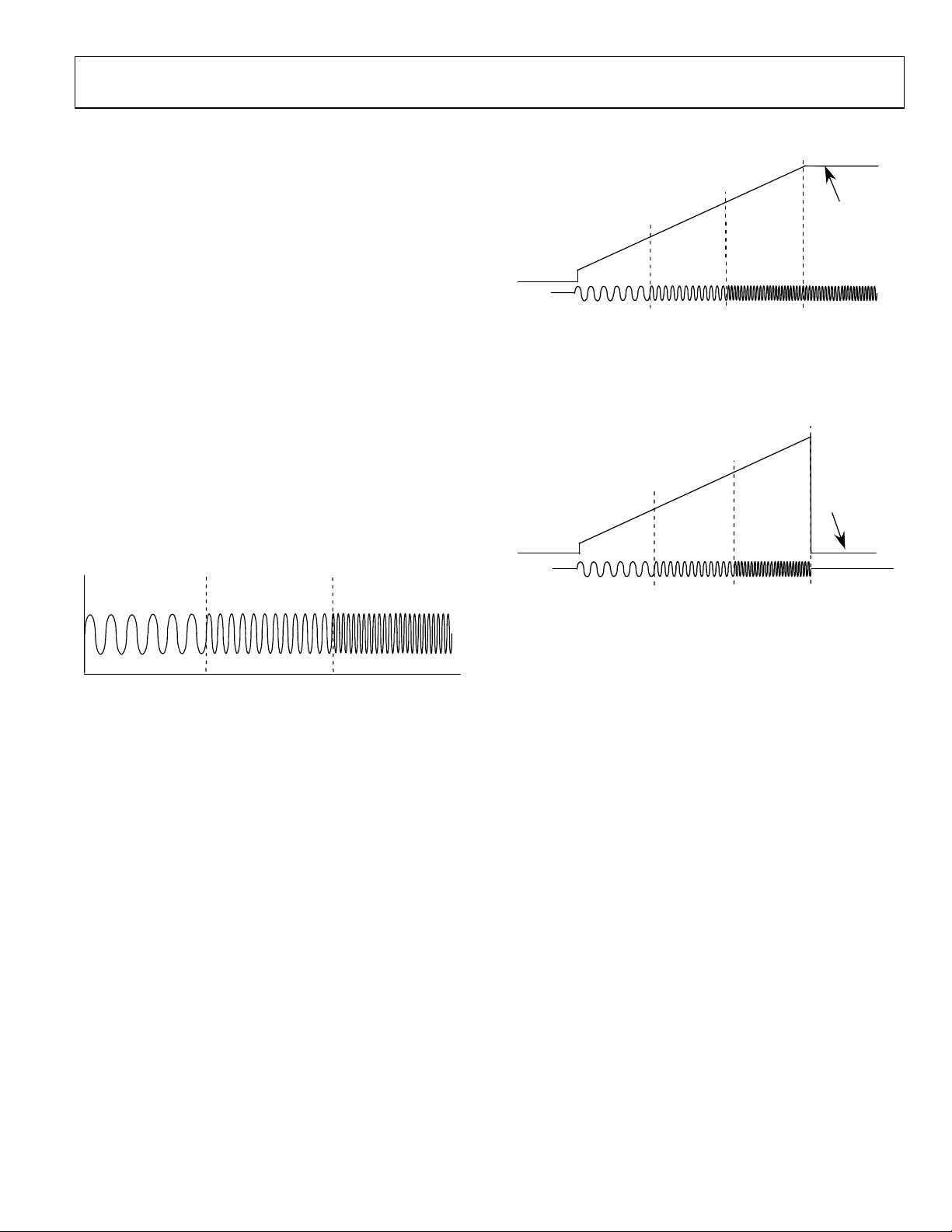
DETAILED OPERATION
The AD5932 is a General Purpose Synthesized Waveform
Generator capable of providing digitally programmable
+N
INCR
Final Frequency out
Midscale out
x ∆F
Waveform Sequences in both the frequency and time domain.
The device contains embedded digital processing to provide a
scan of a user-programmable frequency profile allowing
enhanced frequency control. Because the device is preprogrammable, it eliminates continuous write cycles from a
DSP/microcontroller in generating a particular waveform.
The frequency profile is defined by a Start Frequency (F
START
), a
Frequency Increment (Δf) and the number of increments per
Scan (N
increments, (t
). The Increment interval between frequency
INCR
), is either user-programmable and frequency
INT
automatically incremented by the device or externally
controlled via a hardware pin. For automatic update the interval
profile can either be for a fixed number of clock periods or for a
fixed number of output waveform cycles. An example of a 3step frequency scan is shown in Figure 3. Note the frequency
swept output signal is continuously available, and is therefore
phase continuous at all frequency increments.
F
START
Midscale
Figure 4. Frequen cy scan, Final f requency out
For the second option, the A5932 comDpletes the scan as before,
but in this case it outputs Miscale at the end of the scan. As before,
the frequency scan time is
5.
F
START
Midscale
Figure 5. Frequency scan, Midscale out
(N
F
INCR
START
+ 1) x T
+ ∆FF
. This is shown in Figure
INT
START
1
Number Steps Changes
Figure 3. Operation of the AD5932
2
In the auto-increment mode, a single pulse at the CTRL pin
starts and executes the frequency scan. In the externalincrement mode the CTRL pin also starts the scan but the
frequency increment interval is determined by the time interval
between sequential 0 /1 transitions on the CTRL pin.
The user has the option of two outputs once the frequency scan
is complete:
Output the last frequency in the scan or
reset and output midscale.
For the first option, the AD5932 completes the frequency scan
from frequency-start to frequency-end, i.e. from F
+ N
incrementally to (F
START
× Δf), and then continues to
INCR
START
output the last frequency is the scan. This is shown in Figure 4.
This gives a frequency scan time of (N
INCR
+ 1) x T
INT
.
The AD5932 offers two digital outputs, available from the MSB
OUT pin and the SYNC O/P pin. The inverted MSB of the DAC
data is available at the MSB OUT pin. The SYNC O/P can be
used to give the status of the scan. It is user selectable for the
End of the Scan, or to output a 4 × T
pulse at frequency
CLOCK
increments.
FUNCTIONAL DESCRIPTION
Serial Interface
The AD5932 has a standard 3-wire serial interface, which is
compatible with SPI, QSPI, MICROWIRE and DSP interface
standards.
Data is loaded into the device as a 16-bit word under the control
of a serial clock input, SCLK. The timing diagram for this
operation is given in Figure .
The FSYNC input is a level triggered input that acts as a frame
synchronization and chip enable. Data can only be transferred
into the device when FSYNC is low. To start the serial data
transfer, FSYNC should be taken low, observing the minimum
FSYNC to SCLK falling edge setup time, t
low, serial data will be shifted into the device's input shift
register on the falling edges of SCLK for 16 clock pulses. FSYNC
may be taken high after the sixteenth falling edge of SCLK,
observing the minimum SCLK falling edge to FSYNC rising
edge time, t
.Alternatively, FSYNC can be kept low for a
8
multiple of 16 SCLK pulses, and then brought high at the end of
. After FSYNC goes
7
Rev. PrA | Page 9 of 15

AD5932 Preliminary Technical Data
the data transfer. In this way, a continuous stream of 16 bit
words can be loaded while FSYNC is held low, FSYNC only
going high after the 16th SCLK falling edge of the last word
loaded.
The SCLK can be continuous or, alternatively, the SCLK can idle
high or low between write operations.
Powering Up the AD5932
When the AD5932 is powered up, the part is in an un-defined
state, and therefore must be reset before use. The 7 registers
(control and frequency) will contain invalid data and, therefore,
should all be set to a known value by the user. The control
register should be the first register to be programmed, as this
sets up the part. Note that a write to the control register will
automatically reset the internal state machines, and will provide
an analog output of midscale as it provides the same function as
the INTERRUPT pin. Typically, this is followed by a serial
loading of all the required scan parameters. The DAC output
remains at midscale until a scan is started using the CTRL pin.
OUTPUTS FROM THE AD5932
The AD5932 offers a variety of outputs from the chip. The
analog outputs are available from the V
sinewave and a triangle output. The square-wave output is
available from the MSB OUT pin.
Sinusoidal Output: The SIN ROM is used to convert the phase
information from the frequency and phase registers into
amplitude information, which results in a sinusoidal signal at
the output. To have a sinusoidal output from the V
the bit SINE/TRI (D9) in the control register to 1.
Triangle O u t p u t : The SIN ROM can be bypassed so that the
truncated digital output from the NCO is sent to the DAC. In
this case, the output is no longer sinusoidal. The DAC produces
10-bit linear triangular function. To have a triangle output from
the V
pin, set the bit SINE/TRI (D9) = 0.
OUT
Note that the DAC ENABLE bit (D10) must be “1” (i.e. the DAC
is enabled) when using these pins.
Digital Outputs: The digital outputs are available from the
MSB OUT pin and the SYNCOP pin. The inverse of the MSB of
the DAC data is available at the MSB OUT pin. The MSB OUT
pin must be enabled before use. The enabling/disabling of this
pin is controlled by the bit MSBOUTEN (D8) in the control
pin, and include a
OUT
OUT
pin, set
register. When MSBOUTEN = 1, this pin is enabled. This is
useful as a synthesised clock source.
PROGRAMMING THE AD5932
The AD5932 is designed to provide automatic frequency scans
when the CTRL pin is triggered. The automatic scan is
controlled by a set of registers, the addresses of which are given
in the table below. The function of each register is described in
the subsequent pages.
Table 4. Regsister Adresseses
Register Address
D15 D14 D13 D12 Mnemonic Name
0 0 0 0 C
0 0 0 1 N
0 0 1 0
0 0 1 1
0 1 T
1 0 x x Reserved
1 1 0 0 F
1 1 0 1 F
1 1 1 0 Reserved
1 1 1 1 Reserved
The Control Register
The AD5932 contains a 12-bit control register which sets up the
operating modes of the AD5932. The different functions and
the various output options from the AD5932 are controlled by
this register. Table 5 below describes the individual bits of the
control register.
To address the control register, D15 to D12 of the 16-bit serial
word must be set to '0' .
Table 5.Control Register
D15 D14 D13 D12 D11 D0
0 0 0 0 CONTROL BITS
Control Bits
REG
INCR
∆f
∆f
Increment Interval
INT
START
START
Number of
Increments
Lower 12 bits of
Delta Frequency
Higher 12 bits of
Delta Frequency
Lower 12 bits of
Start Frequency
Higher 12 bits of
Start Frequency
Rev. PrA | Page 10 of 15

Preliminary Technical Data AD5932
Table 6. Description of bits in the Control Register
Bit Name Function
D15–
D12
D11 B24 Two write operations are required to load a complete word into the F
D10 DAC ENABLE
D9 SINE/TRI
D8 MSBOUTEN When MSBOUTEN = '1', the MSBOUT pin is enabled.
D7 Reserved This bit must always be set to 1.
D6 Reserved This bit must always be set to 1.
D5 INT/EX INCR When INT/EX INCR = '1' the frequency increments are triggered externally through the CTRL pin.
D4 MODE The function of this bit is to control what the AD5932 will output at the end of the frequency scan.
D3 SYNCSEL User selectable for “End of Scan” (EOS), or Frequency Increments
D2 SYNCOUTEN When SYNCOUTEN= '1', the SYNC output is available at the pin SYNCOP.
D1 Reserved This bit must always be set to 1.
D0 Reserved This bit must always be set to 1.
ADDR Register Address bits.
B24 = '1' allows a complete word to be loaded into a frequency register in two consecutive writes. The first write
contains the 12 LSBs of the frequency word and the next write will contain the 12 MSBs. Refer to Table 4 for the
appropriate addresses. The write to the destination register occurs after both words have been loaded, so the
register never holds an intermediate value.
When B24 = '0' the 24-bit F
other containing the 12 LSBs. This means that the 12 MSBs of the frequency word can be altered independent of
the 12 LSBs and vice versa. This is useful if the complete 24 bit update is not required. To alter the 12 MSBs or the
12 LSBs, a single write is made to the appropriate register address. Refer to Table 4 for the appropriate addresses.
When DAC ENABLE = '1', the DAC is enabled.
When DAC ENABLE = '0', the DAC is powered down. This is useful if a user is just using the MSB of the DAC data
(available at the MSBOUT pin), and wants to save power.
The function of this bit is to control what is available at the V
When SINE/TRI = '1' the SIN ROM is used to convert the phase information into amplitude information which
results in a sinusoidal signal at the output (See Table 4).
When SINE/TRI = '0', the SIN ROM is bypassed, resulting in a triangular (up-down) output from the DAC.
When MSBOUTEN = '0', the MSBOUT is disabled (tri-state).
When INT/EX INCR = '0', the frequency increments are triggered automatically.
When MODE = '1', the devcie outputs the last frequency in the scan.
When MODE = '0', the AD5932 resets and outputs miscale.
When SYNCSEL = '1', the SYNCOP pin outputs a high level the End of the scan and returns to zero at the start of a
new frequency scan.
When SYNCSEL= '0', the SYNCOP outputs a pulse of 4 × T
When SYNCOUTEN= '0', the SYNCOP pin is disabled (tri-state).
register and the ∆f register.
START
/∆f register operates as 2 12-bit registers, one containing the 12 MSBs and the
START
pin.
OUT
only at each frequency increment.
CLOCK
Rev. PrA | Page 11 of 15

AD5932 Preliminary Technical Data
SETTING UP THE FREQUENCY SCAN
As stated previously, the AD5932 requires certain registers to be
programmed to enable a frequency scan. The frequency profile
is described by data for the Start Frequency (F
Frequency Increment ( Δf) and for the number of increments
per Scan (N
). The Increment interval (T
INCR
frequency increments during the scan is user-programmable,
and can either be for a fixed number of clock periods or for a
fixed number of output waveform cycles. The following section
discusses these registers in more detail.
Start Frequency (F
START
)
To start a frequency scan, the user needs to tell the AD5932
what frequency to start scanning from. This frequency is stored
in a 24-bit register called F
entire contents of the F
. If the user wishes to alter the
START
register, two consecutive writes
START
must be preformed, one to the LSBs and the other to the MSBs.
Note that for an entire write to this register, the control bit B24
(D11) should be set to ‘1’. With the LSBs programmed first.
Table 7. F
Register Bits
START
D15 D14 D13 D12 D11 D0
1 1 0 0 12 LSBs of F
1 1 0 1 12 MSBs of F
In some applications, the user does not need to alter all 24 bits
of the F
register. By setting the control bit B24 (D11) to ‘0’,
START
the 24-bit register operates as two 12-bit registers, one
containing the 12 MSBs and the other containing the 12 LSBs.
This means that the 12MSBs of the F
word can be altered
START
independently of the 12 LSBs, and vice versa. The addresses of
both the LSBs and the MSBs of this register is given in Table 7.
Frequency Increments (∆f)
The value in the Δf register sets the Increment frequency for the
scan and is added incrementally to the current frequency being
output. Note that the increment frequency can be positive or
negative, thereby giving an increasing or decreasing frequency
scan.
At the start of a scan, the frequency contained in the F
register wil l be output. Next, t he frequency (F
output. This will be followed by (F
+ Δ f + Δf) and so on.
START
Multiplying the Δf value by the number of Increments (N
and adding it to the start frequency (F
), will give the final
START
frequency in the scan. Mathematically this final frequency/stop
frequency is represented by F
START
+ (N
× Δ f). The Δf
INCR
register is a 23-bit register, and requires two 16-bit writes to be
programmed. Table 8 gives the addresses associated with both
the MSB and LSB registers of the Δf word.
START
) between
INT
START
START
+ Δ f ) will be
START
), the
<11….0>
<23….12>
START
INCR
),
D15 D14 D13 D12 D11 D10 D0
0 0 1 0
0 0 1 1 0
0 0 1 1 1
Number of Increments (N
An End frequency is not required on the AD5932. Instead, this
End frequency is calculated by multiplying the frequency
Increment value (Δf) value by the number of Frequency Steps
), and adding it to/subtracting it from the start frequency
(N
INCR
)., i.e. F
(F
START
The N
register is a 12 bit register, with the address shown in
INCR
the table below.
D15 D14 D13 D12 D11 D0
0 0 0 1 12 bits of N
The number of increments is programmed in binary fashion,
with 000000000010 representing the minimum number of
frequency increments (2 increments), and 111111111111
representing the maximum number of increments (4095).
D11 D0 No. of Increments
0000 0000 0010
0000 0000 0011 3 frequency increments.
0000 0000 0100 4 frequency increments.
. . . . . .
1111 1111 1110 4094 frequency increments.
1111 1111 1111 4095 frequency increments.
Increment Interval (T
The increment interval dictates the duration for which the DAC
output signal for each individual frequency of the Frequency
scan will be available. The AD5932 offers the user two choices:
• To have the duration as a multiple of cycles of the output
frequency.
Table 8. ∆f Register Bits
12 LSBs of Δf
<11….0>
INCR
START
+ (N
Table 9. N
INCR
× Δ f).
INCR
Table 10. N
2 frequency increments. This is a
minimum number of Frequency
Increments
)
INT
11 MSBs of
Δf
<22….12>
11 MSBs of
Δf
<22….12>
)
Register Bits
Data Bits
INCR
Scan
Direction
n/a
Positive Δf
(F
+ Δf)
START
Negative ∆f
(F
- Δf)
START
<11….0>
INCR
• To have the duration as a multiple of MCLK periods.
This is selected by Bit D13 in the T
Table 11.
Rev. PrA | Page 12 of 15
register as shown in
INT

Preliminary Technical Data AD5932
Table 11. t
D15 D14 D13 D12 D11 D10 D0
0 1 0 x x 11 bits <10 …..0>
0 1 1 x x 11 bits <10 ….0>
Register Bits
INT
Fixed number of output
waveform cycles
Fixed number of clock
periods
Programming of this register is in binary form with the
minimum number being decimal 2. Note from the table above
that there are 11 bits, <D10 to D0>, of the register available to
program the time interval As an example, for MCLK = 50 MHz,
each clock period/base interval is (1/50 MHz) = 20 ns. If, for
example, each frequency needs to be output for 100ns, then
<00000000101> or decimal 5 needs to be programmed to this
register. Note that the AD5932 can output each frequency for a
11
maximum duration of 2
−1 (or 2047) times the increment
interval. So for the MCLK = 50MHz example, a time interval of
20 ns × 2047 = 40 µs is maximum, with the minimum being 40
ns.
In the example above, the maximum time that an individual
frequency can be output is 40 µs. For some applications, this
may be insufficient. Therefore to cater for scans that need a
longer Increment Interval, Time-base Multipliers are provided.
In
Table 11, D12 and D11 are dedicated to the Time-base
Multipliers. A more detailed table of the Multiplier options is
given in Table 12 below.
To explain this via an example, and again assuming an MCLK of
50 MHz. If a multiplier of 500 is used, then the base interval is
now (1/(50 MHz) x 500)) = 10µs. Therefore, using a multiplier
11 − 1
of 500, the maximum Increment Interval is 10 µs × 2
=
20.5 ms. Therefore, as can be seen from the example above, the
option of Time-base Multipliers gives the user great flexibility
when programming the length of the frequency window as any
frequency can be output for a minimum of 40 ns up to a
maximum of 20.5 ms.
Table 12. Time-base Multiplier Values
D12 D11 Multiplier value
0 0 Multiply (1/MCLK) by 1
0 1 Multiply (1/MCLK) by 5
1 0 Multiply (1/MCLK) by 100
1 1 Multiply (1/MCLK) by 500
Length of Scan Time
The length of time to complete a user-programmed frequency
scan is given by the following equation:
T
SCAN
= (1 + N
INCR
) × T
INT
Rev. PrA | Page 13 of 15

AD5932 Preliminary Technical Data
OUTLINE DIMENSIONS
0.201 (5.10)
0.193 (4.90)
16 9
)
)
0
0
3
5
.
.
4
4
(
(
9
7
6
7
1
1
.
.
0
0
1
PIN
0.0256
(0.65)
BSC
1
0.0118 (0.30)
0.0075 (0.19)
0.006 (0.15)
0.002 (0.05)
SEATING
PLANE
Figure 3. 16-Lead Small Outline Package (TSSOP)
Dimensions shown in millimeters
ORDERING GUIDE
Model Temperature Range Package Description Package Option
AD5932YRUZ −40 °C to +105 °C 16-lead TSSOP (Thin Shrink Small Outline Package) RU-16
AD5932YRUZ-REEL −40 °C to +105 °C 16-lead TSSOP (Thin Shrink Small Outline Package) RU-16
8
(RU-16)
)
)
5
0
2
5
.
.
6
6
(
(
6
6
4
5
2
2
.
.
0
0
0.0433
(1.10)
MAX
0.0079 (0.20)
0.0035 (0.090)
8°
0°
0.028 (0.70)
0.020 (0.50)
Rev. PrA | Page 14 of 15

Preliminary Technical Data AD5932
© 2005 Analog Devices, Inc. All rights reserved. Trademarks and
registered trademarks are the property of their respective owners.
PR05416–0–2/05(PrA)
Rev. PrA | Page 15 of 15
 Loading...