现货库存、技术资料、百科信息、热点资讯,精彩尽在鼎好!
Programmable Frequency Sweep and
FEATURES
Programmable frequency profile
No external components necessary
Output frequency up to 25 MHz
Burst and listen capability
Preprogrammable frequency profile minimizes number of
DSP/µcontroller writes
Sinusoidal/triangular/square wave outputs
Automatic or single pin control of frequency stepping
Waveform starts at known phase
Increments at 0° phase or phase continuously
Power-down mode: 20 µA
Power supply: 2.3 V to 5.5 V
Automotive temperature range: −40°C to +125°C
20-lead pb-free TSSOP
APPLICATIONS
Frequency sweeping/radar
Network/impedance measurements
Incremental frequency stimulus
Sensory applications
Proximity and motion
BFSK
Frequency bursting/pulse trains
Output Burst Waveform Generator
AD5930
GENERAL DESCRIPTION
The AD59301 is a waveform generator with programmable
frequency sweep and output burst capability. Utilizing
embedded digital processing that allows enhanced frequency
control, the device generates synthesized analog or digital
frequency-stepped waveforms. Because frequency profiles
are preprogrammed, continuous write cycles are eliminated
and thereby free up valuable DSP/µcontroller resources.
Waveforms start from a known phase and are incremented
phase continuously, which allows phase shifts to be easily
determined. Consuming only 8 mA, the AD5930 provides a
convenient low power solution to waveform generation.
The AD5930 can be operated in a variety of modes. In
continuous output mode, the device outputs the required
frequency for a defined length of time and then steps to the
next frequency. The length of time the device outputs a
particular frequency is either preprogrammed and the device
increments the frequency automatically, or, alternatively, is
incremented externally via the CTRL pin. In burst mode, the
device outputs its frequency for a length of time and then
returns to midscale for a further predefined length of time
before stepping to the next frequency. When the MSBOUT pin
is enabled, a digital output is generated.
(continued on Page 3)
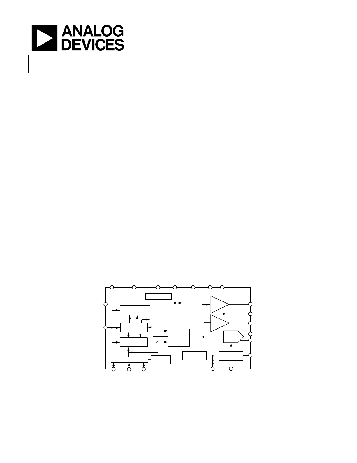
FUNCTIONAL BLOCK DIAGRAM
INTERRUPT
MCLK
CTRL
1
Protected by US Patent Number 6747583, other patents pending.
Rev. 0
Information furnished by Analog Devices is believed to be accurate and reliable. However, no
responsibility is assumed by Anal og Devices for its use, nor for any infringements of patents or other
rights of third parties that may result from its use. Specifications subject to change without notice.
No license is granted by implication or otherwise under any patent or patent rights of Analog
Devices. Trademarks and registered trademarks are the property of their respective owners.
STANDBY DVDD CAP/2.5V DGND AGND AVDD
AD5930
OUTPUT BURST
CONTRO LLER
DATA
INCREMENT
CONTROLL ER
DATA
FREQUENCY
CONTRO LLER
DATA
SERIAL INTERFACE
FSYNC SCLK SDATA
REGULATOR
SYNC
INCR
AND CONTROL
CONTRO L
REGISTER
24
PIPELINED
DDS CORE
24-BIT
Figure 1.
VCC
SYNC
2.5V
ON-BOARD
REFERENCE
One Technology Way, P.O. Box 9106, Norwood, MA 02062-9106, U.S.A.
Tel: 781.329.4700
Fax: 781.461.3113 © 2005 Analog Devices, Inc. All rights reserved.
BUFFER
BUFFER
10-BIT
DAC
FULL-SCALE
CONTROL
REF FSADJUST
SYNCOUT
DGND O/P
MSBOUT
IOUTB
IOUT
COMP
05333-001
www.analog.com

AD5930
TABLE OF CONTENTS
Features .............................................................................................. 1
Powering up the AD5930 .......................................................... 17
Applications....................................................................................... 1
General Description......................................................................... 1
Functional Block Diagram .............................................................. 1
Revision History ............................................................................... 2
Specifications..................................................................................... 4
Timing Characteristics..................................................................... 6
Absolute Maximum Ratings............................................................ 8
ESD Caution.................................................................................. 8
Pin Configuration and Function Descriptions............................. 9
Typical Performance Characteristics ........................................... 11
Te r mi n ol o g y .................................................................................... 15
Theory of Operation ...................................................................... 16
The Frequency Profile................................................................ 16
Output Modes............................................................................. 16
Serial Interface............................................................................ 17
Programming the AD5930........................................................ 17
Setting up the Frequency Sweep............................................... 19
Activating and Controlling the Sweep..................................... 20
Outputs from the AD5930........................................................ 21
Applications..................................................................................... 22
Grounding and Layout .............................................................. 22
AD5930 to ADSP-21xx Interface ............................................. 22
AD5930 to 68HC11/68L11 Interface....................................... 23
AD5930 to 80C51/80L51 Interface.......................................... 23
AD5930 to DSP56002 Interface ............................................... 23
Evaluation Board ........................................................................ 24
Schematic..................................................................................... 25
Outline Dimensions ....................................................................... 27
Ordering Guide .......................................................................... 27
REVISION HISTORY
11/05—Revision 0: Initial Version
Rev. 0 | Page 2 of 28

AD5930
GENERAL DESCRIPTION
(continued from Page 1)
To program the device, the user enters the start frequency, the
increment step size, the number of increments to be made, and
the time interval that the part outputs each frequency. The
frequency sweep profile is initiated, started, and executed by
toggling the CTRL pin.
A number of different sweep profiles are offered. Frequencies can
be stepped in triangular-sweep mode, which continuously sweeps
up and down through the frequency range. Alternatively, in sawsweep mode, the frequency is swept up through the frequency
range, but returns to the initial frequency before executing the
sweep again. In addition, a single frequency or burst can be
generated without any sweep.
The AD5930 is written to via a 3-wire serial interface, which
operates at clock rates up to 40 MHz. The device operates with
a power supply from 2.3 V to 5.5 V. Note that AV
are independent of each other and can be operated from
different voltages. The AD5930 also has a standby function,
which allows sections of the device that are not being used
to be powered down.
The AD5930 is available in a 20-lead pb-free TSSOP package.
and DVDD
DD
Rev. 0 | Page 3 of 28

AD5930
SPECIFICATIONS
AVDD = DVDD = 2.3 V to 5.5 V, AGND = DGND = 0 V, TA = T
unless otherwise noted.
Table 1.
Y Grade
1
Parameter Min Typ Max Unit Test Conditions/Comments
SIGNAL DAC SPECIFICATIONS
Resolution 10 Bits
Update Rate 50 MSPS
I
Full-Scale
OUT
V
Peak-to-Peak 0.56 V
OUT
V
Offset 45 mV From 0 V to the trough of the waveform
OUT
V
MIDSCALE
2
3 4.0 mA
0.325 V Voltage at midscale output
Output Compliance 0.8 V AV
DC Accuracy
Integral Nonlinearity (INL) ±1.5 LSB
Differential Nonlinearity (DNL) ±0.75 LSB
DDS SPECIFICATIONS
Dynamic Specifications
Signal-to-Noise Ratio 53 60 dB f
Total Harmonic Distortion −60 −53 dBc f
Spurious-Free Dynamic Range
(SFDR)
Wideband (0 to Nyquist) −62 −52 dBc f
Narrowband (±200 kHz) −76 −73 dBc f
Clock Feedthrough −50 dBc Up to 16 MHz out
Wake-Up Time 1.7 ms From standby
OUTPUT BUFFER
V
Peak-to-Peak 0 DVDDV Typically, square wave on MSBOUT and SYNCOUT
OUT
Output Rise/Fall Time
2
12 ns
VOLTAGE REFERENCE
Internal Reference 1.15 1.18 1.26 V
External Reference Range 1.3 V
REFOUT Input Impedance 1 kΩ VIN @ REF pin < Internal V
25 kΩ VIN @ REF pin > Internal V
Reference TC
2
90 ppm/°C
LOGIC INPUTS
Input Current 0.1 ±1 µA
V
, Input High Voltage 1.7 V DVDD = 2.3 V to 2.7 V
INH
2.0 V DVDD = 2.7 V to 3.6 V
2.8 V DVDD = 4.5 V to 5.5 V
V
, Input Low Voltage 0.6 V DVDD = 2.3 V to 2.7 V
INL
0.7 V DVDD = 2.7 V to 3.6 V
0.8 V DVDD = 4.5 V to 5.5 V
CIN, Input Capacitance
LOGIC OUTPUTS
2
2
3 pF
VOH, Output High Voltage DVDD − 0.4 V V I
VOL, Output Low Voltage 0.4 V I
Floating-State O/P Capacitance 5 pF
MIN
to T
MAX
, R
= 6.8 kΩ, R
SET
= 2.3 V, internal reference used
DD
= 50 MHz, f
MCLK
= 50 MHz, f
MCLK
= 50 MHz, f
MCLK
= 50 MHz, f
MCLK
= 1 mA
SINK
= 1 mA
SINK
= 200 Ω for IOUT and IOUTB,
LOAD
OUT
OUT
OUT
OUT
= f
= f
= f
= f
MCLK
MCLK
MCLK
MCLK
3
/4096
/4096
/50
/50
REF
REF
Rev. 0 | Page 4 of 28
AD5930
F
Y Grade
1
Parameter Min Typ Max Unit Test Conditions/Comments
POWER REQUIREMENTS f
AVDD/DV
I
AA
I
DD
IAA + I
DD
DD
2.3 5.5 V
3.8 4 mA
2.4 2.7 mA
6.2 6.7 mA
= 50 MHz, f
MCLK
OUT
= f
MCLK
/7
Low Power Sleep Mode Device is reset before putting into standby
20 85 µA All outputs powered down, MCLK = 0 V, serial interface active
140 240 µA All outputs powered down, MCLK active, serial interface active
1
Operating temperature range is as follows: Y Version: −40°C to +125°C; typical specifications are at 25°C.
2
Guaranteed by design.
3
Minimum R
= 3.9 kΩ.
SET
R
SET
FSADJUST
CONTROL
6.8V
COMP
AVD D
10nF
100n
10nF
CAP/2.5V
REGULATOR
REFOUT
ON-BOARD
REFERENCE
FULL-SCALE
AD5930
12
SIN
ROM
10-BIT
DAC
IOUT
R
LOAD
200V
20pF
05333-002
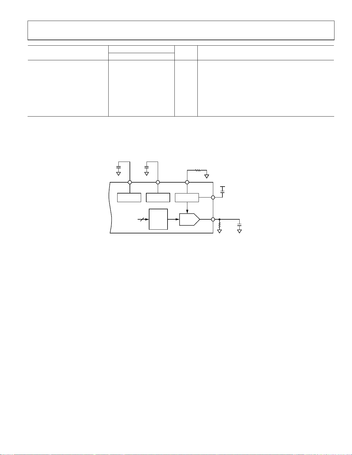
Figure 2. Test Circuit Used to Test the Specifications
Rev. 0 | Page 5 of 28
AD5930
C
TIMING CHARACTERISTICS
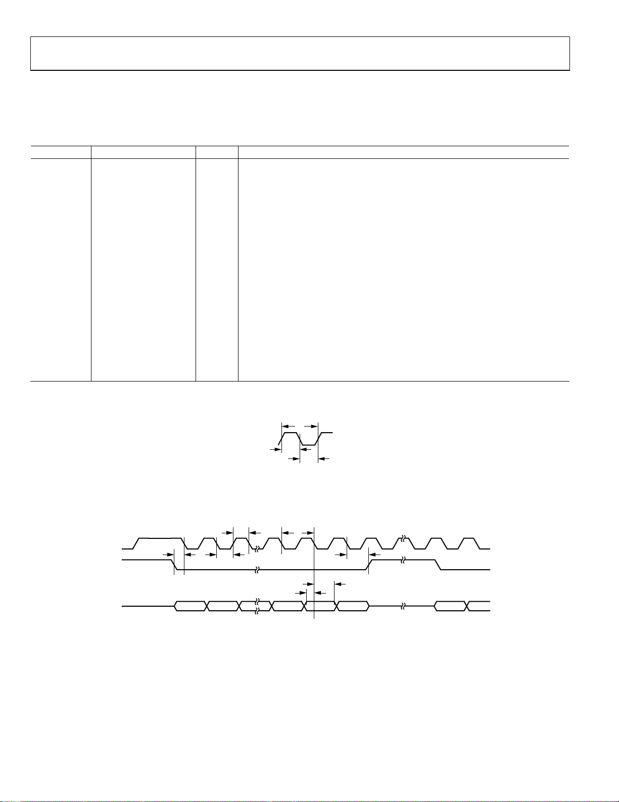
All input signals are specified with tr = tf = 5 ns (10% to 90% of VDD) and timed from a voltage level of (VIL + VIH)/2.
See Figure 4 to Figure 7. DV
1
Table 2.
Parameter Limit at T
t
1
t
2
t
3
t
4
t
5
t
6
t
7
t
8
t
9
t
10
t
11
t
12
t
13
8 x t
t
14
t
15
t
16
t
17
1
Guaranteed by design, not production tested.
20 ns min MCLK period
8 ns min MCLK high duration
8 ns min MCLK low duration
25 ns min SCLK period
10 ns min SCLK high time
10 ns min SCLK low time
5 ns min FSYNC to SCLK falling edge setup time
10 ns min FSYNC to SCLK hold time
5 ns min Data setup time
3 ns min Data hold time
2 x t
1
0 ns min CTRL rising edge to MCLK falling edge setup time
10 x t
1
1
2 x t
1
2 x t
1
2 x t
1
20 ns max MCLK falling edge after 16th clock edge to MSB out
= 2.3 V to 5.5 V, AGND = DGND = 0 V, all specifications T
DD
, T
MIN
MAX
Unit Conditions/Comments
ns min Minimum CTRL pulse width
ns typ CTRL rising edge to IOUT/IOUTB delay (initial pulse, includes initialization)
ns typ CTRL rising edge to IOUT/IOUTB delay (initial pulse, includes initialization)
ns typ Frequency change to SYNC output, saw sweep, each frequency increment
ns typ Frequency change to SYNC output, saw sweep, end of sweep
ns typ Frequency change to SYNC output, triangle sweep, end of sweep
t
MCLK
Figure 3. Master Clock
1
t
2
t
3
05333-003
MIN
to T
, unless otherwise noted.
MAX
SCLK
FSYN
SDATA
t
5
t
7
D15 D14 D2 D1 D0 D15 D14
t
6
Figure 4. Serial Timing
t
4
t
8
t
10
t
9
05333-004
Rev. 0 | Page 6 of 28
AD5930
y
y
t
MCLK
12
CTRL
IOUT/IOUTB
t
11
t
13
05333-005
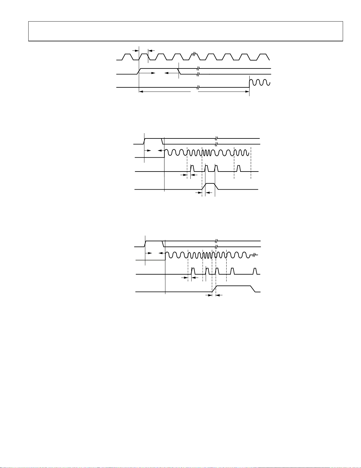
Figure 5. CTRL Timing
CTRL
t
13
IOUT
SYNC O/P
(Each Frequenc
Increment )
SYNC O/P
(End of Sweep)
t
14
t
15
05333-006
Figure 6. CTRL Timing, Saw-Sweep Mode
CTRL
IOUT
SYNC O/P
(Each Frequenc
Increment )
SYNC O/P
(End of Sweep)
t
13
t
14
t
16
Figure 7. CTRL Timing, Triangular-Sweep Mode
05333-007
Rev. 0 | Page 7 of 28

AD5930
ABSOLUTE MAXIMUM RATINGS
TA = 25°C, unless otherwise noted.
Table 3.
Parameter Rating
AVD D to AGND −0.3 V to +6.0 V
DVDD to DGND −0.3 V to +6.0 V
AGND to DGND −0.3 V to +0.3 V
CAP/2.5V to DGND −0.3 V to 2.75 V
Digital I/O Voltage to DGND −0.3 V to DVDD + 0.3 V
Analog I/O Voltage to AGND −0.3 V to AVDD + 0.3 V
Operating Temperature Range
Automotive (Y Version) −40°C to +125°C
Storage Temperature Range −65°C to +150°C
Maximum Junction Temperature +150°C
TSSOP Package (4-Layer Board)
θJA Thermal Impedance 112°C/W
θJC Thermal Impedance 27.6°C/W
Reflow Soldering (Pb-Free) 300°C
Peak Temperature 260(+0/−5)°C
Time at Peak Temperature 10 sec to 40 sec
Stresses above those listed under Absolute Maximum Ratings
may cause permanent damage to the device. This is a stress
rating only; functional operation of the device at these or any
other conditions above those indicated in the operational
section of this specification is not implied. Exposure to absolute
maximum rating conditions for extended periods may affect
device reliability.
ESD CAUTION
ESD (electrostatic discharge) sensitive device. Electrostatic charges as high as 4000 V readily accumulate on the
human body and test equipment and can discharge without detection. Although this product features
proprietary ESD protection circuitry, permanent damage may occur on devices subjected to high energy
electrostatic discharges. Therefore, proper ESD precautions are recommended to avoid performance
degradation or loss of functionality.
Rev. 0 | Page 8 of 28
AD5930
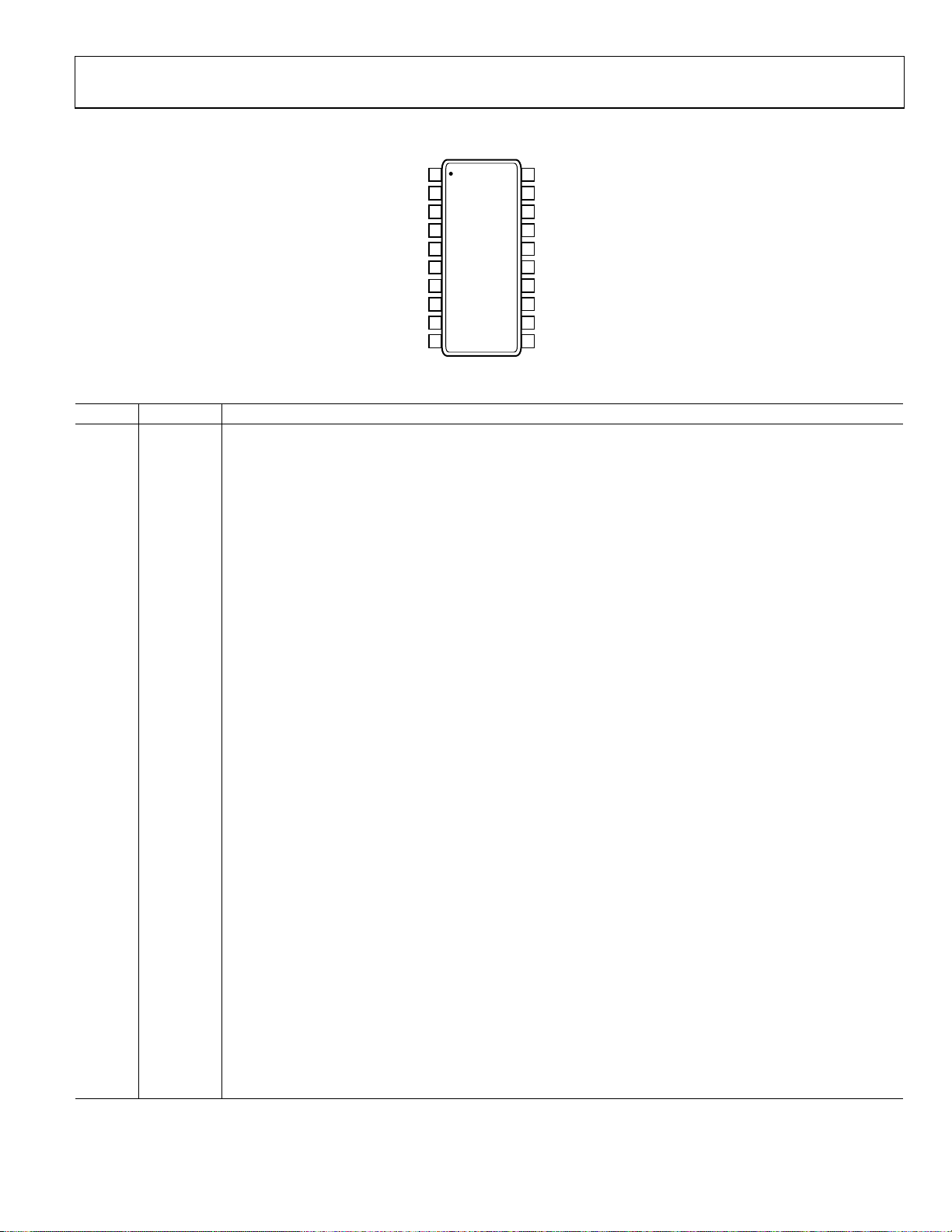
PIN CONFIGURATION AND FUNCTION DESCRIPTIONS
FSADJUST
REF
COMP
AVD D
DVDD
CAP/2.5V
DGND
MCLK
SYNCOUT
MSBOUT
1
2
3
4
(Not to S cale)
5
6
7
8
9
10
AD5930
TOP VIEW
20
IOUTB
19
IOUT
18
AGND
17
STANDBY
16
FSYNC
15
SCLK
14
SDATA
13
CTRL
12
INTERRUPT
11
DGND O/P
05333-008
Figure 8. Pin Configuration
Table 4. Pin Function Descriptions
Pin No. Mnemonic Description
1 FSADJUST
Full-Scale Adjust Control. A resistor (RSET) must be connected externally between this pin and AGND.
This determines the magnitude of the full-scale DAC current. The relationship between R
full-scale current is:
2 REF
IOUT
where V
Voltage Reference. This pin can be an input or an output. The AD5930 has an internal 1.18 V reference, which
= 18 × V
FULL-SCALE
= 1.20 V nominal and R
REFOUT
REFOUT/RSET
= 6.8 kΩ typical.
SET
is made available at this pin. Alternatively, this reference can be overdriven by an external reference, with a
voltage range as given in the Specifications section. A 10 nF decoupling capacitor should be connected
between REF and AGND.
3 COMP DAC Bias Pin. This pin is used for decoupling the DAC bias voltage to AVDD.
4 AVDD
Positive Power Supply for the Analog Section. AVDD can have a value from +2.3 V to +5.5 V. A 0.1 µF decoupling
capacitor should be connected between AVDD and AGND.
5 DVDD
Positive Power Supply for the Digital Section. DVDD can have a value from +2.3 V to +5.5 V. A 0.1 µF decoupling
capacitor should be connected between DVDD and DGND.
6 CAP/2.5V
Digital Circuitry. Operates from a 2.5 V power supply. This 2.5 V is generated from DVDD using an on-board
regulator. The regulator requires a decoupling capacitor of typically 100 nF, which is connected from CAP/2.5V
to DGND. If DVDD is equal to or less than 2.7 V, CAP/2.5V can be shorted to DVDD.
7 DGND Ground for all Digital Circuitry. This excludes digital output buffers.
8 MCLK
Digital Clock Input. DDS output frequencies are expressed as a binary fraction of the frequency of MCLK.
The output frequency accuracy and phase noise are determined by this clock.
9 SYNCOUT
Digital Output for Sweep Status Information. User selectable for end of sweep (EOS) or frequency increments
through the control register (SYNCOP bit). This pin must be enabled by setting Control Register Bit SYNCOPEN to 1.
10 MSBOUT
Digital Output. The inverted MSB of the DAC data is available at this pin. This output pin must be enabled by
setting bit MSBOUTEN in the control register to 1.
11 DGND O/P Separate DGND Connection for Digital Output Buffers. Connect to DGND.
12 INTERRUPT
Digital Input. This pins acts as an interrupt during a frequency sweep. A low to high transition is sampled by the
internal MCLK, which resets internal state machines. This results in the DAC output going to midscale.
13 CTRL
Digital Input. Triple function pin for initialization, start, and external frequency increments. A low-to-high transition,
sampled by the internal MCLK, is used to initialize and start internal state machines, which then execute the pre-
programmed frequency sweep sequence. When in auto-increment mode, a single pulse executes the entire sweep
sequence. When in external increment mode, each frequency increment is triggered by low-to-high transitions.
14 SDATA
Serial Data Input. The 16-bit serial data-word is applied to this input with the register address first followed by the
MSB to LSB of the data.
15 SCLK Serial Clock Input. Data is clocked into the AD5930 on each falling SCLK edge.
16 FSYNC
Active Low Control Input. This is the frame synchronization signal for the serial data. When FSYNC is taken low,
the internal logic is informed that a new word is being loaded into the device.
17 STANDBY
Active High Digital Input. When this pin is high, the internal MCLK is disabled, and the reference DAC and regulator
are powered down. For optimum power saving, it is recommended to reset the AD5930 before putting it into
standby, as this results in a shutdown current of typically 20 µA.
Rev. 0 | Page 9 of 28
and the
SET
 Loading...