High Voltage, Quad-Channel
A
V
V
FEATURES
Quad-channel high voltage DAC
12-bit resolution
Pin selectable 30 V or 60 V output range
Integrated precision reference
Low power serial interface with readback capability
Integrated temperature sensor alarm function
Power-on reset
Simultaneous updating via
Wide operating temperature: −40°C to +105°C
APPLICATIONS
Programmable voltage sources
High voltage LED drivers
Receiver bias in optical communications
SDI
SDO
SCLK
SYNC
LARM
LDAC
CLRR_SEL
INPUT
CONTROL
LOGIC
POWER-ON
RESET
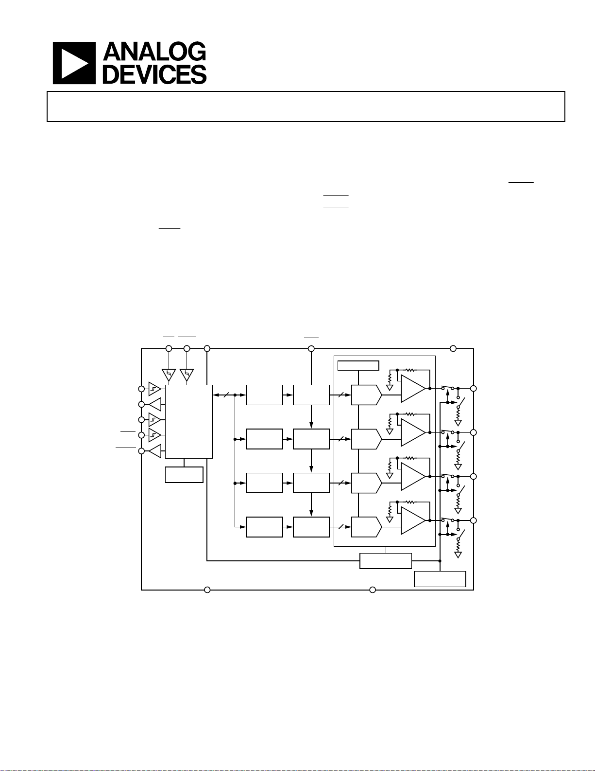
FUNCTIONAL BLOCK DIAGRAM
LOGIC
12
INPUT
REGISTER
A
INPUT
REGISTER
B
INPUT
REGISTER
C
INPUT
REGISTER
D
12-Bit Voltage Output DAC
GENERAL DESCRIPTION
The AD5504 is a quad-channel, 12-bit, serial input, digital-toanalog converter with on-chip high voltage output amplifiers
and an integrated precision reference. The DAC output voltage
ranges are programmable via the range select pin (
R_SEL
is held high, the DAC output ranges are 0 V to 30 V. If
R_SEL
is held low, the DAC output ranges are 0 V to 60 V. The
on-chip output amplifiers allow an output swing within the
range of AGND + 0.5 V to V
The AD5504 has a high speed serial interface, which is compatible with SPI®-, QSPI™-, MICROWIRE™-, and DSP-interface
standards and can handle clock speeds of up to 16.667 MHz.
LDAC
1713kΩ
–
+
1713kΩ
–
+
1713kΩ
–
+
1713kΩ
–
+
DAC
REGISTER
A
DAC
REGISTER
B
DAC
REGISTER
C
DAC
REGISTER
D
REFERENCE
122.36kΩ
DACA
12
122.36kΩ
DAC B
12
122.36kΩ
DAC C
12
122.36kΩ
DAC D
12
− 0.5 V.
DD
DD
V
OUTA
V
OUTB
V
OUTC
V
OUTD
AD5504
R_SEL
). If
AD5504
DGND AGND
POWER-DOWN
CONTROL LOGIC
TEMPERATURE
SENSOR
07994-001
Figure 1.
Rev. A
Information furnished by Analog Devices is believed to be accurate and reliable. However, no
responsibility is assumed by Analog Devices for its use, nor for any infringements of patents or other
rights of third parties that may result from its use. Specifications subject to change without notice. No
license is granted by implication or otherwise under any patent or patent rights of Analog Devices.
Trademarks and registered trademarks are the property of their respective owners.
One Technology Way, P.O. Box 9106, Norwood, MA 02062-9106, U.S.A.
Tel: 781.329.4700 www.analog.com
Fax: 781.461.3113 ©2009-2010 Analog Devices, Inc. All rights reserved.

AD5504
TABLE OF CONTENTS
Features .............................................................................................. 1
Applications ....................................................................................... 1
General Description ......................................................................... 1
Functional Block Diagram .............................................................. 1
Revision History ............................................................................... 2
Specifications ..................................................................................... 4
AC Characteristics ........................................................................ 5
Timing Characteristics ................................................................ 6
Absolute Maximum Ratings ............................................................ 8
Thermal Resistance ...................................................................... 8
ESD Caution .................................................................................. 8
Pin Configuration and Function Descriptions ............................. 9
Typical Performance Characteristics ........................................... 10
Terminology .................................................................................... 12
Theory of Operation ...................................................................... 14
Power-Up State ........................................................................... 14
Power-Down Mode .................................................................... 14
DAC Channel Architecture ....................................................... 14
Selecting the Output Range ...................................................... 14
CLR
Function.............................................................................. 14
LDAC
Function .......................................................................... 14
Temperature Sensor ................................................................... 15
Power Dissipation....................................................................... 15
Power Supply Sequencing ......................................................... 15
Serial Interface ................................................................................ 16
Write Mode ................................................................................. 16
Read Mode .................................................................................. 16
Writing to the Control Register ................................................ 16
Interfacing Examples ................................................................. 18
Outline Dimensions ....................................................................... 19
Ordering Guide .......................................................................... 19
REVISION HISTORY
10/10—Rev. 0 to Rev. A
Changes to Figure 3 and Figure 4 ................................................... 7
7/09—Revision 0: Initial Version
Rev. A | Page 2 of 20

AD5504
The serial interface offers the user the capability of both writing
to, and reading from, most of the internal registers. To reduce
power consumption at power up, only the digital section of the
AD5504 is powered up initially. This gives the user the ability to
program the DAC registers to the required value while typically
only consuming 30 A of supply current. The AD5504 incorporates power-on reset circuitry that ensures the DAC registers
power up in a known condition and remain there until a valid
write to the device has taken place. The analog section is
powered up by issuing a power-up command via the SPI
interface. The AD5504 provides software-selectable output
loads while in the power-down mode.
The AD5504 has an on-chip temperature sensor. When the
temperature on the die exceeds 110°C, the
active low CMOS output pin) flags an alarm and the AD5504
enters a temperature power-down mode disconnecting the
output amplifier thus removing the short-circuit condition. The
AD5504 remains in power-down mode until a software power-up
command is executed.
The AD5504 is available in a compact 16-lead TSSOP. The AD5504
is guaranteed to operate over the extended temperature range of
−40°C to +105°C.
Table 1. Related Device
Part No. Description
AD5501 High Voltage, 12-Bit Voltage Output DAC
ALARM
pin (an
Rev. A | Page 3 of 20

AD5504
SPECIFICATIONS
VDD = 10 V to 62 V; V
Table 2.
Parameter Symbol Min Typ1 Max Unit Test Conditions/Comments
ACCURACY
2
Resolution 12 Bits
Differential Nonlinearity DNL −1 1 LSB
Integral Nonlinearity INL
60 V Mode −2 +2 LSB VDD = 62 V
30 V Mode −3 +3 LSB VDD = 62 V
V
Temperature Coefficient
OUTX
Zero-Scale Error V
Zero-Scale Error Drift
Offset Error
6
Offset Error Drift
Full-Scale Error V
Full-Scale Error Drift
350 µV/°C +25°C to +105°C; 60 V mode
Gain Error −0.6 +0.6 % of FSR
Gain Temperature Coefficient
DC Crosstalk
4
R
Due to Single Channel Full-Scale
Output Change
Due to Powering Down (Per Channel) 4 mV 60 V mode
OUTPUT CHARACTERISTICS
Output Voltage Range
Short-Circuit Current
Capacitive Load Stability
RL = 60 kΩ to ∞ 1 nF
Load Current
4
−1 +1 mA On any single channel
DC Output Impedance
DC Output Leakage
DIGITAL INPUTS
Input Logic High VIH 2.0 V V
1.8 V V
Input Logic Low VIL 0.8 V V
Input Current IIL ±1 µA
Input Capacitance
DIGITAL OUTPUTS
Output High Voltage VOH V
Output Low Voltage VOL DGND + 0.4 V V I
Three-State Leakage Current
SDI, SDO, SCLK, LDAC, CLR, R_SEL
ALARM
Output Capacitance
POWER SUPPLIES
VDD 10 62 V
V
2.3 5.5 V
LOGI C
Quiescent Supply Current (I
Logic Supply Current (I
DC PSRR
4
DAC output = full-scale
60 V Mode 68 dB
= 2.3 V to 5.5 V; RL = 60 k; CL = 200 pF; −40°C < TA < +105°C, unless otherwise noted.
LOGIC
3, 4, 5
4
60 µV/°C 60 V mode
50 ppm/°C DAC code = half scale
100 mV DAC code = 0
ZSE
VOE −80 +120 mV
4
60 µV/°C 60 V mode
−325 +275 mV
4
1 mV/°C −40°C to +25°C; 60 V mode
4
10 ppm of FSR/°C 60 V mode
FSE
= 60 kΩ to AGND or VDD
L
3 mV 60 V mode
7
4, 8
2 mA On any single channel
4
1 V to 4 V step
4
3 Ω
4
10 µA
4
I
AGND + 0.5 VDD − 0.5 V
5 pF
IC
− 0.4 V V I
LOGI C
−1 +1 µA
= 4.5 V to 5.5 V
LOGI C
= 2.3 V to 3.6 V
LOGI C
= 2.3 V to 5.5 V
LOGI C
= 200 µA
SOURCE
= 200 µA
SINK
−10 +10 µA
4
QUIESCENT
5 pF
) 2 3 mA
Static conditions; DAC
outputs = midscale
) 0.4 2 µA VIH = V
LOGI C
Rev. A | Page 4 of 20
; VIL = DGND
LOGI C

AD5504
Parameter Symbol Min Typ1 Max Unit Test Conditions/Comments
30 V Mode 76 dB
POWER-DOWN MODE
Supply Current I
Software Power-Down Mode 30 50 µA
8
OUTB
, V
, or V
OUTD
.
OUTC
Junction Temperature
1
Typical specifications represent average readings at 25°C, VDD = 62 V and V
2
Valid in output voltage range of (VDD − 0.5 V) to (AGND + 0.5 V). Outputs are unloaded.
3
Includes linearity, offset, and gain drift.
4
Guaranteed by design and characterization. Not production tested.
5
V
refers to V
OUTX
6
DAC code = 32 for 60 V mode; DAC code = 64 for 30 V mode.
7
The DAC architecture gives a fixed linear voltage output range of 0 V to 30 V if
limited by output amplifier compliance, VDD should be set to at least 0.5 V higher than the maximum output voltage to ensure compliance.
8
If the die temperature exceeds 110°C, the AD5504 enters a temperature power-down mode putting the DAC outputs into a high impedance state thereby removing
OUTA
, V
the short-circuit condition. Overheating caused by long term short-circuit condition(s) is detected by an integrated thermal sensor. After power-down, the AD5504
stays powered down until a software power-up command is executed.
AC CHARACTERISTICS
VDD = 10 V to 62 V; V
= 2.3 V to 5.5 V; RL = 60 kΩ; CL = 200 pF; −40°C < TA < +105°C, unless otherwise noted.
LOGIC
DD_PWD
TJ 130 °C TJ = TA + P
= 5 V.
LOGIC
R_SEL
is held high and 0 V to 60 V if
R_SEL
is held low. As the output voltage range is
TOTAL
× θJA
Table 3.
Parameter
1, 2
Min Ty p Max Unit Test Conditions/Comments
3
AC CHARACTERISTICS
Output Voltage Settling Time ¼ to ¾ scale settling to ±1 LSB, RL = 60 kΩ
60 V Mode 45 55 µs
30 V Mode 25 35 µs
Slew Rate 0.65 V/µs
Digital-to-Analog Glitch Energy 300 nV-s 1 LSB change around major carry in 60 V mode
Glitch Impulse Peak Amplitude 170 mV 60 V mode
Digital Feedthrough 40 nV-s
Digital Crosstalk 5 nV-s
Analog Crosstalk 600 nV-s
DAC-to-DAC Crosstalk 600 nV-s
Peak-to-Peak Noise 140 V p-p 0.1 Hz to 10 Hz; DAC code = 0x800
4 mV p-p 0.1 Hz to 10 kHz; DAC code = 0x800
1
Guaranteed by design and characterization; not production tested.
2
See the Terminology section.
3
Temperature range is −40°C to + 105°C, typical at 25°C.
Rev. A | Page 5 of 20

AD5504
TIMING CHARACTERISTICS
VDD = 30 V, V
= 2.3 V to 5.5 V and −40°C < TA < +105°C; all specifications T
LOGIC
MIN
to T
, unless otherwise noted.
MAX
Table 4.
Parameter Limit
2
t
1
1
Unit Test Conditions/Comments
60 ns min SCLK cycle time
t2 10 ns min SCLK high time
t3 10 ns min SCLK low time
t4 30 ns min
falling edge to SCLK falling edge setup time
SYNC
t5 15 ns min Data setup time
t6 5 ns min Data hold time
t7 0 ns min
t8 20 ns min
t9 20 ns min
t10 50 ns min
t11 15 ns min
t12 100 ns typ
t13 20 s typ
SCLK falling edge to SYNC
Minimum SYNC
pulse width low
LDAC
SCLK falling edge to LDAC
pulse width low
CLR
pulse activation time
CLR
clear time
ALARM
high time
rising edge
rising edge
t14 110 ns min SCLK cycle time in read mode
3
t
15
3
t
25 ns min SCLK to SDO data hold time
16
4
t
17
5
t
18
t19 5 s typ
55 ns max SCLK rising edge to SDO valid
50 s max Power-on reset time (this is not shown in the timing diagrams)
50 s max Power-on time (this is not shown in the timing diagrams)
ALARM
clear to output amplifier turn on (this is not shown in the timing
diagrams)
1
All input signals are specified with tr = tf = 1 ns/V (10% to 90% of VDD) and timed from a voltage level of (VIL + VIH)/2.
2
Maximum SCLK frequency is 16.667 MHz.
3
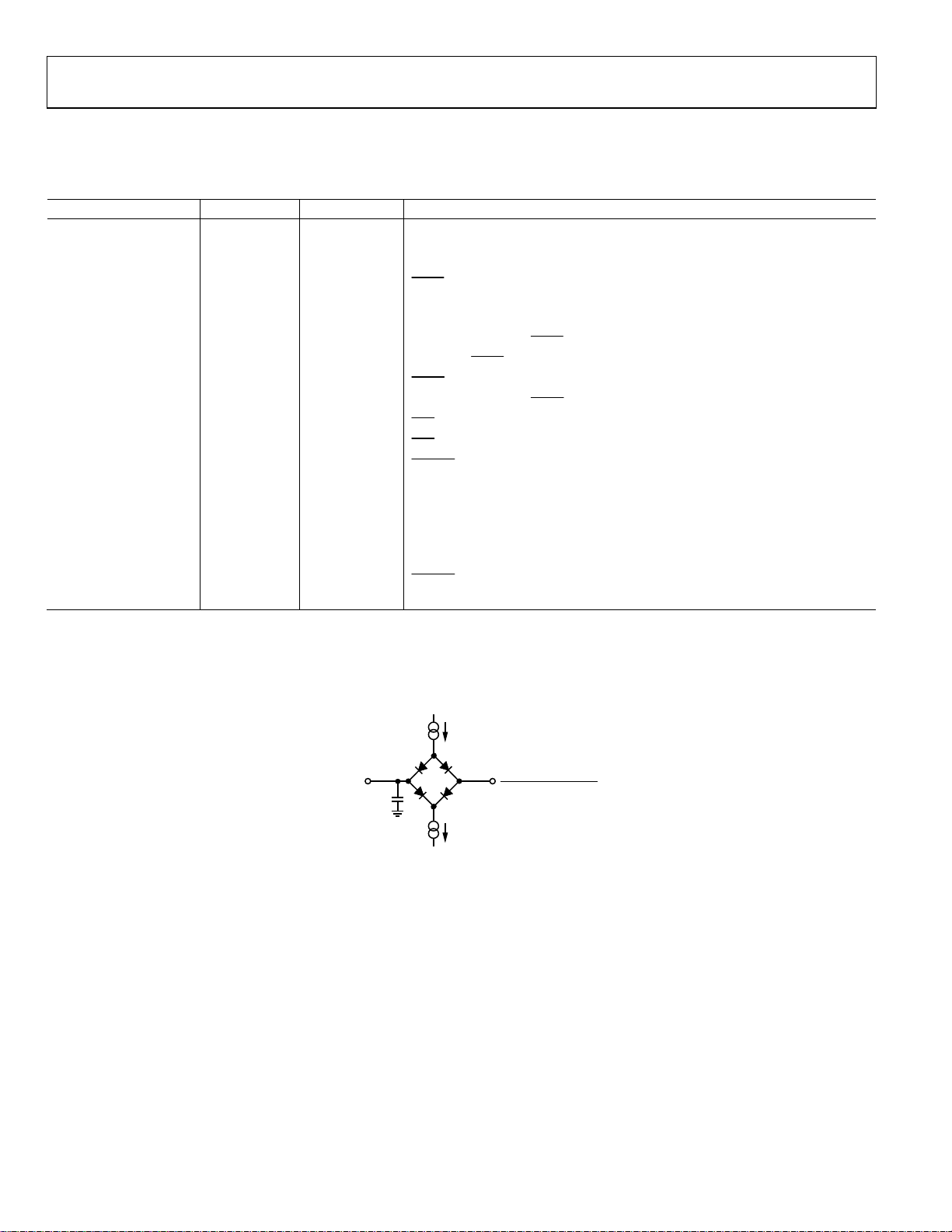
Under load conditions shown in Figure 2.
4
Time from when the VDD/V
5
Time required from execution of power-on software command to when the DAC outputs have settled to 1 V.
supplies are powered-up to when a digital interface command can be executed.
LOGIC
TO OUTPUT
PIN
50pF
C
200µA I
L
200µA I
OL
OH
Figure 2. Load Circuit for SDO Timing Diagram
Rev. A | Page 6 of 20
VOH (MIN) – VOL (MAX)
2
07994-002
 Loading...