Analog Devices AD5425 a Datasheet
8-Bit, High Bandwidth
FEATURES
2.5 V to 5.5 V supply operation
50 MHz serial interface
9.5 MSPS update rate
INL of ±0.25 LSB
10 MHz multiplying bandwidth
±10 V reference input
Low glitch energy: <2 nV-s
Extended temperature range: −40°C to +125°C
10-lead MSOP package
Guaranteed monotonic
4-quadrant multiplication
Power-on reset with brownout detection
function
LDAC
0.4 µA typical power consumption
APPLICATIONS
Portable battery-powered applications
Waveform generators
Analog processing
Instrumentation applications
Programmable amplifiers and attenuators
Digitally controlled calibration
Programmable filters and oscillators
Composite video
Ultrasound
Gain, offset, and voltage trimming
Multiplying DAC with Serial Interface
GENERAL DESCRIPTION
The AD54251 is a CMOS, 8-bit, current output digital-to-analog
converter that operates from a 2.5 V to 5.5 V power supply,
making it suitable for battery-powered applications and many
other applications.
This DAC utilizes a double buffered, 3-wire serial interface that
is compatible with SPI
interface standards. An
simultaneous updates in a multi-DAC configuration. On powerup, the internal shift register and latches are filled with 0s and
the DAC outputs are 0 V.
As a result of manufacturing on a CMOS submicron process,
this DAC offers excellent 4-quadrant multiplication characteristics with large signal multiplying bandwidths of 10 MHz.
The applied external reference input voltage (V
the full-scale output current. An integrated feedback resistor,
, provides temperature tracking and full-scale voltage output
R
FB
when combined with an external I-to-V precision amplifier.
The AD5425 is available in a small, 10-lead MSOP package.
1
U.S. Patent No. 5,969,657
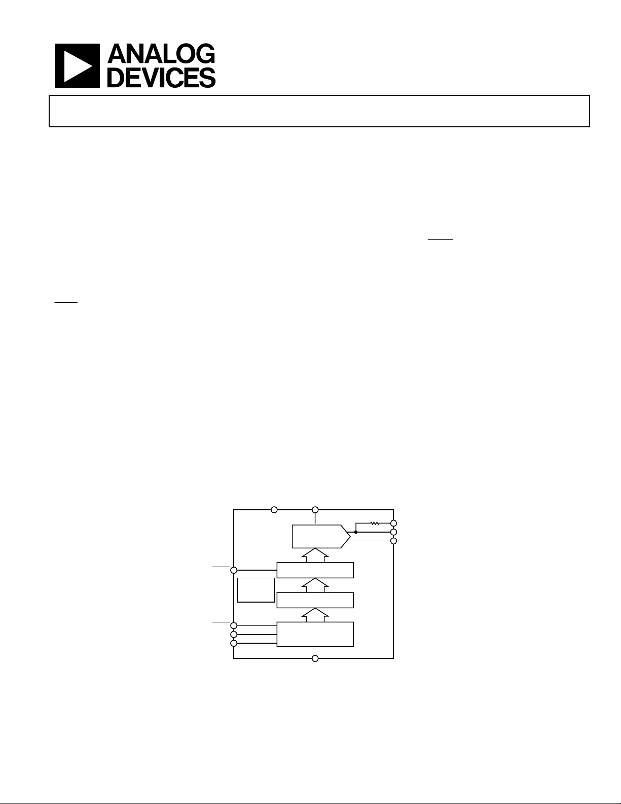
FUNCTIONAL BLOCK DIAGRAM
AD5425
V
DD
V
REF
8-BIT
R-2R DAC
R
AD5425
®, QSPI™, MICROWIRE™, and most DSP
pin is also provided, which allows
LDAC
REF
R
FB
I
1
OUT
I
2
OUT
) determines
LDAC
POWER-ON
RESET
SYNC
SCLK
SDIN
Rev. A
Information furnished by Analog Devices is believed to be accurate and reliable.
However, no responsibility is assumed by Analog Devices for its use, nor for any
infringements of patents or other rights of third parties that may result from its use.
Specifications subject to change without notice. No license is granted by implication
or otherwise under any patent or patent rights of Analog Devices. Trademarks and
registered trademarks are the property of their respective owners.
DAC REGISTER
INPUT LATCH
CONTROL LOGIC AND
INPUT SHIFT REGISTER
GND
Figure 1.
03161-001
One Technology Way, P.O. Box 9106, Norwood, MA 02062-9106, U.S.A.
Tel: 781.329.4700
Fax: 781.326.8703 © 2005 Analog Devices, Inc. All rights reserved.
www.analog.com

AD5425 Preliminary Technical Data
TABLE OF CONTENTS
Specifications..................................................................................... 3
Timing Characteristics..................................................................... 5
Absolute Maximum Ratings............................................................ 6
ESD Caution.................................................................................. 6
Pin Configuration and Function Descriptions............................. 7
Typical Performance Characteristics............................................. 8
Te r m in o l o g y .................................................................................... 13
Theory of Operation ...................................................................... 14
Circuit Operation ....................................................................... 14
Single-Supply Applications........................................................ 16
Positive Output Voltage ............................................................. 16
REVISION HISTORY
3/05—Rev. 0 to Rev. A
Updated Format................................................................ Universal
Changes to Specifications Section.................................................3
Added Figure 18, Figure 20, Figure 21........................................10
Change to Table 7 ..........................................................................18
Adding Gain................................................................................ 17
DACs Used as a Divider or Programmable Gain Element... 17
Reference Selection .................................................................... 17
Amplifier Selection .................................................................... 18
Serial Interface............................................................................ 19
Microprocessor Interfacing....................................................... 19
PCB Layout and Power Supply Decoupling................................ 22
Evaluation Board ........................................................................ 22
Operating the Evaluation Board .............................................. 22
Outline Dimensions....................................................................... 27
Ordering Guide .......................................................................... 27
2/04—Revision 0: Initial Version
Rev. A | Page 2 of 28

Preliminary Technical Data AD5425
SPECIFICATIONS
VDD = 2.5 V to 5.5 V, V
otherwise noted. DC performance measured with OP177, ac performance with AD8038, unless otherwise noted.
Table 1.
Parameter Min Typ Max Unit Conditions/Comments
STATIC PERFORMANCE
Resolution 8 Bits
Relative Accuracy ±0.25 LSB
Differential Nonlinearity ±0.5 LSB Guaranteed monotonic
Gain Error ±10 mV
Gain Error Temperature Coefficient ±5 ppm FSR/°C
Output Leakage Current ±10 nA Data = 0x0000, TA = 25°C, I
±20 nA Data = 0x0000, T = −40°C to +125°C, I
REFERENCE INPUT
Reference Input Range ±10 V
V
Input Resistance 8 10 12 kΩ Input resistance TC = −50 ppm/°C
REF
RFB Resistance 8 10 12 kΩ Input resistance TC = −50 ppm/°C
Input Capacitance
Code Zero Scale 3 6 pF
Code Full Scale 5 8 pF
DIGITAL INPUT/OUTPUT1
Input High Voltage, VIH 1.7 V
Input Low Voltage, VIL 0.6 V
Output High Voltage, VOH VDD − 1 V VDD = 4.5 V to 5 V, I
V
Output Low Voltage, VOL 0.4 V VDD = 4.5 V to 5 V, I
0.4 V VDD = 2.5 V to 3.6 V, I
Input Leakage Current, IIL 1 µA
Input Capacitance 4 10 pF
DYNAMIC PERFORMANCE1
Reference Multiplying Bandwidth 10 MHz V
Output Voltage Settling Time
Measured to ±1 mV 90 160 ns
Measured to ±4 mV 55 110 ns
Measured to ±16 mV 50 100 ns
Digital Delay 40 75 ns Interface delay time
10% to 90% Settling Time 15 30 ns Rise and fall time, V
Digital-to-Analog Glitch Impulse 2 nV-s 1 LSB change around major carry V
Multiplying Feedthrough Error DAC latch loaded with all 0s. V
70 dB 1 MHz
48 dB 10 MHz
Output Capacitance
I
1 12 17 pF All 0s loaded
OUT
25 30 pF All 1s loaded
I
2 22 25 pF All 0s loaded
OUT
10 12 pF All 1s loaded
Digital Feedthrough 0.1 nV-s
Analog THD 81 dB V
= 10 V, I
REF
1
2 = 0 V. Temperature range for Y version: −40°C to +125°C. All specifications T
OUT
− 0.5 V VDD = 2.5 V to 3.6 V, I
DD
= ±3.5 V, DAC loaded all 1s
REF
= ±3.5 V, R
V
REF
LOAD
MIN
= 200 µA
SOURCE
SOURCE
= 200 µA
SINK
= 200 µA
SINK
to T
OUT
= 200 µA
, unless
MAX
1
= 100 Ω, DAC latch
OUT
1
alternately loaded with 0s and 1s
= 10 V, R
REF
Feedthrough to DAC output with
= 100 Ω
LOAD
REF
= ±3.5 V
REF
SYNC high
= 0 V
and alternate loading of all 0s and all 1s
= 3.5 V p-p; all 1s loaded, f = 1 kHz
REF
Rev. A | Page 3 of 28

AD5425 Preliminary Technical Data
Parameter Min Typ Max Unit Conditions/Comments
Digital THD Clock = 1 MHz, V
50 kHz f
20 kHz f
Output Noise Spectral Density 25
70 dB
OUT
OUT
73 dB
Hz
nV√
@ 1 kHz
SFDR Performance (Wide Band) Clock = 2 MHz , V
50 kHz f
20 kHz f
67 dB
OUT
68 dB
OUT
SFDR Performance (Narrow Band) Clock = 2 MHz, V
50 kHz f
20 kHz f
Intermodulation Distortion 79 dB
73 dB
OUT
75 dB
OUT
= 20 kHz, f2 = 25 kHz, clock = 2 MHz,
f
1
V
= 3.5 V
REF
POWER REQUIREMENTS
Power Supply Range 2.5 5.5 V
IDD 0.6 µA TA = 25°C, logic inputs = 0 V or VDD
0.4 5 µA Logic inputs = 0 V or VDD, T = −40°C to +125°C
Power Supply Sensitivity 0.001 %/% ∆V
1
Guaranteed by design and characterization, not subject to production test.
= ±5%
DD
= 3.5 V, C
REF
= 3.5 V
REF
= 3.5 V
REF
COMP
= 1.8 pF
Rev. A | Page 4 of 28
Preliminary Technical Data AD5425
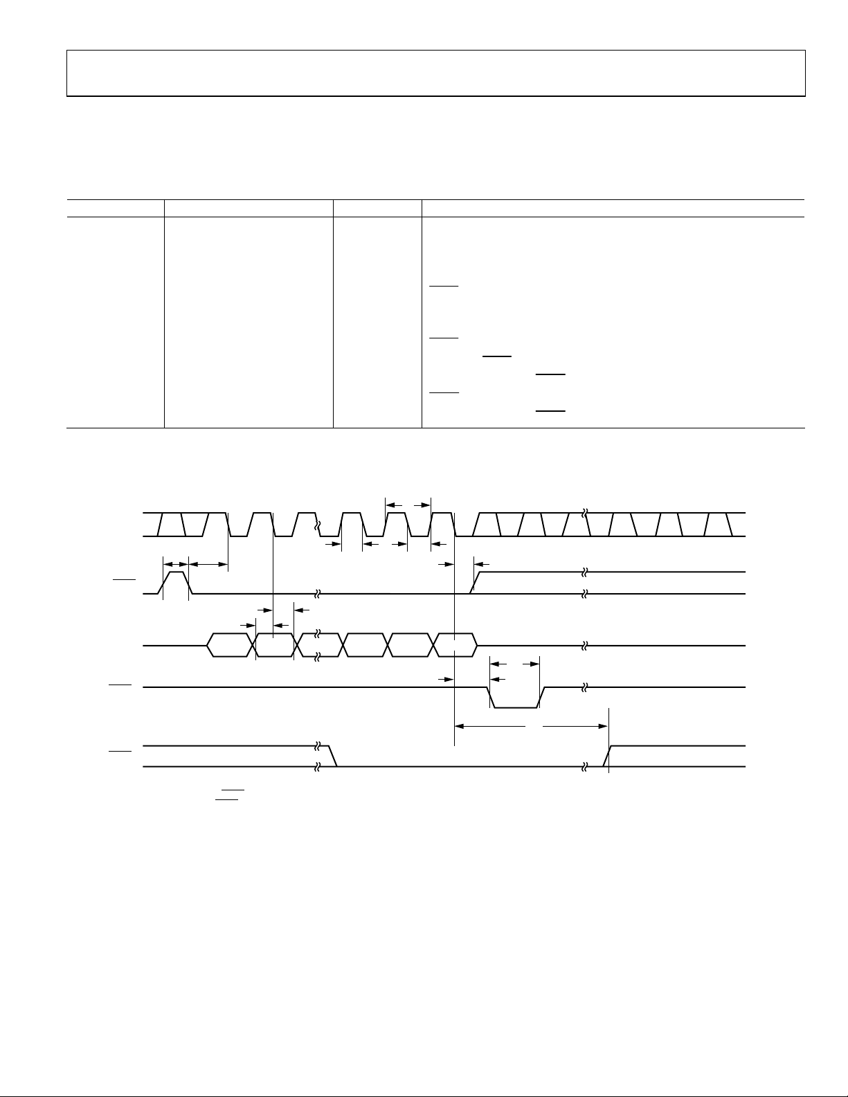
TIMING CHARACTERISTICS
All input signals are specified with tr = tf = 1 ns (10% to 90% of VDD) and timed from a voltage level of (VIL + VIH)/2. VDD =2.5 V to 5.5 V,
= 10 V, I
V
REF
Table 2. Timing Characteristics
Parameter
f
50 MHz max Maximum clock frequency
SCLK
t1 20 ns min SCLK cycle time
t2 8 ns min SCLK high time
t3 8 ns min SCLK low time
2
t
4
t5 5 ns min Data setup time
t6 3 ns min Data hold time
t7 5 ns min
t8 30 ns min
t9 0 ns min
t10 12 ns min
t11 10 ns min
1
Guaranteed by design and characterization, not subject to production test.
2
Falling or rising edge as determined by control bits of serial word.
2 = 0 V, temperature range for Y version: −40°C to +125°C ; all specifications T
OUT
1
VDD = 2.5 V to 5.5 V Unit Conditions/Comments
13 ns min
SYNC falling edge to SCLK falling edge setup time
SYNC rising edge to SCLK falling edge
Minimum
SYNC high time
SCLK falling edge to
LDAC pulse width
SCLK falling edge to
to T
MIN
MAX
LDAC falling edge
LDAC rising edge
, unless otherwise noted.
t
1
SCLK
t
t
8
4
SYNC
DIN
1
LDAC
2
LDAC
NOTES:
1
ASYNCHRONOUS LDAC UPDATE MODE.
2
SYNCHRONOUS LDAC UPDATE MODE.
DB7
t
2
t
6
t
5
t
3
t
7
DB0
t
t
10
9
t
11
03161-002
Figure 2. Timing Diagram
Rev. A | Page 5 of 28
AD5425 Preliminary Technical Data
ABSOLUTE MAXIMUM RATINGS
TA = 25°C, unless otherwise noted.
Table 3.
Parameter Rating
VDD to GND −0.3 V to +7 V
V
, RFB to GND −12 V to +12 V
REF
I
1, I
OUT
Logic Input and Output
2 to GND −0.3 V to VDD + 0.3 V
OUT
1
−0.3 V to VDD + 0.3 V
Operating Temperature Range
Extended Industrial (Y Version) −40°C to +125°C
Storage Temperature Range −65°C to +150°C
Junction Temperature 150°C
10-lead MSOP
θ
Thermal Impedance
JA
Lead Temperature, Soldering
206°C/W
300°C
(10 secs)
IR Reflow, Peak Temperature
235°C
(<20 secs)
Stresses above those listed under Absolute Maximum Ratings
may cause permanent damage to the device. This is a stress
rating only and functional operation of the device at these or
any other conditions above those listed in the operational
sections of this specification is not implied. Exposure to
absolute maximum rating conditions for extended periods may
affect device reliability. Only one absolute maximum rating may
be applied at any one time.
1
Overvoltages at SCLK,
Current should be limited to the maximum ratings given.
SYNC
, DIN, and
LDAC
are clamped by internal diodes.
ESD CAUTION
ESD (electrostatic discharge) sensitive device. Electrostatic charges as high as 4000 V readily accumulate on the
human body and test equipment and can discharge without detection. Although this product features
proprietary ESD protection circuitry, permanent damage may occur on devices subjected to high energy
electrostatic discharges. Therefore, proper ESD precautions are recommended to avoid performance
degradation or loss of functionality.
Rev. A | Page 6 of 28
Preliminary Technical Data AD5425
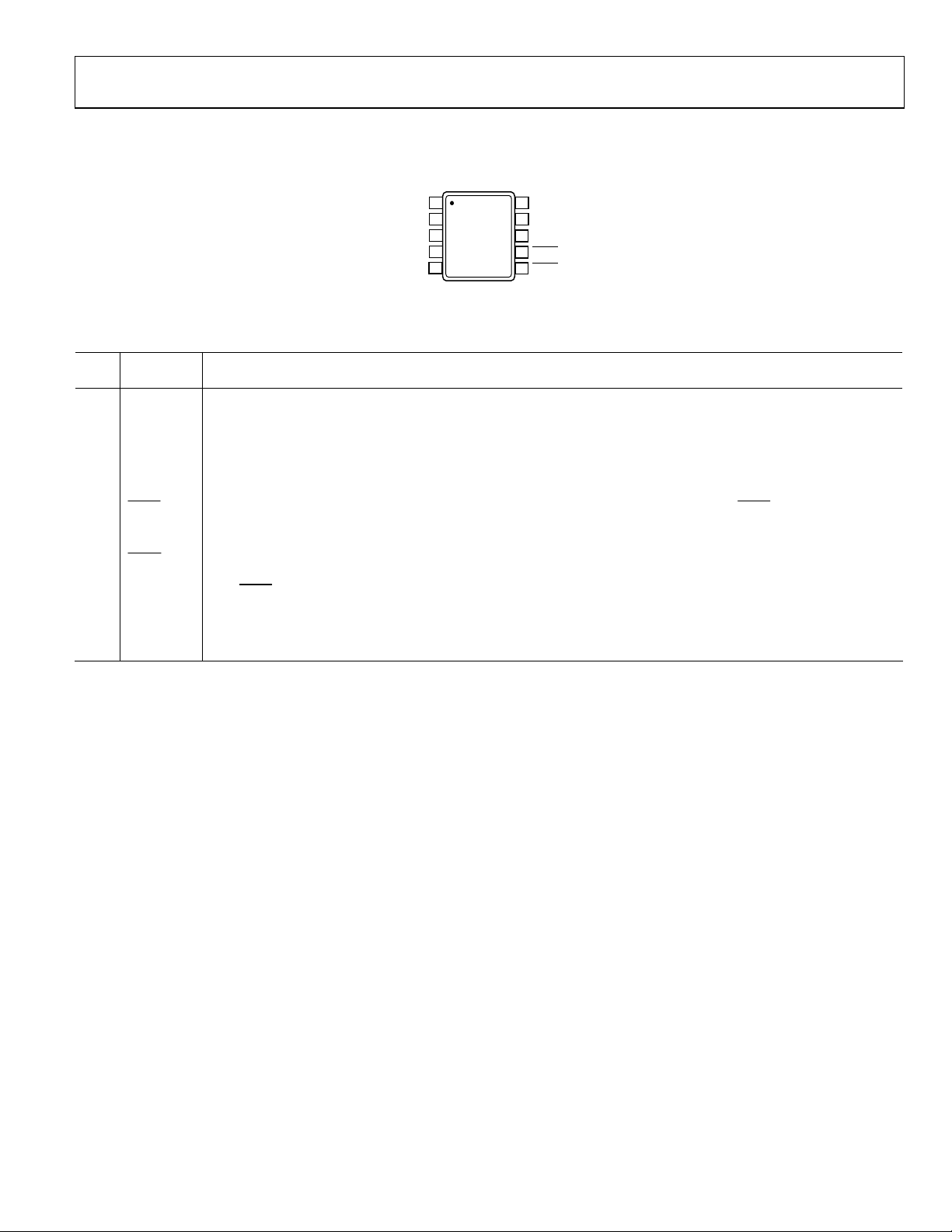
PIN CONFIGURATION AND FUNCTION DESCRIPTIONS
I
1
1
OUT
I
2
2
OUT
GND
SCLK
SDIN
AD5425
3
TOP VIEW
4
(Not to Scale)
5
Figure 3. Pin Configuration
Table 4. Pin Function Descriptions
Pin
No. Mnemonic Function
1 I
2 I
1 DAC Current Output.
OUT
2 DAC Analog Ground. This pin should normally be tied to the analog ground of the system.
OUT
3 GND Digital Ground Pin.
4 SCLK
Serial Clock Input. Data is clocked into the input shift register on each falling edge of the serial clock input.
This device can accommodate clock rates of up to 50 MHz.
5 SDIN Serial Data Input. Data is clocked into the 8-bit input register on each falling edge of the serial clock input.
6
SYNC
Active Low Control Input. This is the frame synchronization signal for the input data. When SYNC
on the SCLK and DIN buffers and the input shift register is enabled. Data is transferred on each falling edge of the
following 8 clocks.
7
LDAC
Load DAC Input. Updates the DAC output. The DAC is updated when this signal goes low or alternatively; if this line is
held permanently low, an automatic update mode is selected whereby the DAC is updated after 8 SCLK falling edges
SYNC
with
low.
8 VDD Positive Power Supply Input. This part can be operated from a supply of 2.5 V to 5.5 V.
9 V
DAC Reference Voltage Input Terminal.
REF
10 RFB DAC Feedback Resistor Pin. Establishes voltage output for the DAC by connecting to external amplifier output.
10
R
FB
9
V
REF
8
V
DD
LDAC
7
SYNC6
03161-003
goes low, it powers
Rev. A | Page 7 of 28
AD5425 Preliminary Technical Data
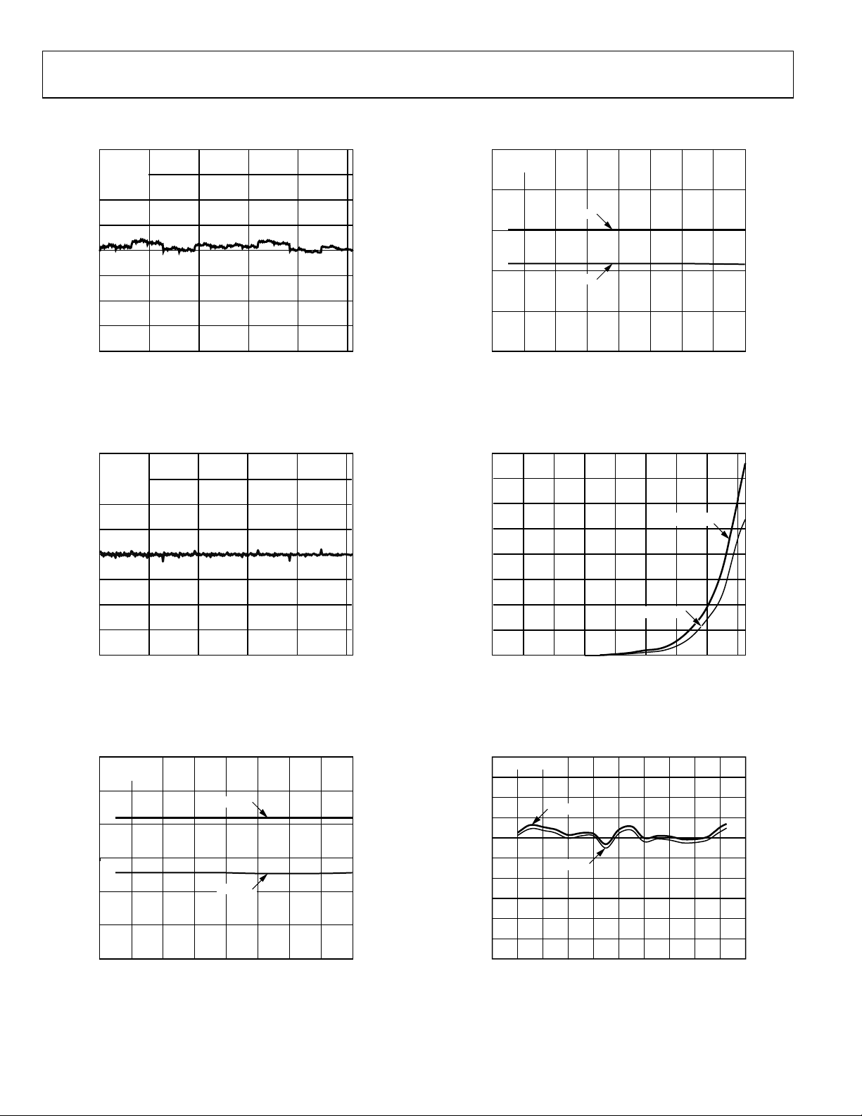
TYPICAL PERFORMANCE CHARACTERISTICS
INL (LSB)
0.20
0.15
0.10
0.05
–0.05
–0.10
–0.15
TA = 25°C
V
REF
VDD = 5V
0
= 10V
0.4
TA= 25°C
VDD= 5V
0.2
MIN DNL
0
–0.2
DNL (LSB)
–0.4
MAX DNL
INL (LSB)
INL (LSB)
–0.20
0.20
0.15
0.10
0.05
–0.05
–0.10
–0.15
–0.20
0.3
0.2
0.1
–0.1
–0.2
–0.3
TA = 25°C
V
V
0
TA= 25°C
V
0
Figure 4. INL vs. Code (8-Bit DAC)
= 10V
REF
= 5V
DD
Figure 5. DNL vs. Code (8-Bit DAC)
= 5V
DD
REFERENCE VOLTAGE
Figure 6. INL vs. Reference Voltage
CODE
CODE
MAX INL
MIN INL
2500 50 100 150 200
03161-004
–0.6
REFERENCE VOLTAGE
1023456789
xxxxx-xxx
Figure 7. DNL vs. Reference Voltage
1.6
1.4
1.2
I
1 VDD 5V
I
OUT
OUT
1 VDD 3V
120–40 –20 0 20 40 60 80 100
03161-008
140–60 –40 –20 0 20 40 60 80 100 120
03161-009
1.0
0.8
0.6
LEAKAGE (nA)
OUT
I
0.4
0.2
2500 50 100 150 200
03161-005
1023456789
xxxxx-xxx
0
TEMPERATURE (°C)
Figure 8. I
5
V
= 10V
REF
4
3
2
1
0
–1
ERROR (mV)
–2
–3
–4
–5
1 Leakage Current vs. Temperature
OUT
VDD = 5V
VDD = 2.5V
TEMPERATURE (°C)
Figure 9. Gain Error vs. Temperature
Rev. A | Page 8 of 28
Preliminary Technical Data AD5425
LSBs
–0.1
–0.3
0.5
0.3
0.1
TA = 25°C
VDD = 3V
V
= 0V
REF
MAX INL
MIN INL
MAX DNL
MIN DNL
2.5
VDD = 5V
V
= 0V
REF
2.0
1.5
1.0
VOLTAGE (mV)
0.5
0
GAIN ERROR
OFFSET ERROR
–0.5
V
BIAS
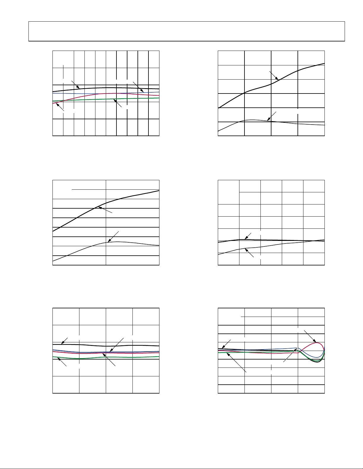
Figure 10. Linearity vs. V
1.4
TA = 25°C
= 3V
V
DD
1.2
V
= 0V
REF
1.0
0.8
0.6
0.4
VOLTAGE(mV)
0.2
0
–0.2
–0.4
BIAS
V
BIAS
Figure 11. Gain and Offset Errors vs. V
(V)
Voltage Applied to I
GAIN ERROR
OFFSET ERROR
(V)
Voltage Applied to I
BIAS
OUT
1.50.5 0.6 0.7 0.8 0.9 1.0 1.1 1.2 1.3 1.4
03161-010
2
1.50.5 1.0
03161-011
2
OUT
–0.5
V
(V)
BIAS
Figure 13. Gain and Offset Errors vs. Voltage Applied to I
10.0
TA = 25°C
= 5V
V
DD
V
= 2.5V
8.0
REF
6.0
4.0
2.0
VOLTAGE (mV)
0
–2.0
–4.0
Figure 14. Gain and Offset Errors vs. V
OFFSET ERROR
GAIN ERROR
V
(V)
BIAS
Voltage Applied to I
BIAS
OUT
2.50.5 1.0 1.5 2.0
2.50 0.5 1.0 1.5 2.0
OUT
03161-013
2
03161-014
2
0.5
VDD = 5V
V
= 0V
REF
0.3
0.1
LSBs
–0.1
–0.3
–0.5
Figure 12. Linearity vs. V
MAX INL
MIN DNL
MIN INL
V
(V)
BIAS
Voltage Applied to I
BIAS
MAX DNL
OUT
1.0
TA = 25°C
= 5V
V
DD
0.8
= 2.5V
V
REF
0.6
0.4
0.2
LSBs
–0.2
–0.4
–0.6
–0.8
2.50.5 1.0 1.5 2.0
03161-012
–1.0
2
MAX INL BIAS
0
MAX DNL BIAS
MIN DNL BIAS
Figure 15. Linearity vs. V
MIN INL BIAS
V
(V)
BIAS
Voltage Applied to I
BIAS
OUT
2.00 0.5 1.0 1.5
03161-015
2
Rev. A | Page 9 of 28
 Loading...