Analog Devices AD5405 Datasheet
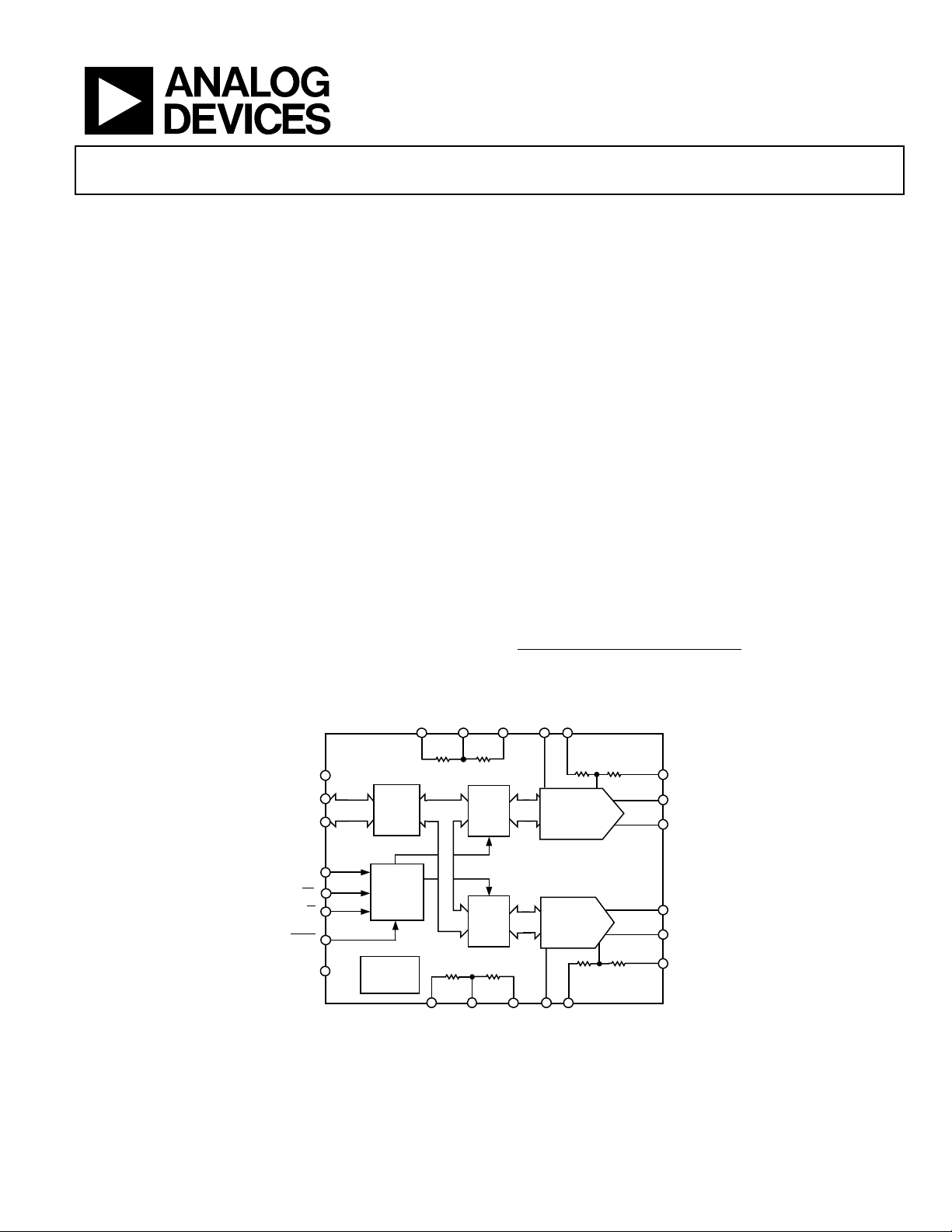
Dual 12-Bit, High Bandwidth, Multiplying DAC with
4-Quadrant Resistors and Parallel Interface
FEATURES
On chip 4-quadrant resistors allow flexible output ranges
10 MHz multiplying bandwidth
Fast parallel interface write cycle: 58 MSPS
2.5 V to 5.5 V supply operation
±10 V reference input
Extended temperature range: −40°C to 125°C
40-lead LFCSP package
Guaranteed monotonic
4-quadrant multiplication
Power-on reset
Readback function
.5 µA typical current consumption
APPLICATIONS
Portable battery-powered applications
Waveform generators
Analog processing
Instrumentation applications
Programmable amplifiers and attenuators
Digitally-controlled calibration
Programmable filters and oscillators
Composite video
Ultrasound
Gain, offset, and voltage trimming
R3A R2AR2_3A
AD5405
V
DD
DATA
DB0
INPUTS
DB11
INPUT
BUFFER
AD5405
GENERAL DESCRIPTION
The AD54051 is a dual CMOS, 12-bit, cur rent output dig italto-analog converter (DAC).This device operates from a 2.5 V to
5.5 V power supply, making it suited to battery-powered and
other applications.
The applied external reference input voltage (V
the full-scale output current. An integrated feedback resistor
) provides temperature tracking and full-scale voltage
(R
FB
output when combined with an external I-to-V precision
amplifier. This device also contains all the 4-quadrant resistors
necessary for bipolar operation and other configuration modes.
This DAC utilizes data readback, allowing the user to read the
contents of the DAC register via the DB pins. On power-up, the
internal register and latches are filled with zeros and the DAC
outputs are at zero scale.
As a result of manufacture with a CMOS submicron process, the
device offers excellent 4-quadrant multiplication characteristics,
with large signal multiplying bandwidths of up to 10 MHz.
The AD5405 has a 6 mm × 6 mm, 40-lead LFCSP package.
1
US Patent Number 5,689,257.
V
A
REF
R1A
R2
R3
2R
2R
LATCH
R1
2R
12-BIT
R-2R DAC A
RFB
2R
R
I
I
OUT
OUT
A
FB
1A
2A
) determines
REF
DAC A/B
CS
R/W
LDAC
GND
CONTROL
LOGIC
POWER-ON
RESET
R3
2R
R3B R2BR2_3B
Figure 1. AD5405 Functional Block Diagram
Rev. 0
Information furnished by Analog Devices is believed to be accurate and reliable.
However, no responsibility is assumed by Analog Devices for its use, nor for any
infringements of patents or other rights of third parties that may result from its use.
Specifications subject to change without notice. No license is granted by implication
or otherwise under any patent or patent rights of Anal og Devices. Trademarks and
registered trademarks are the property of their respective owners.
I
1B
LATCH
R2
2R
12-BIT
R-2R DAC B
R1
RFB
2R
2R
V
B
R1B
REF
One Technology Way, P.O. Box 9106, Norwood, MA 02062-9106, U.S.A.
Tel: 781.329.4700
Fax: 781.326.8703 © 2004 Analog Devices, Inc. All rights reserved.
www.analog.com
OUT
I
OUT
RFB B
2B
04463-0-001

AD5405
TABLE OF CONTENTS
Specifications..................................................................................... 3
Timing Characteristics..................................................................... 5
Absolute Maximum Ratings............................................................ 6
ESD Caution.................................................................................. 6
Pin Configuration and Function Descriptions............................. 7
Typical Performance Characteristics ............................................. 8
Te r m in o l o g y .................................................................................... 13
General Description....................................................................... 14
DAC Section................................................................................ 14
Circuit Operation ....................................................................... 14
Single-Supply Applications........................................................ 15
Positive Output Voltage ............................................................. 15
REVISION HISTORY
7/04—Revision 0: Initial Version
Adding Gain................................................................................ 15
Used as a Divider or Programmable Gain Element............... 16
Reference Selection .................................................................... 16
Amplifier Selection .................................................................... 16
Parallel Interface ......................................................................... 17
Microprocessor Interfacing....................................................... 17
PCB Layout and Power Supply Decoupling ........................... 17
Evaluation Board for the DACs................................................ 18
Overview of AD54xx Devices....................................................... 22
Outline Dimensions....................................................................... 23
Ordering Guide .......................................................................... 23
Rev. 0 | Page 2 of 24

AD5405
REF
IH
IL
1
A = V
IL
OL
OH
OL
OH
B = 10 V, I
REF
2
2 = 0 V. All specifications T
OUT
MIN
to T
unless otherwise noted. DC performance measured
MAX,
±5 ppm FSR/°C
1
OUT
Typical resistor TC = −50 ppm/°C
1.6 2.5 % Typ = 25°C, Max = 125°C
1.7 V VDD = 2.5 V to 5.5 V
0.8 V VDD = 2.7 V to 5.5 V
1 µA
0.4 V I
VDD − 1 V I
0.4 V I
VDD −0.5 V I
= 200 µA
SINK
= 200 µA
SOURCE
= 200 µA
SINK
= 200 µA
SOURCE
= 5 V pk-pk, DAC loaded all 1s
REF
DAC latch alternately loaded with 0s and 1s.
Feedthrough to DAC output with
alternate loading of all 0s and all 1s
= 5 V p-p, all 1s loaded, f = 1 kHz
REF
= 5 V, sine wave generated from digital code
REF
OUT
1
LOAD
= 100 Ω, C
= 0 V
REF
CS high and
LOAD
=15 pF.
SPECIFICATIONS
VDD = 2.5 V to 5.5 V, V
with OP1177, AC performance with AD9631, unless otherwise noted.
Table 1.
Parameter Min Typ Max Unit Conditions
STATIC PERFORMANCE
Resolution 12 Bits
Relative Accuracy ±1 LSB
Differential Nonlinearity −1/+2 LSB Guaranteed monotonic
Gain Error ±25 mV
Gain Error Temp Coefficient
Bipolar Zero-Code Error ±25 mV
Output Leakage Current ±1 nA Data = 0x0000, TA = 25°C, I
±10 nA Data = 0x0000H, I
REFERENCE INPUT2
Reference Input Range ±10 V
V
A, V
REF
V
REF
Mismatch
R1, RFB Resistance 16 20 24 kΩ
R2, R3 Resistance 16 20 24 kΩ
R2 to R3 Resistance Mismatch .06 .18 % Typ = 25°C, Max = 125°C
DIGITAL INPUTS/OUTPUT2
Input High Voltage, V
Input Low Voltage, V
0.7 V VDD = 2.5 V to 2.7 V
Input Leakage Current, I
Input Capacitance 10 pF
VDD = 4.5 V to 5.5 V
VDD = 2.5 V to 3.6 V
DYNAMIC PERFORMANCE2
Reference Multiplying BW 10 MHz V
Output Voltage Settling Time 80 120 ns Measured to ±1 mV of FS. R
Digital Delay 20 40 ns
Digital-to-Analog Glitch Impulse 3 nV-s 1 LSB change around major carry, V
Multiplying Feedthrough Error −75 dB DAC latch loaded with all 0s. Reference = 10 kHz
Output Capacitance 2 pF DAC latches loaded with all 0s
4 pF DAC latches loaded with all 1s
Digital Feedthrough 5 nV-s
Total Harmonic Distortion −75 dB V
−75 dB V
Output Noise Spectral Density 25 nV/√Hz @ 1 kHz
B Input Resistance 8 10 12 kΩ DAC input resistance
REF
A to V
B Input Resistance
REF
Output Low Voltage, V
Output High Voltage, V
Output Low Voltage, V
Output High Voltage, V
Rev. 0 | Page 3 of 24

AD5405
Parameter Min Typ Max Unit Conditions
SFDR Performance (Wideband)
Clock = 10 MHz
500 kHz f
100 kHz f
50 kHz f
OUT
OUT
OUT
Clock = 25 MHz
500 kHz f
100 kHz f
50 kHz f
OUT
OUT
OUT
SFDR Performance (Narrow Band)
Clock = 10 MHz
500 kHz f
100 kHz f
50k Hz f
OUT
OUT
OUT
Clock = 25 MHz
500 kHz f
100 kHz f
50k Hz f
OUT
OUT
OUT
Intermodulation Distortion
Clock = 10 MHz
f1 = 400 kHz, f2 = 500 kHz 65 dB
f1 = 40 kHz, f2 = 50 kHz 72 dB
Clock = 25 MHz
f1 = 400 kHz, f2 = 500 kHz 51 dB
f1 = 40 kHz, f2 = 50 kHz 65 dB
POWER REQUIREMENTS
Power Supply Range 2.5 5.5 V
I
DD
Power Supply Sensitivity2 0.001 %/% ∆VDD = ±5%
1
Temperature range for Y version is −40°C to +125°C.
2
Guaranteed by design, not subject to production test.
55 dB
63 dB
65 dB
50 dB
60 dB
62 dB
73 dB
80 dB
87 dB
70 dB
75 dB
80 dB
10 µA Logic inputs = 0 V or V
DD
Rev. 0 | Page 4 of 24
AD5405
TIMING CHARACTERISTICS
VDD = 2.5 V to 5.5 V, V
Table 2.
Parameter
1, 2
Write Mode
t
1
t
2
t
3
t
4
t
5
t
6
t
7
t
8
t
9
Data Readback Mode
t
10
t
11
t
12
35 ns max
t
13
10 ns max
1
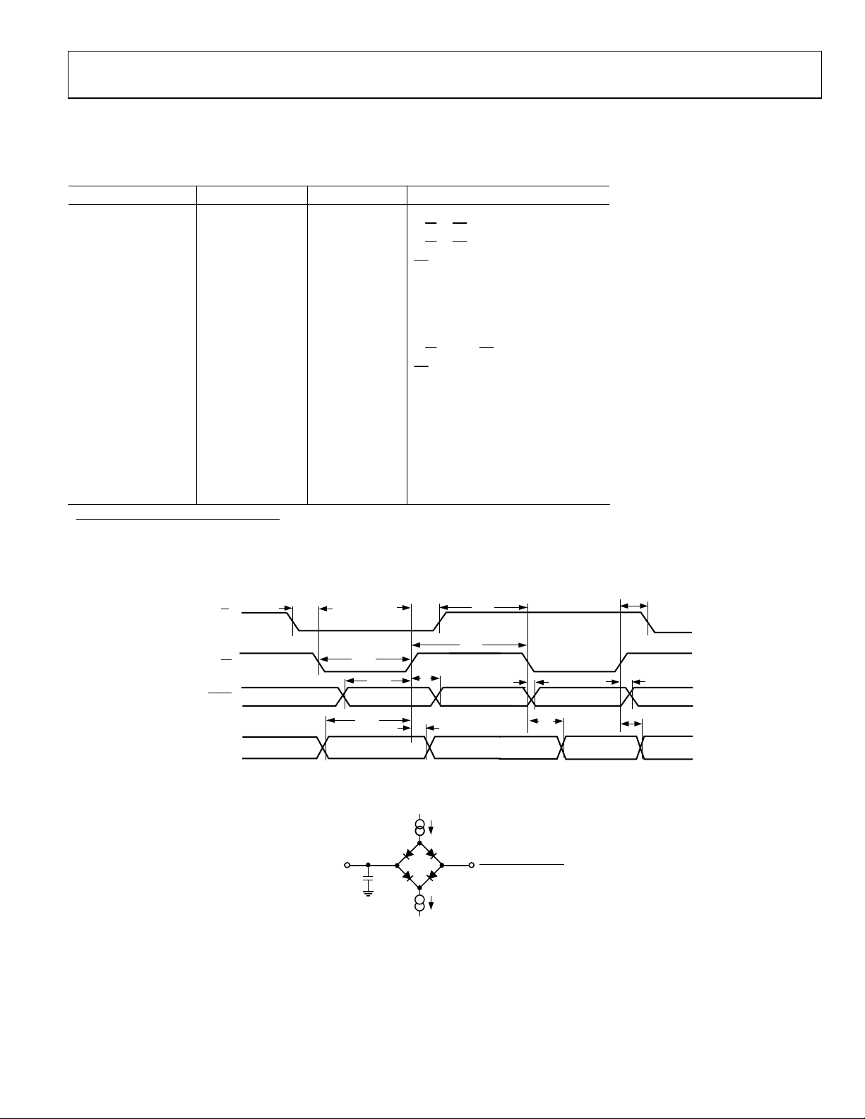
See Temperature range for Y version is −40°C to +125°C. Guaranteed by design and characterization, not subject to production test. Figure 2.
2
All input signals are specified with tr = tf = 5ns (10% to 90% of VDD) and timed from a voltage level of (VIL + VIH)/2. Digital output timing measured
with load circuit in . Figure 3
= 5 V, I
REF
Limit at T
0 ns min
0 ns min
10 ns min
2 = 0 V. All specifications T
OUT
MIN
, T
Unit Conditions/Comments
MAX
to T
MIN
W to CS setup time
R/
W to CS hold time
R/
unless otherwise noted.
MAX,
CS low time
10 ns min Address setup time
0 ns min Address hold time
6 ns min Data setup time
0 ns min Data hold time
5 ns min
7 ns min
W high to CS low
R/
CS min high time
0 ns typ Address setup time
0 ns typ Address hold time
5 ns typ Data access time
5 ns typ Bus relinquish time
t
R/W
t
1
t
2
8
t
2
t
9
t
10
t
t
7
12
t
11
DATA VALID
t
13
04463-0-002
DACA/DACB
DATA
CS
t
3
t
4
t
6
DATA VALID
t
5
Figure 2. Timing Diagram
I
OL
V
+ V
OH (MIN)
I
OH
OL (MAX)
2
04463-0-003
TO
OUTPUT
PIN
C
L
50pF
200µA
200µA
Figure 3. Load Circuit for Data Timing Specifications
Rev. 0 | Page 5 of 24
AD5405
ABSOLUTE MAXIMUM RATINGS
TA = 25°C, unless otherwise noted.
Table 3.
Parameter Rating
VDD to GND
V
A, V
REF
I
OUT
B, RFBA, RFBB to GND
REF
1, I
2 to GND
OUT
Logic Inputs and Output
1
−0.3 V to +7 V
−12 V to +12 V
−0.3 V to +7 V
−0.3V to VDD + 0.3 V
Operating Temperature Range
Automotive (Y Version)
Storage Temperature Range
−40°C to +125°C
−65°C to +150°C
Junction Temperature 150°C
40-lead LFCSP, θJA Thermal Impedance 30°C/W
Lead Temperature, Soldering (10 sec.) 300°C
IR Reflow, Peak Temperature (< 20 sec.) 235°C
1
Over voltages at DBx,
Current should be limited to the maximum ratings given.
LDAC, CS
, and W/R are clamped by internal diodes.
ESD CAUTION
ESD (electrostatic discharge) sensitive device. Electrostatic charges as high as 4000 V readily accumulate on
the human body and test equipment and can discharge without detection. Although this product features
proprietary ESD protection circuitry, permanent damage may occur on devices subjected to high energy
electrostatic discharges. Therefore, proper ESD precautions are recommended to avoid performance
degradation or loss of functionality.
Stresses above those listed under Absolute Maximum Ratings
may cause permanent damage to the device. This is a stress
rating only; functional operation of the device at these or any
other conditions above those indicated in the operational
sections of this specification is not implied. Exposure to
absolute maximum rating conditions for extended periods may
affect device reliability.
Rev. 0 | Page 6 of 24
AD5405
PIN CONFIGURATION AND FUNCTION DESCRIPTIONS
R1A
R2A
R2_3A
R3A
V
REF
DGND
LDAC
DAC A/B
NC
DB11
A
2
1A
A
FB
OUT
OUT
40 R
39 I
38 I
1
2
3
4
A
5
6
7
8
9
10
PIN 1
INDICATOR
AD5405
TOP VIEW
B
B
1
2
B
FB
OUT
37 NC
36 NC
OUT
35 NC
34 NC
33 I
32 I
31 R
30 R1B
29 R2B
28 R2_3B
27 R3B
B
26 V
REF
25 V
DD
24 CLR
23 R/W
22 CS
21 DB0
NC = NO CONNECT
DB10 11
DB5 16
DB9 12
DB8 13
DB7 14
DB6 15
DB4 17
DB2 19
DB1 20
DB3 18
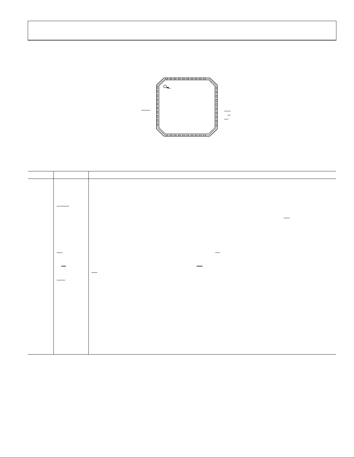
Figure 4. Pin Configuration
Table 4. Pin Function Descriptions
Pin No. Mnemonic Function
1 to 4 R1A to R3A
DAC A 4-Quadrant Resistors. Allow a number of configuration modes, including bipolar operation with
minimum of external components.
5, 26 V
REF
A, V
B DAC Reference Voltage Input Terminals.
REF
6 DGND Digital Ground Pin.
7
LDAC Load DAC Input. Allows asynchronous or synchronous updates to the DAC output. The DAC is asynchronously
updated when this signal goes low. Alternatively, if this line is held permanently low, an automatic or
synchronous update mode is selected whereby the DAC is updated on the rising edge of
8 DAC A/B Selects DAC A or B. Low selects DAC A, while high selects DAC B.
9, 34, 35,
NC Not internally connected.
36, 37
10 to 21 DB11 to DB0 Parallel Data Bits 11 through 0.
22
CS Chip Select Input. Active low. Used in conjunction with R/W to load parallel data to the input latch or to read
data from the DAC register. Edge sensitive; when pulled high, the DAC data is latched.
23
W Read/Write. When low, used in conjunction with CS to load parallel data. When high, used in conjunction with
R/
CS to read back contents of DAC register.
24
25 V
CLR
DD
26 to 30 R3B to R1B
Active Low Control Input. Clears DAC output and input and DAC registers.
Positive Power Supply Input. These parts can be operated from a supply of 2.5 V to 5.5 V.
DAC B 4-Quadrant Resistors. Allow a number of configuration modes, including bipolar operation with a
minimum of external components.
32 I
OUT
2B
DAC A Analog Ground. This pin typically should be tied to the analog ground of the system, but may be biased
to achieve single-supply operation.
33 I
38 I
39 I
1B DAC B Current Outputs.
OUT
1A DAC A Current Outputs.
OUT
OUT
2A
DAC A Analog Ground. This pin typically should be tied to the analog ground of the system, but may be biased
to achieve single-supply operation.
31, 40 RFBB, RFBA External Amplifier Output.
04463-0-004
CS.
Rev. 0 | Page 7 of 24
AD5405
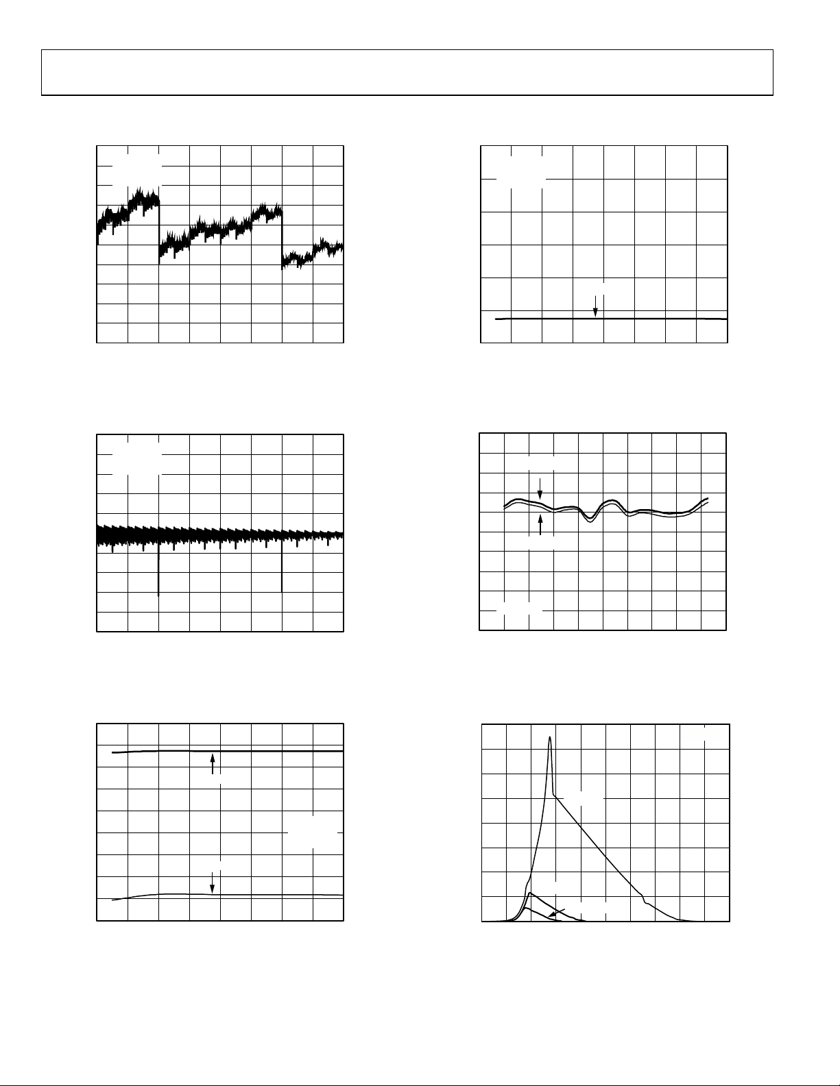
TYPICAL PERFORMANCE CHARACTERISTICS
1.0
TA = 25°C
INL (LSB)
DNL (LSB)
INL (LSB)
0.8
0.6
0.4
0.2
0
–0.2
–0.4
–0.6
–0.8
–1.0
1.0
0.8
0.6
0.4
0.2
0
–0.2
–0.4
–0.6
–0.8
–1.0
0.6
0.5
0.4
0.3
0.2
0.1
0
–0.1
–0.2
–0.3
= 10V
V
REF
= 5V
V
DD
20001500500 10000 2500 3000 3500 4000
CODE
Figure 5. INL vs. Code (12-Bit DAC)
TA = 25°C
= 10V
V
REF
= 5V
V
DD
20001500500 10000 2500 3000 3500 4000
CODE
Figure 6. DNL vs. Code (12-Bit DAC)
MAX INL
MIN INL
65342 78910
REFERENCE VOLTAGE
Figure 7. INL vs. Reference Voltage
TA = 25°C
V
= 10V
REF
= 5V
V
DD
04463-0-030
04463-0-031
04463-0-032
–0.40
TA = 25°C
V
= 10V
–0.45
–0.50
–0.55
DNL (LSB)
–0.60
–0.65
–0.70
REF
V
= 5V
DD
MIN DNL
65342789
REFERENCE VOLTAGE
Figure 8. DNL vs. Reference Voltage
5
4
3
2
1
0
–1
ERROR (mV)
–2
–3
–4
–5
–60 –40 –20 0 20 40 60 80 100 120 140
VDD = 5V
= 2.5V
V
DD
V
= 10V
REF
TEMPERATURE (°C)
Figure 9. Gain Error vs. Temperature
8
7
6
5
4
3
CURRENT (mA)
2
1
0
1.00.50
VDD = 5V
VDD = 3V
VDD = 2.5V
INPUT VOLTAGE (V)
Figure 10. Supply Current vs. Logic Input Voltage
10
04463-0-034
04463-0-034
TA = 25°C
4.54.03.53.02.52.01.5
5.0
04463-0-013
Rev. 0 | Page 8 of 24
 Loading...