

Full Accurate 16 Bit Vout nanoDac
2.7V- 5.5V, in a Sot 23
TM
,
Preliminary Technical Data
FEATURES
Single 16-Bit DAC, 1Lsb inl.
1.8 Volt Digital Interface Capability
Power-On-Reset to Zero Volts/Mid Scale
Three Power-Down Functions
Low Power Serial Interface with SchmittTriggered Inputs
8-Lead Sot23, 10-Lead MSOP Package
Low Power
Fast Settling 3us.
2.7-5.5 V Power Supply
Low Glitch on Powerup.
Unbuffered Voltage Capable of driving
60k Ohm load.
APPLICATIONS
Process Control
Data Acquisition Systems
Portable Battery Powered Instruments
Digital Gain and Offset Adjustment
Programmable Voltage and Current Sources
Programmable Attenuators
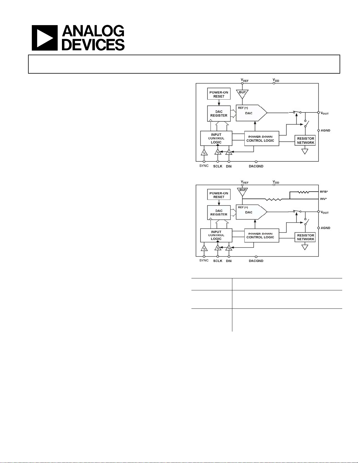
GENERAL DESCRIPTION
The AD5062/AD5063, a member of the nanoDAC
are single 16-bit unbuffered voltage out DACs that operate
from a single 2.7-5V supply. The AD5062 version is available
in a 8 ld Sot23. The AD5063 version is available with on board
resistors in a 10 ld uSOIC, making it easy to generate bipolar
signals on the output.
The parts utilize a versatile three-wire serial interface that
operates at clock rates up to 30 MHz and is compatible with
standard SPI™, QSPI™, MICROWIRE™ and DSP interface
standards.
The reference for AD5062/AD5063 is supplied from an
external REF pin. A reference buffer is also provided on chip.
The part incorporates a power-on-reset circuit that ensures that
the DAC output powers up to zero volts/ mid scale and remains
there until a valid write takes place to the device. The part
contains a power-down feature that reduces the current
consumption of the device to 50nA at 5 V and provides
software selectable output loads while in power-down mode.
The part is put into power-down mode over the serial interface.
Total unadjusted error for the part is <1mV.
These parts also provide a very low glitch on power-up.
Rev. PrC
Information furnished by Analog Devices is believed to be accurate and reliable.
However, no responsibility is assumed by Analog Devices for its use, nor for any
infringements of patents or other rights of third parties that may result from its use.
Specifications subject to change without notice. No license is granted by implication
or otherwise under any patent or patent rights of Analog Devices. Trademarks and
registered trademarks are the property of their respective owners.
TM
family,
AD5062/AD5063
AD5062 8 Ld Sot23.
AD5063. 10 Ld MSOP.
Part Number Description
AD5061
AD5040/60
2.7 V to 5.5 V, 16 Bit
Sot 23
2.7 V to 5.5 V, 14/16 Bit
INL, Sot23.
nano
nano
PRODUCT HIGHLIGHTS
1. Available in 8-lead SOT23, 10-lead MSOP.
2. 16 Bit Accurate, 1 LSB INL.
3. Low Glitch on Power-up.
4. High speed serial interface with clock speeds up to 30 MHz.
5. Three power down modes available to the user.
One Technology Way, P.O. Box 9106, Norwood, MA 02062-9106, U.S.A.
Tel: 781.329.4700 www.analog.com
Fax: 781.326.8703 © 2005 Analog Devices, Inc. All rights reserved.
DAC
DAC
TM
D/A, 4 LSBs INL,
TM
D/A, 1 LSBs

AD5062/AD5063 Preliminary Technical Data
AD5062/AD5063—SPECIFICATIONS1
(VDD = 2.7-5.5 V, Vref =4.096V @ VDD = 5.0V . T
Parameter B Version1
STATIC PERFORMANCE
AD5062/AD5063
Resolution 16 Bits
Relative Accuracy ±1 LSB
TUE 0.5 mV
Differential Nonlinearity ±1 LSB Guaranteed Monotonic by Design.
Offset Error 0.65 % of FSR
Zero Code Error 100 mv All 0’s loaded to dac reg
Full scale Error +/-0.01 mv All 1’s loaded to dac reg
Gain Error +/- 0.04 % of FSR
Zero code Error Drift 6 µV/°C
Gain Temperature Coefficient 2.5 ppm of FSR
AD5063
Bipolar Resistor Matching +/-0.025 % Ratio Error
Bipolar Zero Offset Error 1 mV
Bipolar Zero Temperature Co-ef. 2 uV/oC
OUTPUT CHARACTERISTICS
Output Voltage Range
Output Voltage Settling Time 3 µs CODE TBD
Slew Rate 1 V/µs
Output Noise Spectral Density
50
Digital-to-Analog Glitch
Impulse
Digital Feedthrough 0.5 nV-s
DC Output Impedance 12
REFERENCE INPUT/OUPUT
Vref Input Range
Input Current 1
DC Input Impedance 1
LOGIC INPUTS
Input Current ±1 µA
V
, Input Low Voltage
INL
V
, Input High Voltage
INH
Pin Capacitance 3 pF
POWER REQUIREMENTS
VDD
I
(Normal Mode)
DD
VDD = +2.7 V to +5.5 V
IDD (All Power-Down Modes)
VDD = +2.7 V to +5.5 V
POWER EFFICIENCY
to T
MIN
unless otherwise noted)
MAX
Unit Test Conditions/Comments
Min Typ Max
0 V
50
ref
-100mv
V
nV/√Hz
nV/√Hz
DAC code=TBD , 1kHz
DAC code=TBD , 10kHz
5 nV-s 1 LSB Change Around Major Carry.
ΚΩ
2 V
DD-100mV
uA
MΩ
0.8 V
2. 0 V
2.7 5.5 V
VDD = +2.7 to +5.5 V
VDD = +2.7 to +5.5 V
All Digital Inputs at Zero or VDD
DAC Active and Excluding Load Current
600 µA
VIH = VDD and VIL = GND
50 nA
VIH = VDD and VIL = GND
Rev. Pr C | Page 2 of 19

Preliminary Technical Data AD5062/AD5603
Parameter B Version1
Min Typ Max
I
OUT/IDD
TBD %
PSSR 0.5 LSB VDD +/- 10%
NOTES
1
Temperature ranges are as follows: B Version: –40°C to +125°C, typical at 25°C.
2
Guaranteed by design and characterization, not production tested.
Specifications subject to change without notice.
Unit Test Conditions/Comments
I
= 2 mA. VDD = +5 V
LOAD
Rev. Pr C | Page 3 of 19
AD5062/AD5063 Preliminary Technical Data
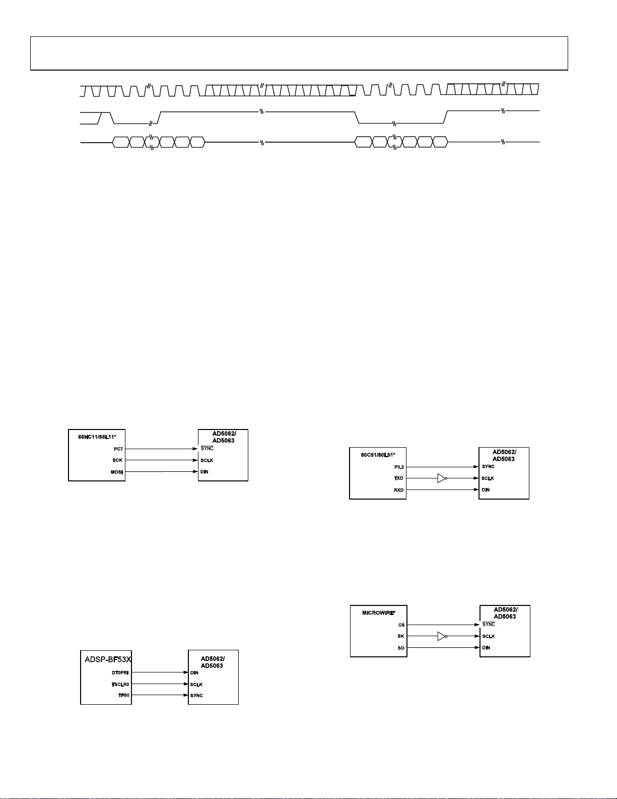
TIMING CHARACTERISTICS
(VDD = 2.7-5.5 V; all specifications T
Parameter Limit1 Unit Test Conditions/Comments
3
t
1
t2
t3
t4
t5
t6
t7
t8
t9
NOTES
1
All input signals are specified with tr = tf = 1 ns/V (10% to 90% of VDD) and timed from a voltage level of (VIL + VIH)/2.
2
See Figure 1.
3
Maximum SCLK frequency is 30 MHz.
Specifications subject to change without notice.
to T
MIN
unless otherwise noted)
MAX
33 ns min SCLK Cycle Time
13 ns min SCLK High Time
12 ns min SCLK Low Time
13 ns min
SYNC to SCLK Falling Edge Setup Time
5 ns min Data Setup Time
4.5 ns min Data Hold Time
0 ns min
33 ns min
13 ns min
SCLK Falling Edge to SYNC Rising Edge
Minimum SYNC High Time
SYNC Rising Edge to next SCLK Fall
Ignore
.
Figure 1. Timing Diagram
Rev. Pr C | Page 4 of 19
Preliminary Technical Data AD5062/AD5603
ABSOLUTE MAXIMUM RATINGS
Table 1. Absolute Maximum Ratings (TA = 25°C unless otherwise noted)
Parameter Rating
VDD to GND –0.3 V to + 7.0 V
Digital Input Voltage to GND –0.3 V to VDD + 0.3 V
V
to GND1 –0.3 V to VDD + 0.3 V
OUT
Operating Temperature Range
Industrial (B Version) –40°C to +125°C
Storage Temperature Range –65°C to +150°C
Maximum Junction Temperature 150°C
SOT23 Package
Power Dissipation (Tj Max-Ta)/ θJA
θJA Thermal Impedance 240°C/W
Lead Temperature, Soldering
Vapour Phase (60 Sec) 215°C
Infrared (15 Sec) 220°C
uSOIC Package
θJA Thermal Impedance 206°C/W
θJc Thermal Impedance 44°C/W
Lead Temperature, Soldering
Vapour Phase (60 Sec) 215°C
Infrared (15 Sec) 220°C
Stresses above those listed under Absolute Maximum Ratings may cause permanent damage to the device. This is a stress rating only;
functional operation of the device at these or any other conditions above those listed in the operational sections of this specification is not
implied. Exposure to absolute maximum rating conditions for extended periods may affect device reliability.
ESD Caution
ESD (electrostatic discharge) sensitive device. Electrostatic charges as high as 4000 V readily accumulate on
the human body and test equipment and can discharge without detection. Although this product features
proprietary ESD protection circuitry, permanent damage may occur on devices subjected to high energy
electrostatic discharges. Therefore, proper ESD precautions are recommended to avoid performance
degradation or loss of functionality.
This device is a high performance RF integrated circuit with an ESD rating of <2 kV, and it is ESD sensitive. Proper precautions should be
taken for handling and assembly.
Rev. Pr C | Page 5 of 19

AD5062/AD5063 Preliminary Technical Data
Model Temperature
Range
AD5062BRJ-1 -40OC to 125 OC 1 LSB 2.7-5.5V, Reset to Zero RT8
AD5062BRJ-1500RL7 -40OC to 125 OC 1 LSB 2.7-5.5V, Reset to Zero RT8
AD5062BRJ-1REEL7 -40OC to 125 OC 1 LSB 2.7-5.5V, Reset to Zero RT8
AD5062BRJ-2 -40OC to 125 OC 1 LSB 2.7-5.5V, Reset to Mid RT8
AD5062BRJ-2500RL7 -40OC to 125 OC 1 LSB 2.7-5.5V, Reset to Mid RT8
AD5062BRJ-2 REEL7 -40OC to 125 OC 1 LSB 2.7-5.5V, Reset to Mid RT8
AD5062BRJ-3 -40OC to 125 OC 2 LSB 2.7-5.5V, Reset to Zero RT8
AD5062EB -40OC to 125 OC AD5062 Evaluation
AD5063BRM-1 -40OC to 125 OC 1 LSB 2.7-5.5V, Reset to Zero RM-10
INL Description Package
Options
Board
Rev. Pr C | Page 6 of 19
Preliminary Technical Data AD5062/AD5063
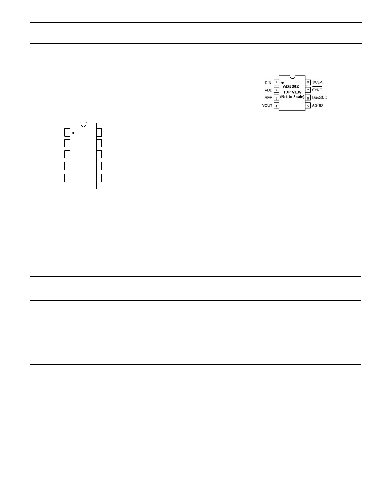
PIN CONFIGURATION AND FUNCTION
DESCRIPTION
1
DIN
V
REF
V
INV
Figure 3. AD5063 10 ld uSOIC.
Table 2. Pin Function Descriptions
DD
OUT
AD5063
2
TOP VIEW
(Not to Scale)
3
4
5
Mnemonic Function
VDD Power Supply Input. These parts can be operated from +2.5 V to +5.5 V and VDD should be decoupled to GND.
REF Reference Voltage Input.
DacGND Ground input to the DAC.
V
OUT
Analog output voltage from DAC.
Level triggered control input (active low). This is the frame synchronization signal for the input data. When SYNC goes low,
SYNC
it enables the input shift register and data is transferred in on the falling edges of the following clocks. The DAC is updated
following the 16th clock cycle unless SYNC is taken high before this edge in which case the rising edge of SYNC acts as an
interrupt and the write sequence is ignored by the DAC.
SCLK
DIN
Serial Clock Input. Data is clocked into the input shift register on the falling edge of the serial clock input. Data can be
transferred at rates up to 30 MHz.
Serial Data Input. This device has a 24 bit shift register. Data is clocked into the register on the falling edge of the serial clock
input.
AGND Ground reference point for Analog circuitry on the part.
RFB Feedback Resistor. In bipolar mode connect this pin to external op amp circuit.
INV Connected to the internal Scaling resistors of the DAC. Connect INV pin to external op-amps inverting input in bipolar mode.
10
SCLK
SYNC
9
DacGND
8
AGND
7
6
RFB
Figure 2. AD5062 8ld Sot23
Rev. Pr C | Page 7 of 19

AD5062/AD5063 Preliminary Technical Data
Rev. Pr C | Page 8 of 19

Preliminary Technical Data AD5062/AD5063
Gain Error
TERMINOLOGY
Relative Accuracy
For the DAC, relative accuracy or Integral Nonlinearity (INL)
is a measure of the maximum deviation, in LSBs, from a straight l in e
passing through the endpoints of the DAC transfer function. A
typical INL vs. code plot can be seen in Figure 2.
Differential Nonlinearity
Differential Nonlinearity (DNL) is the difference between the
measured change and the ideal 1 LSB change between any two
adjacent codes. A specified differential nonlinearity of ±1 LSB
maximum ensures monotonicity. This DAC is
guarantee d monotonic by design. A typical DNL vs. code plot
can be seen in Figure 3.
Zero-Code Error
Zero-code error is a measure of the output error when zero
code (0000Hex) is loaded to the DAC register. Ideally the
output should be 0 V. The zero-code error is always positive in
the AD5062/AD5063 because the output of the DAC cannot go
below 0 V. It is due to a combination of the offset errors in the
DAC and output amplifier. Zero-code error is expressed in mV.
A plot of zero-code error vs. temperature can be seen in Figure
6.
Full-Scale Error
Full-scale error is a measure of the output error when full-scale
code (FFFF Hex) is loaded to the DAC register. Ideally the
output should be VDD – 1 LSB. Full-scale error is expressed in
percent of full-scale range. A plot of full-scale error vs.
temperature can be seen in Figure 6.
This is a measure of the span error of the DAC. It is the
deviation in slope of the DAC transfer characteristic from ideal
expressed as a percent of the full-scale range.
Total Unadjusted Error
Total Unadjusted Error (TUE) is a measure of the output error
taking all the various errors into account. A typical TUE vs.
code plot can be seen in Figure 4.
Zero-Code Error Drift
This is a measure of the change in zero-code error
with a change in temperature. It is expressed in µV/°C.
Gain Error Drift
This is a measure of the change in gain error with changes in
temperature. It is expressed in (ppm of full-scale range)/°C.
Digital-to-Analog Glitch Impulse
Digital-to-analog glitch impulse is the impulse injected into the
analog output when the input code in the DAC register changes
state. It is normally specified as the area of the glitch in nV secs
and is measured when the digital input code is
changed by
1 LSB at the major carry transition (7FFF Hex to 8000 Hex). See
Figure 19.
Digital Feedthrough
Digital feedthrough is a measure of the impulse injected into
the analog output of the DAC from the digital inputs of the
DAC but is measured when the DAC output is not updated. It
is specified in nV secs and measured with a full-scale
code change on the data bus, i.e., from all 0s to all 1s and vice
versa.
Rev. Pr C | Page 9 of 19
AD5062/AD5063 Preliminary Technical Data
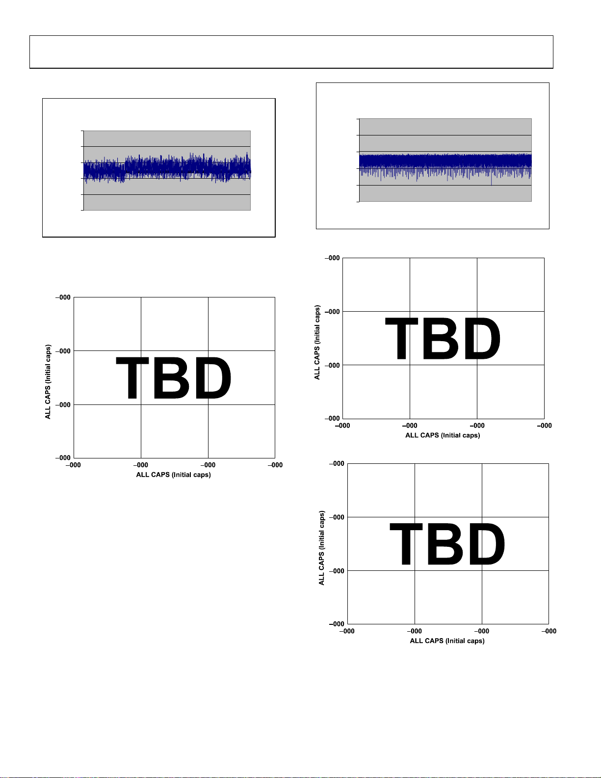
INL Line ar ity Plot
1
1
0.6
0.2
LSB
-0.2
-0.6
-1
DAC Code
Figure 4. Typical INL Plot
LSB
0.6
0.2
-0.2
-0.6
-1
DNL Linearity Plot
DAC Code
Figure 6. Typical DNL Plot.
Figure 5. Zero Scale Error and Full Scale Error vs. Temperature
Figure 7. INL & DNL vs Supply
Figure 8. Idd Histogram @ Vdd=3/5 Volts.
Rev. Pr C | Page 10 of 19

Preliminary Technical Data AD5062/AD5063
Figure 9. Supply Current vs. Temperature
Figure 12. Supply Current vs Supply Voltage
Figure 10. Full Scale Settling Time
Figure 13. Half Scale Settling Time
Figure 11. Supply Current vs Code.
Rev. Pr C | Page 11 of 19
Figure 14. Power on Reset to 0 Volts.
AD5062/AD5063 Preliminary Technical Data
Figure 15. Digital to Analog Glitch Impulse
Figure 16. Output Spectral Density 100k Bandwidth
Figure 18. Harmonic Distortion on digitally Generated Waveform.
Figure 19. 0.1 Hz to 10 Hz Noise Plot
Figure 17. Exiting Power-Down
Figure 20. PowerUp Transient
Rev. Pr C | Page 12 of 19
Preliminary Technical Data AD5062/AD5063
Figure 21. Glitch Energy
Figure 22. Offset Error Distribution
Figure 23. Gain Error Distribution
Rev. Pr C | Page 13 of 19

AD5062/AD5063 Preliminary Technical Data
GENERAL DESCRIPTION
The AD5062/AD5063 are single 16-bit, serial input, voltage
output DACs. It operates from supply voltages of 2.7-5.5 V. Data
is written to the AD5062/63 in a 24-bit word format, via a 3wire serial interface
The AD5062/AD5063 incorporates a power-on reset circuit,
which ensures that the DAC output powers up to 0 V or midscale. The device also has a software power-down mode pin,
which reduces the typical current consumption to XX.
DAC Architecture
The DAC architecture of the AD5062/AD5063 consists of two
matched DAC sections. A simplifed circuit diagram is shown in
Figure X The four MSBs of the 16-bit data word are decoded to
drive 15 switches, E1 to E15. Each of these switches connects
one of 15 matched resistors to either AGND or VREF. The
remaining 12 bits of thedata word drive switches S0 to S11 of a
12-bit voltage modeR-2R ladder network.
buffered reference for the DAC core
SERIAL INTERFACE
The AD5062/AD5063 have a three-wire serial
interface (SYNC, SCLK and DIN), which is
compatible with SPI, QSPI and MICROWIRE interface
standards as well as most DSPs. See Figure 1 for a timing
diagram of a typical write sequence.
The write sequence begins by bringing the SYNC line low.
Data from the DIN line is clocked into the 24-bit shift register
on the falling edge of SCLK. The serial clock frequency can be
as high as 30 MHz, making these parts compatible with high
speed DSPs. On the 24th falling clock edge, the last data bit is
clocked in and the programmed function is executed (i.e., a
change in DAC register contents and/or a change in the mode
of operation). At this stage, the SYNC line may be kept low or
be brought high. In either case, it must be brought high for a
minimum of 33 ns before the next write sequence so that a
falling edge of SYNC can initiate the next write sequence. Since
the SYNC buffer draws more current when VIN = 1.8 V than it
does when VIN = 0.8 V, SYNC should be idled low between
write sequences for even lower power operation of the part. As
is mentioned above, however, it must be brought high again
just before the next write sequence.
Figure X. DAC Ladder Structure
Reference Buffer
The AD5062/AD5063 operates with an external reference.
The reference input (REFIN) has an input range of up to
4.096 V. This input voltage is then used to provide a
Figure 22. Input Register Contents
Input Shift Register
The input shift register is 24 bits wide (see Figure 22). Bit D22
is the Reset Reg bit. When this is enabled the data will be loaded
into the Reset Register. This will remain the reset code until the
part powers down. D21, D20 are control bits that control
which mode of operation the part is in (normal mode or any
one of three power-down modes). There is a more complete
description of the v ar i o u s modes in t h e Power-Down
Modes section. The next twenty bits are the data bits. These are
tr an sf erred to the DAC register on the 24th falling edge of SCLK.
Rev. Pr C | Page 14 of 19

Preliminary Technical Data AD5062/AD5063
SYNC Interrupt
In a normal write sequence, the SYNC line is kept low for at
least 24 falling edges of SCLK and the DAC is updated on the
24th falling edge. However, if SYNC is brought high before the
24th falling edge this acts as an interrupt to the write sequence.
The shift register is reset and the write sequence is
seen as invalid. Neither an update of the DAC register
contents or a change in the operating mode occurs—see Figure
23.
Power-On-Reset
The AD5062/AD5063 contains a power-on-reset circuit that
controls the output voltage during power-up. The DAC register
is filled with zeros and the output voltage is 0 V. It remains
there until a valid write sequence is made to the DAC. This is
useful in applications where it is important to know the state of
the output of the DAC while it is in the process of powering up.
Software Reset.
The AD5062/AD5063 can be put into software reset by setting
all in the Dac register to one. For the AD5060 this includes
writing ones to bits D23-D16, which in not the normal mode of
operation. Note: The
performed if a software reset command is started.
SYNC Interrupt command cannot be
Power-Down Modes
The AD5062/AD5063 contains four separate modes of
operation. These modes are software-programmable by setting
two bits (DB17 and DB16) in the control register. Table I shows
how the state of the bits corresponds to the mode of operation
of the device.
Table I. Modes of Operation for the
AD5062/AD5063
DB15 DB14 Operating Mode
0 0 Normal Operation
Power-Down Mode
0 1 TRI-STATE
1 0 100 kΩ to GND
1 1 1 kΩ to GND
When both bits are set to 0, the part works normally with its
normal power consumption. However, for the three power-
down modes, the supply current falls to 200 nA at 5 V (50 nA at
3 V). Not only does the supply c u r r ent fall b u t t h e
output stage is also internally switched from the output of
the amplifier to a resistor network of kn o w n v a l ues. T h i s
has the advantage that th e o u t put imp e d a n c e of the p a r t
is known while the part is in power-down mode.
There are three different options. The output is
c o n nected internally to GND through a 1kΩ resistor, a 100 kΩ resistor
or it is left open-circuited (Three-State). The output stage is illustrated in
Figure 24.
Figure 24. Output Stage During Power-Down
The bias generator, the output amplifier, the resistor string and
other associated linear circuitry are all shut down
when the power-down mode is activated. However, the
contents of the DAC register are unaffected when in powerdown. The time to exit power-down is typically 2.5 µs for VDD
= 5 V and 5 µs for VDD = 3 V. See Figure 18 for a plot.
MICROPROCESSOR INTERFACING
AD5062/AD5063 to ADSP-2101/ADSP-2103
Interface
Figure 25 shows a serial interface between the AD5062/AD5063
and the ADSP-2101/ADSP-2103. The ADSP-2101/ADSP-2103
should be set up to operate in the SPORT Transmit Alternate
Framing Mode. The ADSP-2101/ADSP-2103 SPORT is
programmed through the SPORT control register and should
be configured as follows: Internal Clock Operation, Active Low
Framing, 16-Bit Word Length. Transmission is initiated by
writing a word to the Tx registe r a f t e r the SPORT h a s
been enabled.
Figure 25. AD5062/AD5063 to ADSP-2101/ADSP-2103
Interface
Rev. Pr C | Page 15 of 19
AD5062/AD5063 Preliminary Technical Data
SCLK
SYNC
DIN
DB23
INVALID WRITE SEQUENCE:
SYNC HIGH BEFORE 24TH FALLING EDGE
DB0
Figure 23. SYNC Interrupt Facility
AD5062/AD5063 to 68HC11/68L11 Interface
Figure 26 shows a serial interface between the AD5060 and the
68HC11/68L11 microcontroller. SCK of the 68HC11/68L11
drives the SCLK of the AD5060, while the MOSI
output drives the serial data line of the DAC. The SYNC
signal is derived from a port line (PC7). The setup conditions
for correct operation of this interface are as follows: the
68HC11/68L11 should be configured so that its CPOL bit is a 0
and its CPHA bit is a 1. When data is being transmitted
to the DAC, t h e SYNC line is taken low (PC7). When the
68HC11/68L11 is configured as above, data appearing on the
MOSI output is valid on the falling edge of SCK. Serial data
from the 68HC11/68L11 is transmitted in 8-bit bytes with only
eight falling clock edges occurring in the transmit cycle. Data is
transmitted MSB first. In order to load data to the
AD5062/AD5063, PC7 is left low after the first eight bits are
transferred, and a second serial write operation is performed to
the DAC and PC7 is taken high at the end of this procedure.
DB23
VALID WRITE SEQUENCE, OUTPUT UPDATES
ON THE 24
TH
FALLING EDGE
DB0
AD5062/AD5063 to 80C51/80L51 Interface
Figure 27 shows a serial interface between the AD5062/AD5063
and the 80C51/80L51 microcontroller. The setup for the
inter fa ce i s as follows: TXD of the 80C51/80L51 drives SCLK of the
AD5062/AD5063, while RXD drives the serial data line of the
part. The SYNC signal is again derived from a bit
programmable pin on the port. In this case port line P3.3 is
used. When data is to be transmitted to the AD5062/AD5063,
P3.3 is taken low. The 80C51/80L51 transmits data only in 8-bit
bytes; thus only eight falling clock edges occur in the transmit
cycle. To load data to the DAC, P3.3 is left low after the first
eight bits are transmitted, and a second write cycle is initiated
to transmit the second byte of data. P3.3 is taken high following
the completion of this cycle. The 80C51/80L51 outputs the
serial data in a format which has the LSB first. The
AD5062/AD5063 requires its data with the MSB as the first bit
received. The 80C51/80L51 transmit routine should take this
into account.
Figure 26. AD5062/AD5063 to 68HC11/68L11 Interface
AD5062/AD5063 to Blackfin ADSP-BF53X
Interface
Figure 2X shows a serial interface between the AD5641 and the
Blackfin ADSP-53X microprocessor. The ADSP-BF53X processor
family incorporates two dual-channel synchronous serial ports,
SPORT1 and SPORT0 for serial and multiprocessor
communications. Using SPORT0 to connect to the AD5062/63, the
setup for the interface is as follows. DT0PRI drives the SDIN pin of
the AD5062/63, while TSCLK0 drives the SCLK of the part. The
SYNC is driven from TFS0.
Figure 2X. AD5062/AD5063 to Blackfin ADSP-BF53X
Interface
Rev. Pr C | Page 16 of 19
Figure 27. AD5062/AD5063 to 80C51/80L51 Interface
AD5062/AD5063 to Microwire Interface
Figure 28 shows an interface between the AD5062/AD5063 and
any microwire compatible device. Serial data is shifted out on
the falling edge of the serial clock and is clocked into the
AD5062/AD5063 on the rising edge of the SK.
Figure 28. AD5062/AD5063 to MICROWIRE Interface
APPLICATIONS
Choosing a Reference for the AD5062/AD5063.
To achieve the optimum performance from the AD5060,
thought should be given to the choice of a precision voltage

Preliminary Technical Data AD5062/AD5063
⎣
⎝
⎠
6
V
reference. The AD5062/AD5063 have just one reference input,
REFIN. The voltage on the reference input is used to supply the
positive input to the Dac . Therefore any error in the reference
will be reflected in the Dac.
There are 4 possible sources of error when choosing a voltage
reference for high accuracy applications; initial accuracy, ppm
drift, long term drift and output voltage noise. Initial accuracy
on the output voltage of the Dac will lead to a full scale error in
the Dac. To minimize these errors, a reference with high initial
accuracy is preferred. Also, choosing a reference with an output
trim adjustment, such as the ADR423 allow a system designer
to trim system errors out by setting a reference voltage to a
voltage other than the nominal. The trim adjustment can also
be used at temperature to trim out any error.
5V
3.01v
AD5062/3
V
=0VTO3.01V
OUT
THREE-WIRE
SERIAL
INTERFACE
ADR423
SYNC
SCLK
DIN
Figure 29. ADR423 as Reference to AD5062/AD5063
Long term drift is a measure of how much the reference drifts
over time. A reference with a tight long term drift specification
ensures that the overall solution remains relatively stable
during its entire lifetime.
The temperature co-efficient of a references output voltage
affect INL,DNL TUE. A reference with a tight temperature coefficient specification should be chosen to reduce temperatue
dependence of the Dac output voltage on ambient conditions.
In high accuracy applications, which have a relatively low
noise budget, reference output voltage noise needs to be
considered. Choosing a reference with as low an output noise
voltage as practical for the system noise resolution required is
important. Precision voltage references such as the ADR435
produce low output noise in the 0.1-10Hz region. Examples of
some recommended precision references for use as supply to
the AD5060 are shown in the figure below..
Part list of precision references for use with
AD5062/AD5063.
Part No.
Initial
Accuracy
(mV max)
Temp Drift
o
(ppm
C max)
0.1-10Hz Noise
(uV p-p typ)
ADR435 +/-6 3 3.4
ADR425 +/-6 3 3.4
ADR02 +/-5 3 15
ADR395 +/-6 25 5
Bipolar Operation Using the AD5062/AD5063
The AD5062/AD5063 has been designed for single-supply
operation but a bipolar output range is also possible using the
circuit in Figure 30. The circuit below will give an output
voltage range of ±4.096 V. Rail-to-rail operation at the
amplifier output is achievable using an AD820 or an OP295 as
the output amplifier.
The output voltage for any input code can be calculated as
follows:
⎡
=
V
O
×
⎜
V
DD
⎢
65536
⎝
⎛
⎢
⎛
⎞
⎟
×
⎠
R1+R2
⎜
⎝
D
R1
⎞
⎟
V
DD
⎠
⎤
⎛
⎞
R2
⎥
×
⎟
⎜
⎥
R1
⎝
⎠
⎦
where D represents the input code in decimal (0–16384).
With V
V
O
= 5 V, R1 = R2 = 10 kW:
REF
10×D
65536
⎞
5V
⎟
⎛
=
⎜
This is an output voltage range of ±5 V with 0000Hex
corresponding to a –5 V output and 3FFF Hex
corresponding to a +5 V output.
+4.09
10uF
0.1uF
REF
AD5063
AGND
RFB
R
FB
INV
R
INV
OUT
+5V
–5V
EXTERNAL
OP AMP
BIPOLAR
OUTPUT
SERIAL
INTERFACE
0.1uF
+5V
V
DD
SYNC
DIN
SCLK
DacGND
Figure 30. Bipolar Operation with the AD5063
Using AD5062/AD5063 with an Opto-Isolated
Interface Chip.
In process-control applications in industrial environments it is
often necessary to use an opto-isolated interface to protect and
isolate the controlling circuitry from any hazardous commonmode voltages that may occur in the area where the DAC is
functioning. Because the AD5062/AD5063 uses a three-wire
serial logic interface, the ADuM130Xifamily s an ideal way to
provide digital isolation for the DAC interface.
The ADuM130x isolators provide three independent isolation
channels in a variety of channel configurations and data rates.
Rev. Pr C | Page 17 of 19

AD5062/AD5063 Preliminary Technical Data
They operate across the full range from 2.7V to 5.5V, providing
compatibility with lower voltage systems as well as enabling a
voltage translation functionality across the isolation barrier.
Figure 31. The power supply to the part also needs to be
isolated. This is done by using a transformer. On the DAC side
of the transformer, a +5 V regulator provides the +5 V supply
required for the AD5062/AD5063.
+5V
SCLK
SDI
DATA
POWER
V1A
V1B
V1C
ADMu103x
VOA
VOB
VOC
REGULATOR
SCLK
SDI
DIN
V
DAC
GND
DD
10. F
0.1. F
V
OUT
Figure 31. AD5062/AD5063 with An Opto-Isolated Interface
Power Supply Bypassing and Grounding
When accuracy is important in a circuit it is helpful to carefully
consider the power supply and ground return layout on the
board. The printed circuit board containing the
AD5062/AD5063 should have separate analog and digital
sections, each having its own area of the board. If the
AD5062/AD5063 is in a system where other devices require an
AGND to DGND connection, the connection sh o u l d b e
made at one point only. This ground point should be
as close as possible to the AD5062/AD5063.
The power supply to the AD5062/AD5063 should be
bypassed with
10 µF and 0.1 µF capacitors. The capacitors should be
physically as close as possible to the device with the 0.1 µF
capacitor ideally right up against the device. The 10 µF
capacitors are the tantalum bead type. It is important that the
0.1 µF capacitor has low Effective Series Resistance (ESR) and
Effective Series Inductance (ESI), e.g., common ceramic types
of capacitors. This 0.1 µF capacitor provides a low impedance
path to ground for high frequencies caused by transient
currents due to internal logic switching.
The power supply line itself should have as large a trace as
possible to provide a low impedance path and reduce glitch
effects on the supply line. Clocks and other fast switching
digital signals should be shielded from other parts of
the board b y d i gital ground. Avoid crossover of digital and
analog signals if possible. When traces cross on opposite sides
of the board, ensure that they run at right angles to each other
to reduce feedthrough effects through the board. The best
board layout technique is the microstrip technique where the
component side of the board is dedicated to the ground plane
only and the signal traces are placed on the solder side.
However, this is not always possible with a two-layer board.
Rev. Pr C | Page 18 of 19
Preliminary Technical Data AD5062/AD5063
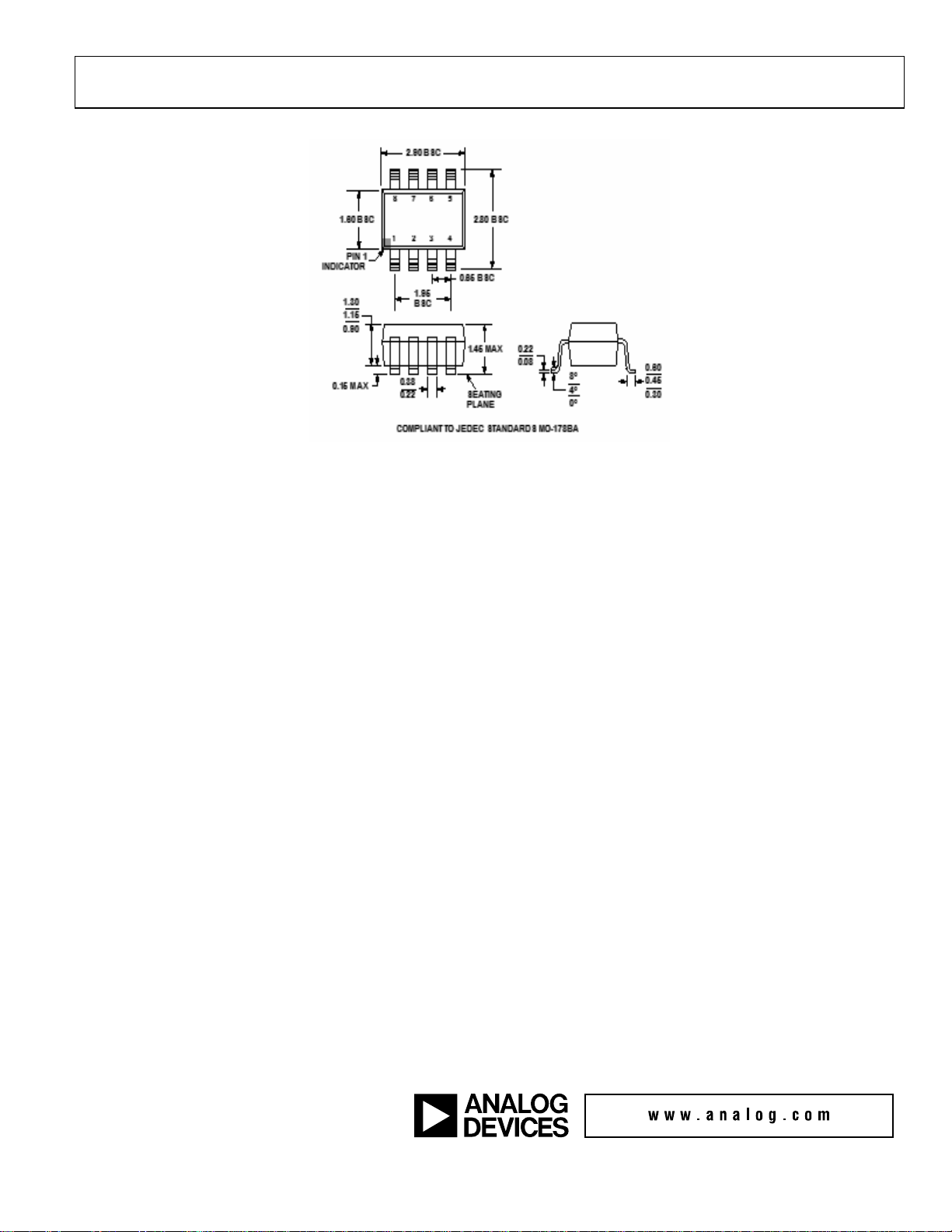
8 ld SOT23
Outline Dimensions
Dimensions shown in inches and mms
© 2005 Analog Devices, Inc. All rights reserved. Trademarks and
registered trademarks are the property of their respective owner.
PR04766-0-1/05(PrC).
 Loading...