查询AD12401供应商
FEATURES
Dual op amp
Voltage feedback
Wide supply range: from 3.3 V to 24 V
Rail-to-rail output
Output swing to within 0.5 V of supply rails @ 230 mA
23 V p-p differential, R
High output current
Linear output current of 230 mA peak into 25 Ω
−68 dBc MTPR @ 15 dBm (100 Ω telephone line)
Low noise
4.5 nV/√Hz voltage noise density @ 100 kHz
1.5 pA/√Hz current noise density @ 100 kHz
High speed
65 MHz bandwidth (A
55 V/μs slew rate (R
APPLICATIONS
Consumer xDSL modems
Twisted pair line drivers
ADSL CPE applications
(Drop in replacement for TS613ID and EL1519CS)
Audio applications
GENERAL DESCRIPTION
of 50 Ω from 12 V supply
LOAD
= 1, −3 dB)
V
= 25 Ω)
LOAD
Rail-to-Rail Upstream ADSL Line Driver
AD45048
PIN CONFIGURATION
OUT1
1
–IN1
2
+IN1
3
4
–V
S
Figure 1. 8-Lead SOIC
10
0
–10
–20
–30
–40
dBm
–50
–60
–70
–80
–90
CENTER 86.31174378kHz 1kHz/ SPAN 10kHz
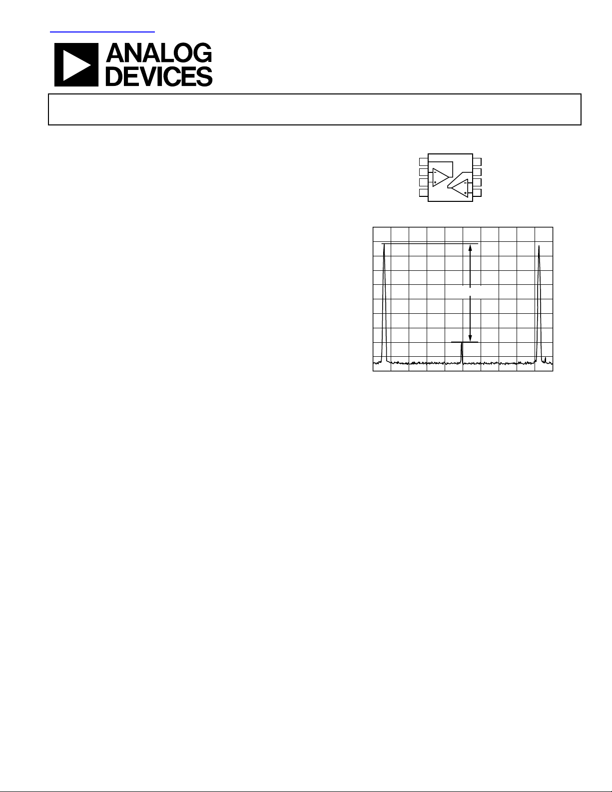
Figure 2. AD45048AR Upstream ADSL MTPR (13 dBm, CF = 5.3)
–68dB
+V
8
S
OUT2
7
6
–IN2
5
+IN2
04817-Sp0-001
04817-Sp0-002
The AD45048 ADSL CPE line driver is a dual operational
amplifier capable of driving high output current (230 mA); it
features a rail-to-rail output stage that swings to within 0.5 V
of the supply rails. The AD45048 rail-to-rail output stage
surpasses the output voltage capability of typical emitterfollower output stages and can deliver up to 23 V p-p
differentially from a single 12 V supply in ADSL CPE line
driving applications. The low distortion, high output current
and wide output dynamic range make the AD45048 ideal for
driving upstream signals in ADSL CPE applications.
Fabricated with ADI’s high speed XFCB-HV (eXtra Fast
Complementary Bipolar-High Voltage) process, the high
bandwidth and fast slew rate of the AD45048 keep distortion to
a minimum while dissipating minimum power. The AD45048 is
available in a standard 8-lead SOIC package that can operate
from −40°C to +85°C.
Rev. A
Information furnished by Analog Devices is believed to be accurate and reliable. However, no
responsibility is assumed by Anal og Devices for its use, nor for any infringements of patents or ot her
rights of third parties that may result from its use. Specifications subject to change without notice. No
license is granted by implication or otherwise under any patent or patent rights of Analog Devices.
Trademarks and registered trademarks are the property of their respective owners.
One Technology Way, P.O. Box 9106, Norwood, MA 02062-9106, U.S.A.
Tel: 781.329.4700 www.analog.com
Fax: 781.461.3113 © 2005 Analog Devices, Inc. All rights reserved.

AD45048
TABLE OF CONTENTS
Features.............................................................................................. 1
General Description..........................................................................7
Applications....................................................................................... 1
General Description......................................................................... 1
Pin Configuration............................................................................. 1
Revision History ............................................................................... 2
Specifications..................................................................................... 3
Absolute Maximum Ratings............................................................ 4
ESD Caution.................................................................................. 4
Typical Performance Characteristics............................................. 5
REVISION HISTORY
9/05—Rev. 0 to Rev. A
Updated Outline Dimensions......................................................... 8
Changes to Ordering Guide............................................................ 8
7/04—Revision 0: Initial Version
Power Supply and Decoupling.....................................................7
Layout Considerations..................................................................7
CPE ADSL Application ................................................................7
Transformer Selection ..................................................................7
Receive Channel Considerations.................................................7
Outline Dimensions..........................................................................8
Ordering Guide .............................................................................8
Rev. A | Page 2 of 8

AD45048
SPECIFICATIONS
VS = ±6 V or +12 V (@ TA = 25°C, G = +10, RL = 100 Ω, unless otherwise noted).
Table 1.
Parameter Test Conditions/Comments Min Typ Max Unit
DYNAMIC PERFORMANCE
−3 dB Bandwidth G = +1, V
0.1 dB Flatness V
Large Signal Bandwidth V
Large Signal Slew Rate V
OUT
OUT
OUT
NOISE/DISTORTION PERFORMANCE
Distortion (Worst Harmonic) fC = 40 kHz, V
Multitone Power Ratio 26 kHz to 134 kHz, Z
Input Voltage Noise f = 100 kHz 4.5 nV/√Hz
Input Current Noise f = 100 kHz 1.5 pA/√Hz
DC PERFORMANCE
Input Offset Voltage 1 2.5 mV
T
MIN
Input Offset Voltage Match 1 2.0 mV
Input Bias Current 200 900 nA
T
MIN
Input Offset Current 50 300 nA
Open-Loop Gain 85 94 dB
INPUT CHARACTERISTICS
Input Resistance f = 100 kHz 87 kΩ
Input Capacitance 1.4 pF
OUTPUT CHARACTERISTICS
Output Resistance 1.4 MHz; G = +1 0.2 Ω
Output Voltage Swing Maximum swing (differential) V
Minimum swing (differential) V
Differential Output Voltage Swing ΔV
Single-Ended +Swing R
Single-Ended -Swing R
Single-Ended +Swing R
Single-Ended –Swing R
OUT
LOAD
LOAD
LOAD
LOAD
Operating Range (Dual Supply) ±1.5 ±12.6 V
Supply Current 7 9 12 mA
Power Supply Rejection Ratio ±0.5 V −85 −75 dB
Common-Mode Rejection Ratio ±1 V −86 −79 dB
= 0.1 V p-p, RFB = 0 Ω, R
OUT
= 0.1 V p-p single-ended, G = +1, R
= 1 V p-p single-ended, G = +10, R
= 5 V p-p, G = +1, R
= 6 V p-p, single-ended, R
OUT
− T
2.5 mV
MAX
− T
1.3 μA
MAX
= V
− V
OMAX
OMIN
= 25 Ω 55 V/μs
LOAD
= 100 Ω, XFMR = 1:2 turns, P
LINE
22.5 23 V p-p
= 25 Ω 65 MHz
LOAD
= 25 Ω 3.35 MHz
LOAD
= 25 Ω 4.5 MHz
LOAD
= 25 Ω −80 dBc
LOAD
= 13 dBm −68 dBc
LINE
, R
OMAX
OMIN
= 50 Ω differential 11.25 11.5 V diff
LOAD
, R
= 50 Ω differential −11.5 −11.25 V diff
LOAD
= 25 Ω 5.68 5.76 Vp
= 25 Ω −5.67 −5.58 Vp
= 100 Ω 5.92 5.95 Vp
= 100 Ω −5.91 −5.86 Vp
Rev. A | Page 3 of 8
 Loading...