Analog Devices AD394 a Datasheet

µP-Compatible Multiplying
FEATURES
Four, complete, 12-bit CMOS DACs with buffer registers
, T
Linearity error: ±1/2 LSB T
Factory-trimmed gain and offset
Precision output amplifiers for V
Full four-quadrant multiplication per DAC
Monoticity guaranteed over full temperature range
Fast settling: 15 µs maximum to ±1/2 LSB
Available in MIL-STD-883B
MIN
PRODUCT DESCRIPTION
The AD394 contains four 12-bit, high-speed, low power, voltage
output, multiplying digital-to-analog converters in a compact
28-pin hybrid package. The design is based on a proprietary,
latched, 12-bit, CMOS DAC chip, which reduces chip count and
provides high reliability. The AD394 is ideal for systems
requiring digital control of many analog voltages where board
space is at a premium and low power consumption is a necessity. Such applications include automatic test equipment, process
controllers, and vector stroke displays.
(AD394T)
MAX
OUT
Quad 12-Bit D/A Converter
AD394
The AD394 is laser-trimmed to ±1/2 LSB maximum differential
and integral linearity (AD394T) and full-scale accuracy of
±0.05 percent at 25°C. The high initial accuracy is possible
because of the use of precision, laser-trimmed, thin-film scaling
resistors.
CS1
The individual DAC registers are accessed by the
CS4
control pins. These control signals allow any combination
through
of the DAC select matrix to occur (see Table 3). Once selected,
the DAC is loaded with a single 12-bit wide word. The 12-bit
parallel digital input interfaces to most 12- and 16-bit bus
systems.
The AD394 outputs (V
= 10 V) provide a ±10 V bipolar
REFIN
output range with positive-true offset binary input coding.
The AD394 is packaged in a 28-lead ceramic package and is
available for operation over a −55°C to +125°C temperature
range.
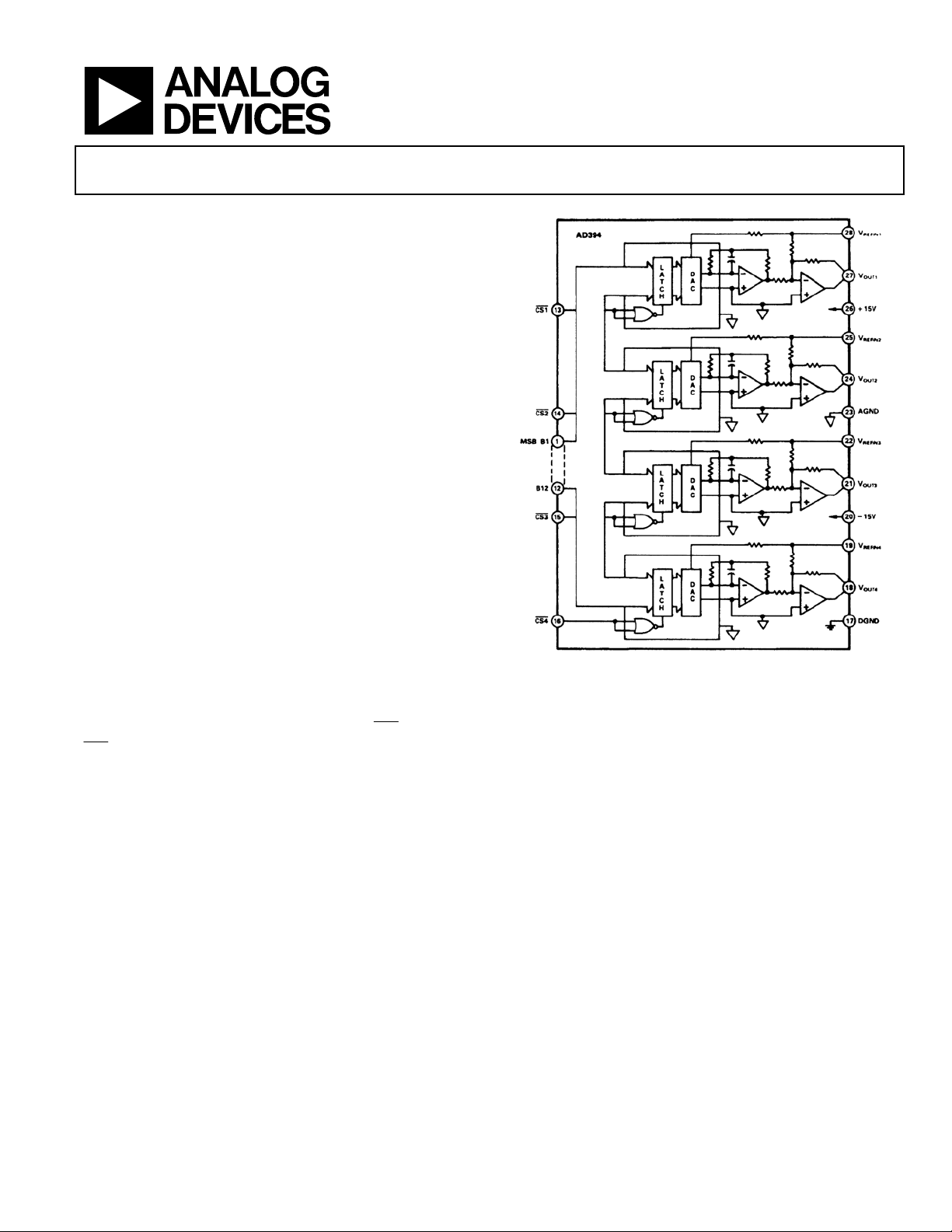
Figure 1. Functional Block Diagram
PRODUCT HIGHLIGHTS
1. The AD394 offers a dramatic reduction in printed circuit
board space in systems using multiple low power DACs.
2. Each DAC is independently addressable and provides
versatile control architecture for a simple interface to
microprocessors. All latch enable signals are leveltriggered.
3. The output voltage is trimmed to a full-scale accuracy of
±0.05%. Settling time to ±1/2 LSB is 15 µs maximum.
4. A maximum gain TC of 5 ppm/°C is achievable.
5. Two- or four-quadrant multiplication can be achieved
simply by applying the appropriate input voltage signal to
the selected DAC's reference (V
6. The AD394TD features guaranteed accuracy and linearity
over the −55°C to +125°C temperature range.
REFIN
).
Rev. A
Information furnished by Analog Devices is believed to be accurate and reliable.
However, no responsibility is assumed by Analog Devices for its use, nor for any
infringements of patents or other rights of third parties that may result from its use.
Specifications subject to change without notice. No license is granted by implication
or otherwise under any patent or patent rights of Analog Devices. Trademarks and
registered trademarks are the property of their respective owners.
One Technology Way, P.O. Box 9106, Norwood, MA 02062-9106, U.S.A.
Tel: 781.329.4700
Fax: 781.326.8703 © 2004 Analog Devices, Inc. All rights reserved.
www.analog.com

AD394
TABLE OF CONTENTS
Specifications..................................................................................... 3
Analog Circuit Details ..................................................................8
Absolute Maximum Ratings............................................................ 5
ESD Caution.................................................................................. 5
Pin Configuration and Functional Block Diagram...................... 6
Theory of Operation ........................................................................ 7
Multiplying Mode ......................................................................... 7
Data and Control Signal Format ................................................7
Timing............................................................................................ 8
REVISION HISTORY
9/04–Rev. 0 Changed to Rev. A
Updated format....................................................................... Universal
Deleted AD395 part................................................................ Universal
Change to Product Description...........................................................1
Changes to Specifications table............................................................3
Delete Figure 3 .......................................................................................4
Delete Figure 6 .......................................................................................5
Change to Theory of Operation section.............................................7
Operation From ±12 V Supplies..................................................9
Power Supply Decoupling ............................................................9
Improving Full-Scale Stability .....................................................9
Applications ...................................................................................9
Applications ................................................................................ 10
Package Outline .............................................................................. 12
Ordering Guide .......................................................................... 12
7/85–Initial Version: Revision 0
Rev. A | Page 2 of 12

AD394
SPECIFICATIONS
Table 1. TA = 25°C, V
Model Min Typ Max Units
DATA INPUTS (Pins 1-16)
TTL or 5 V CMOS-Compatible
Input Voltage
Bit ON (Logic 1) 2.4 5.5 V
Bit OFF (Logic 0) 0 0.8 V
Input Current ±4 ±40 µA
RESOLUTION 12 Bits
OUTPUT
Voltage Range
3
Current 5 mA
STATIC ACCURACY
Gain Error ±0.025 ±0.05 % of FSR
Offset ±0.012 ±0.025 % of FSR
Bipolar Zero ±0.012 % of FSR
Integral Linearity Error
Differential Linearity Error ±1/4 ±1/2 LSB
TEMPERATURE PERFORMANCE
Gain Drift ±5 ppm FSR/°C
Offset Drift ±5 ppm FSR/°C
Integrated Linearity Error5
T
to T
MIN
MAX
Differential Linearity Error
REFERENCE INPUTS
Input Resistance 5 25 kΩ
Voltage Range −11 +11 V
DYNAMIC PERFORMACE
Setting Time (to ±1/2 LSB)
V
= 10 V, Change All Digital Inputs from 5.0 V
PREFIN
to 0 V
V
= 0 V to 5 V Step, All Digital Inputs = 0 V 10 15 µs
REFIN
Reference Feedthrough Error See Figure 2
Digital-to-Analog Glitch Impulse
Crosstalk
Digital Input (Static)
Reference
8
POWER REQUIREMENTS
Supply Voltage
9
Current (All Digital Inputs 0 V or 5 V)
+V
S
−V
S
Power Dissipation 570 750 mW
= 10 V, VS = ±15 V, unless otherwise specified
REFIN
2
±V
5
±1/8 ±1/2 LSB
±1/4 ±1/2 LSB
10 15 µs
6
7
250 nV-s
0.1 LSB
2.0 mV p-p
±13.5 ±16.5 V
40 48 mA
18 28 mA
AD394TD and AD394TD/883B
REFIN
MONOTONICITY GUARANTEED
OVER FULL TEMPERATURE RANGE
1
V
4
Rev. A | Page 3 of 12

AD394
AD394TD and AD394TD/883B
1
Model Min Typ Max Units
POWER SUPPLY GAIN SENSITIVITY
+V
−V
S
S
0.002 %FS/%
0.0025 %FS/%
TEMPERATURE RANGE
Operating (Full Specifications)
T −55 125 °C
Storage −65 150 °C
1
The AD394 T grade is available to MIL-STD-883, Method 5008, Class B. See Analog Devices Military Catalog (1985) for proper part number and detail specification.
2
Timing specifications appear in Table 5 and Figure 6.
3
See the Theory of Operation section for code tables and graphs.
4
FSR means full-scale range and is equal to 20 V for a ±10 V bipolar range and 10 V for a 0 V to 10 V unipolar range.
5
Integral nonlinearity is a measure of the maximum deviation from a straight line passing through the endpoints of the DAC transfer function.
6
This is a measure of the amount of charge injected from the digital inputs to the analog outputs when the inputs change state. It is usually specified as the area of the
glitch in nVs and is measured with V
7
Digital crosstalk is defined as the change in any one output’s steady state value as a result of any other output being driven from V
means of varying the digital input code.
8
Reference crosstalk is defined as the change in any one output as a result of any other output being driven from V
of varying the amplitude of the reference signal.
9
The AD394 can be used with supply voltages as low as ±11.4 V. See . Figure 10
= AGND.
REFIN
OUTMIN
to V
to V
OUTMIN
@10 kHz into a 2 kΩ load by means
OUTMAX
into a 2kΩ load by
OUTMAX
Rev. A | Page 4 of 12
 Loading...