

1
2
3
4
5
6
7
8
9
10
12
13
14
15
11
16
18-BIT
DAC
18-BIT
SERIAL
REGISTER
18-BIT
SERIAL
REGISTER
AD1868
LL
DL
CK
DR
LR
DGND
NRL
AGND
NRR
V
L
VBR
V
B
L
V
S
VOL
V
O
R
V
S
18-BIT
DAC
–
+
–
+
V
REF
V
REF
Single Supply
a
Dual 18-Bit Audio DAC
AD1868*
FEATURES
Dual Serial Input, Voltage Output DACs
Single +5 V Supply
0.004% THD+N (typ)
Low Power: 50 mW (typ)
108 dB Channel Separation (min)
Operates at 83 Oversampling
16-Pin Plastic DIP or SOIC Package
APPLICATIONS
Portable Compact Disc Players
Portable DAT Players and Recorders
Automotive Compact Disc Players
Automotive DAT Players
Multimedia Workstations
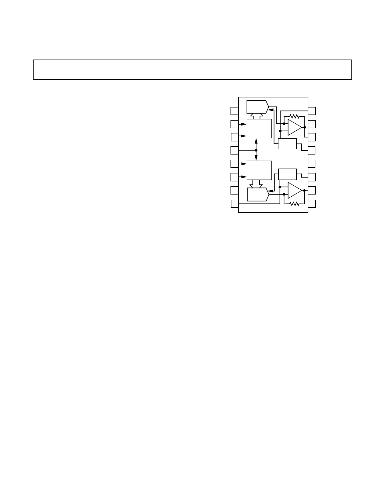
PRODUCT DESCRIPTION
The AD1868 is a complete dual 18-bit DAC offering excellent
performance while requiring a single +5 V power supply. It is
fabricated on Analog Devices’ ABCMOS wafer fabrication process. The monolithic chip includes CMOS logic elements, bipolar and MOS linear elements, and laser-trimmed thin-film
resistor elements. Careful design and layout techniques have resulted in low distortion, low noise, high channel separation, and
low power dissipation.
The DACs on the AD1868 chip employ a partially segmented
architecture. The first three MSBs of each DAC are segmented
into seven elements. The 15 LSBs are produced using standard
R-2R techniques. The segments and R-2R resistors are laser
trimmed to provide extremely low total harmonic distortion.
The AD1868 requires no deglitcher or trimming circuitry. Low
noise is achieved through the use of two noise-reduction capacitors.
Each DAC is equipped with a high performance output amplifier. These amplifiers achieve fast settling and high slew rate,
producing ± 1 V signals at load currents up to ±1 mA. The
buffered output signal range is 1.5 V to 3.5 V. Reference voltages of 2.5 V are provided, eliminating the need for “False
Ground” networks.
A versatile digital interface allows the AD1868 to be directly
connected to all digital filter chips. Fast CMOS logic elements
allow for an input clock rate of up to 13.5 MHz. This allows for
operation at 2×, 4×, 8×, or 16× the sampling frequency for each
channel. The digital input pins of the AD1868 are TTL and
+5 V CMOS compatible.
*Protected by U.S. Patent Numbers: 3,961,326; 4,141,004; 4,349,811;
4,857,862; and patents pending.
REV. A
Information furnished by Analog Devices is believed to be accurate and
reliable. However, no responsibility is assumed by Analog Devices for its
use, nor for any infringements of patents or other rights of third parties
which may result from its use. No license is granted by implication or
otherwise under any patent or patent rights of Analog Devices.
The AD1868 operates on +5 V power supplies. The digital supply, V
duced digital feedthrough. Separate analog and digital ground
pins are also provided. In systems employing a single +5 volt
power supply, V
tery operated systems, operation will continue even with reduced
supply voltage. Typically, the AD1868 dissipates 50 mW.
The AD1868 is packaged in either a 16-pin plastic DIP or a 16pin plastic SOIC package. Operation is guaranteed over the temperature range of –35°C to +85°C and over the voltage supply
range of 4.75 V to 5.25 V.
PRODUCT HIGHLIGHTS
1. Single-supply operation @ +5 V.
2. 50 mW power dissipation (typical).
3. THD+N is 0.004% (typical).
4. Signal-to-Noise Ratio is 97.5 dB (typical).
5. 108 dB channel separation (minimum).
6. Compatible with all digital filter chips.
7. 16-pin DIP and 16-pin SOIC packages.
8. No deglitcher required.
9. No external adjustments required.
One Technology Way, P.O. Box 9106, Norwood, MA 02062-9106, U.S.A.
Tel: 617/329-4700 Fax: 617/326-8703
FUNCTIONAL BLOCK DIAGRAM
, can be separated from the analog supply, VS, for re-
L
and VS should be connected together. In bat-
L
AD1868–SPECIFICA TIONS
WARNING!
ESD SENSITIVE DEVICE
(typical at TA = +258C and +5 V supplies unless otherwise noted)
Min Typ Max Units
RESOLUTION 18 Bit
DIGITAL INPUTS V
IH
V
IL
, VIH = V
I
IH
, VIL = DGND 1.0 µA
I
IL
L
2.4 V
0.8 V
1.0 µA
Maximum Clock Input Frequency 13.5 MHz
ACCURACY
Gain Error ±1 % of FSR
Gain Matching ±1 % of FSR
Midscale Error ±15 mV
Midscale Error Matching ±10 mV
Gain Linearity Error ±3dB
DRIFT (0°C to +70°C)
Gain Drift ±100 ppm/°C
Midscale Drift ±100 µV/°C
TOTAL HARMONIC DISTORTION + NOISE
0 dB, 990.5 Hz AD1868N 0.004 0.008 %
AD1868N-J 0.004 0.006 %
–20 dB, 990.5 Hz AD1868N 0.020 0.08 %
AD1868N-J 0.020 0.08 %
–60 dB, 990.5 Hz AD1868N 2.0 5.0 %
AD1868N-J 2.0 5.0 %
CHANNEL SEPARATION 1 kHz, 0 dB 108 NIL* dB
SIGNAL-TO-NOISE RATIO (with A-Weight Filter) 95 97.5 dB
D-RANGE (with A-Weight Filter) 86 92 dB
OUTPUT
Voltage Output Pins (V
L, VOR)
O
Output Range (±3%) ±1V
Output Impedance 0.1 Ω
Load Current ±1mA
Bias Voltage Pins (V
L, VBR)
B
Output Voltage +2.5 V
Output Impedance 350 Ω
POWER SUPPLY
Specification, V
Operation, V
and V
L
and V
L
S
S
4.75 5 5.25 V
3.5 5.25 V
+I, VL and VS = 5 V 10 14 mA
POWER DISSIPATION 50 70 mW
TEMPERATURE RANGE
Specification 0 25 70 °C
Operation –35 85 °C
Storage –60 100 °C
*Above 115 dB.
Specifications subject to change without notice.
ABSOLUTE MAXIMUM RATINGS*
VL to DGND . . . . . . . . . . . . . . . . . . . . . . . . . . . . . .0 V to 6 V
V
to AGND . . . . . . . . . . . . . . . . . . . . . . . . . . . . . .0 V to 6 V
S
AGND to DGND . . . . . . . . . . . . . . . . . . . . . . . . . . . . ±0.3 V
Digital Inputs to DGND . . . . . . . . . . . . . . . . . . . . .–0.3 to V
*Stresses greater than those listed under “Absolute Maximum Ratings” may cause
permanent damage to the device. This is a stress rating only and functional
operation of the device at these or any other conditions above those indicated in the
operational section of this specification is not implied. Exposure to absolute
maximum rating conditions for extended periods may affect device reliability.
L
Soldering . . . . . . . . . . . . . . . . . . . . . . . . . . . . .+300°C, 10 sec
CAUTION
ESD (electrostatic discharge) sensitive device. Electrostatic charges as high as 4000 V readily
accumulate on the human body and test equipment and can discharge without detection.
Although the AD1868 features proprietary ESD protection circuitry, permanent damage may
occur on devices subjected to high energy electrostatic discharges. Therefore, proper ESD
precautions are recommended to avoid performance degradation or loss of functionality.
–2–
REV. A
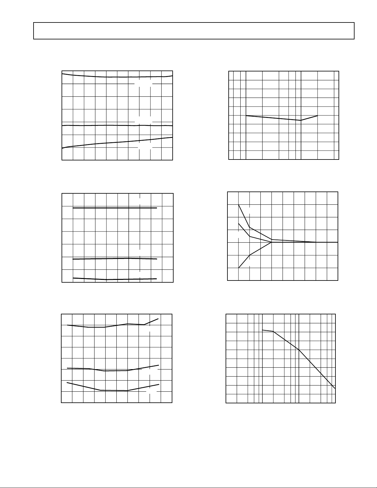
Typical Per formance of the AD1868
150
140
130
120
110
100
FREQUENCY – Hz
CHANNEL SEPARATION – dB
10
3
10
4
–30
AD1868
–40
–50
–60
–70
THD +N – dB
–80
–90
–100
0.5 2.5 4.5
6.5 8.5 10.5 12.5 14.5
FREQUENCY – kHz
–60dB
–20dB
0dB
16.5 18.5 20.5
Figure 1. THD+N vs. Frequency
–20
–30
–40
–50
–60
THD +N – dB
–70
–80
–90
4.4 4.6 4.8 5.0 5.2 5.4
VOLTAGE SUPPLY
–60dB
–20dB
0dB
Figure 2. Channel Separation vs. Frequency
8
6
0°C
4
2
25°C
0
–2
GAIN LINEARITY ERROR – dB
–4
–6
–100 –80 –60
70°C
INPUT AMPLITUDE – dB
–40
–20
–10
0
THD +N – dB
–100
REV. A
Figure 3. THD+N vs. Supply Voltage
–20
–
60dB
–40
–60
–
20dB
–80
0dB
–50 –30 –10 10 30 50 70 90 110 130
TEMPERATURE – °C
Figure 5. THD+N vs. Temperature
140
Figure 4. Gain Linearity Error vs. Input Amplitude
90
80
70
PSRR – dB
60
50
40
2
10
SUPPLY MODULATION FREQUENCY – Hz
3
10
4
10
Figure 6. Power Supply Rejection Ratio vs. Frequency
–3–
5
10
AD1868
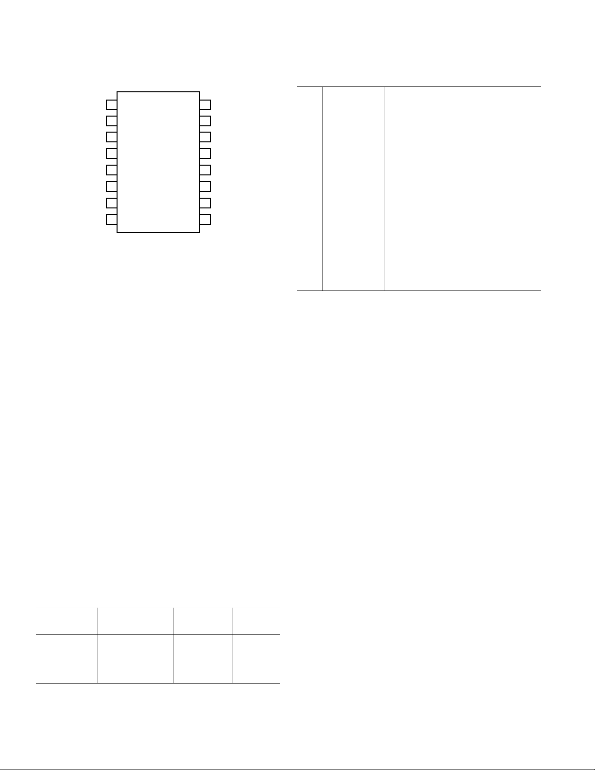
PIN CONFIGURATION
V
1
L
2
LL
3
DL
VBL
16
V
15
S
VOL
14
AD1868
CK
DR
LR
DGND
VBR
4
5
6
7
8
TOP VIEW
(Not To Scale)
13
NRL
AGND
12
11
NRR
VOR
10
V
S
9
DEFINITION OF SPECIFICATIONS
Total Harmonic Distortion + Noise
Total harmonic distortion plus noise (THD+N) is defined as
the ratio of the square root of the sum of the squares of the amplitudes of the harmonics and noise to the amplitude of the fundamental input frequency. It is usually expressed in percent (%)
or decibels (dB).
D-Range Distortion
D-range distortion is the ratio of the amplitude of the signal at
an amplitude of –60 dB to the amplitude of the distortion plus
noise. In this case, an A-weight filter is used. The value specified for D-range performance is the ratio measured plus 60 dB.
Signal-to-Noise Ratio
The signal-to-noise ratio is defined as the ratio of the amplitude
of the output when a full-scale output is present to the amplitude of the output with no signal present. It is expressed in
decibels (dB) and measured using an A-weight filter.
Gain Linearity
Gain linearity is a measure of the deviation of the actual output
amplitude from the ideal output amplitude. It is determined by
measuring the amplitude of the output signal as the amplitude
of that output signal is digitally reduced to a lower level. A perfect D/A converter exhibits no difference between the ideal and
actual amplitudes. Gain linearity is expressed in decibels (dB).
Midscale Error
Midscale error is the difference between the analog output and
the bias when the twos complement input code representing
midscale is loaded in the input register. Midscale error is expressed in mV.
PIN DESIGNATIONS
11V
L
Digital Supply (+5 Volts)
12 LL Left Channel Latch Enable
13 DL Left Channel Data Input
14 CK Clock Input
15 DR Right Channel Data Input
16 LR Right Channel Latch Enable
17 DGND Digital Common
18V
19V
10 V
R Right Channel Bias
B
S
R Right Channel Output
O
Analog Supply (+5 Volts)
11 NRR Right Channel Noise Reduction
12 AGND Analog Common
13 NRL Left Channel Noise Reduction
14 V
15 V
L Left Channel Output
O
S
Analog Supply (+5 Volts)
16 VBL Left Channel Bias
FUNCTIONAL DESCRIPTION
The AD1868 is a complete, voltage output dual 18-bit digital
audio DAC which operates with a single +5 volt supply. As
shown in the block diagram, each channel contains a voltage
reference, an 18-bit DAC, an output amplifier, an 18-bit input
latch, and an 18-bit serial-to-parallel input register.
The voltage reference section provides a reference voltage and a
false ground voltage for each channel. The low noise bandgap
circuits produce reference voltages that are unaffected by
changes in temperature, time, and power supply.
The output amplifier uses both MOS and bipolar devices and
incorporates an NPN class-A output stage. It is designed to produce high slew rate, low noise, low distortion, and optimal frequency response.
Each 18-bit DAC uses a combination of segmented decoder
and R-2R architecture to achieve good integral and differential
linearity. The resistors which form the ladder structure are fabricated with silicon-chromium thin film. Laser trimming of
these resistors further reduces linearity error, resulting in low
output distortion.
The input registers are fabricated with CMOS logic gates.
These gates allow fast switching speeds and low power consumption, contributing to the fast digital timing, low glitch, and
low power dissipation of the AD1868.
ORDERING GUIDE
THD + N Package
Model @ F
S
SNR Option*
AD1868N 0.008% 95 dB N-16
AD1868R 0.008% 95 dB R-16
AD1868N-J 0.006% 95 dB N-16
AD1868R-J 0.006% 95 dB R-16
*N = Plastic DIP; R = SOIC.
–4–
REV. A

AD1868
1
2
3
4
5
6
7
8
9
10
11
12
13
14
16
15
LL
DL
CK
DR
LR
DGND
NRL
AGND
NRR
V
L
VBR
V
B
L
V
S
VOL
V
O
R
AD1868
POWER
SUPPLY
0.1µF
0.1µF
4.7µF
4.7µF
V
S
V
LL
DL
CK
DR
LR
DGND
VBR
18-BIT
L
1
2
3
4
5
6
7
8
DAC
18-BIT
SERIAL
REGISTER
18-BIT
SERIAL
REGISTER
18-BIT
DAC
AD1868
–
+
V
REF
V
REF
+
–
L
V
16
B
V
15
S
VOL
14
NRL
13
AGND
12
NRR
11
V
R
10
O
V
9
S
Functional Block Diagram
ANALOG CIRCUIT CONSIDERATIONS
GROUNDING RECOMMENDATIONS
The AD1868 has two ground pins, designated as AGND (Pin
12) and DGND (Pin 7). The analog ground, AGND, serves as
the “high quality” reference ground for analog signals and as a
return path for the supply current from the analog portion of the
device. The system analog common should be located as close
as possible to Pin 12 to minimize any voltage drop which may
develop between these two points, although the internal circuit
is designed to minimize signal dependence of the analog return
current.
The digital ground, DGND, returns ground current from the
digital logic portion of the device. This pin should be connected
to the digital common node in the system. As shown in Figure
7, the analog and digital grounds should be joined at one point
in the system. When these two grounds are remotely connected
such as at the power supply ground, care should be taken to
minimize the voltage difference between the DGND and AGND
pins in order to ensure the specified performance.
POWER SUPPLIES AND DECOUPLING
The AD1868 has three power supply input pins. VS (Pins 9 and
15) provides the supply voltages which operate the analog portion of the device including the 18-bit DACs, the voltage references, and the output amplifiers. The V
supplies are designed
S
to operate with a +5 V supply. These pins should be decoupled
to analog common using a 0.1 µF capacitor. Good engineering
practice suggests that the bypass capacitors be placed as close as
possible to the package pins. This minimizes the inherent inductive effects of printed circuit board traces.
V
(Pin 1) operates the digital portions of the chip including the
L
input shift registers and the input latching circuitry. V
is also
L
designed to operate with a +5 V supply. This pin should be bypassed to digital common using a 0.1 µF capacitor, again placed
as close as possible to the package pin. Figure 7 illustrates the correct connection of the digital and analog supply bypass capacitors.
An important feature of the AD1868 audio DAC is its ability to
operate at reduced power supply voltages. This feature is very
important in portable battery operated systems. As the batteries
discharge, the supply voltage drops. Unlike any other audio
REV. A
DAC, the AD1868 can continue to function at supply voltages
as low as 3.5 V. Because of its unique design, the power requirements of the AD1868 diminish as the battery voltage drops, further extending the operating time of the system.
Figure 7. Recommended Circuit Schematic
NOISE REDUCTION CAPACITORS
The AD1868 has two noise reduction pins designated as NRL
(Pin 13) and NRR (Pin 11). It is recommended that external
noise reduction capacitors be connected from these pins to
AGND to reduce the output noise contributed by the voltage
reference circuitry. As shown in Figure 7, each of these pins
should be bypassed to AGND with a 4.7 µF or larger capacitor.
The connections between the capacitors, package pins and
AGND should be as short as possible to achieve the lowest
noise.
USING VBL AND VBR
The AD1868 has two bias voltage reference pins, designated as
V
R (Pin 8) and VBL (Pin 16). These pins supply a dc reference
B
voltage equal to the center of the output voltage swing. These
bias voltages replace “False Ground” networks previously required
in single-supply audio systems. At the same time, they allow dccoupled systems, improving audio performance.
Figure 8a illustrates the traditional approach used to generate
False Ground voltages in single-supply audio systems. This circuit requires additional power and circuit board space.
–V
DGND
+V
CLK
DATA
S
1
16-BIT
LATCH
2
3
4
5
6
7
8
REGISTER
CONTROL
LOGIC
AD1851
SERIAL
INPUT
NC = NO CONNECT
L
NC
LE
NC
16-BIT
DAC
I
OUT
+V
16
S
15
TRIM
MSB
14
ADJ
I
13
OUT
AGND
12
11
SJ
R
10
F
V
9
OUT
Figure 8a. Schematic Using False Ground
–5–

AD1868
+
5V
1
2
3
4
5
6
7
8
AD1868
V
L
LL
DL
CK
DR
LR
DGND
VBR
VBL
V
NRL
AGND
NRR
V
16
15
V
S
L
14
O
13
12
11
R
10
O
V
S
9
+
5V
VOL
V
R
O
Figure 8b. Circuitry Using Voltage Biases
The AD1868 eliminates the need for “False Ground” circuitry.
V
R and VBL generate the required bias voltages previously
B
generated by the “False Ground.” As shown in Figure 8b, V
and V
L may be used as the reference point in each output
B
R
B
channel. This permits a dc-coupled output signal path. This
eliminates ac-coupling capacitors and improves low frequency
performance. It should be noted that these bias outputs have
relatively high output impedance and will not drive output
currents larger than 100 µA without degrading the specified
performance.
DISTORTION PERFORMANCE AND TESTING
The THD+N figure of an audio DAC represents the amount of
undesirable signal produced during reconstruction and playback
of an audio waveform. Therefore, the THD+N specification
provides a direct method to classify and choose an audio DAC
for a desired level of performance.
Figure 1 illustrates the typical THD+N versus frequency performance of the AD1868. It is evident that the THD+N performance of the AD1868 remains stable at all three levels through
a wide range of frequencies. A load impedance of at least 2 kΩ is
recommended for best THD+N performance.
Analog Devices tests and grades all AD1868s on the basis of
THD+N performance. During the distortion test, a high speed
digital pattern generator transmits digital data to each channel
of the device under test. Eighteen-bit data is latched into the
DAC at 352.8 kHz (8× F
). The test waveform is a 990.5 Hz
S
sine wave with 0 dB, –20 dB, and –60 dB amplitudes. A 4096point FFT calculates total harmonic distortion + noise,
signal-to-noise ratio, and D-range. No deglitchers or external
adjustments are used.
DIGITAL CIRCUIT CONSIDERATIONS
INPUT DATA
The AD1868 digital input port employs five signals: Data Left
(DL), Data Right (DR), Latch Left (LL), Latch Right (LR) and
Clock (CLK). DL and DR are the serial inputs for the left and
right DACs, respectively. Input data bits are clocked into the input register on the rising edge of CLK. The falling edges of LL
and LR cause the last 18 bits which were clocked into the serial
registers to be shifted into the DACs, thereby updating the respective DAC outputs. For systems using only a single latch signal, LL and LR may be connected together. For systems using
only one DATA signal, DR and DL may be connected together.
Data is transmitted to the AD1868 in a bit stream composed of
18-bit words with a serial, twos complement, MSB first format.
Left and right channels share the Clock (CLK) signal.
Figure 9 illustrates the general signal requirements for data
transfer for the AD1868.
CLK
DR
DL
MSB
MSB
LL
LR
LSB
LSB
Figure 9. Control Signals
–6–
REV. A

AD1868
TIMING
Figure 10 illustrates the specific timing requirements that must
be met in order for the data transfer to be accomplished properly. The input pins of the AD1868 are TTL and 5 V CMOS
compatible.
The maximum clock rate of the AD1868 is specified to be at
least 13.5 MHz. This clock rate allows data transfer rates of 2×,
4×, 8×, and 16× F
(where FS equals 44.1 kHz). The applica-
S
tions section of this data sheet contains additional guidelines for
using the AD1868.
> 74./ ns
>30ns
>30ns
CLK
LATCH
ENABLE (LE)
DATA
>10ns
>30ns
MSB
1st BIT
>10ns
>60ns
INTERNAL DAC INPUT REGISTER
UPDATED WITH 18 MOST RECENT BITS
2nd BIT
LSB
(18th BIT)
>15ns
>40ns
BITS CLOCKED
TO SHIFT REGISTER
>40ns
NEXT
WORD
Figure 10. Input Signal Timing
APPLICATIONS OF THE AD1868
The AD1868 is a high performance audio DAC specifically designed for portable and automotive digital audio applications.
These market segments have technical requirements fundamentally different than those found in the high-end or home-use
market segments. Portable equipment must rely on components
which require low amounts of power to offer reasonable playing
times. Also, battery voltages drop as the end of the discharge
cycle is approached. The AD1868’s ability to operate from a
single +5 V supply makes it a good choice for battery-operated
gear. As the battery voltage drops, the power dissipation of the
+5V POWER
SUPPLY
AD1868 drops. This extends the usable battery life. Finally, as
the battery supply voltage drops, the bias voltages and signal
swings also drop, preventing signal clipping and abrupt degradation of distortion. Figure 3 illustrates that THD+N performance of the AD1868 remains constant through a wide range
of supply voltages.
Automotive equipment rely on components which are able to
consistently perform in a wide range of temperatures. In addition, due to the limited space available in automotive applications, small size is essential. The AD1868 is able to satisfy both
of these requirements. The device has guaranteed specified performance between 0°C and +70°C, and the 16-pin DIP or 16pin SOIC package is particularly attractive where overall size is
important.
Since the AD1868 provides dc bias voltages, the entire signal
chain can be dc-coupled. This eliminate ac-coupling capacitors
from the signal path, improving low frequency performance and
lowering system cost and size.
In summary, the AD1868 is an excellent choice for battery operated portable or automotive digital audio systems. In the following sections, some examples of high performance audio
applications featuring the AD1868 are described.
AD1868 with Sony CXD2550P Digital Filter
Figure 11 illustrates an 18-bit CD player design incorporating
an AD1868 DAC, a Sony CXD2550P digital filter and 2-pole
antialias filters. This high performance, single supply design operates at 8× F
and is suitable for portable and automotive ap-
S
plications. In this design, the CXD2550P filter transmits left
and right channel digital data to the AD1868. The left and
right latch signals, LL and LR, are both provided by the word
clock signal (LRCKO) of the digital filter. The digital data is
converted to low distortion output voltages by the output
amplifiers on the AD1868. Also, no deglitching circuitry or
external adjustments are required. Bypass capacitors, noise
reduction capacitors and the antialias filter details are omitted
for clarity.
REV. A
1
2
3
4
5
6
7
8
9
TEST
8Fs/4Fs
V
DD
INIT
CXD2550P
LRCK0
DATAL
DATAR
BCKO
SLOT
V
AD1868
16
L
18
17
16
15
14
SS
13
12
11
10
1
V
L
2
LL
3
DL
4
CK
5
DR
6
LR
7
DGND
8
VBR
V
V
NRL
AGND
NRR
VOR
B
V
15
S
L
14
O
13
12
11
10
9
V
S
1
2
3
4
AGND
8
V
S
7
6
5
LEFT
CHANNEL
OUTPUT
RIGHT
CHANNEL
OUTPUT
Figure 11. AD1868 with Sony CXD2550P Digital Filter
–7–

AD1868
ADDITIONAL APPLICATIONS
In addition to CD player designs, the AD1868 is suitable for
similar applications such as DAT, portable musical instruments, Laptop and Notebook personal computers, and PC audio I/O boards. The circuit techniques illustrated are directly
applicable in those applications.
+5V POWER
SUPPLY
SM5813
BCKO
WCKO
DOL
DOR
V
VSS2
OW18
OW20
COB
28
27
26
25
24
23
22
DD
21
20
19
18
17
16
15
1
2
3
4
5
6
7
8
1
V
SS
9
10
11
12
13
14
1
V
LL
2
3
DL
4
CK
5
DR
LR
6
7
DGND
8
V
Figures 12, 13, and 14 show connection diagrams for the
AD1868 with popular digital filter chips from NPC and
Yamaha. Each application operates at 8× F
operation. Please
S
refer to the appropriate sections of this data sheet for additional
information.
AD1868
16
L
V
V
NRL
AGND
NRR
V
O
B
V
15
S
14
L
O
13
12
11
10
R
V
9
S
LOW
PASS
FILTER
LOW
PASS
FILTER
LEFT
CHANNEL
OUTPUT
RIGHT
CHANNEL
OUTPUT
L
R
B
SM5818AP
1
2
3
4
5
6
7
VSS
8
Figure 12. AD1868 with NPC SM5813 Digital Filter
+5V POWER
SUPPLY
AD1868
V
BCKO
WDCO
DOR
DOL
DD
16
15
14
13
12
11
10
9
1
V
L
2
LL
3
DL
4
CK
5
DR
6
LR
7
DGND
VBR
8
V
VOL
NRL
AGND
NRR
V
O
L
16
B
15
V
S
14
13
12
11
R
10
9
V
S
LOW
PASS
FILTER
LOW
PASS
FILTER
Figure 13. AD1868 with NPC SM5818AP Digital Filter
LEFT
CHANNEL
OUTPUT
RIGHT
CHANNEL
OUTPUT
–8–
REV. A

+5V POWER
SUPPLY
AD1868
YM3434
16/18
ST
V
BCO
WCO
DRO
DLO
16
15
14
13
SS
12
11
10
9
1
2
3
4
5
6
7
8
1
2
3
4
VDD2
5
6
7
V
1
8
DD
V
L
LL
DL
CK
DR
LR
DGND
VBR
AD1868
V
VOL
NRL
AGND
NRR
V
L
16
B
V
15
S
14
13
12
11
10
R
O
V
9
S
LOW
PASS
FILTER
LOW
PASS
FILTER
LEFT
CHANNEL
OUTPUT
RIGHT
CHANNEL
OUTPUT
Figure 14. AD1868 with Yamaha YM3434 Digital Filter
OTHER DIGITAL AUDIO COMPONENTS AVAILABLE FROM ANALOG DEVICES
–V
S
1
16-BIT
LATCH
16-BIT
DAC
+V
16
S
–V
S
1
18-BIT
LATCH
18-BIT
DAC
+V
S
16
DGND
+V
NC
CLK
DATA
–V
2
3
L
4
5
LE
6
7
8
L
SERIAL
INPUT
REGISTER
CONTROL
LOGIC
I
OUT
15
TRIM
MSB
14
ADJ
I
13
AGND
12
11
SJ
R
10
V
9
AD1856
NC = NO CONNECT
AD1856 16-Bit Audio DAC
Complete, No External Components Required
16-Pin DIP or SOIC Package
Standard Pinout
Low Cost
OUT
F
OUT
DGND
+V
NC
CLK
LE
DATA
–V
2
3
L
4
5
6
7
8
L
SERIAL
INPUT
REGISTER
CONTROL
LOGIC
I
OUT
15
14
13
12
11
10
9
AD1860
NC = NO CONNECT
AD1860 18-Bit Audio DAC
Complete, No External Components Required
102 dB SNR Minimum
16-Pin DIP or SOIC Package
Standard Pinout
TRIM
MSB
ADJ
I
OUT
AGND
SJ
R
F
V
OUT
REV. A
–9–

AD1868
1
2
3
4
5
6
7
8
9
10
11
12
13
14
15
16
18-BIT
LATCH
18-BIT
DAC
SERIAL
INPUT
REGISTER
CONTROL
LOGIC
AD1861
DGND
NC
CLK
LE
DATA
NC = NO CONNECT
TRIM
MSB
ADJ
AGND
SJ
–V
S
+V
L
+V
S
I
OUT
V
OUT
R
F
I
OUT
NC
REFERENCE
AD1865
–V
S
AGND
R
F
TRIM
MSB
I
OUT
DGND
+V
S
1
2
3
4
5
6
7
8
9
10
11
12
24
23
22
21
20
19
18
17
16
15
14
13
TRIM
SJ
V
OUT
NC
DL
LL
MSB
I
OUT
AGND
R
F
SJ
V
OUT
+V
L
DR
LR
CK
REFERENCE
18-BIT
LATCH
18-BIT
DAC
18-BIT
DAC
18-BIT
LATCH
–
+
–
+
NC = NO CONNECT
–V
DGND
+V
NC
CLK
DATA
NC
S
1
2
L
3
4
5
LE
6
7
8
16-BIT
LATCH
SERIAL
INPUT
REGISTER
CONTROL
LOGIC
AD1851
NC = NO CONNECT
AD1851 16-Bit PCM Audio DAC
107 dB SNR Minimum
16 × F
Capability
S
±5 V Supply
16-BIT
DAC
I
OUT
+V
16
S
15
TRIM
MSB
14
ADJ
I
13
OUT
AGND
12
11
SJ
R
10
F
V
9
OUT
AD1861 18-Bit PCM Audio DAC
107 dB SNR Minimum
16 × F
Capability
S
±5 V Supply
–V
1
S
TRIM
2
MSB
I
OUT
AGND
SJ
R
F
V
OUT
+V
DR
CK
L
LR
10
11
12
REFERENCE
3
4
5
6
7
8
9
18-BIT
LATCH
AD1864 Dual 18-Bit Audio DAC
Complete, No External Components
THD+N = 0.004% (typical)
AD1864
REFERENCE
–
+
18-BIT
DAC
High Performance
Low Crosstalk
24-Pin DIP
18-BIT
DAC
–
+
18-BIT
LATCH
+V
24
S
TRIM
23
MSB
22
I
21
OUT
20
AGND
SJ
19
R
18
F
V
17
OUT
–V
16
L
15
DL
LL
14
DGND
13
AD1865 Dual 18-Bit Audio DAC
107 dB SNR Minimum
16 × F
Capability
S
THD+N = 0.004% (typical)
±5 V Supply
–10–
REV. A

AD1868
–V
–V
TRIM
+V
CLK
LE
DATA
–V
1
S
2
S
3
L
4
5
INPUT
6
DIGITAL
OFFSET
7
8
L
&
VOLTAGE
REFERENCE
20-BIT
DAC
AD1862
AD1862 20-Bit, Low Noise Audio DAC
110 dB SNR Minimum
THD+N = 0.0019% (typical)
±1 dB Gain Linearity
16-Pin Plastic DIP
+V
16
S
NR
15
2
ADJ
14
NR
13
1
12
AGND
I
11
OUT
R
10
F
DGND
9
REV. A
–11–

AD1868
OUTLINE DIMENSIONS
Dimensions shown in inches and (mm).
Plastic DIP (N) Package
16
18
0.87 (22.1) MAX
0.18
(4.57)
0.018 (0.46)
0.033 (0.84) 0.1 (2.54)
9
0.25
(6.35)
0.035
(0.89)
0.125
(3.18)
MIN
0.31
(7.87)
Plastic SOIC (R) Package
0.019 (0.49)
9
0.419
(10.65)
8
0.299
(7.60)
0.012
(0.3)
0.030
(0.75)
16
1
0.413 (10.50)
0.050
(1.27)
REF
0.011
(0.28)
0.3 (7.62)
0.104
(2.65)
0.18
(4.57)
MAX
C1478–7–10/90
0.013 (0.32)
–12–
0.042 (1.07)
PRINTED IN U.S.A.
REV. A
 Loading...