

REF OUT
SHA
COMP
20k
10k
5k
2.5k
2.5k
5k
12
12
AD1674
AGND
BIP OFF
REF IN
20V
IN
10V
IN
IDAC
12
CONTROL
CE
12/8
CS
R/C
A
0
5k
10k
SAR
CLOCK
A
10V
REF
REGISTERS / 3-STATE OUTPUT BUFFERS
DAC
STS
DB11 (MSB)
DB0 (LSB)
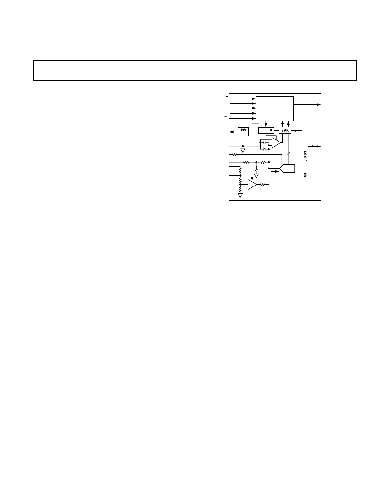
12-Bit 100 kSPS
a
FEATURES
Complete Monolithic 12-Bit 10 ms Sampling ADC
On-Board Sample-and-Hold Amplifier
Industry Standard Pinout
8- and 16-Bit Microprocessor Interface
AC and DC Specified and Tested
Unipolar and Bipolar Inputs
65 V, 610 V, 0 V–10 V, 0 V–20 V Input Ranges
Commercial, Industrial and Military Temperature
Range Grades
MIL-STD-883 and SMD Compliant Versions Available
PRODUCT DESCRIPTION
The AD1674 is a complete, multipurpose, 12-bit analog-todigital converter, consisting of a user-transparent onboard
sample-and-hold amplifier (SHA), 10 volt reference, clock and
three-state output buffers for microprocessor interface.
The AD1674 is pin compatible with the industry standard
AD574A and AD674A, but includes a sampling function while
delivering a faster conversion rate. The on-chip SHA has a wide
input bandwidth supporting 12-bit accuracy over the full
Nyquist bandwidth of the converter.
The AD1674 is fully specified for ac parameters (such as S/(N+D)
ratio, THD, and IMD) and dc parameters (offset, full-scale
error, etc.). With both ac and dc specifications, the AD1674 is
ideal for use in signal processing and traditional dc measurement applications.
The AD1674 design is implemented using Analog Devices’
BiMOS II process allowing high performance bipolar analog circuitry to be combined on the same die with digital CMOS logic.
Five different temperature grades are available. The AD1674J
and K grades are specified for operation over the 0°C to +70°C
temperature range. The A and B grades are specified from
–40°C to +85°C; the AD1674T grade is specified from –55°C
to +125°C. The J and K grades are available in both 28-lead
plastic DIP and SOIC. The A and B grade devices are available
in 28-lead hermetically sealed ceramic DIP and 28-lead SOIC.
The T grade is available in 28-lead hermetically sealed ceramic
DIP.
*Protected by U. S. Patent Nos. 4,962,325; 4,250,445; 4,808,908; RE30586.
A/D Converter
AD1674*
FUNCTIONAL BLOCK DIAGRAM
PRODUCT HIGHLIGHTS
1. Industry Standard Pinout: The AD1674 utilizes the pinout
established by the industry standard AD574A and AD674A.
2. Integrated SHA: The AD1674 has an integrated SHA which
supports the full Nyquist bandwidth of the converter. The
SHA function is transparent to the user; no wait-states are
needed for SHA acquisition.
3. DC and AC Specified: In addition to traditional dc specifications, the AD1674 is also fully specified for frequency domain ac parameters such as total harmonic distortion,
signal-to-noise ratio and input bandwidth. These parameters
can be tested and guaranteed as a result of the onboard
SHA.
4. Analog Operation: The precision, laser-trimmed scaling and
bipolar offset resistors provide four calibrated ranges:
0 V to +10 V and 0 V to +20 V unipolar, –5 V to +5 V and
–10 V to +10 V bipolar. The AD1674 operates on +5 V and
±12 V or ±15 V power supplies.
5. Flexible Digital Interface: On-chip multiple-mode
three-state output buffers and interface logic allow direct
connection to most microprocessors.
REV. C
Information furnished by Analog Devices is believed to be accurate and
reliable. However, no responsibility is assumed by Analog Devices for its
use, nor for any infringements of patents or other rights of third parties
which may result from its use. No license is granted by implication or
otherwise under any patent or patent rights of Analog Devices.
One Technology Way, P.O. Box 9106, Norwood, MA 02062-9106, U.S.A.
Tel: 617/329-4700 Fax: 617/326-8703
AD1674–SPECIFICA TIONS
(T
to T
, VCC = +15 V 6 10% or +12 V 6 5%, V
MAX
DC SPECIFICATIONS
MIN
–12 V 6 5% unless otherwise noted)
AD1674J AD1674K
Parameter Min Typ Max Min Typ Max Unit
RESOLUTION 12 12 Bits
INTEGRAL NONLINEARITY (INL) ±1 ±1/2 LSB
DIFFERENTIAL NONLINEARITY (DNL)
(No Missing Codes) 12 12 Bits
UNIPOLAR OFFSET1 @ +25°C ±3 ±2 LSB
BIPOLAR OFFSET1 @ +25°C ±6 ±4 LSB
FULL-SCALE ERROR
1, 2
@ +25°C
(with Fixed 50 Ω Resistor from REF OUT to REF IN) 0.1 0.25 0.1 0.25 % of FSR
TEMPERATURE RANGE 0 +70 0 +70 °C
TEMPERATURE DRIFT
Unipolar Offset
Bipolar Offset
Full-Scale Error
2
2
2
3
POWER SUPPLY REJECTION
VCC = 15 V ± 1.5 V or 12 V ± 0.6 V ±2 ±1 LSB
V
= 5 V ± 0.5 V ±1/2 ±1/2 LSB
LOGIC
VEE = –15 V ± 1.5 V or –12 V ± 0.6 V ±2 ±1 LSB
= +5 V 6 10%, VEE = –15 V 6 10% or
LOGIC
±2 ±1 LSB
±2 ±1 LSB
±6 ±3 LSB
ANALOG INPUT
Input Ranges
Bipolar –5 +5 –5 +5 Volts
–10 +10 –10 +10 Volts
Unipolar 0 +10 0 +10 Volts
0 +20 0 +20 Volts
Input Impedance
10 Volt Span 357357 kΩ
20 Volt Span 6 10 14 6 10 14 kΩ
POWER SUPPLIES
Operating Voltages
V
LOGIC
V
CC
V
EE
+4.5 +5.5 +4.5 +5.5 Volts
+11.4 +16.5 +11.4 +16.5 Volts
–16.5 –11.4 –16.5 –11.4 Volts
Operating Current
I
LOGIC
I
CC
I
EE
58 58 mA
10 14 10 14 mA
14 18 14 18 mA
POWER DISSIPATION 385 575 385 575 mW
INTERNAL REFERENCE VOLTAGE 9.9 10.0 10.1 9.9 10.0 10.1 Volts
Output Current (Available for External Loads)
4
2.0 2.0 mA
(External Load Should Not Change During Conversion
NOTES
1
Adjustable to zero.
2
Includes internal voltage reference error.
3
Maximum change from 25°C value to the value at T
4
Reference should be buffered for ±12 V operation.
All min and max specifications are guaranteed.
Specifications subject to change without notice.
MIN
or T
MAX
.
–2–
REV. C
AD1674
AD1674A AD1674B AD1674T
Parameter Min Typ Max Min Typ Max Min Typ Max Unit
RESOLUTION 12 12 12 Bits
INTEGRAL NONLINEARITY (INL) ±1 ±1/2 ±1/2 LSB
±1 ±1/2 ±1 LSB
DIFFERENTIAL NONLINEARITY (DNL)
(No Missing Codes) 12 12 12 Bits
UNIPOLAR OFFSET1 @ +25°C ±2 ±2 ±2 LSB
BIPOLAR OFFSET1 @ +25°C ±6 ±3 ±3 LSB
FULL-SCALE ERROR
(with Fixed 50 Ω Resistor from REF OUT to REF IN) 0.1 0.25 0.1 0.125 0.1 0.125 % of FSR
TEMPERATURE RANGE –40 +85 –40 +85 –55 +125 °C
TEMPERATURE DRIFT
Unipolar Offset
Bipolar Offset
Full-Scale Error
POWER SUPPLY REJECTION
VCC = 15 V ± 1.5 V or 12 V ± 0.6 V ±2 ±1 ±1 LSB
= 5 V ± 0.5 V ±1/2 ±1/2 ±1/2 LSB
V
LOGIC
VEE = –15 V ± 1.5 V or –12 V ± 0.6 V ±2 ±1 ±1 LSB
1, 2
@ +25°C
3
2
2
2
±2 ±1 ±1 LSB
±2 ±1 ±2 LSB
±8 ±5 ±7 LSB
ANALOG INPUT
Input Ranges
Bipolar –5 +5 –5 +5 –5 +5 Volts
–10 +10 –10 +10 –10 +10 Volts
Unipolar 0 +10 0 +10 0 +10 Volts
0 +20 0 +20 0 +20 Volts
Input Impedance
10 Volt Span 357357357 kΩ
20 Volt Span 6 10 14 6 10 14 6 10 14 kΩ
POWER SUPPLIES
Operating Voltages
V
LOGIC
V
CC
V
EE
+4.5 +5.5 +4.5 +5.5 +4.5 +5.5 Volts
+11.4 +16.5 +11.4 +16.5 +11.4 +16.5 Volts
–16.5 –11.4 –16.5 –11.4 –16.5 –11.4 Volts
Operating Current
I
LOGIC
I
CC
I
EE
58 58 58 mA
10 14 10 14 10 14 mA
14 18 14 18 14 18 mA
POWER DISSIPATION 385 575 385 575 385 575 mW
INTERNAL REFERENCE VOLTAGE 9.9 10.0 10.1 9.9 10.0 10.1 9.9 10.0 10.1 Volts
Output Current (Available for External Loads)
4
2.0 2.0 2.0 mA
(External Load Should Not Change During Conversion
REV. C
–3–

AD1674–SPECIFICATIONS
(T
to T
, with VCC = +15 V 6 10% or +12 V 6 5%, V
MAX
= 100 kSPS, fIN = 10 kHz, stand-alone mode unless otherwise noted)
SAMPLE
AC SPECIFICATIONS
MIN
–12 V 6 5%, f
AD1674J/A AD1674K/B/T
Parameter Min Typ Max Min Typ Max Units
Signal to Noise and Distortion (S/N+D) Ratio
Total Harmonic Distortion (THD)
4
2, 3
69 70 70 71 dB
–90 –82 –90 –82 dB
Peak Spurious or Peak Harmonic Component –92 –82 –92 –82 dB
Full Power Bandwidth 1 1 MHz
Full Linear Bandwidth 500 500 kHz
Intermodulation Distortion (IMD)
5
Second Order Products –90 –80 –90 –80 dB
Third Order Products –90 –80 –90 –80 dB
SHA (Specifications are Included in Overall Timing Specifications)
Aperture Delay 50 50 ns
Aperture Jitter 250 250 ps
Acquisition Time 1 1 µs
= +5 V 6 10%, VEE = –15 V 610% or
LOGIC
1
0.008 0.008 %
DIGITAL SPECIFICATIONS
(for all grades T
VEE = –15 V 6 10% or –12 V 6 5%)
MIN
to T
, with VCC = +15 V 6 10% or +12 V 6 5%, V
MAX
= +5 V 6 10%,
LOGIC
Parameter Test Conditions Min Max Units
LOGIC INPUTS
V
IH
V
IL
I
IH
I
IL
C
IN
High Level Input Voltage +2.0 V
+0.5 V V
LOGIC
Low Level Input Voltage –0.5 +0.8 V
High Level Input Current (VIN = 5 V) VIN = V
LOGIC
–10 +10 µA
Low Level Input Current (VIN = 0 V) VIN = 0 V –10 +10 µA
Input Capacitance 10 pF
LOGIC OUTPUTS
V
OH
V
OL
I
OZ
C
OZ
NOTES
1
fIN amplitude = –0.5 dB (9.44 V p-p) 10 V bipolar mode unless otherwise noted. All measurements referred to –0 dB (9.997 V p-p) input signal unless
otherwise noted.
2
Specified at worst case temperatures and supplies after one minute warm-up.
3
See Figures 12 and 13 for other input frequencies and amplitudes.
4
See Figure 11.
5
fa = 9.08 kHz, fb = 9.58 kHz with f
All min and max specifications are guaranteed.
Specifications subject to change without notice.
High Level Output Voltage IOH = 0.5 mA +2.4 V
Low Level Output Voltage IOL = 1.6 mA +0.4 V
High-Z Leakage Current VIN = 0 to V
LOGIC
–10 +10 µA
High-Z Output Capacitance 10 pF
= 100 kHz. See Definition of Specifications section and Figure 15.
SAMPLE
–4–
REV. C

AD1674
HIGH
IMPEDANCE
CE
STS
DB11 – DB0
A
0
CS
__
R/C
_
t
HSR
t
SSRtHRR
t
SAR
t
HAR
t
DD
t
HL
HIGH
IMP.
DATA
VALID
t
HD
t
HS
t
SSR
V
CP
D
OUT
C
OUT
I
OH
I
OL
SWITCHING SPECIFICATIONS
(for all grades T
V
= +5 V 610%, VEE = –15 V 6 10% or –12 V 6 5%; VIL = 0.4 V,
LOGIC
VIH = 2.4 V unless otherwise noted)
MIN
to T
CONVERTER START TIMING (Figure 1)
Parameter Symbol Min Typ Max Min Typ Max Units
Conversion Time
8-Bit Cycle t
12-Bit Cycle t
STS Delay from CE t
CE Pulse Width t
CS to CE Setup t
CS Low During CE High t
R/C to CE Setup t
R/C Low During CE High t
A0 to CE Setup t
A
Valid During CE High t
0
J, K, A, B, Grades T Grade
C
C
DSC
HEC
SSC
HSC
SRC
HRC
SAC
HAC
78 78µs
910 910µs
200 225 ns
50 50 ns
50 50 ns
50 50 ns
50 50 ns
50 50 ns
00ns
50 50 ns
READ TIMING—FULL CONTROL MODE (Figure 2)
J, K, A, B, Grades T Grade
Parameter Symbol Min Typ Max Min Typ Max Units
Access Time t
Data Valid After CE Low t
Output Float Delay t
CS to CE Setup t
R/C to CE Setup t
A
to CE Setup t
0
CS Valid After CE Low t
R/C High After CE Low t
A
Valid After CE Low t
0
NOTES
1
tDD is measured with the load circuit of Figure 3 and is defined as the time
required for an output to cross 0.4 V or 2.4 V.
2
0°C to T
3
At –40°C.
4
At –55°C.
5
tHL is defined as the time required for the data lines to change 0.5 V when
MAX
.
DD
HD
HL
SSR
SRR
SAR
HSR
HRR
HAR
1
5
75 150 75 150 ns
25
20
2
3
25
15
2
4
ns
ns
150 150 ns
50 50 ns
00ns
50 50 ns
00ns
00ns
50 50 ns
loaded with the circuit of Figure 3.
All min and max specifications are guaranteed.
Specifications subject to change without notice.
Test V
CP
C
OUT
Access Time High Z to Logic Low 5 V 100 pF
Float Time Logic High to High Z 0 V 10 pF
Access Time High Z to Logic High 0 V 100 pF
Float Time Logic Low to High Z 5 V 10 pF
with VCC = +15 V 6 10% or +12 V 6 5%,
MAX
CE
R/C
STS
DB11 – DB0
__
CS
_
t
A
SAC
0
t
SSC
t
SRCtHRC
t
HSC
t
Figure 1. Converter Start Timing
Figure 2. Read Timing
DSC
t
HEC
t
HAC
t
C
HIGH IMPEDANCE
REV. C
Figure 3. Load Circuit for Bus Timing Specifications
–5–

AD1674
DATA
VALID
HIGH-Z
HIGH-Z
STS
DB11 – DB0
R/C
_
t
HRH
t
DS
t
C
t
DDRtHDR
t
HL
TIMING—STAND-ALONE MODE (Figures 4a and 4b)
J, K, A, B Grades T Grade
Parameter Symbol Min Typ Max Min Typ Max Units
Data Access Time t
Low R/
C Pulse Width t
STS Delay from R/
Data Valid After R/
C t
C Low t
STS Delay After Data Valid t
High R/C Pulse Width t
NOTE
All min and max specifications are guaranteed.
Specifications subject to change without notice.
t
HRL
_
R/C
t
DS
STS
t
HDR
DB11 – DB0
DATA
VALID
Figure 4a. Stand-Alone Mode Timing Low Pulse for R/
DDR
HRL
DS
HDR
HS
HRH
t
C
HIGH-Z
50 50 ns
25 25 ns
0.6 0.8 1.2 0.6 0.8 1.2 µs
150 150 ns
t
HS
DATA VALID
C
ABSOLUTE MAXIMUM RATINGS*
VCC to Digital Common . . . . . . . . . . . . . . . . . . . 0 to + 16.5 V
V
to Digital Common . . . . . . . . . . . . . . . . . . . . . 0 to –16.5 V
EE
V
to Digital Common . . . . . . . . . . . . . . . . . . 0 V to +7 V
LOGIC
Analog Common to Digital Common . . . . . . . . . . . . . . . ±1 V
Digital Inputs to Digital Common . . . –0.5 V to V
Analog Inputs to Analog Common . . . . . . . . . . . . V
LOGIC
EE
+0.5 V
to V
CC
20 VIN to Analog Common . . . . . . . . . . . . . . . . . VEE to +24 V
REF OUT . . . . . . . . . . . . . . . . . Indefinite Short to Common
150 150 ns
200 225 ns
Figure 4b. Stand-Alone Mode Timing High Pulse for R/
. . . . . . . . . . . . . . . . . . . . . . . . . . . Momentary Short to V
C
CC
Junction Temperature . . . . . . . . . . . . . . . . . . . . . . . . . +175°C
Power Dissipation . . . . . . . . . . . . . . . . . . . . . . . . . . . .825 mW
Lead Temperature, Soldering (10 sec) . . . . . . . +300°C, 10 sec
Storage Temperature . . . . . . . . . . . . . . . . . . .–65°C to +150°C
*Stresses above those listed under “Absolute Maximum Ratings” may cause
permanent damage to the device. This is a stress rating only and functional
operation of the device at these or any other conditions above those indicated in the
operational section of this specification is not implied. Exposure to absolute
maximum rating conditions for extended periods may affect device reliability.
CAUTION
ESD (electrostatic discharge) sensitive device. Electrostatic charges as high as 4000 V readily
accumulate on the human body and test equipment and can discharge without detection. Although
WARNING!
the AD1674 features proprietary ESD protection circuitry, permanent damage may occur on
devices subjected to high energy electrostatic discharges. Therefore, proper ESD precautions are
recommended to avoid performance degradation or loss of functionality.
ESD SENSITIVE DEVICE
ORDERING GUIDE
INL S/(N+D) Package Package
MIN
to T
)(T
MAX
MIN
to T
) Description Option
MAX
Model
1
Temperature Range (T
AD1674JN 0°C to +70°C ±1 LSB 69 dB Plastic DIP N-28
AD1674KN 0°C to +70°C ± 1/2 LSB 70 dB Plastic DIP N-28
AD1674JR 0°C to +70°C ±1 LSB 69 dB Plastic SOIC R-28
AD1674KR 0°C to +70°C ±1/2 LSB 70 dB Plastic SOIC R-28
AD1674AR –40°C to +85°C ±1 LSB 69 dB Plastic SOIC R-28
AD1674BR –40°C to +85°C ±1/2 LSB 70 dB Plastic SOIC R-28
AD1674AD –40°C to +85°C ±1 LSB 69 dB Ceramic DIP D-28
AD1674BD –40°C to +85°C ±1/2 LSB 70 dB Ceramic DIP D-28
AD1674TD –55°C to +125°C ±1 LSB 70 dB Ceramic DIP D-28
NOTES
1
For details on grade and package offerings screened in accordance with MIL-STD-883, refer to the Analog Devices Military Products Databook or current
AD1674/883B data sheet. SMD is also available.
2
N = Plastic DIP; D = Hermetic Ceramic DIP; R = Plastic SOIC.
–6–
REV. C
2

AD1674
A
A
A
A
A
TOP VIEW
(Not to Scale)
AD1674
18
28
27
24
23
22
26
25
21
20
19
17
16
15
13
1
2
5
6
7
3
4
8
9
10
12
14
V
LOGIC
CE
V
CC
A
0
REF OUT
AGND
REF IN
V
EE
BIP OFF
10V
IN
20V
IN
CS
12/8
R/C
STS
DB11(MSB)
DB8
DB7
DB6
DB10
DB9
DB5
DB4
DB3
DB2
DB1
DB0(LSB)
DGND
11
PIN DESCRIPTION
Symbol Pin No. Type Name and Function
AGND 9 P Analog Ground (Common).
A
0
BIP OFF 12 AI Bipolar Offset. Connect through a 50 Ω resistor to REF OUT for bipolar operation or to Analog
CE 6 DI Chip Enable. Chip Enable is Active HIGH and is used to initiate a convert or read operation.
CS 3 DI Chip Select. Chip Select is Active LOW.
DB11–DB8 27–24 DO Data Bits 11 through 8. In the 12-bit format (see 12/
DB7–DB4 23–20 DO Data Bits 7 through 4. In the 12-bit format these pins provide the middle 4 bits of data. In the
DB3–DB0 19–16 DO Data Bits 3 through 0. In the 12-bit format these pins provide the lower 4 bits of data. In the
DGND 15 P Digital Ground (Common).
REF OUT 8 AO +10 V Reference Output.
R/
C 5 DI Read/Convert. In the full control mode R/C is Active HIGH for a read operation and Active LOW
REF IN 10 AI Reference Input is connected through a 50 Ω resistor to +10 V Reference for normal operation.
STS 28 DO Status is Active HIGH when a conversion is in progress and goes LOW when the conversion is
V
CC
V
EE
V
LOGIC
10 V
IN
20 V
IN
12/
8 2 DI The 12/8 pin determines whether the digital output data is to be organized as two 8-bit words
TYPE: AI = Analog Input
4 DI Byte Address/Short Cycle. If a conversion is started with A0 Active LOW, a full 12-bit conversion
cycle is initiated. If A
results. During Read (R/
(DB4–DB11), and A
is Active HIGH during a convert start, a shorter 8-bit conversion cycle
0
C = 1) with 12/8 LOW, A0 = LOW enables the 8 most significant bits
= HIGH enables DB3–DB0 and sets DB7–DB4 = 0.
0
Common for unipolar operation.
8 and A0 pins), these pins provide the up-
per 4 bits of data. In the 8-bit format, they provide the upper 4 bits when A
disabled when A
is HIGH.
0
8-bit format they provide the middle 4 bits when Ao is LOW and all zeroes when A
8-bit format these pins provide the lower 4 bits of data when A
when A
is LOW.
0
is HIGH, they are disabled
0
for a convert operation. In the stand-alone mode, the falling edge of R/
is LOW and are
0
is HIGH.
0
C initiates a conversion.
completed.
7 P +12 V/+15 V Analog Supply.
11 P –12 V/–15 V Analog Supply.
1 P +5 V Logic Supply.
13 AI 10 V Span Input, 0 V to +10 V unipolar mode or –5 V to +5 V bipolar mode. When using the
AD1674 in the 20 V Span 10 V
should not be connected.
IN
14 AI 20 V Span Input, 0 V to +20 V unipolar mode or –10 V to +10 V bipolar mode. When using
the AD1674 in the 10 V Span 20 V
should not be connected.
IN
(12/8 LOW) or a single 12-bit word (12/8 HIGH).
AO = Analog Output
DI = Digital Input
DO = Digital Output
P = Power
FUNCTIONAL BLOCK DIAGRAM
12/8
CS
A
CE
R/C
0
CONTROL
PIN CONFIGURATION
STS
REV. C
REF OUT
AGND
REF IN
BIP OFF
20V
10V
10V
REF
20k
IN
5k
IN
2.5k
2.5k
CLOCK
5k
10k
10k
5k
SHA
COMP
IDAC
SAR
12
DAC
AD1674
12
DB11 (MSB)
DB0 (LSB)
12
REGISTERS / 3-STATE OUTPUT BUFFERS
–7–

AD1674
DEFINITION OF SPECIFICATIONS
INTEGRAL NONLINEARITY (INL)
The ideal transfer function for an ADC is a straight line drawn
between “zero” and “full scale.” The point used as “zero”
occurs 1/2 LSB before the first code transition. “Full scale” is
defined as a level 1 1/2 LSB beyond the last code transition.
Integral nonlinearity is the worst-case deviation of a code from
the straight line. The deviation of each code is measured from
the middle of that code.
DIFFERENTIAL NONLINEARITY (DNL)
A specification which guarantees no missing codes requires that
every code combination appear in a monotonic increasing
sequence as the analog input level is increased. Thus every code
must have a finite width. The AD1674 guarantees no missing
codes to 12-bit resolution; all 4096 codes are present over the
entire operating range.
UNIPOLAR OFFSET
The first transition should occur at a level 1/2 LSB above analog common. Unipolar offset is defined as the deviation of the
actual transition from that point at 25°C. This offset can be
adjusted as shown in Figure 11.
BIPOLAR OFFSET
In the bipolar mode the major carry transition (0111 1111 1111
to 1000 0000 0000) should occur for an analog value 1/2 LSB
below analog common. The bipolar offset error specifies the
deviation of the actual transition from that point at 25°C. This
offset can be adjusted as shown in Figure 12.
FULL-SCALE ERROR
The last transition (from 1111 1111 1110 to 1111 1111 1111)
should occur for an analog value 1 1/2 LSB below the nominal
full scale (9.9963 volts for 10 volts full scale). The full-scale
error is the deviation of the actual level of the last transition
from the ideal level at 25°C. The full-scale error can be adjusted
to zero as shown in Figures 11 and 12.
TEMPERATURE DRIFT
The temperature drifts for full-scale error, unipolar offset and
bipolar offset specify the maximum change from the initial
(25°C) value to the value at T
POWER SUPPLY REJECTION
MIN
or T
MAX
.
The effect of power supply error on the performance of the
device will be a small change in full scale. The specifications
show the maximum full-scale change from the initial value with
the supplies at various limits.
FREQUENCY-DOMAIN TESTING
The AD1674 is tested dynamically using a sine wave input and
a 2048 point Fast Fourier Transform (FFT) to analyze the
resulting output. Coherent sampling is used, wherein the ADC
sampling frequency and the analog input frequency are related
to each other by a ratio of integers. This ensures that an integral
multiple of input cycles is captured, allowing direct FFT processing without windowing or digital filtering which could mask
some of the dynamic characteristics of the device. In addition,
the frequencies are chosen to he “relatively prime” (no common
factors) to maximize the number of different ADC codes that
are present in a sample sequence. The result, called Prime
Coherent Sampling, is a highly accurate and repeatable measure
of the actual frequency-domain response of the converter.
NYQUIST FREQUENCY
An implication of the Nyquist sampling theorem, the “Nyquist
Frequency” of a converter is that input frequency which is onehalf the sampling frequency of the converter.
SIGNAL-TO-NOISE AND DISTORTION (S/N+D) RATIO
S/(N+D) is the ratio of the rms value of the measured input signal to the rms sum of all other spectral components below the
Nyquist frequency, including harmonics but excluding dc. The
value for S/(N+D) is expressed in decibels.
TOTAL HARMONIC DISTORTION (THD)
THD is the ratio of the rms sum of the first six harmonic components to the rms value of a full-scale input signal and is expressed as a percentage or in decibels. For input signals or
harmonics that are above the Nyquist frequency, the aliased
component is used.
INTERMODULATION DISTORTION (IMD)
With inputs consisting of sine waves at two frequencies, fa and
fb, any device with nonlinearities will create distortion products,
of order (m+n), at sum and difference frequencies of mfa ± nfb,
where m, n = 0, 1, 2, 3. . . . Intermodulation terms are those for
which m or n is not equal to zero. For example, the second
order terms are (fa + fb) and (fa – fb) and the third order terms
are (2fa + fb), (2fa – fb), (fa + 2fb) and (fa – 2fb). The IMD
products are expressed as the decibel ratio of the rms sum of the
measured input signals to the rms sum of the distortion terms.
The two signals are of equal amplitude and the peak value of
their sums is –0.5 dB from full scale. The IMD products are
normalized to a 0 dB input signal.
FULL-POWER BANDWIDTH
The full-power bandwidth is that input frequency at which the
amplitude of the reconstructed fundamental is reduced by 3 dB
for a full-scale input.
FULL-LINEAR BANDWIDTH
The full-linear bandwidth is the input frequency at which the
slew rate limit of the sample-hold-amplifier (SHA) is reached.
At this point, the amplitude of the reconstructed fundamental
has degraded by less than –0.1 dB. Beyond this frequency, distortion of the sampled input signal increases significantly.
APERTURE DELAY
Aperture delay is a measure of the SHA’s performance and is
measured from the falling edge of Read/Convert (R/
C) to when
the input signal is held for conversion.
APERTURE JITTER
Aperture jitter is the variation in aperture delay for successive
samples and is manifested as noise on the input to the A/D.
–8–
REV. C

T ypical Dynamic Performance–AD1674
f
= 100kSPS
SAMPLE
FULL-SCALE = +10V
0
–20
–40
–60
–80
AMPLITUDE – dB
–100
–120
101
INPUT FREQUENCY – kHz
THD
HARMONIC
2NDHARMONIC
100
1000
RD
3
10000
Figure 5. Harmonic Distortion vs.
Input Frequency
0
–20
–40
–60
–80
AMPLITUDE – dB
–100
–120
–140
5
0
FREQUENCY – kHz
Figure 8. Nonaveraged 2048 Point FFT
at 100 kSPS, f
= 25.049 kHz
IN
80
70
60
50
40
S/(N+D) – dB
30
20
10
0
0dB INPUT
–20dB INPUT
–60dB INPUT
100
101
INPUT FREQUENCY – kHz
Figure 6. S/(N+D) vs. Input Frequency
and Amplitude
0
–10
–20
–30
–40
–50
–60
–70
–80
–90
AMPLITUDE – dB
–100
–110
–120
–130
50
4540353025201510
5
0
Figure 9. IMD Plot for fIN = 9.08 kHz (fa), 9.58 kHz (fb)
GENERAL CIRCUIT OPERATION
The AD1674 is a complete 12-bit, 10 µs sampling analog-to-
digital converter. A block diagram of the AD1674 is shown on
page 7.
When the control section is commanded to initiate a conversion
(as described later), it places the sample-and-hold amplifier
(SHA) in the hold mode, enables the clock, and resets the successive approximation register (SAR). Once a conversion cycle
has begun, it cannot be stopped or restarted and data is not
available from the output buffers. The SAR, timed by the internal clock, will sequence through the conversion cycle and return
an end-of-convert flag to the control section when the conversion has been completed. The control section will then disable
the clock, switch the SHA to sample mode, and delay the STS
LOW going edge to allow for acquisition to 12-bit accuracy.
The control section will allow data read functions by external
command anytime during the SHA acquisition interval.
During the conversion cycle, the internal 12-bit, 1 mA full-scale
current output DAC is sequenced by the SAR from the most
significant bit (MSB) to the least significant bit (LSB) to provide an output that accurately balances the current through the
5 kΩ resistor from the input signal voltage held by the SHA.
The SHA’s input scaling resistors divide the input voltage by 2
for the 10 V input span and by 4 V for the 20 V input span,
maintaining a 1 mA full-scale output current through the 5 kΩ
resistor for both ranges. The comparator determines whether
the addition of each successively weighted bit current causes the
10000
1000
Figure 7. S/(N+D) vs. Input Amplitude
50
20 25 40
FREQUENCY – kHz
4535301510
DAC current sum to be greater than or less than the input current. If the sum is less, the bit is left on; if more, the bit is
turned off. After testing all the bits, the SAR contains a 12-bit
binary code which accurately represents the input signal to
within ±1/2 LSB.
CONTROL LOGIC
The AD1674 may be operated in one of two modes, the fullcontrol mode and the stand-alone mode. The full-control mode
utilizes all the AD1674 control signals and is useful in systems
that address decode multiple devices on a single data bus. The
stand-alone mode is useful in systems with dedicated input ports
available and thus not requiring full bus interface capability.
Table I is a truth table for the AD1674, and Figure 10 illustrates the internal logic circuitry.
Table I. AD1674A Truth Table
CE CS R/C 12/8 A0Operation
0 X X X X None
X 1 X X X None
1 0 0 X 0 Initiate 12-Bit Conversion
1 0 0 X 1 Initiate 8-Bit Conversion
1 0 1 1 X Enable 12-Bit Parallel Output
1 0 1 0 0 Enable 8 Most Significant Bits
1 0 1 0 1 Enable 4 LSBs +4 Trailing Zeroes
REV. C
–9–

AD1674
D
READ
EN
Q
QB
–10–
Q
D
EN
R
Q
S
CE
CS
R/C
A
0
12/8
Figure 10. Equivalent Internal Logic Circuitry
FULL-CONTROL MODE
Chip Enable (CE), Chip Select (
CS) and Read/ Convert (R/C)
are used to control Convert or Read modes of operation. Either
CE or
CS may be used to initiate a conversion. The state of R/C
when CE and
Read (R/
should be LOW before both CE and
CS are both asserted determines whether a data
C = 1) or a Convert (R/C = 0) is in progress. R/C
CS are asserted; if R/C is
HIGH, a Read operation will momentarily occur, possibly
resulting in system bus contention.
STAND-ALONE MODE
The AD1674 can be used in a “stand-alone” mode, which is
useful in systems with dedicated input ports available and thus
not requiring full bus interface capability. Stand-alone mode
applications are generally able to issue conversion start commands more precisely than full-control mode. This improves ac
performance by reducing the amount of control-induced aperture jitter.
In stand-alone mode, the control interface for the AD1674 and
AD674A are identical. CE and 12/
A
are wired LOW, and conversion is controlled by R/C. The
0
three-state buffers are enabled when R/
version starts when R/
C goes LOW. This gives rise to two pos-
8 are wired HIGH, CS and
C is HIGH and a con-
sible control signals—a high pulse or a low pulse. Operation
with a low pulse is shown in Figure 4a. In this case, the outputs
are forced into the high impedance state in response to the falling edge of R/
C and return to valid logic levels after the conversion cycle is completed. The STS line goes HIGH 200 ns after
R/
C goes LOW and returns low 1 µs after data is valid.
If conversion is initiated by a high pulse as shown in Figure 4b,
the data lines are enabled during the time when R/
The falling edge of R/
C starts the next conversion and the data
C is HIGH.
lines return to three-state (and remain three-state) until the next
high pulse of R/
C.
CONVERSION TIMING
Once a conversion is started, the STS line goes HIGH. Convert
start commands will be ignored until the conversion cycle is
complete. The output data buffers will be enabled a minimum
of 0.6 µs prior to STS going LOW. The STS line will return
LOW at the end of the conversion cycle.
VALUE OF A0 AT LAST
CONVERT COMMAND
EOC 12
EOC 8
S
R
The register control inputs, A
length and data format. If a conversion is started with A
a full 12-bit conversion cycle is initiated. If A
SAR RESET
Q
QB
NYBBLE A
NYBBLE B
NYBBLE C
NYBBLE B = 0
1µs DELAY-HOLD SETTLING
1µs DELAY-ACQUISITION
TO OUTPUT
BUFFERS
and 12/8, control conversion
0
CLK ENABLE
STATUS
HOLD/SAMPLE
is HIGH during a
0
LOW,
0
convert start, a shorter 8-bit conversion cycle results.
During data read operations, A
state buffers containing the 8 MSBs of the conversion result (A
determines whether the three-
0
0
= 0) or the 4 LSBs (A0 = 1) are enabled. The 12/8 pin determines whether the output data is to be organized as two 8-bit
words (12/
HIGH). In the 8-bit mode, the byte addressed when A
8 tied LOW) or a single 12-bit word (12/8 tied
is high
0
contains the 4 LSBs from the conversion followed by four trailing zeroes. This organization allows the data lines to be overlapped for direct interface to 8-bit buses without the need for
external three-state buffers.
INPUT CONNECTIONS AND CALIBRATION
The 10 V p-p and 20 V p-p full-scale input ranges of the
AD1674 accept the majority of signal voltages without the need
for external voltage divider networks which could deteriorate the
accuracy of the ADC.
The AD1674 is factory trimmed to minimize offset, linearity,
and full-scale errors. In many applications, no calibration trimming will be required and the AD1674 will exhibit the accuracy
limits listed in the specification tables.
In some applications, offset and full-scale errors need to be
trimmed out completely. The following sections describe the
correct procedure for these various situations.
UNIPOLAR RANGE INPUTS
Figure 11 illustrates the external connections for the AD1674 in
unipolar-input mode. The first output-code transition (from
0000 0000 0000 to 0000 0000 0001) should nominally occur
for an input level of +1/2 LSB (1.22 mV above ground for a 10 V
range; 2.44 mV for a 20 V range). To trim unipolar offset to this
nominal value, apply a +1/2 LSB signal between Pin 13 and
ground (10 V range) or Pin 14 and ground (20 V range) and adjust R1 until the first transition is located. If the offset trim is
not required, Pin 12 can be connected directly to Pin 9; the two
resistors and trimmer for Pin 12 are then not needed.
REV. C

AD1674
–15V
100k
100Ω
0 TO +10V
ANALOG
INPUTS
0 TO +20V
R1
100k
+15V
R2
100Ω
2 12/8
3 CS
4 A
0
5 R/C
6 CE
10 REF IN
8 REF OUT
12 BIP OFF
13 10V
14 20V
9 ANA COM
AD1674
IN
IN
STS 28
HIGH BITS
24-27
MIDDLE BITS
20-23
LOW BITS
16-19
+5V 1
+15V 7
–15V 11
DIG COM 15
Figure 11. Unipolar Input Connections with Gain and
Offset Trims
The full-scale trim is done by applying a signal 1 1/2 LSB below
the nominal full scale (9.9963 V for a 10 V range) and adjusting
R2 until the last transition is located (1111 1111 1110 to 1111
1111 1111). If full-scale adjustment is not required, R2 should
be replaced with a fixed 50 Ω ±1% metal film resistor. If REF
OUT is connected directly to REF IN, the additional full-scale
error will be approximately 1%.
BIPOLAR RANGE INPUTS
The connections for the bipolar-input mode are shown in Figure
12. Either or both of the trimming potentiometers can be
replaced with 50 Ω ± 1% fixed resistors if the specified AD1674
accuracy limits are sufficient for the application. If the pins are
shorted together, the additional offset and gain errors will be
approximately 1%.
To trim bipolar offset to its nominal value, apply a signal 1/2
LSB below midrange (–1.22 mV for a ± 5 V range) and adjust
R1 until the major carry transition is located (0111 1111 1111
to 1000 0000 0000). To trim the full-scale error, apply a signal
1 1/2 LSB below full scale (+4.9963 V for a ± 5 V range) and
adjust R2 to give the last positive transition (1111 1111 1110 to
1111 1111 1111). These trims are interactive so several iterations may be necessary for convergence.
A single-pass calibration can be done by substituting a negative
full-scale trim for the bipolar offset trim (error at midscale),
using the same circuit. First, apply a signal 1/2 LSB above minus
full scale (–4.9988 V for a ±5 V range) and adjust R1 until the
minus full-scale transition is located (0000 0000 0001 to 0000
0000 0000). Then perform the gain error trim as outlined above.
ANALOG
INPUTS
±5V
±10V
R2
100Ω
100Ω
R1
2 12/8
3 CS
4 A
0
5 R/C
6 CE
10 REF IN
8 REF OUT
12 BIP OFF
13 10V
14 20V
9 ANA COM
AD1674
IN
IN
STS 28
HIGH BITS
24-27
MIDDLE BITS
20-23
LOW BITS
16-19
+5V 1
+15V 7
–15V 11
DIG COM 15
Figure 12. Bipolar Input Connections with Gain and Offset
Trims
REFERENCE DECOUPLING
It is recommended that a 10 µF tantalum capacitor be con-
nected between REF IN (Pin 10) and ground. This has the
effect of improving the S/(N+D) ratio through filtering possible
broad-band noise contributions from the voltage reference.
BOARD LAYOUT
Designing with high resolution data converters requires careful
attention to board layout. Trace impedance is a significant issue.
At the 12-bit level, a 5 mA current through a 0.5 Ω trace will
develop a voltage drop of 2.5 mV, which is 1 LSB for a 10 V
full-scale range. In addition to ground drops, inductive and capacitive coupling need to be considered, especially when high
accuracy analog signals share the same board with digital signals. Finally, power supplies should be decoupled in order to
filter out ac noise.
The AD1674 has a wide bandwidth sampling front end. This
means that the AD1674 will “see” high frequency noise at the
input, which nonsampling (or limited-bandwidth sampling)
ADCs would ignore. Therefore, it’s important to make an effort
to eliminate such high frequency noise through decoupling or by
using an anti-aliasing filter at the analog input of the AD1674.
Analog and digital signals should not share a common path.
Each signal should have an appropriate analog or digital return
routed close to it. Using this approach, signal loops enclose a
small area, minimizing the inductive coupling of noise. Wide PC
tracks, large gauge wire, and ground planes are highly recommended to provide low impedance signal paths. Separate analog
and digital ground planes are also desirable, with a single interconnection point to minimize ground loops. Analog signals
should be routed as far as possible from digital signals and
should cross them (if necessary) only at right angles.
The AD1674 incorporates several features to help the user’s layout. Analog pins are adjacent to help isolate analog from digital
signals. Ground currents have been minimized by careful circuit
architecture. Current through AGND is 2.2 mA, with little
code-dependent variation. The current through DGND is dominated by the return current for DB11–DB0.
SUPPLY DECOUPLING
The AD1674 power supplies should be well filtered, well regulated, and free from high frequency noise. Switching power supplies are not recommended due to their tendency to generate
spikes which can induce noise in the analog system.
Decoupling capacitors should be used in very close layout proximity between all power supply pins and ground. A 10 µF tanta-
lum capacitor in parallel with a 0.1 µF disc ceramic capacitor
provides adequate decoupling over a wide range of frequencies.
An effort should be made to minimize the trace length between
the capacitor leads and the respective converter power supply
and common pins. The circuit layout should attempt to locate
the AD1674, associated analog input circuitry, and interconnections as far as possible from logic circuitry. A solid analog
ground plane around the AD1674 will isolate large switching
ground currents. For these reasons, the use of wire-wrap circuit
construction is not recommended; careful printed-circuit construction is preferred.
REV. C
–11–

AD1674
0.050 ±0.010
(1.27 ±0.254)
SEATING
PLANE
1.42 (36.07)
1.40 (35.56)
0.047 ±0.007
(1.19 ±0.178)
0.1 (2.54)
0.017 ±0.003
(0.43 ±0.076)
0.145 ±0.02
(3.68 ±0.51)
0.125
(3.17)
MIN
0.6 (15.24)
0.010 ±0.002
(0.254 ±0.05)
0.095
(2.41)
0.085
(2.16)
0.59 ±0.01
(14.98 ±0.254)
14
15
PIN 1
1
28
0.505 (12.83)
PIN 1
0.2992 (7.60)
0.2914 (7.40)
0.4193 (10.65)
0.3937 (10.00)
1
28
15
14
0.0125 (0.32)
0.0091 (0.23)
0.0500 (1.27)
0.0157 (0.40)
8°
0°
0.0291 (0.74)
0.0098 (0.25)
x 45°
0.0192 (0.49)
0.0138 (0.35)
0.0500 (1.27)
BSC
0.1043 (2.65)
0.0926 (2.35)
0.7125 (18.10)
0.6969 (17.70)
0.0118 (0.30)
0.0040 (0.10)
GROUNDING
If a single AD1674 is used with separate analog and digital
ground planes, connect the analog ground plane to AGND and
the digital ground plane to DGND keeping lead lengths as short
as possible. Then connect AGND and DGND together at the
AD1674. If multiple AD1674s are used or the AD1674 shares
analog supplies with other components, connect the analog and
digital returns together once at the power supplies rather than at
each chip. This prevents large ground loops which inductively
couple noise and allow digital currents to flow through the analog system.
GENERAL MICROPROCESSOR INTERFACE CONSIDERATIONS
A typical A/D converter interface routine involves several operations. First, a write to the ADC address initiates a conversion.
The processor must then wait for the conversion cycle to complete, since most ADCs take longer than one instruction cycle to
complete a conversion. Valid data can, of course, only be read
after the conversion is complete. The AD1674 provides an output signal (STS) which indicates when a conversion is in
progress. This signal can be polled by the processor by reading
it through an external three-state buffer (or other input port).
The STS signal can also be used to generate an interrupt upon
completion of a conversion, if the system timing requirements
are critical (bear in mind that the maximum conversion time of
the AD1674 is only 10 microseconds) and the processor has
other tasks to perform during the ADC conversion cycle. Another possible time-out method is to assume that the ADC will
take 10 microseconds to convert, and insert a sufficient number
of “no-op” instructions to ensure that 10 microseconds of processor time is consumed.
Once it is established that the conversion is finished, the data
can be read. In the case of an ADC of 8-bit resolution (or less),
a single data read operation is sufficient. In the case of converters with more data bits than are available on the bus, a choice of
data formats is required, and multiple read operations are
needed. The AD1674 includes internal logic to permit direct interface to 8-bit or 16-bit data buses, selected by the 12/
In 16-bit bus applications (12/
8 HIGH) the data lines (DB11
8 input.
through DB0) may be connected to either the 12 most significant or 12 least significant hits of the data bus. The remaining
four bits should be masked in software. The interface to an 8-bit
data bus (12/
DB4). The odd address (A
8 LOW) contains the 8 MSBs (DB11 through
HIGH) contains the 4 LSBs (DB3
0
through DB0) in the upper half of the byte, followed by four
trailing zeroes, thus eliminating bit masking instructions.
PIN 1
0.200
(5.080)
MAX
0.175 (4.45)
0.120 (3.05)
PACKAGE INFORMATION
Dimensions shown in inches and (mm).
28-Pin Ceramic DIP Package (D-28)
28-Lead Plastic DIP Package (N-28)
28
1
0.020 (0.508)
0.015 (0.381)
1.450 (38.83)
1.440 (35.576)
0.105 (2.67)
0.095 (2.41)
15
14
0.065 (1.65)
0.045 (1.14)
0.550 (13.97)
0.530 (13.462)
0.160 (4.06)
0.140 (3.56)
SEATING
PLANE
0.606 (15.39)
0.594 (15.09)
15
°
0
°
28-Lead Wide-Body SO Package (R-28)
0.012 (0.305)
0.008 (0.203)
C1425b–10–3/94
AD1674 Data Format for 8-Bit Bus
–12–
PRINTED IN U.S.A.
REV. C
 Loading...