REF OUT
SHA
COMP
20k
10k
5k
2.5k
2.5k
5k
12
12
AD1674
AGND
BIP OFF
REF IN
20V
IN
10V
IN
IDAC
12
CONTROL
CE
12/8
CS
R/C
A
0
5k
10k
SAR
CLOCK
A
10V
REF
REGISTERS / 3-STATE OUTPUT BUFFERS
DAC
STS
DB11 (MSB)
DB0 (LSB)
12-Bit 100 kSPS
a
FEATURES
Complete Monolithic 12-Bit 10 ms Sampling ADC
On-Board Sample-and-Hold Amplifier
Industry Standard Pinout
8- and 16-Bit Microprocessor Interface
AC and DC Specified and Tested
Unipolar and Bipolar Inputs
65 V, 610 V, 0 V–10 V, 0 V–20 V Input Ranges
Commercial, Industrial and Military Temperature
Range Grades
MIL-STD-883 and SMD Compliant Versions Available
PRODUCT DESCRIPTION
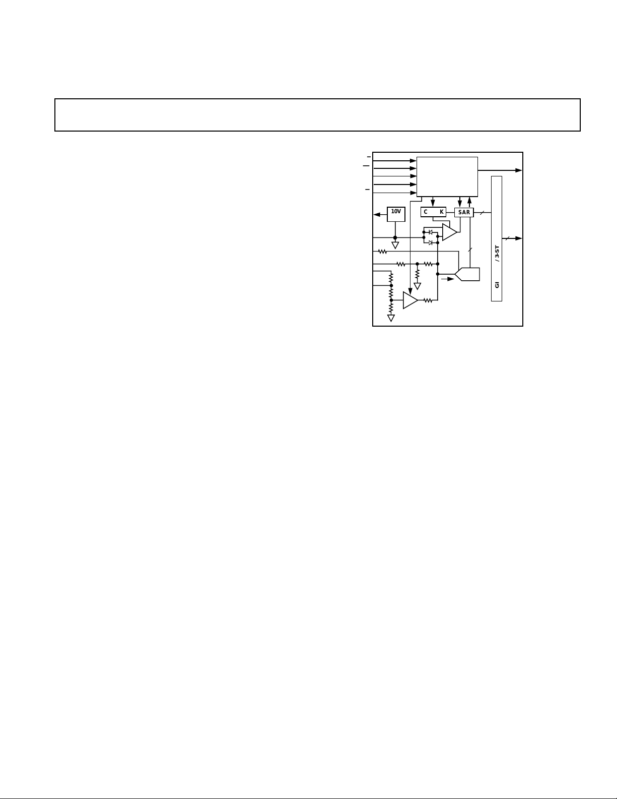
The AD1674 is a complete, multipurpose, 12-bit analog-todigital converter, consisting of a user-transparent onboard
sample-and-hold amplifier (SHA), 10 volt reference, clock and
three-state output buffers for microprocessor interface.
The AD1674 is pin compatible with the industry standard
AD574A and AD674A, but includes a sampling function while
delivering a faster conversion rate. The on-chip SHA has a wide
input bandwidth supporting 12-bit accuracy over the full
Nyquist bandwidth of the converter.
The AD1674 is fully specified for ac parameters (such as S/(N+D)
ratio, THD, and IMD) and dc parameters (offset, full-scale
error, etc.). With both ac and dc specifications, the AD1674 is
ideal for use in signal processing and traditional dc measurement applications.
The AD1674 design is implemented using Analog Devices’
BiMOS II process allowing high performance bipolar analog circuitry to be combined on the same die with digital CMOS logic.
Five different temperature grades are available. The AD1674J
and K grades are specified for operation over the 0°C to +70°C
temperature range. The A and B grades are specified from
–40°C to +85°C; the AD1674T grade is specified from –55°C
to +125°C. The J and K grades are available in both 28-lead
plastic DIP and SOIC. The A and B grade devices are available
in 28-lead hermetically sealed ceramic DIP and 28-lead SOIC.
The T grade is available in 28-lead hermetically sealed ceramic
DIP.
*Protected by U. S. Patent Nos. 4,962,325; 4,250,445; 4,808,908; RE30586.
A/D Converter
AD1674*
FUNCTIONAL BLOCK DIAGRAM
PRODUCT HIGHLIGHTS
1. Industry Standard Pinout: The AD1674 utilizes the pinout
established by the industry standard AD574A and AD674A.
2. Integrated SHA: The AD1674 has an integrated SHA which
supports the full Nyquist bandwidth of the converter. The
SHA function is transparent to the user; no wait-states are
needed for SHA acquisition.
3. DC and AC Specified: In addition to traditional dc specifications, the AD1674 is also fully specified for frequency domain ac parameters such as total harmonic distortion,
signal-to-noise ratio and input bandwidth. These parameters
can be tested and guaranteed as a result of the onboard
SHA.
4. Analog Operation: The precision, laser-trimmed scaling and
bipolar offset resistors provide four calibrated ranges:
0 V to +10 V and 0 V to +20 V unipolar, –5 V to +5 V and
–10 V to +10 V bipolar. The AD1674 operates on +5 V and
±12 V or ±15 V power supplies.
5. Flexible Digital Interface: On-chip multiple-mode
three-state output buffers and interface logic allow direct
connection to most microprocessors.
REV. C
Information furnished by Analog Devices is believed to be accurate and
reliable. However, no responsibility is assumed by Analog Devices for its
use, nor for any infringements of patents or other rights of third parties
which may result from its use. No license is granted by implication or
otherwise under any patent or patent rights of Analog Devices.
One Technology Way, P.O. Box 9106, Norwood, MA 02062-9106, U.S.A.
Tel: 617/329-4700 Fax: 617/326-8703

AD1674–SPECIFICA TIONS
(T
to T
, VCC = +15 V 6 10% or +12 V 6 5%, V
MAX
DC SPECIFICATIONS
MIN
–12 V 6 5% unless otherwise noted)
AD1674J AD1674K
Parameter Min Typ Max Min Typ Max Unit
RESOLUTION 12 12 Bits
INTEGRAL NONLINEARITY (INL) ±1 ±1/2 LSB
DIFFERENTIAL NONLINEARITY (DNL)
(No Missing Codes) 12 12 Bits
UNIPOLAR OFFSET1 @ +25°C ±3 ±2 LSB
BIPOLAR OFFSET1 @ +25°C ±6 ±4 LSB
FULL-SCALE ERROR
1, 2
@ +25°C
(with Fixed 50 Ω Resistor from REF OUT to REF IN) 0.1 0.25 0.1 0.25 % of FSR
TEMPERATURE RANGE 0 +70 0 +70 °C
TEMPERATURE DRIFT
Unipolar Offset
Bipolar Offset
Full-Scale Error
2
2
2
3
POWER SUPPLY REJECTION
VCC = 15 V ± 1.5 V or 12 V ± 0.6 V ±2 ±1 LSB
V
= 5 V ± 0.5 V ±1/2 ±1/2 LSB
LOGIC
VEE = –15 V ± 1.5 V or –12 V ± 0.6 V ±2 ±1 LSB
= +5 V 6 10%, VEE = –15 V 6 10% or
LOGIC
±2 ±1 LSB
±2 ±1 LSB
±6 ±3 LSB
ANALOG INPUT
Input Ranges
Bipolar –5 +5 –5 +5 Volts
–10 +10 –10 +10 Volts
Unipolar 0 +10 0 +10 Volts
0 +20 0 +20 Volts
Input Impedance
10 Volt Span 357357 kΩ
20 Volt Span 6 10 14 6 10 14 kΩ
POWER SUPPLIES
Operating Voltages
V
LOGIC
V
CC
V
EE
+4.5 +5.5 +4.5 +5.5 Volts
+11.4 +16.5 +11.4 +16.5 Volts
–16.5 –11.4 –16.5 –11.4 Volts
Operating Current
I
LOGIC
I
CC
I
EE
58 58 mA
10 14 10 14 mA
14 18 14 18 mA
POWER DISSIPATION 385 575 385 575 mW
INTERNAL REFERENCE VOLTAGE 9.9 10.0 10.1 9.9 10.0 10.1 Volts
Output Current (Available for External Loads)
4
2.0 2.0 mA
(External Load Should Not Change During Conversion
NOTES
1
Adjustable to zero.
2
Includes internal voltage reference error.
3
Maximum change from 25°C value to the value at T
4
Reference should be buffered for ±12 V operation.
All min and max specifications are guaranteed.
Specifications subject to change without notice.
MIN
or T
MAX
.
–2–
REV. C

AD1674
AD1674A AD1674B AD1674T
Parameter Min Typ Max Min Typ Max Min Typ Max Unit
RESOLUTION 12 12 12 Bits
INTEGRAL NONLINEARITY (INL) ±1 ±1/2 ±1/2 LSB
±1 ±1/2 ±1 LSB
DIFFERENTIAL NONLINEARITY (DNL)
(No Missing Codes) 12 12 12 Bits
UNIPOLAR OFFSET1 @ +25°C ±2 ±2 ±2 LSB
BIPOLAR OFFSET1 @ +25°C ±6 ±3 ±3 LSB
FULL-SCALE ERROR
(with Fixed 50 Ω Resistor from REF OUT to REF IN) 0.1 0.25 0.1 0.125 0.1 0.125 % of FSR
TEMPERATURE RANGE –40 +85 –40 +85 –55 +125 °C
TEMPERATURE DRIFT
Unipolar Offset
Bipolar Offset
Full-Scale Error
POWER SUPPLY REJECTION
VCC = 15 V ± 1.5 V or 12 V ± 0.6 V ±2 ±1 ±1 LSB
= 5 V ± 0.5 V ±1/2 ±1/2 ±1/2 LSB
V
LOGIC
VEE = –15 V ± 1.5 V or –12 V ± 0.6 V ±2 ±1 ±1 LSB
1, 2
@ +25°C
3
2
2
2
±2 ±1 ±1 LSB
±2 ±1 ±2 LSB
±8 ±5 ±7 LSB
ANALOG INPUT
Input Ranges
Bipolar –5 +5 –5 +5 –5 +5 Volts
–10 +10 –10 +10 –10 +10 Volts
Unipolar 0 +10 0 +10 0 +10 Volts
0 +20 0 +20 0 +20 Volts
Input Impedance
10 Volt Span 357357357 kΩ
20 Volt Span 6 10 14 6 10 14 6 10 14 kΩ
POWER SUPPLIES
Operating Voltages
V
LOGIC
V
CC
V
EE
+4.5 +5.5 +4.5 +5.5 +4.5 +5.5 Volts
+11.4 +16.5 +11.4 +16.5 +11.4 +16.5 Volts
–16.5 –11.4 –16.5 –11.4 –16.5 –11.4 Volts
Operating Current
I
LOGIC
I
CC
I
EE
58 58 58 mA
10 14 10 14 10 14 mA
14 18 14 18 14 18 mA
POWER DISSIPATION 385 575 385 575 385 575 mW
INTERNAL REFERENCE VOLTAGE 9.9 10.0 10.1 9.9 10.0 10.1 9.9 10.0 10.1 Volts
Output Current (Available for External Loads)
4
2.0 2.0 2.0 mA
(External Load Should Not Change During Conversion
REV. C
–3–

AD1674–SPECIFICATIONS
(T
to T
, with VCC = +15 V 6 10% or +12 V 6 5%, V
MAX
= 100 kSPS, fIN = 10 kHz, stand-alone mode unless otherwise noted)
SAMPLE
AC SPECIFICATIONS
MIN
–12 V 6 5%, f
AD1674J/A AD1674K/B/T
Parameter Min Typ Max Min Typ Max Units
Signal to Noise and Distortion (S/N+D) Ratio
Total Harmonic Distortion (THD)
4
2, 3
69 70 70 71 dB
–90 –82 –90 –82 dB
Peak Spurious or Peak Harmonic Component –92 –82 –92 –82 dB
Full Power Bandwidth 1 1 MHz
Full Linear Bandwidth 500 500 kHz
Intermodulation Distortion (IMD)
5
Second Order Products –90 –80 –90 –80 dB
Third Order Products –90 –80 –90 –80 dB
SHA (Specifications are Included in Overall Timing Specifications)
Aperture Delay 50 50 ns
Aperture Jitter 250 250 ps
Acquisition Time 1 1 µs
= +5 V 6 10%, VEE = –15 V 610% or
LOGIC
1
0.008 0.008 %
DIGITAL SPECIFICATIONS
(for all grades T
VEE = –15 V 6 10% or –12 V 6 5%)
MIN
to T
, with VCC = +15 V 6 10% or +12 V 6 5%, V
MAX
= +5 V 6 10%,
LOGIC
Parameter Test Conditions Min Max Units
LOGIC INPUTS
V
IH
V
IL
I
IH
I
IL
C
IN
High Level Input Voltage +2.0 V
+0.5 V V
LOGIC
Low Level Input Voltage –0.5 +0.8 V
High Level Input Current (VIN = 5 V) VIN = V
LOGIC
–10 +10 µA
Low Level Input Current (VIN = 0 V) VIN = 0 V –10 +10 µA
Input Capacitance 10 pF
LOGIC OUTPUTS
V
OH
V
OL
I
OZ
C
OZ
NOTES
1
fIN amplitude = –0.5 dB (9.44 V p-p) 10 V bipolar mode unless otherwise noted. All measurements referred to –0 dB (9.997 V p-p) input signal unless
otherwise noted.
2
Specified at worst case temperatures and supplies after one minute warm-up.
3
See Figures 12 and 13 for other input frequencies and amplitudes.
4
See Figure 11.
5
fa = 9.08 kHz, fb = 9.58 kHz with f
All min and max specifications are guaranteed.
Specifications subject to change without notice.
High Level Output Voltage IOH = 0.5 mA +2.4 V
Low Level Output Voltage IOL = 1.6 mA +0.4 V
High-Z Leakage Current VIN = 0 to V
LOGIC
–10 +10 µA
High-Z Output Capacitance 10 pF
= 100 kHz. See Definition of Specifications section and Figure 15.
SAMPLE
–4–
REV. C
