Complete 12-Bit, 3 MSPS
a
FEATURES
Single Supply
Pin Configurable Input Voltage Ranges
Power Dissipation: 240 mW
No Missing Codes Guaranteed
Differential Nonlinearity Error: 0.5 LSB
Complete: On-Chip Sample-and-Hold Amplifier and
Voltage Reference
Signal-to-Noise and Distortion Ratio: 68 dB
Spurious-Free Dynamic Range: –77 dB
Out of Range Indicator
Binary Output Data
Digital I/Os Compatible with +5 V or +3.3 V Logic
28-Pin PLCC Package
PRODUCT DESCRIPTION
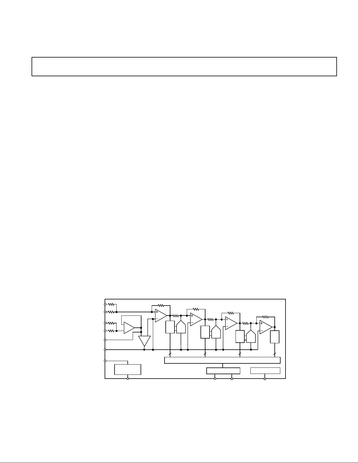
The AD1672 is a monolithic, single supply 12-bit, 3 MSPS
analog-to-digital converter with an on-chip, high performance
sample-and-hold amplifier (SHA) and voltage reference. The
AD1672 uses a multistage pipelined architecture with output
error correction logic to provide 12-bit accuracy at 3 MSPS data
rates and guarantees no missing codes over the full operating
temperature range. The AD1672 combines a high performance
BiCMOS process and a novel architecture to achieve its high
performance levels.
The fast settling input SHA is equally suited for both multiplexed systems that switch negative to positive full-scale voltage
levels in successive channels and sampling single-channel inputs
at frequencies up to the Nyquist rate. The AD1672’s wideband
Monolithic A/D Converter
AD1672
input combined with the power and cost savings over previously
available solutions will enable new designs in communications,
imaging and medical applications. The AD1672 provides both
reference output and reference input pins allowing the onboard
reference to serve as a system reference. An external reference
can also be chosen to suit the dc accuracy and temperature drift
requirements of the application. The digital output data is presented in a straight binary output format for the unipolar input
ranges of 0 V to 2.5 V and 0 V to 5.0 V. For the bipolar input
range of –2.5 V to +2.5 V, the digital output data is presented in
an offset binary format. An out-of-range (OTR) signal indicates
an overflow condition. It can be used with the most significant
bit to determine low or high overflow.
The AD1672 is packaged in a 28-pin PLCC package and is
specified for operation from –40°C to +85°C.
PRODUCT HIGHLIGHT
The AD1672 offers a complete single-chip sampling 12-bit,
3 MSPS analog-to-digital conversion function in a 28-pin
PLCC package.
The AD1672 at 240 mW consumes a fraction of the power of
presently available solutions and provides exceptional performance relative to other monolithic solutions.
OUT OF RANGE (OTR)—The OTR output bit indicates
when the input signal is beyond the AD1672’s input range.
Ease-of-Use—The single supply AD1672 is complete with SHA
voltage reference and pin strappable input ranges. It is compatible with a wide range of amplifiers.
FUNCTIONAL BLOCK DIAGRAM
AIN1 & 2
THA
ADC
4
REF IN
REFCOM
NOISE
REDUCTION
2.5V REF
OUTPUT
REF
AMP
DAC
AMP
BANDGAP
REFERENCE
REFCOM
REV. 0
Information furnished by Analog Devices is believed to be accurate and
reliable. However, no responsibility is assumed by Analog Devices for its
use, nor for any infringements of patents or other rights of third parties
which may result from its use. No license is granted by implication or
otherwise under any patent or patent rights of Analog Devices.
AD1672
THA
DAC
ADC
4
CORRECTION LOGIC
One Technology Way, P.O. Box 9106, Norwood. MA 02062-9106, U.S.A.
Tel: 617/329-4700 Fax: 617/326-8703
THA
DAC
LATCHES
OUTPUT DATA
12 BITS
ADC
3
DAC
CLOCK TIMER
CLOCK INPUT
THA
ADC
4
© Analog Devices, Inc., 1995

AD1672–SPECIFICATIONS
(T
to T
DC SPECIFICATIONS
MIN
with VCC = +5.0 V, VDD = +5.0 V, DRVDD = +5.0 V, f
MAX
AD1672AP
Parameter Min Typ Max Units
RESOLUTION 12 Bits
MAX CONVERSION RATE 3 MHz
ACCURACY
Integral Nonlinearity (INL) –2.5 ±1.0 2.5 LSB
Differential Nonlinearity (DNL) –1.0 ±0.5 1.5 LSB
No Missing Codes 12 Bits Guaranteed
Offset Error –0.75 ±0.20 0.75 % FSR
Zero Error
Gain Error
POWER SUPPLY REJECTION
V
CC
V
DD
V
DRDD
1
2
3
–0.75 ±0.20 0.75 % FSR
–1.50 ±0.30 1.50 % FSR
(5.0 V ± 0.25 V) –0.30 0.30 % FSR
(5.0 V ± 0.25 V) –0.30 0.30 % FSR
(3.0 V to 5.25 V) –0.10 0.10 % FSR
ANALOG INPUT
Input Ranges
2.5 V Range Unipolar 0.0 2.5 Volts
5.0 V Range Unipolar 0.0 5.0 Volts
5.0 V Bipolar –2.5 2.5 Volts
= 3 MHz unless otherwise noted)
SAMPLE
Input Resistance
2.5 V Input Range 1.5 2.0 2.5 kΩ
5.0 V Input Ranges 3.0 4.0 5.0 kΩ
Input Capacitance 10 pF
INTERNAL VOLTAGE REFERENCE
Output Voltage 2.475 2.5 2.525 Volts
Output Current
4
0.5 mA
REFERENCE INPUT RESISTANCE 6.0 8.0 10.0 kΩ
POWER SUPPLIES
Supply Voltages
V
CC
V
DD
DRV
DD
4.75 5.0 5.25 Volts
4.75 5.0 5.25 Volts
3.00 5.0 5.25 Volts
Supply Current
I
VCC
I
VDD
I
DRVDD
46 65 mA
1.0 2.0 mA
0.2 2.0 mA
POWER CONSUMPTION 240 363 mW
TEMPERATURE RANGE –40 25 85 °C
NOTES
1
Bipolar Mode.
2
Includes internal reference error.
3
Change in full scale as a function of the dc supply voltage.
4
Current available for external loads. External load should not change during conversion.
Specification subject to change without notice.
–2–
REV. 0

AD1672
(T
to T
with VCC = +5 .0 V, VDD = +5.0 V, DRVDD = +5.0 V, f
MAX
AC SPECIFICATIONS
MIN
–2.5 V to +2.5 V configuration unless otherwise noted)
AD1672AP
Parameter Min Typ Max Units
SIGNAL-TO-NOISE AND DISTORTION RATIO (S/(N+D))
f
= 100 kHz 68 dB
INPUT
f
= 500 kHz 63 68 dB
INPUT
f
= 1.5 MHz 60 dB
INPUT
SIGNAL-TO-NOISE RATIO (SNR)
f
= 100 kHz 70 dB
INPUT
f
= 500 kHz 66 70 dB
INPUT
f
= 1.5 MHz 67 dB
INPUT
TOTAL HARMONIC DISTORTION (THD)
f
= 100 kHz –74 dB
INPUT
f
= 500 kHz –74 –64 dB
INPUT
f
= 1.5 MHz –60 dB
INPUT
SPURIOUS FREE DYNAMIC RANGE (SFDR)
f
= 100 kHz –77 dB
INPUT
f
= 500 kHz –77 –65 dB
INPUT
f
= 1.5 MHz –61 dB
INPUT
INTERMODULATION DISTORTION (IMD)
1
65 dB
= 3 MHz, AIN = 0.5 dB in bipolar
SAMPLE
FULL POWER BANDWIDTH 5 MHz
SMALL SIGNAL BANDWIDTH (–20 dB FSR) 20 MHz
CODE TRANSITION NOISE 1/4 LSB rms
APERTURE DELAY 9 ns
APERTURE JITTER 10 ps rms
ACQUISITION TO FULL-SCALE STEP 150 ns
OVERVOLTAGE RECOVERY TIME 150 ns
NOTES
1
fs = 490 kHz; fb = 510 kHz typical value for third order products.
Specifications subject to change without notice.
(T
to T
DIGITAL SPECIFICATION
MIN
with VCC = +5 .0 V, VDD = +5.0 V, V
MAX
= +5.0 V unless otherwise noted)
DRVDD
AD1672AP
Parameter Symbol Min Typ Max Units
LOGIC INPUTS
High Level Input Voltage V
Low Level Input Voltage V
High Level Input Current (V
Low Level Input Current (V
= VDD)I
IN
= 0 V) I
IN
Input Capacitance C
IH
IL
IH
IL
IN
3.5 Volts
1.0 Volts
–10 10 µA
–10 10 µA
10 pF
LOGIC OUTPUTS
High Level Output Voltage (I
Low Level Output Voltage (I
Output Capacitance C
Specifications subject to change without notice.
= 0.5 mA) V
OH
= 1.6 mA) V
OL
OH
OL
OUT
2.4 Volts
0.4 Volts
5pF
REV. 0
–3–
AD1672
WARNING!
ESD SENSITIVE DEVICE
ANALOG
INPUT
INPUT
CLOCK
DATA
OUTPUT
OTR
S1
t
t
CH
S1
S2
C
t
CL
S2
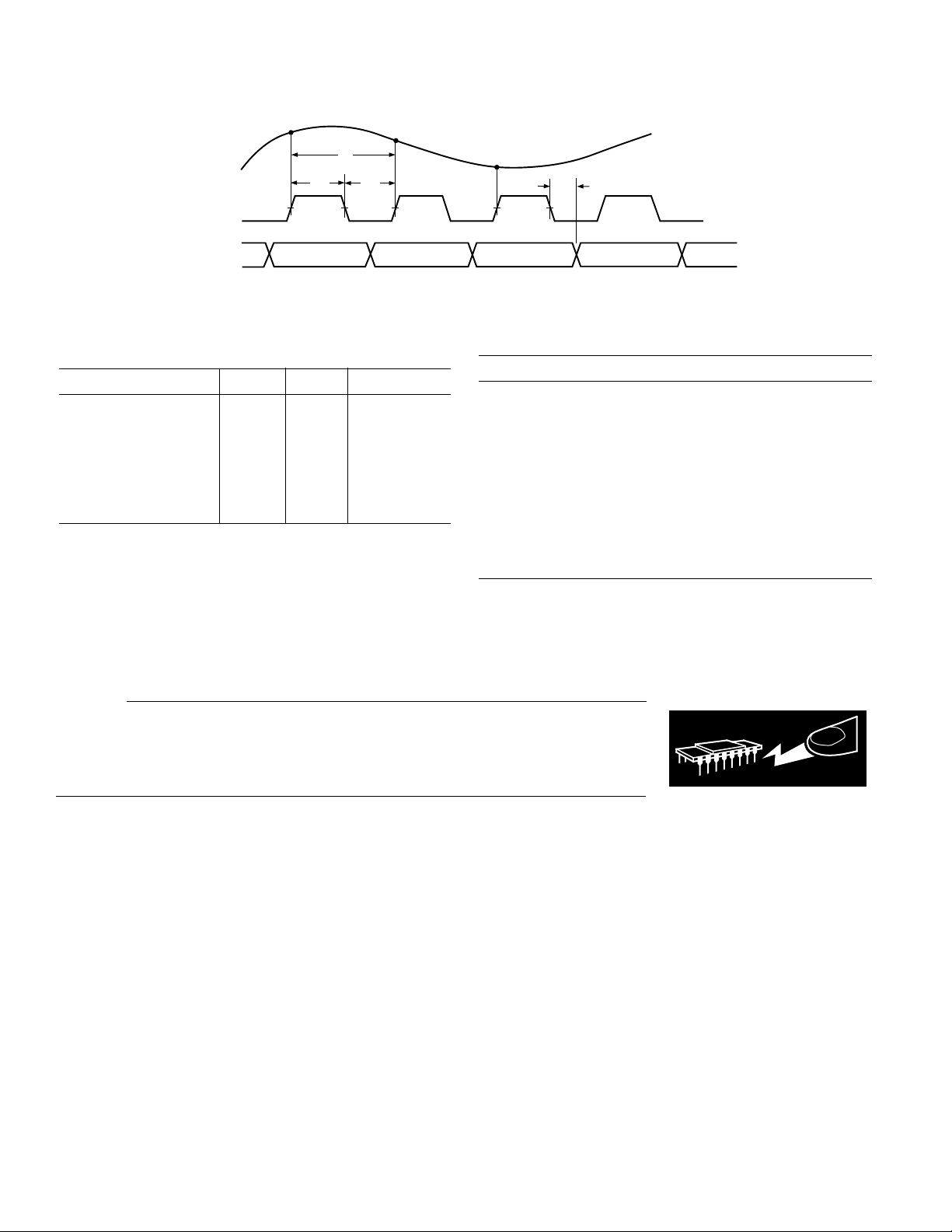
Figure 1. Timing Diagram
SWITCHING SPECIFICATIONS
Parameter Symbol Value Units
Clock Period t
C
Clock
Pulse Width High t
Pulse Width Low t
Output Delay t
CH
CL
OD
Pipeline Delay (Latency) 2.5 Clock Cycles
334 ns min
167 ns min
167 ns min
15 ns min
30 ns typ
S3
t
OD
S3
DATA 1
DATA 2
ABSOLUTE MAXIMUM RATINGS*
Parameter With Respect to Min Max Units
V
CC
V
DD
DRV
DD
ACOM –0 5 +6.5 Volts
DCOM –0.5 +6.5 Volts
DRCOM –0.5 +6.5 Volts
ACOM DCOM, DRCOM –0.5 +0.5 Volts
CLOCK DCOM –0.5 V
Digital Outputs DCOM –0.5 DRV
+ 0.5 Volts
DD
+ 0.5 Volts
DD
AIN ACOM –6.5 +6.5 Volts
REFIN ACOM –0.5 V
+ 0.5 Volts
CC
Junction Temperature +150 °C
Storage Temperature –65 +150 °C
Lead Temperature (10 sec) +300 °C
*Stresses above those listed under “Absolute Maximum Ratings” may cause
permanent damage to the device. This is a stress rating only and functional
operation of the device at these or any other conditions above those indicated in the
operational sections of this specification is not implied. Exposure to absolute
maximum ratings for extended periods may effect device reliability.
CAUTION
ESD (electrostatic discharge) sensitive device. Electrostatic charges as high as 4000 V readily
accumulate on the human body and test equipment and can discharge without detection.
Although the AD1672 features proprietary ESD protection circuitry, permanent damage may
occur on devices subjected to high energy electrostatic discharges. Therefore, proper ESD
precautions are recommended to avoid performance degradation or loss of functionality.
–4–
REV. 0
AD1672
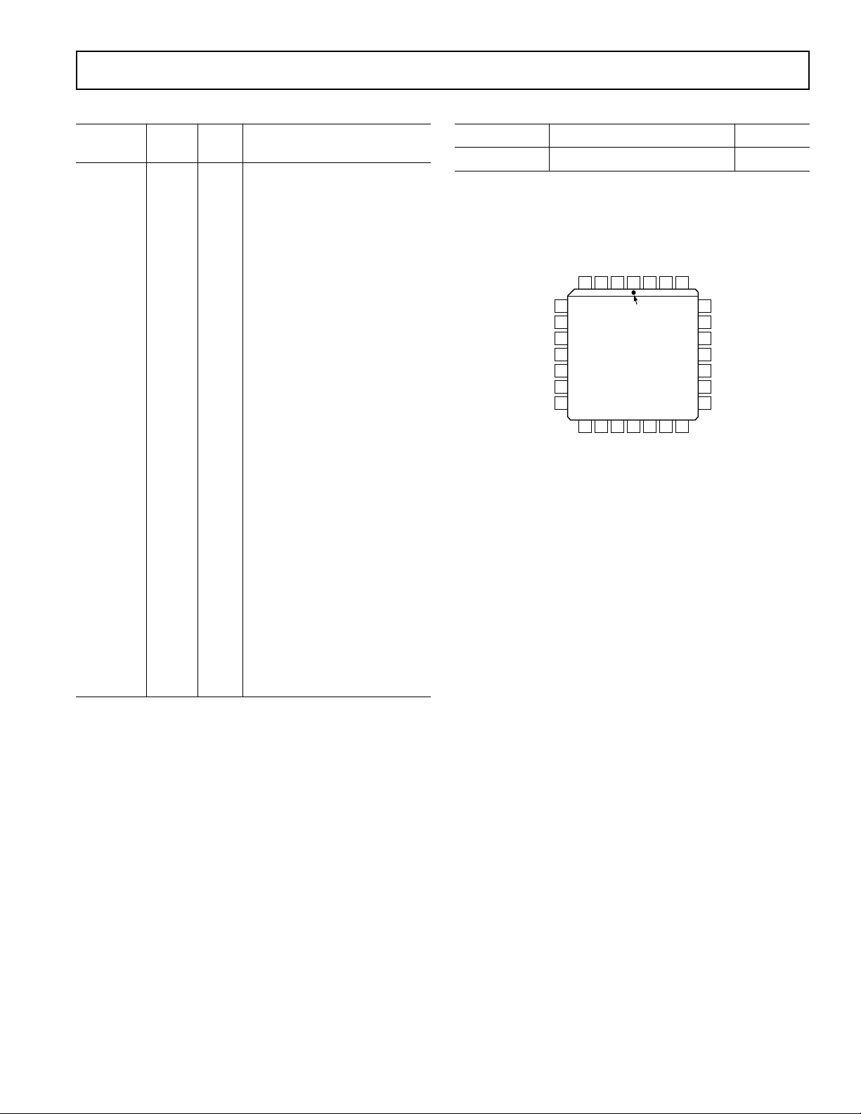
PIN DESCRIPTION
Pin
Symbol No. Type Name and Function
DRCOM 1 P Digital Output Driver Ground.
BIT 12 2 DO Data Bit (LSB).
BIT 2–11 3–12 DO Data Bits.
BIT 1 13 DO Data Bit (MSB).
DRV
DD
14 P +5 V Digital Output Driver Sup-
ply.
OTR 15 DO Out of Range is Active High on
the leading edge of Code 0 or the
trailing edge of Code 4096. See
Output Data Format Table V.
CLOCK 16 DI Sample Clock.
V
DD
17 P +5 V Digital Supply.
DCOM 18 P Digital Ground.
REFCOM 19, 24 P Analog Ground.
REFOUT 20 AO 2.5 V Reference Output
(Decouple with 1 µF ceramic
capacitor to REFCOM).
AIN1 21 AI Analog Input.
AIN2 22 AI Analog Input.
REFIN 23 AI Reference Input.
NCOMP2 25 AO Noise Compensation (Decouple
with 1 µF ceramic capacitor to
ACOM).
NCOMP1 26 AO Noise Compensation (Decouple
with 1 µF ceramic capacitor to
ACOM).
ACOM 27 P Analog Ground.
V
CC
TYPE: AI = Analog Input; DI = Digital Input; P = Power;
AO = Analog Output; DO = Digital Output.
28 P +5 V Analog Supply.
ORDERING GUIDE
Model Temperature Range Package
AD1672AP –40°C to +85°C P-28A
PIN CONFIGURATION
CC
ACOM
DRCOM
BIT 12 (LSB)
BIT 11
PIN 1
IDENTIFIER
AD1672
TOP VIEW
(Not to Scale)
DD
OTR
DRV
(MSB) BIT 1
V
28 27 261234
CLOCK
DD
V
NCOMP1
25
24
23
22
21
20
19
DCOM
NCOMP2
REFCOM
REFIN
AIN2
AIN1
REFOUT
REFCOM
BIT 9
BIT 8
BIT 7
BIT 6
BIT 5
BIT 4
BIT 3
BIT 10
5
6
7
8
9
10
11
121314 15 16 17 18
BIT 2
REV. 0
–5–

AD1672
DEFINITIONS OF SPECIFICATIONS
INTEGRAL NONLINEARITY ERROR (INL)
Integral nonlinearity error refers to the deviation of each individual
code from a line drawn from “negative full scale” through
“positive full scale.” The point used as “negative full scale”
occurs 1/2 LSB before the first code transition (all zeros to only
the LSB on). “Positive full scale” is defined as a level 1 1/2 LSB
beyond the last code transition (to all ones). The deviation is
measured from the middle of each particular code to the true
straight line.
DIFFERENTIAL LINEARITY ERROR (DNL, NO MISSING
CODES)
An ideal ADC exhibits code transitions that are exactly 1 LSB
apart. DNL is the deviation from this ideal value. Thus every
code must have a finite width. Guaranteed no missing codes to
12-bit resolution indicates that all 4096 codes must be present
over all operating ranges.
UNIPOLAR OFFSET ERROR
In the unipolar mode, the first transition should occur at a level
1/2 LSB above analog common. Unipolar offset is defines as
the deviation of the actual from that point.
BIPOLAR ZERO ERROR
In the bipolar mode, the major carry transition should occur for
an analog value 1/2 LSB below analog common. Zero error is
defined as the deviation of the actual transition from that point.
GAIN ERROR
The first transition should occur for an analog value 1/2 LSB
above nominal negative full scale. The last transition should
occur for an analog value 1 1/2 LSB below the nominal full
scale. Gain error is the deviation of the actual difference
between first and last code transitions and the ideal difference
between first and last code transitions.
APERTURE DELAY
Aperture delay is a measure of the Sample-and-Hold (SHA)
performance and is measured from the rising edge of the clock
input to when the input signal is held for conversion.
OVERVOLTAGE RECOVERY TIME
Overvoltage recovery time is defined as that amount of time
required for the ADC to achieve a specified accuracy after an
overvoltage (50% greater than full-scale range), measured from
the time the overvoltage signal reenters the converter’s range.
DYNAMIC SPECIFICATIONS
SIGNAL-TO-NOISE AND DISTORTION (S/N+D) RATIO
S/N+D is the ratio of the rms value of the measured input signal
to the rms sum of all other spectral components below the
Nyquist frequency, including harmonics but excluding dc. The
value for S/N+D is expressed in decibels.
TOTAL HARMONIC DISTORTION (THD)
THD is the ratio of the rms sum of the first six harmonic components to the rms value of the measured input signal and is
expressed as a percentage or in decibels.
INTERMODULATION DISTORTION (IMD)
With inputs consisting of sine waves at two frequencies, fa and
fb, any device with nonlinearities will create distortion products,
of order (m + n), at sum and difference frequencies of
mfa ± nfb, where m, n = 0, 1, 2, 3. . . . Intermodulation terms
are those for which m or n is not equal to zero. For example,
the second order terms are (fa + fb) and (fa – fb) and the third
order terms are (2 fa + fb), (2 fa – fb), (fa + 2fb) and (2 fb – fa).
The IMD products are expressed as the decibel ratio of the rms
sum of the measured input signals to the rms sum of the distortion terms. The two signals are of equal amplitude and the peak
value of their sums is –0.5 dB from full-scale. The IMD products are normalized to a 0 dB input signal.
POWER SUPPLY REJECTION
One of the effects of power supply error on the performance of
the device will be a small change in gain. The specifications
show the maximum change in the converter’s full scale as the
supplies are varied from minimum to maximum values.
APERTURE JITTER
Aperture jitter is the variation in aperture delay for successive
samples and is manifested as noise on the input to the A/D.
CODE TRANSITION NOISE
The effects of noise are to introduce an uncertainty in the precise determination of the analog input values at which the output code transitions take place, and, in effect, to increase or
reduce the quantization band. Code transition noise describes
the quantization band variation resulting from noise in terms of
rms LSBs.
–6–
FULL-POWER BANDWIDTH
The full-power bandwidth is that input frequency at which the
amplitude of the reconstructed fundamental is reduced by 3 dB
for a full-scale input.
SPURIOUS FREE DYNAMIC RANGE
The difference, in dB, between the rms amplitude of the input
signal and the peak spurious signal.
REV. 0
 Loading...