

2.5 V to 5.0 V Micropower, Precision
a
AD1582/AD1583/AD1584/AD1585
FEATURES
Series Reference (2.5 V, 3 V, 4.096 V, 5 V)
Initial Accuracy: ⴞ0.1% max
Temperature Drift: ⴞ50 ppm/ⴗC max
Low Quiescent Current: 65 A max
Current Output Capability: ⴞ5 mA
Wide Supply Range: V
IN
= V
Wideband Noise (10 Hz–10 kHz): 50 V rms
Operating Temperature Range: –40ⴗC to +85ⴗC
Compact, Surface-Mount, SOT-23 Package
GENERAL DESCRIPTION
The AD1582, AD1583, AD1584 and AD1585 are a family of
low cost, low power, low dropout, precision bandgap references.
These designs are available as three-terminal (series) devices and
are packaged in the compact SOT-23, 3-pin, surface mount
package. The versatility of these references makes them ideal for
use in battery powered 3 V or 5 V systems where there may be
wide variations in supply voltage and a need to minimize power
dissipation.
The superior accuracy and temperature stability of the AD1582/
AD1583/AD1584/AD1585 is made possible by the precise
matching and thermal tracking of on-chip components. Patented
temperature drift curvature correction design techniques have
been used to minimize the nonlinearities in the voltage output
temperature characteristic.
These series mode devices (AD1582/AD1583/AD1584/AD1585)
will source or sink up to 5 mA of load current and operate
efficiently with only 200 mV of required headroom. This family
will draw a maximum 65 µA of quiescent current with only a
1.0 µA/V variation with supply voltage. The advantage of these
designs over conventional shunt devices is extraordinary. Valuable
supply current is no longer wasted through an input series
resistor and maximum power efficiency is achieved at all input
voltage levels.
The AD1582, AD1583, AD1584 and AD1585 are available in
two grades, A and B, both of which are provided in the smallest
available package on the market, the SOT-23. Both grades are
specified over the industrial temperature range of –40°C to
+85°C.
+ 200 mV to 12 V
OUT
Series Mode Voltage References
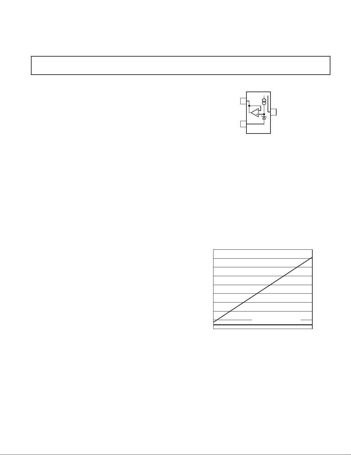
FUNCTIONAL BLOCK DIAGRAM
1
V
OUT
3
V
IN
2
GND
AD1582/3/4/5
TOP VIEW
TARGET APPLICATIONS
1. Portable, Battery Powered Equipment. Notebook Computers, Cellular Phones, Pagers, PDAs, GPSs and DMMs.
2. Computer Workstations. Suitable for use with a wide range
of video RAMDACs.
3. Smart Industrial Transmitters.
4. PCMCIA Cards.
5. Automotive.
6. Hard Disk Drives.
7. 3 V/5 V 8-Bit–12-Bit Data Converters.
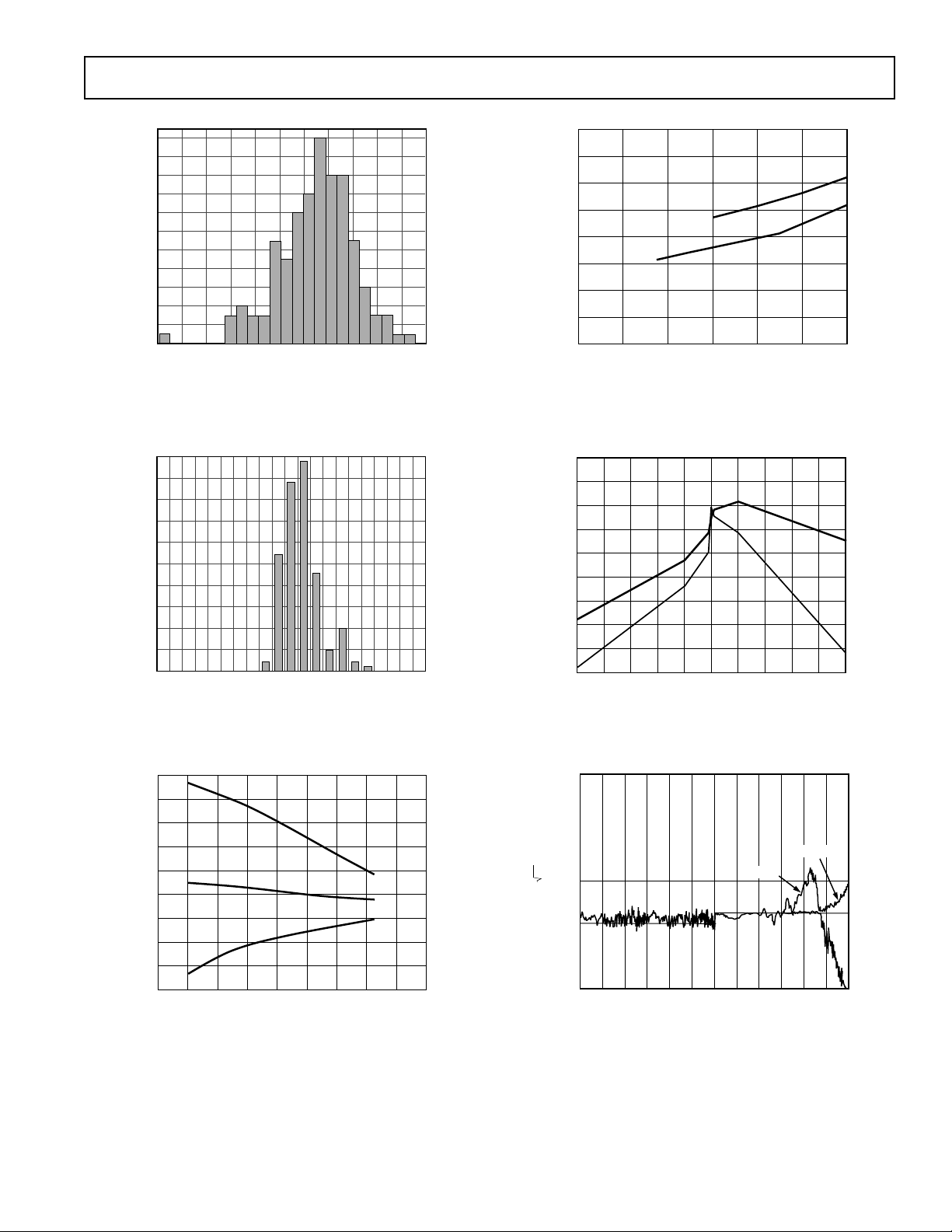
900
800
700
600
500
– A
400
SUPPLY
I
300
200
100
0
2.7 5
Figure 1. Supply Current (µA) vs. Supply Voltage (V)
SHUNT REFERENCE*
AD1582 SERIES REFERENCE
V
– V
SUPPLY
*3.076k⍀ SOURCE RESISTOR
REV. A
Information furnished by Analog Devices is believed to be accurate and
reliable. However, no responsibility is assumed by Analog Devices for its
use, nor for any infringements of patents or other rights of third parties
which may result from its use. No license is granted by implication or
otherwise under any patent or patent rights of Analog Devices.
One Technology Way, P.O. Box 9106, Norwood, MA 02062-9106, U.S.A.
Tel: 781/329-4700 World Wide Web Site: http://www.analog.com
Fax: 781/326-8703 © Analog Devices, Inc., 2000

AD1582/AD1583/AD1584/AD1585
AD1582–SPECIFICATIONS
(@ TA = T
, VIN = 5 V, unless otherwise noted)
MIN–TMAX
Model AD1582A AD1582B
Min Typ Max Min Typ Max Units
OUTPUT VOLTAGE (@ +25°C) 2.48 2.50 2.52 2.498 2.500 2.502 V
OUT
1
100 50 ppm/°C
)
OUTPUT VOLTAGE TEMPERATURE DRIFT
MINIMUM SUPPLY HEADROOM (VIN–V
With I
= 1 mA 200 200 mV
OUT
LOAD REGULATION
0 mA < I
–5 mA < I
< 5 mA 200 200 µV/mA
OUT
< 0 mA 250 250 µV/mA
OUT
LOAD REGULATION
–100 µA < I
< 100 µA 2 2 mV/mA
OUT
LINE REGULATION
+200 mV < VIN < 12 V
V
OUT
I
= 0 mA 25 25 µV/V
OUT
RIPPLE REJECTION (∆V
VIN = 5 V ± 100 mV (f = 120 Hz)
OUT
/∆VIN)
2
80 80 dB
QUIESCENT CURRENT 65 65 µA
SHORT CIRCUIT CURRENT TO GROUND 15 15 mA
NOISE VOLTAGE (@ +25°C)
0.1 Hz to 10 Hz 70 70 µV p-p
10 Hz to 10 kHz 50 50 µV rms
TURN-ON SETTLING TIME TO 0.1%
LONG-TERM STABILITY
1000 Hours @ +25°C
4
OUTPUT VOLTAGE HYSTERESIS
3
100 100 µs
100 100 ppm/1000 hrs.
5
115 115 ppm
TEMPERATURE RANGE
Specified Performance (A, B) –40 +85 –40 +85 °C
Operating Performance (A, B)
NOTES
1
Maximum output voltage drift is guaranteed for all grades.
2
Ripple Rejection over a wide frequency spectrum is shown in Figure 15.
3
Measured with a capacitance load of 0.2 µF.
4
Long-term stability at +125°C = 1600 ppm/1000 hours.
5
Hysteresis is defined as the change in the 25°C output voltage, caused by bringing the device to +85 °C, taking a 25°C measurement and then bringing it to –40°C, followed
by another 25°C measurement. Refer to Figure 12.
6
The operating temperature range is defined as the temperature extremes at which the device will still function. Parts may deviate from their specified performance outside
the specified temperature range.
Specifications subject to change without notice.
6
–55 +125 –55 +125 °C
–2–
REV. A

AD1582/AD1583/AD1584/AD1585
AD1583–SPECIFICATIONS
(@ TA = T
, VIN = 5 V, unless otherwise noted)
MIN–TMAX
Model AD1583A AD1583B
Min Typ Max Min Typ Max Units
OUTPUT VOLTAGE (@ +25°C) 2.97 3.00 3.03 2.997 3.000 3.003 V
OUTPUT VOLTAGE TEMPERATURE DRIFT
MINIMUM SUPPLY HEADROOM (V
With I
= 1 mA 200 200 mV
OUT
IN–VOUT
1
100 50 ppm/°C
)
LOAD REGULATION
0 mA < I
–5 mA < I
< 5 mA 250 250 µV/mA
OUT
< 0 mA 400 400 µV/mA
OUT
LOAD REGULATION
–100 µA < I
< 100 µA 2.4 2.4 mV/mA
OUT
LINE REGULATION
+200 mV < VIN < 12 V
V
OUT
I
= 0 mA 25 25 µV/V
OUT
RIPPLE REJECTION (∆V
VIN = 5 V ± 100 mV (f = 120 Hz)
OUT
/∆VIN)
2
80 80 dB
QUIESCENT CURRENT 65 65 µA
SHORT CIRCUIT CURRENT TO GROUND 15 15 mA
NOISE VOLTAGE (@ +25°C)
0.1 Hz to 10 Hz 85 85 µV p-p
10 Hz to 10 kHz 60 60 µV rms
TURN-ON SETTLING TIME TO 0.1%
3
120 120 µs
LONG-TERM STABILITY
1000 Hours @ +25°C 100 100 ppm/1000 hrs.
OUTPUT VOLTAGE HYSTERESIS
4
115 115 ppm
TEMPERATURE RANGE
Specified Performance (A, B) –40 +85 –40 +85 °C
Operating Performance (A, B)
NOTES
1
Maximum output voltage drift is guaranteed for all grades.
2
Ripple Rejection over a wide frequency spectrum is shown in Figure 15.
3
Measured with a capacitance load of 0.2 µF.
4
Hysteresis is defined as the change in the 25°C output voltage, caused by bringing the device to +85 °C, taking a 25°C measurement and then bringing it to –40°C, followed
by another 25°C measurement. Refer to Figure 12.
5
The operating temperature range is defined as the temperature extremes at which the device will still function. Parts may deviate from their specified performance outside
the specified temperature range.
Specifications subject to change without notice.
5
–55 +125 –55 +125 °C
REV. A
–3–

AD1582/AD1583/AD1584/AD1585
AD1584–SPECIFICATIONS
(@ TA = T
, VIN = 5 V, unless otherwise noted)
MIN–TMAX
Model AD1584A AD1584B
Min Typ Max Min Typ Max Units
OUTPUT VOLTAGE (@ +25°C) 4.056 4.096 4.136 4.092 4.096 4.100 V
OUTPUT VOLTAGE TEMPERATURE DRIFT
MINIMUM SUPPLY HEADROOM (V
With I
= 1 mA 200 200 mV
OUT
IN–VOUT
1
100 50 ppm/°C
)
LOAD REGULATION
0 mA < I
–5 mA < I
< 5 mA 320 320 µV/mA
OUT
< 0 mA 320 320 µV/mA
OUT
LOAD REGULATION
–100 µA < I
< 100 µA 3.2 3.2 mV/mA
OUT
LINE REGULATION
+200 mV < VIN < 12 V
V
OUT
I
= 0 mA 25 25 µV/V
OUT
RIPPLE REJECTION (∆V
VIN = 5 V ± 100 mV (f = 120 Hz)
OUT
/∆VIN)
2
80 80 dB
QUIESCENT CURRENT 65 65 µA
SHORT CIRCUIT CURRENT TO GROUND 15 15 mA
NOISE VOLTAGE (@ +25°C)
0.1 Hz to 10 Hz 110 110 µV p-p
10 Hz to 10 kHz 90 90 µV rms
TURN-ON SETTLING TIME TO 0.1%
3
140 140 µs
LONG-TERM STABILITY
1000 Hours @ +25°C 100 100 ppm/1000 hrs.
OUTPUT VOLTAGE HYSTERESIS
4
115 115 ppm
TEMPERATURE RANGE
Specified Performance (A, B) –40 +85 –40 +85 °C
Operating Performance (A, B)
NOTES
1
Maximum output voltage drift is guaranteed for all grades.
2
Ripple Rejection over a wide frequency spectrum is shown in Figure 15.
3
Measured with a capacitance load of 0.2 µF.
4
Hysteresis is defined as the change in the 25°C output voltage, caused by bringing the device to +85 °C, taking a 25°C measurement and then bringing it to –40°C, followed
by another 25°C measurement. Refer to Figure 12.
5
The operating temperature range is defined as the temperature extremes at which the device will still function. Parts may deviate from their specified performance outside
the specified temperature range.
Specifications subject to change without notice.
5
–55 +125 –55 +125 °C
–4–
REV. A

AD1582/AD1583/AD1584/AD1585
AD1585–SPECIFICATIONS
(@ TA = T
, VIN = 6 V, unless otherwise noted)
MIN–TMAX
Model AD1585A AD1585B
Min Typ Max Min Typ Max Units
OUTPUT VOLTAGE (@ +25°C) 4.95 5.00 5.05 4.995 5.000 5.005 V
OUTPUT VOLTAGE TEMPERATURE DRIFT
MINIMUM SUPPLY HEADROOM (V
With I
= 1 mA 200 200 mV
OUT
IN–VOUT
1
100 50 ppm/°C
)
LOAD REGULATION
0 mA < I
–5 mA < I
< 5 mA 400 400 µV/mA
OUT
< 0 mA 400 400 µV/mA
OUT
LOAD REGULATION
–100 µA < I
< 100 µA 4 4 mV/mA
OUT
LINE REGULATION
+200 mV < VIN < 12 V
V
OUT
I
= 0 mA 25 25 µV/V
OUT
RIPPLE REJECTION (∆V
VIN = 6 V ± 100 mV (f = 120 Hz)
OUT
/∆VIN)
2
80 80 dB
QUIESCENT CURRENT 65 65 µA
SHORT CIRCUIT CURRENT TO GROUND 15 15 mA
NOISE VOLTAGE (@ +25°C)
0.1 Hz to 10 Hz 140 140 µV p-p
10 Hz to 10 kHz 100 100 µV rms
TURN-ON SETTLING TIME TO 0.1%
3
175 175 µs
LONG-TERM STABILITY
1000 Hours @ +25°C 100 100 ppm/1000 hrs.
OUTPUT VOLTAGE HYSTERESIS
4
115 115 ppm
TEMPERATURE RANGE
Specified Performance (A, B) –40 +85 –40 +85 °C
Operating Performance (A, B)
NOTES
1
Maximum output voltage drift is guaranteed for all grades.
2
Ripple Rejection over a wide frequency spectrum is shown in Figure 15.
3
Measured with a capacitance load of 0.2 µF.
4
Hysteresis is defined as the change in the 25°C output voltage, caused by bringing the device to +85 °C, taking a 25°C measurement and then bringing it to –40°C, followed
by another 25°C measurement. Refer to Figure 12.
5
The operating temperature range is defined as the temperature extremes at which the device will still function. Parts may deviate from their specified performance outside
the specified temperature range.
Specifications subject to change without notice.
5
–55 +125 –55 +125 °C
REV. A
–5–

AD1582/AD1583/AD1584/AD1585
ABSOLUTE MAXIMUM RATINGS
VIN to Ground . . . . . . . . . . . . . . . . . . . . . . . . . . . . . . . . . 12 V
Internal Power Dissipation
2
1
SOT-23 (RT) . . . . . . . . . . . . . . . . . . . . . . . . . . . . . 400 mW
Storage Temperature Range . . . . . . . . . . . . –65°C to +125°C
Operating Temperature Range
AD1582/AD1583/AD1584/AD1585RT . . . –40°C to +85°C
Lead Temperature, Soldering
Vapor Phase (60 sec) . . . . . . . . . . . . . . . . . . . . . . . . +215°C
Infrared (15 sec) . . . . . . . . . . . . . . . . . . . . . . . . . . . . .+220°C
NOTES
1
Stresses above those listed under Absolute Maximum Ratings may cause
permanent damage to the device. This is a stress rating only; functional operation
of the device at these or any other conditions above those indicated in the
operational section of this specification is not implied. Exposure to absolute
maximum rating conditions for extended periods may affect device reliability.
2
Specification is for device in free air at 25°C: SOT-23 Package: θJA = 300°C/W.
ORDERING GUIDE
1
Model
AD1582/AD1583/AD1584/AD1585ART 1.0% 100 ppm/°C
AD1582/AD1583/AD1584/AD1585ARTRL
AD1582/AD1583/AD1584/AD1585ARTRL7
AD1582/AD1583/AD1584/AD1585BRT 0.1% 50 ppm/°C
AD1582/AD1583/AD1584/AD1585BRTRL
AD1582/AD1583/AD1584/AD1585BRTRL7
NOTES
1
Package Option for all Models; RT = Surface Mount, SOT-23.
2
Provided on a 13-inch reel containing 10,000 pieces.
3
Provided on a 7-inch reel containing 3,000 pieces.
2
3
2
3
PACKAGE BRANDING INFORMATION
Four marking fields identify the device generic, grade and date
of processing. The first field is the product identifier. A “2/3/4/5”
identifies the generic as the AD1582/3/4/5. The second field
indicates the device grade; “A” or “B.” In the third field a
numeral or letter indicates the calendar year; “7” for 1997. . . ,
“A” for 2001. . . The fourth field uses letters A-Z to represent a
two week window within the calendar year, starting with “A” for
the first two weeks of January.
Initial Output Temperature
Error Coefficient
1.0% 100 ppm/°C
1.0% 100 ppm/°C
0.1% 50 ppm/°C
0.1% 50 ppm/°C
CAUTION
ESD (electrostatic discharge) sensitive device. Electrostatic charges as high as 4000 V readily
accumulate on the human body and test equipment and can discharge without detection.
Although the AD1582/AD1583/AD1584/AD1585 feature proprietary ESD protection circuitry,
permanent damage may occur on devices subjected to high energy electrostatic discharges.
Therefore, proper ESD precautions are recommended to avoid performance degradation or loss
of functionality.
–6–
REV. A
Typical Performance Characteristics–
VIN – Volts
024681012
0
0.25
0.20
0.15
0.10
0.35
0.30
0.40
0.05
1585
1582
mV/mA
22
20
18
16
14
12
10
# OF PARTS
8
6
4
2
0
–60 50–50 –10 10
–40 –30 –20 0 20
ppm/ⴗC
Figure 2. Typical Output Voltage Temperature Drift
Distribution
30
40
AD1582/AD1583/AD1584/AD1585
Figure 5. Load Regulation vs. V
IN
50
45
40
35
30
25
# OF PARTS
20
15
10
5
0
–100% 1.00%–0.60% –0.20% 0.20% 0.60%
V
OUT
– ERROR
Figure 3. Typical Output Voltage Error Distribution
2.510
2.508
2.506
2.504
2.502
OUT
V
2.500
2.498
2.496
2.494
2.492
–60 120–40 –20 0 20 40 60 80 100
TEMPERATURE – ⴗC
Figure 4. Typical Temperature Drift Characteristic Curves
0
–10
–20
–30
–40
V/V
–50
–60
–70
–80
–90
–51–4 –3 –2 –10 23 45
Figure 6. Line Regulation vs. I
1E+04
1E+03
nV/ Hz
1E+02
1582
1585
I
– mA
OUT
1E+031E+021E+01
FREQUENCY – Hz
I
OUT
LOAD
I
= 0
1E+04
Figure 7. Noise Spectral Density
OUT
= 1mA
1E+05
REV. A
–7–

AD1582/AD1583/AD1584/AD1585
THEORY OF OPERATION
The AD1582/AD1583/AD1584/AD1585 family uses the
“bandgap” concept to produce stable, low temperature coefficient voltage references suitable for high accuracy data acquisition components and systems. This family of precision references
makes use of the underlying temperature characteristics of a
silicon transistor’s base-emitter voltage in the forward biased
operating region. Under this condition, all such transistors have
a –2 mV/°C temperature coefficient (TC) and a V
extrapolated to absolute zero, 0°K, (with collector current proportional to absolute temperature) approximates the silicon bandgap
voltage. By summing a voltage that has an equal and opposite
temperature coefficient of +2 mV/°C with the VBE of a forwardbiased transistor, a zero TC reference can be developed. In the
AD1582/AD1583/AD1584/AD1585 simplified circuit diagram
shown in Figure 8, such a compensating voltage, V1, is derived
by driving two transistors at different current densities and
amplifying the resultant V
positive TC). The sum (V
difference (∆VBE—which has a
BE
) of VBE and V1 is then buffered
BG
and amplified to produce stable reference voltage outputs of
2.5 V, 3 V, 4.096 V, and 5 V.
R3
+
V
R2
BE
–
R1
R4
+
V1
–
Figure 8. Simplified Schematic
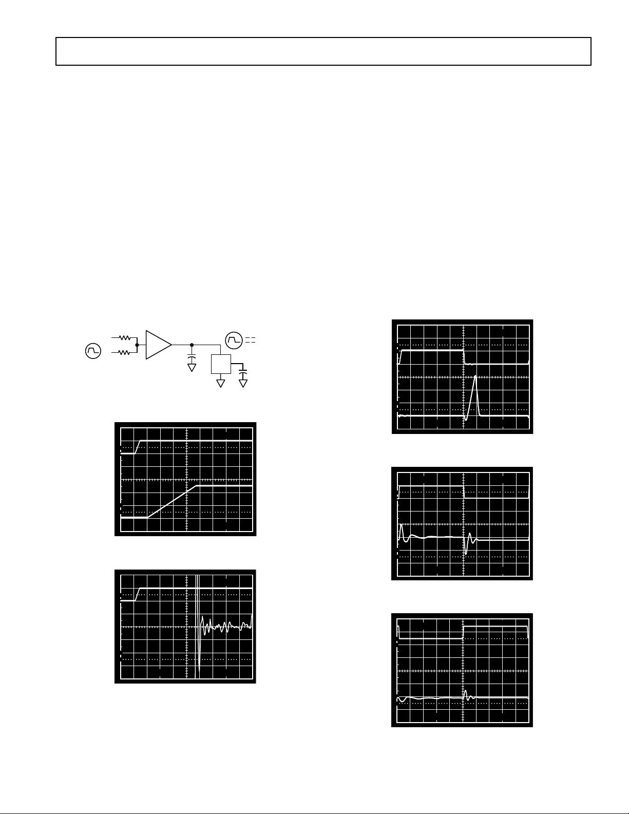
APPLYING THE AD1582/AD1583/AD1584/AD1585
The AD1582/AD1583/AD1584/AD1585 is a family of series
references that can be utilized for many applications. To achieve
optimum performance with these references, only two external
components are required. Figure 9 shows the AD1582 configured for operation under all loading conditions. With a simple
4.7 µF capacitor attached to the input and a 1 µF capacitor
applied to the output, the devices will achieve specified performance for all input voltage and output current requirements.
For best transient response, add a 0.1 µF capacitor in parallel with
the 4.7 µF. While a 1 µF output capacitor will provide stable
performance for all loading conditions, the AD1582 can operate
under low (–100 µA < I
< 100 µA) current conditions with
OUT
just a 0.2 µF output capacitor. The 4.7 µF capacitor on the input
can be reduced to 1 µF in this condition.
Unlike conventional shunt reference designs, the AD1582/
AD1583/AD1584/AD1585 family provides stable output
voltages at constant operating current levels. When properly
decoupled, as shown in Figure 9, these devices can be applied to
any circuit and provide superior low power solutions.
that, when
BE
V
V
OUT
R5
V
BG
R6
GND
IN
+
V
OUT
–
1F
1
3
2
4.7F
V
IN
Figure 9. Typical Connection Diagram
TEMPERATURE PERFORMANCE
The AD1582/AD1583/AD1584/AD1585 family of references is
designed for applications where temperature performance is
important. Extensive temperature testing and characterization
ensures that the device’s performance is maintained over the
specified temperature range.
Some confusion exists, however, in the area of defining and
specifying reference voltage error over temperature. Historically,
references have been characterized using a maximum deviation
per degree centigrade, i.e., 50 ppm/°C. However, because of the
inconsistent nonlinearities in standard zener references (such as
“S” type characteristics), most manufacturers use a maximum
limit error band approach to characterize their references. Using
this technique, the voltage reference output voltage error band is
specified by taking output voltage measurements at three or
more different temperatures.
The error band guaranteed with the AD1582/AD1583/AD1584/
AD1585 family is the maximum deviation from the initial value
at +25°C; this method is of more use to a designer than the one
which simply guarantees the maximum error band over the
entire temperature change. Thus, for a given grade of the
AD1582/AD1583/AD1584/AD1585, the designer can easily
determine the maximum total error by summing initial accuracy
and temperature variation (e.g., for the AD1582BRT, the initial
tolerance is ± 2 mV, the temperature error band is ±8 mV, thus
the reference is guaranteed to be 2.5 V ± 10 mV from –40°C to
+85°C).
Figure 10 shows the typical output voltage drift for the AD1582
and illustrates the methodology. The box in Figure 10 is bounded
on the x-axis by operating temperature extremes, and on the yaxis by the maximum and minimum output voltages observed
over the operating temperature range. The slope of the diagonal
drawn from the initial output value at +25°C to the output
values at +85°C and –40°C determines the performance grade
of the device.
Duplication of these results requires a test system that is highly
accurate with stable temperature control. Evaluation of the
AD1582 will produce curves similar to those in Figures 4 and
10, but output readings may vary depending upon the test
methods and test equipment utilized.
–8–
REV. A

AD1582/AD1583/AD1584/AD1585
pp
2.510
2.509
2.508
2.507
2.506
– Volts
2.505
OUT
V
2.504
2.503
2.502
2.501
–60 120–40 –200 20406080100
TEMPERATURE – ⴗC
Figure 10. Output Voltage vs. Temperature
VOLTAGE OUTPUT NONLINEARITY VS. TEMPERATURE
When using a voltage reference with data converters, it is
important to understand the impact that temperature drift can
have on the converter’s performance. The nonlinearity of the
reference output drift represents additional error that cannot
easily be calibrated out of the overall system. To better understand the impact such a drift can have on a data converter, refer
to Figure 11 where the measured drift characteristic is normalized to the end point average drift. The residual drift error of the
AD1582 of approximately 200 ppm demonstrates that this
family of references is compatible with systems that require
12-bit accurate temperature performance.
250
200
150
hysteresis, the AD1582/AD1583/AD1584/AD1585 family
is designed to minimize this characteristic. This phenomenon can be quantified by measuring the change in the
+25°C output voltage after temperature excursions from
+85°C to +25°C, and –40°C to +25°C. Figure 12 displays
the distribution of the AD1582 output voltage hysteresis.
80
70
60
50
40
# OF PARTS
30
20
10
0
–700 –450 –200 50 300 550
m
Figure 12. Output Voltage Hysteresis Distribution
SUPPLY CURRENT VS. TEMPERATURE
The quiescent current for the AD1582/AD1583/AD1584/
AD1585 family of references will vary slightly over temperature and input supply range. Figure 13 demonstrates the
typical performance for the AD1582 reference when varying
both temperature and supply voltage. As is evident from the
graph, the AD1582 supply current increases only 1.0 µA/V,
making this device extremely attractive for use in applications where there may be wide variations in supply voltage
and a need to minimize power dissipation.
100
100
⌬ – ppm
OUT
V
50
0
–50
–50 100–250 255075
TEMPERATURE – ⴗC
Figure 11. Residual Drift Error
OUTPUT VOLTAGE HYSTERESIS
High performance industrial equipment manufacturers may
require the AD1582/AD1583/AD1584/AD1585 family to
maintain a consistent output voltage error at +25°C after the
references are operated over the full temperature range. While
all references exhibit a characteristic known as output voltage
80
60
– A
Q
I
40
20
0
34567891011
TA = 85ⴗC
TA = –40ⴗC
V
IN
TA = 25ⴗC
– Volts
Figure 13. Typical Supply Current over Temperature
REV. A
–9–

AD1582/AD1583/AD1584/AD1585
AC PERFORMANCE
To successfully apply the AD1582/AD1583/AD1584/AD1585
family of references, it is important to understand the effects of
dynamic output impedance and power supply rejection. In
Figure 14a, a voltage divider is formed by the AD1582’s output
impedance and the external source impedance. Figure 14b
shows the effect of varying the load capacitor on the reference
output. Power supply rejection ratio (PSRR) should be determined when characterizing the ac performance of a series
voltage reference. Figure 15a shows a test circuit used to
measure PSRR, and Figure 15b demonstrates the AD1582’s
ability to attenuate line voltage ripple.
V
DC
2X V
ⴞ2V
OUT
10k⍀
10k⍀
X1
ⴞ100A
LOAD
10k⍀
1F
2k⍀
5V
DUT
5F
Figure 14a. Output Impedance Test Circuit
100
1F CAP
10
1585
OHM
1
1582
100
90
80
70
60
50
40
PSRR – dB
30
20
10
0
1.E+00 1.E+061.E+01 1.E+02 1.E+03 1.E+04 1.E+05
FREQUENCY – Hz
1582
1585
Figure 15b. Ripple Rejection vs. Frequency
NOISE PERFORMANCE AND REDUCTION
The noise generated by the AD1582 is typically less then
70 µV p-p over the 0.1 Hz to 10 Hz frequency band. Figure 16
shows the 0.1 Hz to 10 Hz noise of a typical AD1582. The noise
measurement is made with a high gain bandpass filter. Noise in
a 10 Hz to 10 kHz region is approximately 50 µV rms. Figure 17
shows the broadband noise of a typical AD1582. If further noise
reduction is desired, a 1-pole low-pass filter may be added
between the output pin and ground. A time constant of 0.2 ms
will have a –3 dB point at roughly 800 Hz, and will reduce the
high frequency noise to about 16 µV rms. It should be noted,
however, that while additional filtering on the output may improve
the noise performance of the AD1582/AD1583/AD1584/AD1585
family, the added output impedance could degrade the ac
performance of the references.
0.1
1E+01 1E+02 1E+03 1E+04 1E+05 1E+06
FREQUENCY – Hz
Figure 14b. Output Impedance vs. Frequency
10V
ⴞ200mV
10k
X1
⍀
0.22
F
5V ⴞ100mV
DUT
V
OUT
0.22F
⍀
10k
Figure 15a. Ripple Rejection Test Circuit
10V 1s
100
90
10
0%
Figure 16. 0.1–10 Hz Voltage Noise
100V
100
90
10
0%
10ms
Figure 17. 10 Hz to 10 kHz Wideband Noise
–10–
REV. A
AD1582/AD1583/AD1584/AD1585
TURN-ON TIME
Many low power instrument manufacturers are becoming
increasingly concerned with the turn-on characteristics of the
components being used in their systems. Fast turn-on components often enable the end user to save power by keeping power
off when it is not needed. Turn-on settling time is defined as the
time required, after the application of power (cold start), for the
output voltage to reach its final value within a specified error.
The two major factors affecting this are the active circuit settling
time and the time required for the thermal gradients on the chip
to stabilize. Figure 18a shows the turn-on settling and transient
response test circuit. Figure 18b displays the turn-on characteristic of the AD1582. This characteristic is generated from coldstart operation and represents the true turn-on waveform after
power up. Figure 18c shows the fine settling characteristics of
the AD1582. Typically, the reference settles to within 0.1% of
its final value in about 100 µs.
The device can momentarily draw excessive supply current
when V
is slightly below the minimum specified level.
SUPPLY
Power supply resistance must be low enough to ensure reliable
turn-on. Fast power supply edges minimize this effect.
0V OR 10V
0V TO 10V
10k⍀
10k⍀
X1
0.22F
DUT
V
OUT
5V OR 10V
0V OR 5V
0.22F
DYNAMIC PERFORMANCE
Many A/D and D/A converters present transient current loads
to the reference, and poor reference response can degrade the
converter’s performance. The AD1582/3/4/5 family of references has been designed to provide superior static and dynamic
line and load regulation. Since these series references are
capable of both sourcing and sinking large current loads, they
exhibit excellent settling characteristics.
Figure 19 displays the line transient response for the AD1582.
The circuit utilized to perform such a measurement is displayed
in Figure 18a, where the input supply voltage is toggled from
5 V to 10 V and the input and output capacitors are each 0.22 µF.
Figures 20 and 21 show the load transient settling characteristics for the AD1582 when load current steps of 0 mA to 5 mA
and 0 mA to –1 mA are applied. The input supply voltage
remains constant at 5 V, the input decoupling and output load
capacitors are 4.7 µF and 1 µF respectively, and the output current
is toggled. For both positive and negative current loads, the
reference responses settle very quickly and exhibit initial voltage
spikes less than 10 mV.
5V
100
90
50s
Figure 18a. Turn-On/Transient Response Test Circuit
5V
100
90
10
0%
1V
20s
20s
Figure 18b. Turn-On Characteristics
5V
100
90
10
0%
1mV
20s
20s
Figure 18c. Turn-On Settling
10
0%
200mV
50s
Figure 19. Line Transient Response
5V
100
90
10
0%
5mV
20s
20s
Figure 20. Load Transient Response (0 mA to 5 mA Load)
5V
100
90
10
0%
5mV
20s
20s
REV. A
Figure 21. Load Transient Response
(0 mA to –1 mA Load)
–11–

AD1582/AD1583/AD1584/AD1585
Dimensions shown in inches and (mm).
OUTLINE DIMENSIONS
Surface Mount Package
SOT-23
0.1200 (3.048)
0.1102 (2.799)
8.0
ⴞ 0.30
1.5
+0.05
–0.00
4.0 ⴞ 0.10
0.0470 (1.194)
0.0236 (0.599)
0.0177 (0.450)
0.0040 (0.102)
0.0005 (0.013)
2.0 ⴞ 0.05
0.055 (1.397)
PIN 1
1.75
ⴞ 0.10
3.5
ⴞ 0.05
SEATING
PLANE
3
1
0.0807 (2.050)
0.0701 (1.781)
0.0210 (0.533)
0.0146 (0.371)
0.1040 (2.642)
0.0827 (2.101)
2
0.0413 (1.049)
0.0374 (0.950)
0.0440 (1.118)
0.0320 (0.813)
0.0100 (0.254)
0.0050 (0.127)
TAPE AND REEL DIMENSIONS
Dimensions shown in millimeters.
1.8 ⴞ 0.1
0.30
ⴞ 0.05
2.7
ⴞ 0.1
180 (7")
OR
330 (13")
20.2
MIN
0.0059 (0.150)
0.0034 (0.086)
0.027 (0.686)
REF
1.5 MIN
13.0
ⴞ 0.2
14.4 MAX
50 (7" REEL) MIN
OR
100 (13" REEL) MIN
C2976–0–3/00 (rev. A)
3.1 ⴞ 0.1
DIRECTION OF UNREELING
1.0 MIN
0.75
MIN
–12–
8.4
+ 1.5
– 0.0
PRINTED IN U.S.A.
REV. A
 Loading...