Analog Devices AD1580 b Datasheet

1.2 V Micropower, Precision
OUTPUT ERROR (mV)
300
0
–10 10
QUANTITY
–8 –6 –4 0 2 4 6
250
200
150
100
50
–2 8
Shunt Voltage Reference
FEATURES
Wide Operating Range: 50 A to 10 mA
Initial Accuracy: ⴞ0.1% Max
Temperature Drift: ⴞ50 ppm/ⴗC Max
Output Impedance: 0.5 ⍀ Max
Wideband Noise (10 Hz to 10 kHz): 20 V rms
Operating Temperature Range: –40ⴗC to +85ⴗC
High ESD Rating
4 kV Human Body Model
400 V Machine Model
Compact, Surface-Mount SOT-23 and SC70 Packages
GENERAL DESCRIPTION
The AD1580 is a low cost, 2-terminal (shunt), precision band
gap reference. It provides an accurate 1.225 V output for input
currents between 50 µA and 10 mA.
The AD1580’s superior accuracy and stability is made possible
by the precise matching and thermal tracking of on-chip
components. Proprietary curvature correction design techniques
have been used to minimize the nonlinearities in the voltage
output temperature characteristics. The AD1580 is stable with
any value of capacitive load.
The low minimum operating current makes the AD1580 ideal
for use in battery-powered 3 V or 5 V systems. However, the
wide operating current range means that the AD1580 is
extremely versatile and suitable for use in a wide variety of high
current applications.
The AD1580 is available in two grades, A and B, both of which
are provided in the SOT-23 and SC70 packages, the smallest
surface-mount package available. Both grades are specified over
the industrial temperature range of –40°C to +85°C.
AD1580
*
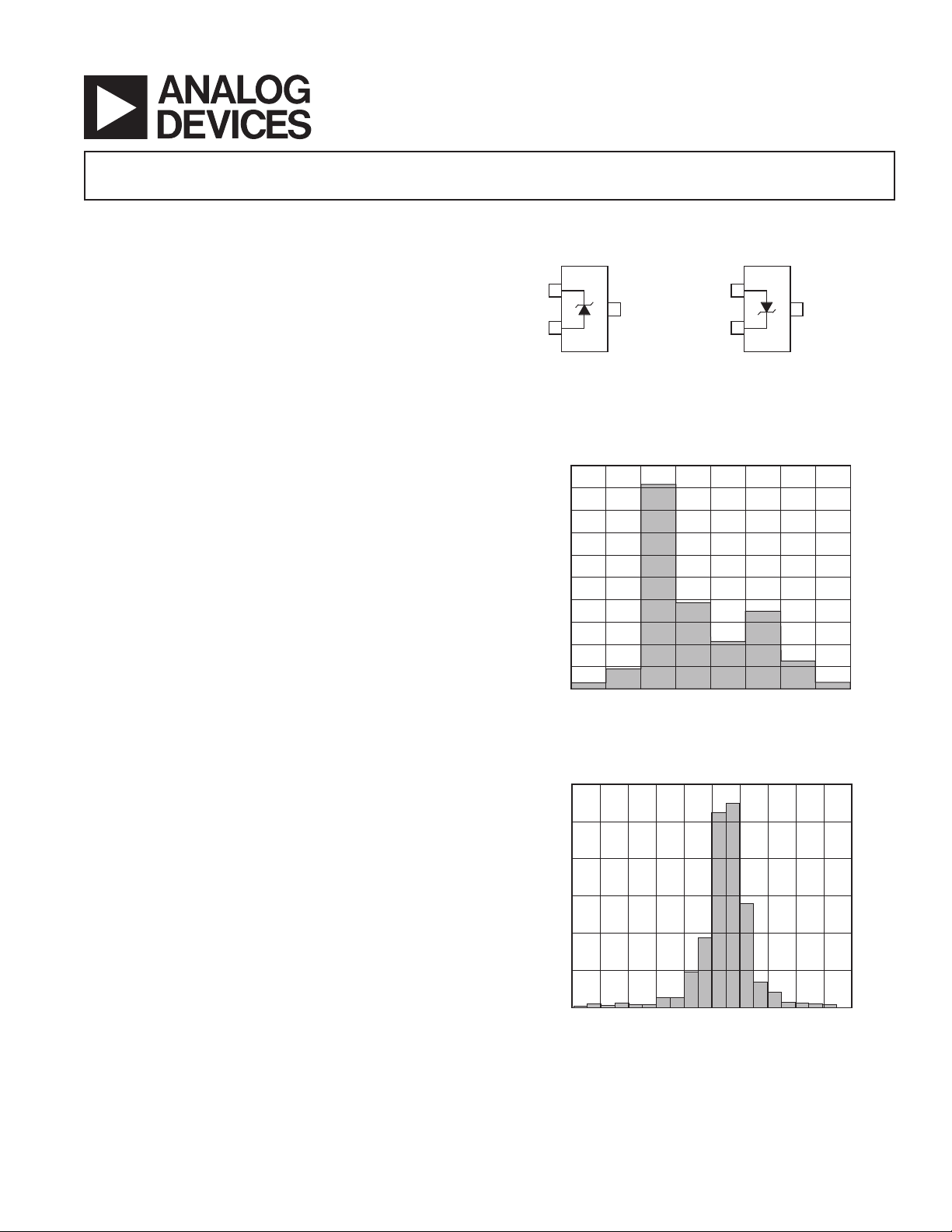
PIN CONFIGURATIONS
SOT-23 Package SC70 Package
1
V+
3
NC (OR V–)
2
V–
TOP
VIEW
NC = NO CONNECT
50
45
40
35
30
25
QUANTITY
20
15
10
5
0
–40 40
–30 –20 –10 0 10 20 30
TEMPERATURE DRIFT (ppm/ ⴗC)
1
V–
2
V+
TOP
VIEW
NC = NO CONNECT
3
NC (OR V–)
Figure 1. Reverse Voltage Temperature Drift Distribution
TARGET APPLICATIONS
1. Portable, Battery-Powered Equipment:
Cellular Phones, Notebook Computers, PDAs, GPSes, and
DMMs
2. Computer Workstations:
Suitable for use with a wide range of video RAMDACs
3. Smart Industrial Transmitters
4. PCMCIA Cards
5. Automotive
6. 3 V/5 V, 8-Bit to 12-Bit Data Converters
*Protected by U.S. Patent No. 5,969,657; other patents pending.
REV. B
Information furnished by Analog Devices is believed to be accurate and
reliable. However, no responsibility is assumed by Analog Devices for its
use, nor for any infringements of patents or other rights of third parties that
may result from its use. No license is granted by implication or otherwise
under any patent or patent rights of Analog Devices. Trademarks and
registered trademarks are the property of their respective owners.
Figure 2. Reverse Voltage Error Distribution
One Technology Way, P.O. Box 9106, Norwood, MA 02062-9106, U.S.A.
Tel: 781/329-4700 www.analog.com
Fax: 781/326-8703 © 2004 Analog Devices, Inc. All rights reserved.

AD1580–SPECIFICATIONS
(@ TA = 25ⴗC, IIN = 100 A, unless otherwise noted.)
AD1580A AD1580B
Model Min Typ Max Min Typ Max Unit
REVERSE VOLTAGE OUTPUT (SOT-23) 1.215 1.225 1.235 1.224 1.225 1.226 V
REVERSE VOLTAGE OUTPUT (SC70) 1.2225 1.225 1.2275 V
REVERSE VOLTAGE TEMPERATURE DRIFT
–40
°C to +85°C 100 50 ppm/°C
MINIMUM OPERATING CURRENT, T
MIN
to T
MAX
50 50 µA
REVERSE VOLTAGE CHANGE WITH REVERSE
CURRENT
50 µA < IIN < 10 mA, T
50 µA < IIN < 1 mA, T
DYNAMIC OUTPUT IMPEDANCE
MIN
MIN
to T
to T
MAX
MAX
(∆VR/∆IR)
2.5 6 2.5 6 mV
0.5 0.5 mV
IIN = 1 mA ⫾100 µA (f = 120 Hz) 0.4 1 0.4 0.5 Ω
OUTPUT NOISE
RMS Noise Voltage: 10 Hz to 10 kHz 20 20 µV
rms
Low Frequency Noise Voltage: 0.1 Hz to 10 Hz 5 5µV p-p
TURN-ON SETTLING TIME TO 0.1%
OUTPUT VOLTAGE HYSTERESIS
1
2
55µs
80 80 µV
TEMPERATURE RANGE
Specified Performance, T
Operating Range
NOTES
1
Measured with no load capacitor.
2
Output hysteresis is defined as the change in the +25°C output voltage after a temperature excursion to +85 °C and then to –40°C.
3
The operating temperature range is defined as the temperature extremes at which the device will continue to function. Parts may deviate from their specified performance.
Specifications subject to change without notice.
3
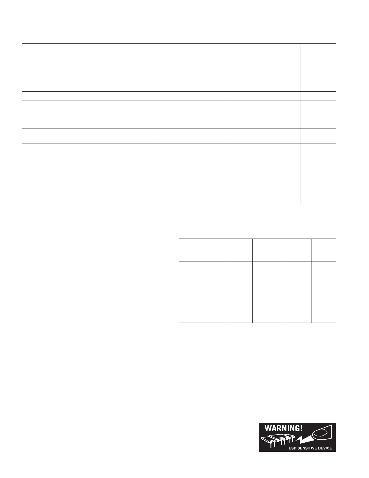
ABSOLUTE MAXIMUM RATINGS
MIN
to T
MAX
1
Reverse Current . . . . . . . . . . . . . . . . . . . . . . . . . . . . . . . 25 mA
Forward Current . . . . . . . . . . . . . . . . . . . . . . . . . . . . . . 20 mA
Internal Power Dissipation
2
SOT-23 (RT) . . . . . . . . . . . . . . . . . . . . . . . . . . . . . . . 0.3 W
Storage Temperature Range . . . . . . . . . . . . –65°C to +150°C
Operating Temperature Range
AD1580/RT . . . . . . . . . . . . . . . . . . . . . . . –55°C to +125°C
Lead Temperature, Soldering
Vapor Phase (60 sec) . . . . . . . . . . . . . . . . . . . . . . . . +215°C
Infrared (15 sec) . . . . . . . . . . . . . . . . . . . . . . . . . . . +220°C
ESD Susceptibility
3
Human Body Model . . . . . . . . . . . . . . . . . . . . . . . . . . 4 kV
Machine Model . . . . . . . . . . . . . . . . . . . . . . . . . . . . . 400 V
NOTES
1
Stresses above those listed under “Absolute Maximum Ratings” may cause
permanent damage to the device. This is a stress rating only and functional
operation of the device at these or any other conditions above those indicated in the
operational section of this specification is not implied. Exposure to absolute
maximum rating conditions for extended periods may affect device reliability.
2
Specification is for device in free air at 25°C: SOT-23 package: θJA = 300°C/W.
3
The human body model is a 100 pF capacitor discharged through 1.5 kΩ. For the
machine model, a 200 pF capacitor is discharged directly into the device.
–40 +85 –40 +85
–55 +125 –55 +125
ORDERING GUIDE
Initial
Output Temperature Package
Model Error Coefficient Option Branding
1
AD1580ART-R2
AD1580ART-REEL
AD1580ART-REEL7
AD1580ARTZ-REEL7
AD1580BRT-R2
AD1580BRT-REEL 1 mV 50 ppm/°C RT-3 0Bxx
AD1580BRT-REEL7
AD1580BRTZ-REEL7
10 mV 100 ppm/°C RT-3 0Axx
2
10 mV 100 ppm/°C RT-3 0Axx
3
10 mV 100 ppm/°C RT-3 0Axx
4
10 mV 100 ppm/°C RT-3 0Axx
1
1 mV 50 ppm/°C RT-3 0Bxx
3
1 mV 50 ppm/°C RT-3 0Bxx
4
1 mV 50 ppm/°C RT-3 0Bxx
AD1580BKSZ-REEL42.5 mV 50 ppm/°CKS-3K0B
NOTES
1
R2 is 250 piece reel.
2
Provided on a 13-inch reel containing 10,000 pieces.
3
Provided on a 7-inch reel containing 3,000 pieces.
4
Z = Pb-free part.
PACKAGE BRANDING INFORMATION
In the SOT-23 package (RT), four marking fields identify the
device generic, grade, and date of processing. The first field is the
product identifier. A 0 identifies the generic as the AD1580. The
°C
°C
second field indicates the device grade: A or B. In the third field
a numeral or letter indicates a calendar year: 5 for 1995, A for
2001. In the fourth field, letters A through Z represent a twoweek window within the calendar year, starting with A for the
first two weeks of January.
CAUTION
ESD (electrostatic discharge) sensitive device. Electrostatic charges as high as 4000 V readily
accumulate on the human body and test equipment and can discharge without detection. Although the
AD1580 features proprietary ESD protection circuitry, permanent damage may occur on devices
subjected to high energy electrostatic discharges. Therefore, proper ESD precautions are recommended
to avoid performance degradation or loss of functionality.
REV. B–2–

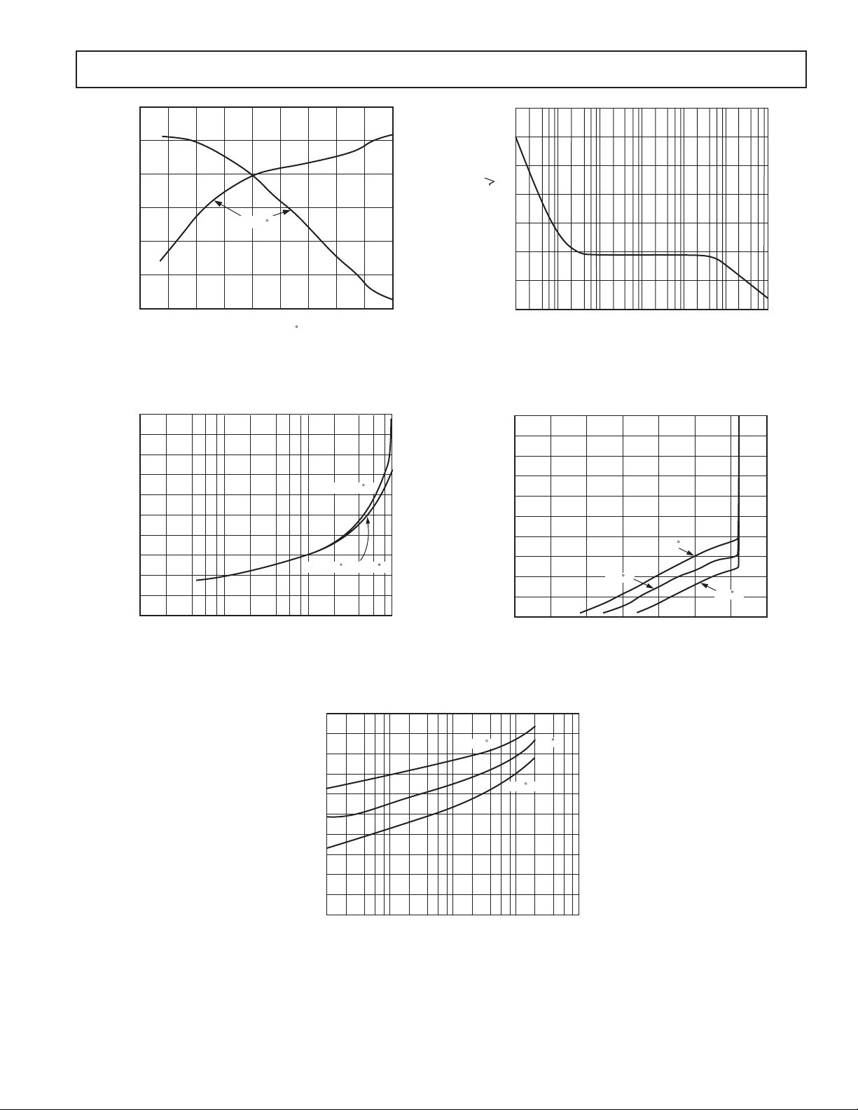
1000
Typical Performance Characteristics–AD1580
500
0
–500
~
20ppm/ C
–1000
–1500
REVERSE VOLTAGE CHANGE (ppm)
–2000
–55
–35 –15 5 25 65 85 125105
TEMPERATURE ( C)
45
TPC 1. Output Drift for Different Temperature
Characteristics
4
3
2
1
0
REVERSE VOLTAGE CHANGE (mV)
–1
0.1 1010.01
REVERSE CURRENT (mA)
TA = 125 C
TA = –40 C TO +85 C
600
400
200
NOISE VOLTAGE (nV/ Hz)
1.0 10 100 1k 10k 100k 1M
FREQUENCY (Hz)
TPC 3. Noise Spectral Density
100
80
60
40
REVERSE CURRENT (A)
20
0
0 1.40.2 0.4 0.6 0.8 1.0 1.2
+25 C
REVERSE VOLTAGE (V)
+85 C
–40 C
TPC 2. Output Voltage Error vs. Reverse Current
1.0
0.8
0.6
0.4
FORWARD VOLTAGE (V)
0.2
0
0.01 100
0.1 1 10
TPC 5. Forward Voltage vs. Forward Current
–40 C
FORWARD CURRENT (mA)
TPC 4. Reverse Current vs. Reverse Voltage
+25 C
+85 C
REV. B
–3–
 Loading...