

1 MSPS 16-/14-Bit
Analog I/O Port
AD15700
FEATURES
16-Bit A/D Converter
1 MSPS
S/(N + D): 90 dB Typ @ 250 kHz
No Pipeline Delay
14-Bit D/A Converter
Settling Time: 1 s
S/N: 92 dB Typ
2 80 MHz Amplifiers
30 V/s Slew Rate
Rail-to-Rail Input and Output
Output Current 15 mA
2 Gain Setting Center Tapped Resistors
Resistor Ratio Tracking: 2 ppm/C
Unipolar Operation
®
/QSPI™/MICROWIRE™/DSP Compatible
SPI
132 mW Typical Power Dissipation
APPLICATIONS
Optical MEMS Mirror Control
Industrial Process Control
Data Acquisition
Instrumentation
Communication
GENERAL DESCRIPTION
The AD15700 is a precision component to interface analog input
and output channels to a digital processor. It is ideal for arealimited applications that require maximum circuit density. The
AD15700 contains the functionality of a 16-bit,
redistribution SAR analog-to-digital converter that
a 5 V power supply. The high speed 16-bit sampling
porates a resistor input scaler that allows various input
internal conversion clock, error correction circuits,
and parallel system interface ports. The AD15700 also
1 MSPS charge
operates from
ADC incor-
ranges, an
and both serial
contains a
14-bit, serial input, voltage output DAC that operates from a 5 V
supply and has a
voltage feedback amplifiers with rail-to-rail input and
characteristics featuring 80 MHz of small signal bandwidth
settling time of 1 ms. Two single- or
split-supply
output
and
10 mV/∞C offset drift provide ADC and DAC buffering capability.
The center tapped 3 kW resistors are precision resistor
networks
with 2 ppm/∞C ratio tracking that provide low gain drift when
used for scaling.
The ADC, DAC, and amp functions are electrically isolated from
each other to provide maximum design flexibility. Input and
output signal conditioning circuits for the converters can be easily
configured with short interconnects under the device at the board
level. The AD15700 is available in a 10 mm CSPBGA package.
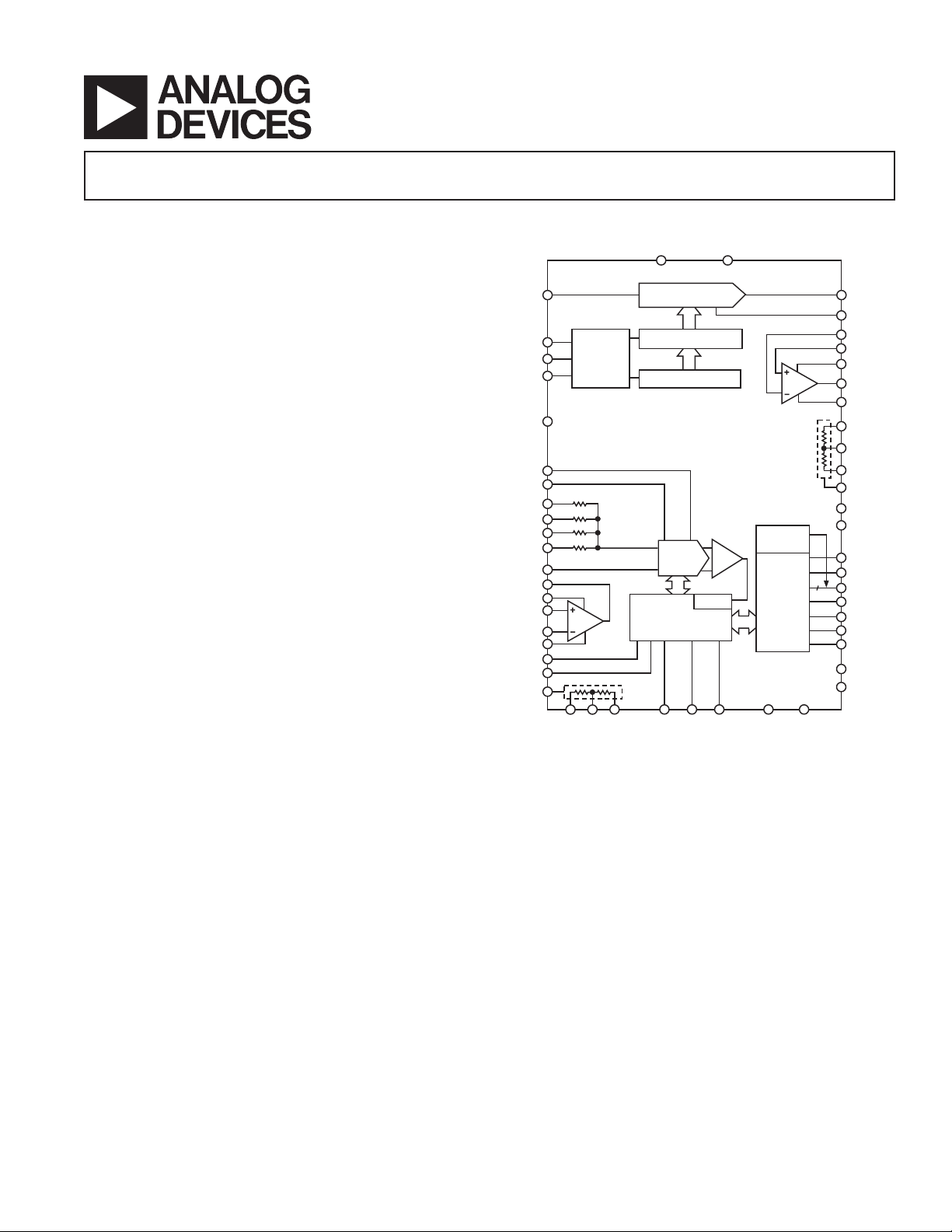
FUNCTIONAL BLOCK DIAGRAM
VDD_DAC DGND_DAC
VREF
CS_DAC
DIN
SCLK
COMMON
REF
REFGND
IND(4R)
INC(4R)
INB(2R)
INA(R)
INGND
VOU T2
+VS2
+IN2
–IN2
–VS2
RESET
RPAD2
CONTROL
LOGIC
4R
4R
2R
R
PD
1.5k
1.5k
RC2
RB2
RA2
14-BIT DAC
14-BIT DATA LATCH
SERIAL INPUT REGISTER
AD15700
SWITCHED
CAP DAC
SAR ADC
CONTROL LOGIC AND
CALIBRATION CIRCUITRY
CLOCK
CNVST
WARP IMPULSE
SERIAL
PORT
PARALLEL
INTERFACE
DVDD
1.5k
1.5k
DGND
ADC
VOU T_DAC
AGND_DAC
–IN1
+IN1
+VS1
VOU T1
–VS1
RA1
RB1
RC1
RPAD1
OVD D
OGND
SER/PAR
BUSY
16
D[15:0]
CS_ADC
RD
OB/2C
BYTESWAP
AVD D
AGND_ADC
PRODUCT HIGHLIGHTS
1. Fast Throughput ADC.
The AD15700 incorporates a high speed, 1 MSPS, 16-bit
SAR ADC.
2. Superior ADC INL.
The 16-bit ADC has a maximum integral nonlineariy of
2.5 LSB with no missing codes.
3. Two Precision Resistor Networks with 2 ppm/∞C Ratio
Tracking for Gain Setting.
4. Low Power Consumption.
Typically 132 mW at maximum performance levels.
5. Industrial Temperature Range: –40∞C to +85∞C.
REV. A
Information furnished by Analog Devices is believed to be accurate and
reliable. However, no responsibility is assumed by Analog Devices for its
use, nor for any infringements of patents or other rights of third parties that
may result from its use. No license is granted by implication or otherwise
under any patent or patent rights of Analog Devices. Trademarks and
registered trademarks are the property of their respective companies.
One Technology Way, P.O. Box 9106, Norwood, MA 02062-9106, U.S.A.
Tel: 781/329-4700 www.analog.com
Fax: 781/326-8703 © 2003 Analog Devices, Inc. All rights reserved.

AD15700–SPECIFICATIONS
(–40C to +85C, AVDD = DVDD = 5 V, 0VDD = 2.7 V to 5.25 V, unless
16-BIT ADC ELECTRICAL CHARACTERISTICS
Parameter Condition Min Typ Max Unit
RESOLUTION 16 Bits
ANALOG INPUT
Voltage Range VIND – VINGND
Common-Mode Input Voltage VINGND –0.1 +0.5 V
Analog Input CMRR f
Input Impedance See Table I
THROUGHPUT SPEED
Complete Cycle In Warp Mode 1 ms
Throughput Rate In Warp Mode 1 1000 kSPS
Time between Conversions In Warp Mode 1 ms
Complete Cycle In Normal Mode 1.25 ms
Throughput Rate In Normal Mode 0 800 kSPS
Complete Cycle In Impulse Mode 1.5 ms
Throughput Rate In Impulse Mode 0 666 kSPS
DC ACCURACY
Integral Linearity Error –2.5 +2.5 LSB
No Missing Codes 16 Bits
Transition Noise 0.7 LSB
Bipolar Zero Error
Bipolar Full-Scale Error2, T
Unipolar Zero Error
Unipolar Full-Scale Error2, T
2
, T
to T
2
MIN
, T
MIN
MIN
to T
MIN
MAX
to T
MAX
to T
MAX
MAX
Power Supply Sensitivity AVDD = 5 V ± 5% ± 9.5 LSB
AC ACCURACY
Signal-to-Noise fIN = 20 kHz 89 90 dB
Spurious-Free Dynamic Range f
Total Harmonic Distortion f
Signal-to-(Noise + Distortion) f
–3 dB Input Bandwidth 9.6 MHz
SAMPLING DYNAMICS
Aperture Delay 2ns
Aperture Jitter 5 ps rms
Transient Response Full-Scale Step 250 ns
REFERENCE
External Reference Voltage Range 2.3 2.5 3.0 V
External Reference Current Drain 1 MSPS Throughput 200 mA
DIGITAL INPUTS
Logic Levels
V
IL
V
IH
I
IL
I
IH
= 100 kHz 74 dB
IN
± 5 V Range, Normal or –45 +45 LSB
Impulse Modes
Other Range or Mode ± 0.1% % of FSR
fIN = 250 kHz 90 dB
= 250 kHz 100 dB
IN
= 20 kHz –100 –96 dB
IN
= 250 kHz –100 dB
f
IN
= 20 kHz 88.5 90 dB
IN
= 250 kHz, –60 dB Input 30 dB
f
IN
otherwise noted.)
± 4 REF, 0 V to 4 REF, ± 2 REF (See Table I)
–0.38 +0.38 % of FSR
–0.18 +0.18 % of FSR
–0.76 +0.76 % of FSR
–0.3 +0.8 V
+2.0
–1 +1 mA
–1 +1 mA
DVDD + 0.3
1
3
V
REV. A–2–
AD15700
Parameter Condition Min Typ Max Unit
DIGITAL OUTPUTS
Data Format Parallel or Serial 16-Bit
Pipeline Delay Conversion Results Available Immediately
after Completed Conversion
I
V
OL
V
OH
POWER SUPPLIES
Specified Performance
AVDD 4.75 5 5.25 V
DVDD 4.75 5 5.25 V
OVDD 2.7 5.25 V
Operating Current
AVDD 15 mA
5
DVDD
5
OVDD
Power Dissipation
In Power-Down Mode
4
5, 6
8
TEMPERATURE RANGE
Specified Performance T
NOTES
1
LSB means Least Significant Bit. With the ± 5 V input range, one LSB is 152.588 mV.
2
These specifications do not include the error contribution from the external reference.
3
All specifications in dB are referred to a full-scale input FS. Tested with an input signal at 0.5 dB below full scale, unless otherwise specified.
4
In Warp Mode.
5
Tested in Parallel Reading Mode.
6
Tested with the 0 V to 5 V range and VIN – VINGND = 0 V.
7
In Impulse Mode.
8
With OVDD below DVDD + 0.3 V and all digital inputs forced to OVDD or OGND, respectively.
Specifications subject to change without notice.
= 1.6 mA 0.4 V
SINK
I
= –570 mA OVDD – 0.6 V
SOURCE
7.2 mA
37 mA
84 95 mW
15 mW
112 125 mW
666 kSPS Throughput
100 SPS Throughput
1 MSPS Throughput
7
4
7
1mW
MIN
to T
MAX
–40 +85 ∞C
Table I. Analog Input Configuration
Input Voltage Range IND(4R) INC(4R) INB(2R) INA(R) Input Impedance
± 4 REF V
± 2 REF V
± REF V
0 V to 4 REF V
0 V to 2 REF V
0 V to REF V
NOTES
1
Typical analog input impedance.
2
For this range, the input is high impedance.
IN
IN
IN
IN
IN
IN
INGND INGND REF 1.63 kW
V
IN
V
IN
V
IN
V
IN
V
IN
INGND REF 948 W
V
IN
REF 711 W
INGND INGND 948 W
V
IN
V
IN
INGND 711 W
V
IN
Note 2
1
REV. A
–3–

AD15700
16-BIT ADC TIMING CHARACTERISTICS
(–40C to +85C, AVDD = DVDD = 5 V, 0VDD = 2.7 V to 5.25 V, unless otherwise noted.)
Parameter Symbol Min Typ Max Unit
Refer to Figures 14 and 15
Convert Pulsewidth t
Time between Conversions
1
t
2
5ns
1/1.25/1.5 Note 1 ms
(Warp Mode/Normal Mode/Impulse Mode)
CNVST LOW to BUSY HIGH Delay t
BUSY HIGH All Modes Except in Master Serial Read after t
3
4
30 ns
0.75/1/1.25
ms
Convert Mode (Warp Mode/Normal Mode/Impulse Mode)
Aperture Delay t
End of Conversion to BUSY LOW Delay t
Conversion Time (Warp Mode/Normal Mode/Impulse Mode) t
Acquisition Time t
RESET Pulsewidth t
5
6
7
8
9
10 ns
1 ms
10 ns
2ns
0.75/1/1.25
ms
Refer to Figures 16, 17, and 18 (Parallel Interface Modes)
CNVST LOW to DATA Valid Delay t
10
0.75/1/1.25
ms
(Warp Mode/Normal Mode/Impulse Mode)
DATA Valid to BUSY LOW Delay t
Bus Access Request to DATA Valid t
Bus Relinquish Time t
Refer to Figures 20 and 21 (Master Serial Interface Modes)
2
CS_ADC LOW to SYNC Valid Delay t
CS_ADC LOW to Internal SCLK Valid Delay t
CS_ADC LOW to SDOUT Delay t
CNVST LOW to SYNC Delay (Read During Convert) t
(Warp Mode/Normal Mode/Impulse Mode)
SYNC Asserted to SCLK First Edge Delay
Internal SCLK Period
Internal SCLK HIGH
Internal SCLK LOW
SDOUT Valid Setup Time
SDOUT Valid Hold Time
SCLK Last Edge to SYNC Delay
3
3
3
3
3
3
3
CS_ADC HIGH to SYNC HI-Z t
CS_ADC HIGH to Internal SCLK HI-Z t
CS_ADC HIGH to SDOUT HI-Z t
BUSY HIGH in Master Serial Read after Convert
3
CNVST LOW to SYNC Asserted Delay t
11
12
13
14
15
16
17
t
18
t
19
t
20
t
21
t
22
t
23
t
24
25
26
27
t
28
29
20 ns
40 ns
515ns
10 ns
10 ns
10 ns
25/275/525 ns
4ns
25 40 ns
15 ns
9ns
4.5 ns
2ns
3ns
10 ns
10 ns
10 ns
See Table II ms
0.75/1/1.25 ms
Master Serial Read after Convert
SYNC Deasserted to BUSY LOW Delay t
30
25 ns
Refer to Figures 22 and 24 (Slave Serial Interface Modes)
External SCLK Setup Time t
External SCLK Active Edge to SDOUT Delay t
SDIN Setup Time t
SDIN Hold Time t
External SCLK Period t
External SCLK HIGH t
External SCLK LOW t
NOTES
1
In Warp Mode only, the maximum time between conversions is 1 ms; otherwise, there is no required maximum time.
2
In Serial Interface Modes, the SYNC, SCLK, and SDOUT timings are defined with a maximum load CL of 10 pF; otherwise, the load is 60 pF maximum.
3
In serial master Read during Convert Mode. See Table II.
Specifications subject to change without notice.
31
32
33
34
35
36
37
5ns
316ns
5ns
5ns
25 ns
10 ns
10 ns
REV. A–4–
AD15700
Table II. Serial Clock Timings in Master Read after Convert
DIVSCLK[1] 0011
DIVSCLK[0]
SYNC to SCLK First Edge Delay Minimum t
Internal SCLK Period Minimum t
Internal SCLK Period Maximum t
Internal SCLK HIGH Minimum t
Internal SCLK LOW Minimum t
SDOUT Valid Setup Time Minimum t
SDOUT Valid Hold Time Minimum t
SCLK Last Edge to SYNC Delay Minimum t
BUSY HIGH Width Maximum (Warp) t
BUSY HIGH Width Maximum (Normal) t
BUSY HIGH Width Maximum (Impulse) t
Symbol
18
19
19
20
21
22
23
24
28
28
28
0101Unit
4202020ns
25 50 100 200 ns
40 70 140 280 ns
15 25 50 100 ns
9244999ns
4.5 22 22 22 ns
243089ns
360140 300 ns
1.5 2 3 5.25 ms
1.75 2.25 3.25 5.5 ms
2 2.5 3.5 5.75 ms
1.6mA
TO OUTPUT
PIN
IN SERIAL INTERFACE MODES, THE SYNC, SCLK, AND
SDOUT TIMINGS ARE DEFINED WITH A MAXIMUM LOAD
C
OF 10pF; OTHERWISE THE LOAD IS 60pF MAXIMUM.
L
C
L
60pF
500mA
I
OL
1.4V
I
OH
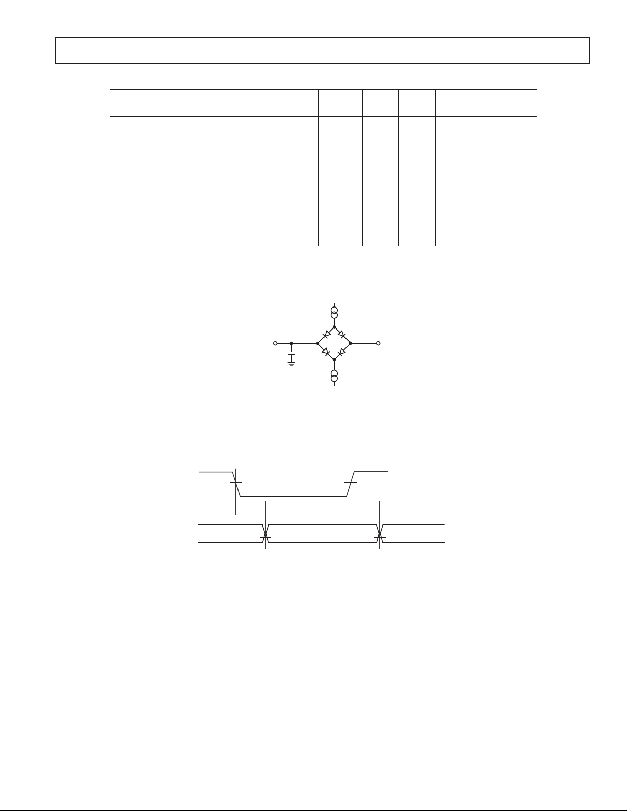
Figure 1. Load Circuit for Digital Interface Timing, SDOUT, SYNC, SCLK Outputs, CL = 10 pF
0.8V
t
DELAY
2V
0.8V
2V
t
DELAY
2V
0.8V
Figure 2. Voltage Reference Levels for Timing
REV. A
–5–

AD15700
14-BIT DAC ELECTRICAL CHARACTERISTICS
(TA = –40C to +85C, VDD_DAC = 5 V, V
= 2.5 V, unless otherwise noted.)
REF
Parameter Condition Min Typ Max Unit
STATIC PERFORMANCE
Resolution 1 LSB = V
when V
/214 = 153 mV
REF
= 2.5 V 14 Bits
REF
Relative Accuracy, INL ± 0.15 ± 1.0 LSB
Differential Nonlinearity Guaranteed Monotonic ± 0.15 ± 0.8 LSB
Gain Error –1.75 –0.3 0 LSB
Gain Error Temperature Coefficient
± 0.1 ppm/∞C
Zero Code Error 0 0.1 0.5 LSB
Zero Code Temperature Coefficient
± 0.05 ppm/∞C
OUTPUT CHARACTERISTICS
Output Voltage Range 0 V
Output Voltage Settling Time
To 1/2 LSB of FS, CL = 10 pF
1 ms
–1 LSB V
REF
Digital-to-Analog Glitch Impulse 1 LSB Change around the
Major Carry 10 nV–s
Digital Feedthrough All 1s Loaded to DAC,
= 2.5 V 0.05 nV–s
V
REF
DAC Output Impedance Tolerance Typically 20% 6.25 kW
Power Supply Rejection Ratio DVDD ± 10% ± 1.0 LSB
DAC REFERENCE INPUT
Reference Input Range 2 V
DD
V
Reference Input Resistance* 9kW
LOGIC INPUTS
Input Current ± 1.0 mA
VINL, Input Low Voltage 0.8 V
VINH, Input High Voltage 2.4 V
Input Capacitance 10 pF
Hysteresis Voltage 0.4 V
REFERENCE
Reference –3 dB Bandwidth All 1s Loaded 1.3 MHz
Reference Feedthrough All 0s Loaded,
= 1 V p-p at 100 kHz 1 mV p-p
V
REF
Signal-to-Noise Ratio 92 dB
Reference Input Capacitance Code 0000
Code 3FFF
H
H
75 pF
120 pF
POWER REQUIREMENTS
V
DD
I
DD
4.5 5.50 V
0.3 1.1 mA
Power Dissipation 1.5 6.05 mW
*Reference input resistance is code-dependent, minimum at 2555H.
Specifications subject to change without notice.
REV. A–6–
AD15700
(VDD = 5 V, 5%, V
1, 2
14-BIT DAC TIMING CHARACTERISTICS
Parameter Limit at T
f
SCLK
t
1
t
2
t
3
t
4
t
5
t
6
t
7
t
8
t
9
t
10
NOTES
1
Guaranteed by design. Not production tested.
2
Sample tested during initial release and after any redesign or process change that may affect this parameter. All input signals are measured with tr = tf = 5 ns (10% to 90%
of 3 V and timed from a voltage level of 1.6 V).
Specifications subject to change without notice.
25 MHz max SCLK Cycle Frequency
40 ns min SCLK Cycle Time
20 ns min SCLK High Time
20 ns min SCLK Low Time
15 ns min CS_DAC Low to SCLK High Setup
15 ns min CS_DAC High to SCLK High Setup
35 ns min SCLK High to CS_DAC Low Hold Time
20 ns min SCLK High to CS_DAC High Hold Time
15 ns min Data Setup Time
0 ns min Data Hold Time
30 ns min CS_DAC High Time between Active Periods
SCLK
CS_DAC
DIN
MIN
, T
All Versions Unit Description
MAX
t
6
t
4
t
10
t
8
t
9
DB13
TA = T
t
2
to T
MIN
MAX
t
1
t
3
DB0
= 2.5 V, AGND = DGND = 0 V. All Specifications
REF
, unless otherwise noted).
t
5
t
7
REV. A
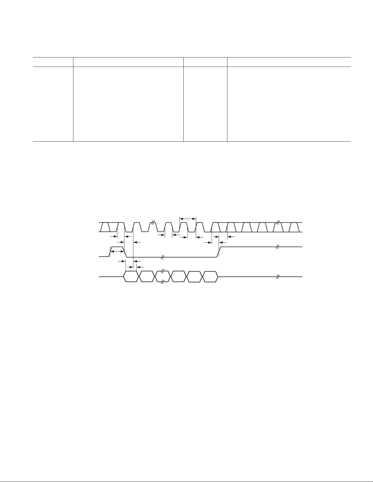
Figure 3. Timing Diagram
–7–

AD15700
[5 V Supply (TA = 25C, VS = 5 V, RL = 1 k to 2.5 V, RF = 2.5 k,
AMPLIFIER ELECTRICAL CHARACTERISTICS
Parameter Condition Min Typ Max Unit
DYNAMIC PERFORMANCE
–3 dB Small Signal Bandwidth G = +1, V
Slew Rate G = –1, VO = 2 V Step 27 32 V/ms
Settling Time to 0.1% G = –1, V
DISTORTION/NOISE PERFORMANCE
Total Harmonic Distortion fC = 1 MHz, VO = 2 V p-p, G = +2 –62 dBc
= 100 kHz, VO = 2 V p-p, G = +2 –86 dBc
f
C
Input Voltage Noise f = 1 kHz 15
Input Current Noise f = 100 kHz 2.4 pA
f = 1 kHz 5 pA
Differential Gain RL = 1 kW 0.17 %
Differential Phase R
= 1 kW 0.11
L
DC PERFORMANCE
Input Offset Voltage VCM = VCC/2; V
T
MIN
Offset Drift VCM = VCC/2; V
Input Bias Current VCM = VCC/2; V
T
MIN
Input Offset Current 50 350 nA
Open-Loop Gain VCM = VCC/2; V
T
MIN
INPUT CHARACTERISTICS
Common-Mode Input Resistance 40 MW
Differential Input Resistance 280 kW
Input Capacitance 1.6 pF
Input Voltage Range –0.5 to +5.5 V
Input Common-Mode Voltage Range –0.2 to +5.2 V
Common-Mode Rejection Ratio VCM = 0 V to 5 V 56 70 dB
VCM = 0 V to 3.8 V 66 80 dB
Differential/Input Voltage 3.4 V
OUTPUT CHARACTERISTICS
Output Voltage Swing Low RL = 10 kW 0.05 0.02 V
Output Voltage Swing High 4.95 4.98 V
Output Voltage Swing Low RL = 1 kW 0.2 0.1 V
Output Voltage Swing High 4.8 4.9 V
Output Current 15 mA
Short Circuit Current Sourcing 28 mA
Sinking –46 mA
Capacitive Load Drive G = +2 15 pF
POWER SUPPLY
Operating Range 2.7 12 V
Quiescent Current per Amplifier 800 1400 mA
Power Supply Rejection Ratio VS– = 0 V to –1 V or 75 86 dB
VS+ = 5 V to 6 V
OPERATING TEMPERATURE RANGE
Specifications subject to change without notice.
< 0.4 V p-p 54 80 MHz
O
= 2 V Step, CL = 10 pF 125 ns
O
to T
to T
to T
OUT
MAX
OUT
OUT
MAX
OUT
MAX
unless otherwise noted.)]
nV/÷Hz
/÷Hz
/÷Hz
Degrees
= 2.5 V ± 1 ± 6mV
± 6 ± 10 mV
= 2.5 V 5 mV/∞C
= 2.5 V 0.45 1.2 mA
2.0 mA
= 1.5 V to 3.5 V 76 82 dB
74 dB
–40 +85 ∞C
REV. A–8–

AD15700
[5 V Supply (TA = 25C, VS = 5 V, RL = 1 k to 0 V, RF = 2.5 k,
AMPLIFIER ELECTRICAL CHARACTERISTICS
Parameter Condition Min Typ Max Unit
DYNAMIC PERFORMANCE
–3 dB Small Signal Bandwidth G = +1, V
Slew Rate G = –1, V
Settling Time to 0.1% G = –1, V
DISTORTION/NOISE PERFORMANCE
Total Harmonic Distortion fC = 1 MHz, VO = 2 V p-p, G = +2 –62 dBc
f
= 100 kHz, VO = 2 V p-p, G = +2 –86 dBc
C
Input Voltage Noise f = 1 kHz 15 nV
Input Current Noise f = 100 kHz 2.4 pA
f = 1 kHz 5 pA
Differential Gain RL = 1 kW 0.15 %
Differential Phase R
= 1 kW 0.15
L
DC PERFORMANCE
Input Offset Voltage VCM = 0 V; V
T
MIN
Offset Drift VCM = 0 V; V
Input Bias Current VCM = 0 V; V
T
MIN
Input Offset Current 50 350 nA
Open-Loop Gain VCM = 0 V; V
T
MIN
INPUT CHARACTERISTICS
Common-Mode Input Resistance 40 MW
Differential Input Resistance 280 kW
Input Capacitance 1.6 pF
Input Voltage Range –5.5 to +5.5 V
Input Common-Mode Voltage Range
Common-Mode Rejection Ratio VCM = –5 V to +5 V 60 80 dB
VCM = –5 V to +3.5 V 66 90 dB
Differential/Input Voltage 3.4 V
OUTPUT CHARACTERISTICS
Output Voltage Swing Low RL = 10 kW –4.94 –4.98 V
Output Voltage Swing High +4.94 +4.98 V
Output Voltage Swing Low RL = 1 kW –4.7 –4.85 V
Output Voltage Swing High +4.7 +4.75 V
Output Current 15 mA
Short Circuit Current Sourcing +35 mA
Sinking –50 mA
Capacitive Load Drive G = +2 15 pF
POWER SUPPLY
Operating Range ± 1.35 ± 6 V
Quiescent Current per Amplifier 900 1600 mA
Power Supply Rejection Ratio VS– = –5 V to –6 V or 76 86 dB
VS+ = +5 V to +6 V
OPERATING TEMPERATURE RANGE
Specifications subject to change without notice.
< 0.4 V p-p 54 80 MHz
O
= 2 V Step 30 35 V/ms
O
= 2 V Step, CL = 10 pF 125 ns
O
to T
to T
to T
OUT
MAX
OUT
OUT
MAX
OUT
MAX
unless otherwise noted.)]
/÷Hz
/÷Hz
/÷Hz
Degrees
= 0 V ± 1 ± 6 mV
± 6 ± 10 mV
= 0 V 5 mV/∞C
= 0 V 0.45 1.2 mA
2.0 mA
= ± 2 V 76 80 dB
74 dB
–5.2 to +5.2 V
–40 +85 ∞C
REV. A
–9–
AD15700
RESISTOR DIVIDER ELECTRICAL CHARACTERISTICS
(@ TA = 25C, unless otherwise noted.)
Parameter Condition Min Typ Max Unit
Resistance 2.97 3.00 3.03 kW
Temperature Coefficient of Resistance 50 ppm/∞C
Resistance Ratio of Two Halves 0.99 1.0 1.01
Resistance Ratio Tracking 2 ppm/∞C
Power Dissipation TA = 70∞C 250* mW
At higher temperatures, linearly derates to 0 mW at 175∞ C.
*
Specifications subject to change without notice.
ABSOLUTE MAXIMUM RATINGS*
Analog Inputs
IND, INC, INB . . . . . . . . . . . . . . . . . . . . . . –11 V to +30 V
INA, REF, INGND, REFGND, AGND . . .
–0.3 V to AVDD + 0.3 V
ADC Ground Voltage Differences
AGND_ADC, DGND_ADC, OGND . . . . . . . . . . . . ± 0.3 V
ADC Supply Voltages
AVDD, DVDD, OVDD . . . . . . . . . . . . . . . . . . . . . . . . . . 7 V
AVDD to DVDD, AVDD to OVDD . . . . . . . . . . . . . . ± 7 V
DVDD to OVDD . . . . . . . . . . . . . . . . . . . . . . . . . . . . . ± 7 V
ADC Digital Inputs . . . . . . . . . . . . . –0.3 V to DVDD + 0.3 V
VDD_DAC to AGND_DAC . . . . . . . . . . . . . . . –0.3 V to +6 V
DAC Digital Input Voltage to
DGND_DAC . . . . . . . . . . . . . . . . –0.3 V to DVDD + 0.3 V
VOUT_DAC to AGND_DAC . . . . –0.3 V to DVDD + 0.3 V
AGND_DAC to DGND_DAC . . . . . . . . . . . –0.3 V to +0.3 V
DAC Input Current to Any DAC Pin Except Supplies . . ± 10 mA
Amplifier Supply Voltage (VS1, VS2) . . . . . . . . . . . . . . 12.6 V
Amplifier Input Voltage (Common Mode) . . . . . . ± V
± 0.5 V
S
Amplifier Differential Input Voltage . . . . . . . . . . . . . . . ± 3.4 V
Amplifier Output Short Circuit
Duration . . . . . . . . . . . . . . Observe Power Derating Curves
Resistor Instantaneous Voltage Drop . . . . . . . . . . . . . . . ± 50 V
Internal Power Dissipation . . . . . . . . . . . . . (T
Thermal Resistance
JA
Max – TA)/
J
10 mm CSPBGA . . . . . . . . . . . . . . . . . . . . . . . . . . . 42∞C/W
Maximum Junction Temperature (T
Max) . . . . . . . . . . 150∞C
J
Operating Temperature Range . . . . . . . . . . . . –40∞C to +85∞C
Storage Temperature Range . . . . . . . . . . . . . –65∞C to +150∞C
Lead Temperature . . . . . . . . . . . . . . . . . . . . . . . 225∞C, 15 sec
*Stresses above those listed under Absolute Maximum Ratings may cause perma-
nent damage to the device. This is a stress rating only and functional operation of
the device at these or any other conditions above those indicated in the operational
sections of this specification is not implied. Exposure to absolute maximum rating
conditions for extended periods may affect device reliability.
JA
ORDERING GUIDE
Model Temperature Range Package Option
AD15700BCA –40∞C to +85∞C 144-Lead CSPBGA
AD15700/PCB 25∞C Evaluation Board
ADDS-2191-EZLITE
™
25∞C Evaluation Kit*
ADDS-21535-EZLITE
ADDS-21160M-EZLITE
ADDS-21161N-EZLITE
*One of the DSP Evaluation Kits is required for operation of the AD15700/PCB Evaluation Board.
CAUTION
ESD (electrostatic discharge) sensitive device. Electrostatic charges as high as 4000 V readily
accumulate on the human body and test equipment and can discharge without detection. Although the
AD15700 features proprietary ESD protection circuitry, permanent damage may occur on devices
subjected to high energy electrostatic discharges. Therefore, proper ESD precautions are recommended
to avoid performance degradation or loss of functionality.
REV. A–10–

AD15700
ADC PIN FUNCTION DESCRIPTIONS (See Pinout, page 42)
Pin No. Mnemonic Type Description
H9, J8, AGND_ADC P Analog Power Ground Pin
J9, M12
M6 AVDD P Input Analog Power Pin. Nominally 5 V.
L7 BYTESWAP DI Parallel Mode Selection (8-/16-Bit). When LOW, the LSB is output on D[7:0] and the MSB
is output on D[15:8]. When HIGH, the LSB is output on D[15:8] and the MSB is
output on D[7:0].
L8 OB/2C DI Straight Binary/Binary Twos Complement. When OB/2C is HIGH, the digital output
is straight binary; when LOW, the MSB is inverted, resulting in a twos complement
output from its internal shift register.
M7 WARP DI Mode Selection. When HIGH and IMPULSE LOW, this input selects the fastest mode,
the maximum throughput is achievable, and a minimum conversion rate must be applied
in order to guarantee full specified accuracy. When LOW, full accuracy is maintained
independent of the minimum conversion rate.
L9 IMPULSE DI Mode Selection. When HIGH and WARP LOW, this input selects a reduced power mode.
In this mode, the power dissipation is approximately proportional to the sampling rate.
M8 SER/PAR DI Serial/Parallel Selection Input. When LOW, the Parallel Port is selected; when HIGH,
the Serial Interface Mode is selected and some bits of the DATA bus are used as a
serial port.
M9, L10 D[0:1] DO Bit 0 and Bit 1 of the Parallel Port Data Output Bus. When SER/PAR is HIGH, these
outputs are in high impedance.
M10, L11 D[2:3] or DI/O When SER/PAR is HIGH, EXT/INT is LOW and RDC/SDIN is LOW, which is the
DIVSCLK[0:1] serial master read DIVSCLK[0:1] after Convert Mode. These inputs, part of the Serial
Port, are used to slow down, if desired, the internal serial clock that clocks the data output.
In the other serial modes, these inputs are not used.
M11 D[4] or EXT/INT DI/O When SER/PAR is LOW, this output is used as Bit 4 of the Parallel Port Data Output
Bus. When SER/PAR is HIGH, this input, part of the Serial Port, is used as a digital
select input for choosing the internal or an external data clock, called, respectively, Master
and Slave Mode. With EXT/INT tied LOW, the internal clock is selected on SCLK
output. With EXT/INT set to a logic HIGH, output data is synchronized to an external
clock signal connected to the SCLK input and the external clock is gated by CS_ADC.
L12 D[5] or INVSYNC DI/O When SER/PAR is LOW, this output is used as Bit 5 of the Parallel Port Data Output
Bus. When SER/PAR is HIGH, this input, part of the Serial Port, is used to select the
active state of the SYNC signal. When LOW, SYNC is active HIGH. When HIGH,
SYNC is active LOW.
K11 D[6] or INVSCLK DI/O When SER/PAR is LOW, this output is used as Bit 6 of the Parallel Port Data Output
Bus. When SER/PAR is HIGH, this input, part of the Serial Port, is used to invert the
SCLK signal. It is active in both Master and Slave Mode.
K12 D[7] or RDC/SDIN DI/O When SER/PAR is LOW, this output is used as Bit 7 of the Parallel Port Data Output
Bus. When SER/PAR is HIGH, this input, part of the serial port, is used as either an
external data input or a read mode selection input, depending on the state of EXT/INT.
When EXT/INT is HIGH, RDC/SDIN could be used as a data input to daisy-chain
the conversion results from two or more ADCs onto a single SDOUT line. The digital
data level on SDIN is output on DATA with a delay of 16 SCLK periods after the
initiation of the read sequence. When EXT/INT is LOW, RDC/SDIN is used to select
the read mode. When RDC/SDIN is HIGH, the previous data is output on SDOUT
during conversion. When RDC/SDIN is LOW, the data can be output on SDOUT
only when the conversion is complete.
J10 OGND P Input/Output Interface Digital Power Ground
J11 OVDD P Input/Output Interface Digital Power. Nominally at the same supply as the supply of
the host interface (5 V or 3.3 V).
J12 DVDD P Digital Power. Nominally at 5 V.
REV. A
–11–

AD15700
ADC PIN FUNCTION DESCRIPTIONS (continued)
Pin No. Mnemonic Type Description
H10 DGND_ADC P Digital Power Ground
H12 D[8] or SDOUT DO When SER/PAR is LOW, this output is used as Bit 8 of the Parallel Port Data Output
Bus. When SER/PAR is HIGH, this input, part of the serial port, is used as a serial data
output synchronized to SCLK. Conversion results are stored in an on-chip register.
The ADC provides the conversion result, MSB first, from its internal shift register.
The DATA format is determined by the logic level of OB/2C. In Serial Mode, when
EXT/INT is LOW, SDOUT is valid on both edges of SCLK. In Serial Mode, when
EXT/INT is HIGH: If INVSCLK is LOW, SDOUT is updated on SCLK rising edge
and valid on the next falling edge. If INVSCLK is HIGH, SDOUT is updated on
SCLK falling edge and valid on the next rising edge.
H11 D[9] or SCLK DI/O When SER/PAR is LOW, this output is used as Bit 9 of the Parallel Port Data Output
Bus. When SER/PAR is HIGH, this input, part of the Serial Port, is used as a serial
data clock input or output, dependent upon the logic state of the EXT/INT pin. The
active edge where the data SDOUT is updated depends upon the logic state of the
INVSCLK pin.
G12 D[10] or SYNC DO When SER/PAR is LOW, this output is used as Bit 10 of the Parallel Port Data Output
Bus. When SER/PAR is HIGH, this input, part of the Serial Port, is used as a digital
output frame synchronization for use with the internal data clock (EXT/INT = Logic
LOW). When a read sequence is initiated and INVSYNC is LOW, SYNC is driven HIGH
and remains HIGH while SDOUT output is valid. When a read sequence is initiated
and INVSYNC is High, SYNC is driven LOW and remains LOW while SDOUT output
is valid.
G11 D[11] or RDERROR DO When SER/PAR is LOW, this output is used as Bit 11 of the Parallel Port Data Output
Bus. When SER/PAR is HIGH and EXT/INT is HIGH, this output, part of the Serial
Port, is used as an incomplete read error flag. In Slave Mode, when a data read is started
and not complete when the following conversion is complete, the current data is lost
and RDERROR is pulsed high.
F12, F11, D[12:15] DO Bit 12 to Bit 15 of the Parallel Port Data Output Bus. When SER/PAR is HIGH,
E12, E11 these outputs are in high impedance.
G10 BUSY DO Busy Output. Transitions HIGH when a conversion is started, and remains HIGH
until the conversion is complete and the data is latched into the on-chip shift register.
The falling edge of BUSY could be used as a data ready clock signal.
G9 DGND_ADC P Must be Tied to Digital Ground
E10 RD DI Read Data. When CS_ADC and RD are both LOW, the interface parallel or serial
output bus is enabled.
K10 CS_ADC DI Chip Select. When CS_ADC and RD are both LOW, the interface parallel or serial
output bus is enabled. CS_ADC is also used to gate the external serial clock.
D12 RESET DI Reset Input. When set to a logic HIGH, reset the ADC. Current conversion, if any,
is aborted. If not used, this pin could be tied to DGND.
K9 PD DI Power-Down Input. When set to a logic HIGH, power consumption is reduced and
conversions are inhibited after the current one is completed.
E7 CNVST DI Start Conversion. A falling edge on CNVST puts the internal sample/hold into the hold
state and initiates a conversion. In impulse mode (IMPULSE HIGH and WARP LOW),
if CNVST is held low when the acquisition phase (t
sample/hold is put into the hold state and a conversion is immediately started.
H8 AGND_ADC P Must be Tied to Analog Ground
G5 REF AI Reference Input Voltage
H5 REFGND AI Reference Input Analog Ground
J7 INGND P Analog Input Ground
J5, K5, INA, INB, AI Analog Inputs. Refer to Table I for input range configuration.
L5, M5 INC, IND
) is complete, the internal
8
REV. A–12–
AD15700
DAC PIN FUNCTION DESCRIPTIONS
Pin No. Mnemonic Type Description
A6 VOUT_DAC AO Analog Output Voltage from the DAC
A3, C3, C4 AGND_DAC P Ground Reference Point for Analog Circuitry
A2 VREF AI This is the voltage reference input for the DAC. Connect to external reference
ranges from 2 V to VDD.
B1 CS_DAC DI This is an active low logic input signal. The chip select signal is used to frame
the serial data input.
E1 SCLK DI
E2 DIN DI Serial Data Input. This device accepts 14-bit words. Data is clocked into the
E3 DGND_DAC P Digital Ground. Ground reference for digital circuitry.
C6 VDD_DAC P Analog Supply Voltage, 5 V ± 10%
AMPLIFIER PIN FUNCTION DESCRIPTIONS
Pin No. Mnemonic Type Description
C9 (J1) +IN1(2) AI Positive Input Voltage
A9 (G1) –IN1(2) AI Negative Input Voltage
B12 (K4) VOUT1(2) AO Amplifier Output Voltage
A11 (F3) +VS1(2) P Analog Positive Supply Voltage
B10, B11 –VS1(2) P Analog Negative Supply Voltage
(G3, H3)
Clock Input. Data is clocked into the input register on the rising edge of SCLK.
Duty cycle must be between 40% and 60%.
input register on the rising edge of SCLK.
RESISTOR PIN FUNCTION DESCRIPTIONS
Pin No. Mnemonic Type Description
B9 (L4) RA1(2) AI/O Resistor End Terminal
A8 (M4) RB1(2) AI/O Resistor Center Tap
D9 (L1) RC1(2) AI/O Resistor End Terminal
A7 (M3) RPAD1(2) P Resistor Die Pad. Tie to Analog Ground.
COMMON PIN FUNCTION DESCRIPTIONS
Pin No. Mnemonic Type Description
A1, A4, A5, A10, A12, B2–B8, C1, COMMON P Common Floating Net Connecting 69 Pins. Not electrically
C2, C5, C7, C8, C10–C12, D1–D8, connected within the module. Tie at least one of these pins
D10, D11, E4–E6, E8, E9, F1, F2, to Analog Ground.
F4–F10, G2, G4, G6–G8, H1, H2,
H4, H6, H7, J2–J4, J6, K1–K3,
K6–K8, L2, L3, L6, M1, M2
NOTES
AI = Analog Input
AI/O = Bidirectional Analog
AO = Analog Output
DI = Digital Input
DI/O = Bidirectional Digital
DO = Digital Output
P = Power
REV. A
–13–

AD15700
ADC DEFINITION OF SPECIFICATIONS
Integral Nonlinearity Error (INL)
Linearity error refers to the deviation of each individual code
from a line drawn from “negative full scale” through “positive
full scale.” The point used as negative full scale occurs 1/2 LSB
before the first code transition. Positive full scale is defined as a
level 1 1/2 LSB beyond the last code transition. The deviation is
measured from the middle of each code to the true straight line.
Differential Nonlinearity Error (DNL)
In an ideal ADC, code transitions are 1 LSB apart. Differential
nonlinearity is the maximum deviation from this ideal value.
It is often specified in terms of resolution for which no missing
codes are guaranteed.
Full-Scale Error
The last transition (from 011...10 to 011...11 in twos complement coding) should occur for an analog voltage 1 1/2 LSB
below the nominal full scale (2.499886 V for the ± 2.5 V range).
The full-scale error is the deviation of the actual level of the last
transition from the ideal level.
Bipolar Zero Error
The difference between the ideal midscale input voltage (0 V)
and the actual voltage producing the midscale output code.
Unipolar Zero Error
In unipolar mode, the first transition should occur at a level
1/2 LSB above analog ground. The unipolar zero error is the
deviation of the actual transition from that point.
Spurious Free Dynamic Range (SFDR)
The difference, in decibels (dB), between the rms amplitude of
the input signal and the peak spurious signal.
Effective Number of Bits (ENOB)
A measurement of the resolution with a sine wave input. It is
related to S/(N + D) by the following formula:
ENOB S N D
and is expressed in bits.
Total Harmonic Distortion (THD)
The rms sum of the first five harmonic components to the rms
value of a full-scale input signal; expressed in decibels.
Signal-to-Noise Ratio (SNR)
The ratio of the rms value of the actual input signal to the rms
sum of all other spectral components below the Nyquist frequency,
excluding harmonics and dc. The value for SNR is expressed in
decibels.
Signal-to-(Noise + Distortion) Ratio (S/[N + D])
The ratio of the rms value of the actual input signal to the rms
sum of all other spectral components below the Nyquist frequency,
including harmonics but excluding dc. The value for S/(N + D)
is expressed in decibels.
Aperture Delay
A measure of the acquisition performance, measured from the
falling edge of the CNVST input to when the input signal is
held for a conversion.
Transient Response
The time required for the ADC to achieve its rated accuracy
after a full-scale step function is applied to its input.
=+
/–./.176 602
[]
()
()
dB
DAC DEFINITION OF SPECIFICATIONS
Relative Accuracy
For the DAC, relative accuracy or integral nonlinearity (INL)
is a measure of the maximum deviation in LSBs from a straight
line passing through the endpoints of the DAC transfer function.
A typical INL versus code plot can be seen in TPC 16.
Differential Nonlinearity
Differential nonlinearity is the difference between the measured
change and the ideal 1 LSB change between any two adjacent
codes. A specified differential nonlinearity of ± 1 LSB maximum
ensures monotonicity. TPC 19 illustrates a typical DNL versus
code plot.
Gain Error
Gain error is the difference between the actual and ideal analog
output range, expressed as a percent of the full-scale range. It is
the deviation in slope of the DAC transfer characteristic from ideal.
Gain Error Temperature Coefficient
This is a measure of the change in gain error with changes in
temperature. It is expressed in ppm/∞C.
Zero Code Error
Zero code error is a measure of the output error when zero code
is loaded to the DAC register.
Zero Code Temperature Coefficient
This is a measure of the change in zero code error with a change
in temperature. It is expressed in mV/∞C.
Digital-to-Analog Glitch Impulse
Digital-to-analog glitch impulse is the impulse injected into the
analog output when the input code in the DAC register changes
state. It is normally specified as the area of the glitch in nV–s
and is measured when the digital input code is changed by 1 LSB
at the major carry transition. A plot of the glitch impulse is shown
in Figure 28.
Digital Feedthrough
Digital feedthrough is a measure of the impulse injected into the
analog output of the DAC from the digital inputs of the DAC, but
is measured when the DAC output is not updated. CS_DAC is
held high, while the CLK and DIN signals are toggled. It is
specified in nV–s and is measured with a full-scale code change
on the data bus, i.e., from all 0s to all 1s and vice versa. A typical
plot of digital feedthrough is shown in Figure 27.
Power Supply Rejection Ratio
This specification indicates how the output of the DAC is affected
by changes in the power supply voltage. Power supply rejection
ratio is quoted in terms of percent change in output per percent
change in V
by ± 10%.
Reference Feedthrough
This is a measure of the feedthrough from the V
DAC output when the DAC is loaded with all 0s. A 100 kHz,
1Vp-p is applied to V
in mV p-p.
for full-scale output of the DAC. VDD is varied
DD
input to the
REF
. Reference feedthrough is expressed
REF
REV. A–14–

16-BIT D/A CONVERTER
CODE IN HEXADECIMAL
7000
7FFD 7FFE
COUNTS
6000
5000
2000
4000
3000
8000
7FFF 8000 8001 8002 8003 8004 8005 8006 8007
1000
0
1297
1700
7029 7039
986
0025
CODE IN HEXADECIMAL
9000
7FFC 7FFD
COUNTS
8000
7000
4000
6000
5000
10000
7FFE
8001 8002 8003 8004 8005 80068000
3000
0
200001
2000
1000
7FFF 8007
3296
9503
3344
106
132
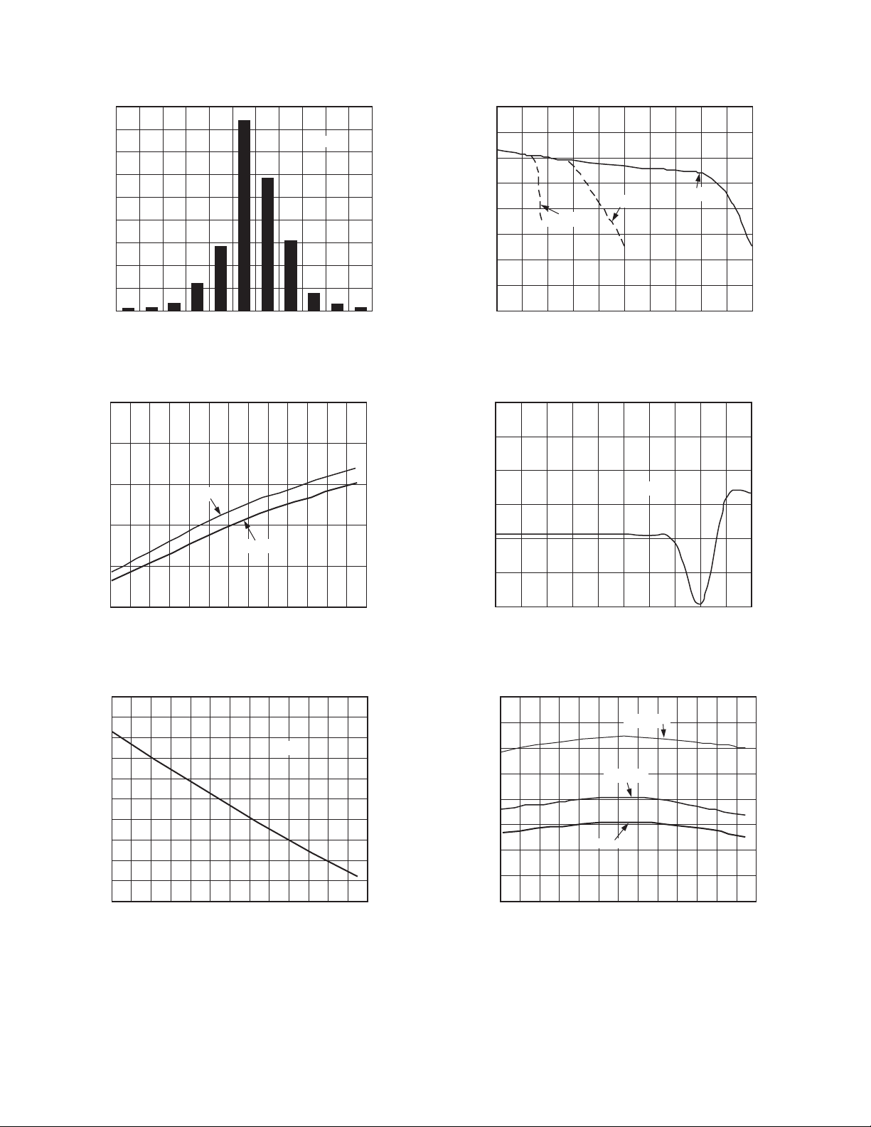
Typical Performance Characteristics–
AD15700
2.5
2.0
1.5
1.0
0.5
0.0
INL – LSB
–0.5
–1.0
–1.5
–2.0
–2.5
0 16384 32768 49152 65536
CODE
TPC 1. Integral Nonlinearity vs. Code
1.75
1.50
1.25
1.00
0.75
0.50
0.25
DNL – LSB
0.00
–0.25
–0.50
–0.75
–1.00
0 16384 32768 49152 65536
CODE
TPC 2. Differential Nonlinearity vs. Code
60
50
40
30
20
NUMBER OF UNITS
10
0
–3.0 –2.7
–2.4 –2.1 –1.8 –1.5 –1.2 –0.9 –0.6 –0.3 0.0
NEGATIVE INL – LSB
TPC 4. Typical Negative INL Distribution (314 Units)
TPC 5. Histogram of 16,384 Conversions of
a DC Input at the Code Transition
60
50
40
30
20
NUMBER OF UNITS
10
0
0.0 0.3
0.6 0.9 1.2 1.5 1.8 2.1 2.4 2.7 3.0
POSITIVE INL – LSB
TPC 3. Typical Positive INL Distribution (314 Units)
REV. A
TPC 6. Histogram of 16,384 Conversions of
a DC Input at the Code Center
–15–

AD15700
0
–20
–40
–60
–80
–100
–120
–140
AMPLITUDE – dB of Full Scale
–160
–180
0
100 200 300 400 500
FREQUENCY – kHz
FS = 1 MSPS
fIN = 45.5322kHz
SNR = 89.45dB
THD = –100.05dB
SFDR = 100.49dB
SINAD = 89.1dB
TPC 7. FFT Plot
100
95
SNR
90
SINAD
85
ENOB
80
SNR AND S/[N + D] – dB
75
70
0
10 100
FREQUENCY – kHz
1000
TPC 8. SNR, S/(N + D), and ENOB vs. Frequency
16.0
15.5
15.0
14.5
14.0
13.5
13.0
ENOB – Bits
96
93
90
SNR – dB
87
84
–55
525456585105 125–15–35
TEMPERATURE – C
–98
–100
–102
–104
–106
TPC 10. SNR, THD vs. Temperature
1000
115
110
105
100
95
90
85
80
75
70
65
60
–60
–65
–70
–75
–80
–85
–90
SECOND HARMONIC
–95
THD, HARMONICS – dB
–100
–105
–110
–115
1
SFDR
THD
THIRD HARMONIC
10 100
FREQUENCY – kHz
TPC 11. THD, Harmonics, and SFDR vs. Frequency
THD – dB
SFDR – dB
100
95
SNR
90
SINAD
85
80
SNR AND S/[N + D] – dB
75
70
1
TPC 9. SNR vs. Input Frequency
10 100
FREQUENCY – kHz
ENOB
1000
16.0
15.5
15.0
14.5
14.0
13.5
13.0
ENOB – Bits
–60
–70
–80
–90
–100
SECOND HARMONIC
–110
–120
THD, HARMONICS – dB
–130
–140
–150
–60
THIRD HARMONIC
–50 –40 –30 –20 –10 0
INPUT LEVEL – dB
THD
TPC 12. THD, Harmonics vs. Input Level
REV. A–16–

50
TEMPERATURE – C
1000
–55
POWER-DOWN OPERATING CURRENTS – nA
900
700
400
600
500
300
0
200
100
–35 –15 5 25
45
800
65 85
105
DVD D
OVD D
AV DD
40
30
DELAY – ns
20
12
t
10
0
050100 150 200
CL – pF
TPC 13. Typical Delay vs. Load Capacitance C
AD15700
L
TPC 15. Power-Down Operating Currents vs. Temperature
100000
10000
1000
100
OPERATING CURRENTS – mA
0.01
0.001
AV DD, WARP/NORMAL
DVDD, WARP/NORMAL
10
0
0.1
010
AV DD , IMPULSE
100
SAMPLING RATE – SPS
DVD D, IMPULSE
OVD D, ALL MODES
1000
10000
100000
TPC 14. Operating Currents vs. Sample Rate
1000000
REV. A
–17–

AD15700
14-BIT D/A CONVERTER
0.50
0.25
0
INL – LSB
–0.25
–0.50
2048
0
4096 6144 8192
CODE – Decimal
10240 12288 14336 16384
TPC 16. Integral Nonlinearity vs. Code
0.50
0.25
0
INL – LSB
TA = 25C
VDD = 5V
= 2.5V
V
REF
VDD = 5V
V
REF
= 2.5V
0.50
0.25
0
DNL – LSB
–0.25
–0.50
2048
0
4096 6144 8192
CODE – Decimal
10240 12288 14336 16384
TPC 19. Differential Nonlinearity vs. Code
0.50
0.25
0
DNL – LSB
TA = 25C
= 5V
V
DD
= 2.5V
V
REF
VDD = 5V
V
REF
= 2.5V
–0.25
–0.50
–60 20 60 100 140–20
TEMPERATURE – C
TPC 17. Integral Nonlinearity vs. Temperature
1.00
0.75
0.50
0.25
0
–0.25
LINEARITY ERROR – LSB
–0.50
–0.75
–1.00
DNL
INL
2
34 567
SUPPLY VOLTAGE – V
VDD = 2.5V
T
= 25C
A
TPC 18. Linearity Error vs. Supply Voltage
–0.25
–0.50
–60 20 60 100 140–20
TEMPERATURE – C
TPC 20. Differential Nonlinearity vs. Temperature
0.50
DNL
0.25
0
LINEARITY ERROR – LSB
–0.25
–0.50
0234516
REFERENCE VOLTAGE – V
INL
VDD = 5V
T
= 25C
A
TPC 21. Linearity Error vs. Reference Voltage
REV. A–18–

AD15700
TEMPERATURE – C
–50 –25
ZERO-CODE OFFSET ERROR – LSB
0.75
0255075
0
VDD = 5V
V
REF
= 2.5V
0.50
0.25
100 125 150
VOLTA GE – V
01
SUPPLY CURRENT – mA
350
400
2345
150
250
300
200
450
6
REFERENCE
VOLTA G E
V
DD
= 5V
SUPPLY
VOLTA G E
V
REF
= 2.5V
T
A =
25C
CODE – Decimal
250
0
2048
REFERENCE CURRENT – mA
200
100
150
300
4096 6144
8192 10240 12288 14336 16384
TA = 25C
V
DD
= 5V
V
REF
= 2.5V
0
50
1.00
0.75
0.50
0.25
0
–0.25
GAIN ERROR – LSB
–0.50
–0.75
–1.00
–50 –25
0255075100 125 150
TEMPERATURE – C
TPC 22. Gain Error vs. Temperature
250
V
= 5V
DD
V
= 5V
LOGIC
V
= 2.5V
REF
200
VDD = 5V
V
= 2.5V
REF
TPC 25. Zero-Code Error vs. Temperature
SUPPLY CURRENT – mA
150
–40 –20
TPC 23. Supply Current vs. Temperature
020406080100 120
TEMPERATURE – C
TPC 26. Supply Current vs. Reference Voltage or
Supply Voltage
400
VDD = 5V
V
= 2.5V
REF
T
25C
A =
350
300
250
SUPPLY CURRENT – mA
200
150
01
TPC 24. Supply Current vs. Digital Input Voltage
2345
DIGITAL INPUT VOLTAGE – V
TPC 27. Reference Current vs. Code
REV. A
–19–
AD15700
90
80
70
60
50
40
30
NUMBER OF PARTS IN BIN
20
10
0
–5 –4
–2 6
–3
012345–1
VDS – mV
N = 250
TPC 28. Typical VOS Distribution @ VS = 5 V
2.5
2.3
2.1
1.9
OFFSET VOLTAGE – mV
1.7
VS = 5V
V
= 65V
S
800
600
400
200
0
–200
–400
INPUT BIAS CURRENT – nA
–600
–800
01
VS = 2.7V
2
COMMON-MODE VOLTAGE – V
VS = 5V
310
567894
VS = 10V
TPC 31. Input Bias Current vs. Common-Mode Voltage
0
–0.1
–0.2
VS = 5V
–0.3
–0.4
OFFSET VOLTAGE – mV
–0.5
1.5
–30 –10–20
–40 0
10 30 40 50 60 70 80 9020
TEMPERATURE – C
TPC 29. Input Offset Voltage vs. Temperature
1.00
0.95
0.90
0.85
0.80
0.75
0.70
INPUT BIAS – mA
0.65
0.60
0.55
0.50
–30 –10–20
–40 0
10 30 40 50 60 70 80 9020
TEMPERATURE – C
VS = 5V
TPC 30. Input Bias Current vs. Temperature
–0.6
0 0.5
1.0 1.5 2.0 2.5 3.0 3.5 4.0 4.5 5.0
COMMON-MODE VOLTAGE – V
TPC 32. VOS vs. Common-Mode Voltage
1000
950
900
850
800
750
700
SUPPLY CURRENT/AMPLIFIER – mA
650
600
–30 –10–20
–40 0
IS = 5V
IS = 5V
IS = 2.7V
10 30 40 50 60 70 80 9020
TEMPERATURE – C
TPC 33. Supply Current vs. Temperature
REV. A–20–

AMPLIFIER
AD15700
0
VCC = 2.7V
–0.5
– V
CC
–1.0
–1.5
DIFFERENCE FROM V
–2.0
–2.5
100 1k 10k
VCC = 10V
VCC = 5V
R
LOAD
–
V
CC
V
IN
V
EE
V
TPC 34. +Output Saturation Voltage vs. R
0
VCC = 2.7V
–0.5
– V
CC
–1.0
–1.5
DIFFERENCE FROM V
–2.0
–2.5
100 1k 10k
VCC = 10V
V
= 5V
CC
V
CC
V
IN
V
EE
R
–
LOAD
TPC 35. +Output Saturation Voltage vs. R
R
CC
2
LOAD
V
CC
2
LOAD
V
OUT
LOAD
@ 85∞C
V
OUT
R
LOAD
@ 25∞C
1.2
V
CC
V
IN
V
EE
VCC = 2.7V
VCC = 10V
VCC = 5V
R
LOAD
–
1.0
– V
EE
0.8
0.6
0.4
DIFFERENCE FROM V
0.2
0
100 1k 10k
TPC 37. –Output Saturation Voltage vs. R
1.2
V
CC
V
IN
V
EE
VCC = 2.7V
VCC = 10V
VCC = 5V
R
LOAD
–
1.0
– V
EE
0.8
0.6
0.4
DIFFERENCE FROM V
0.2
0
100 1k 10k
TPC 38. –Output Saturation Voltage vs. R
V
CC
2
LOAD
V
CC
2
LOAD
V
OUT
R
LOAD
@ 85∞C
V
OUT
R
LOAD
@ 25∞C
0
VCC = 2.7V
–0.5
– V
CC
–1.0
–1.5
DIFFERENCE FROM V
–2.0
–2.5
100 1k 10k
VCC = 10V
VCC = 5V
R
LOAD
–
V
IN
TPC. 36 +Output Saturation Voltage vs. R
REV. A
1.2
V
CC
V
OUT
V
IN
R
V
LOAD
EE
V
CC
2
@ –40∞C
LOAD
VCC = 2.7V
VCC = 10V
VCC = 5V
R
LOAD
–
1.0
– V
EE
0.8
V
CC
V
OUT
R
V
LOAD
EE
V
CC
2
@ –40∞C
LOAD
0.6
0.4
DIFFERENCE FROM V
0.2
0
100 1k 10k
TPC. 39 –Output Saturation Voltage vs. R
–21–

AD15700
110
105
100
95
90
85
GAIN – dB
80
75
70
65
60
0
–A
OL
2k 4k
R
+A
LOAD
OL
TPC 40. Open-Loop Gain (AOL) vs. R
86
84
–A
82
+A
GAIN – dB
80
78
76
–30 –10–20
–40 0
OL
10 30 40 50 60 70 80 9020
TEMPERATURE – C
VS = 5V
6k 8k 10k
–
OL
LOAD
VS = 5V
R
= 1k
L
TPC 41. Open-Loop Gain (AOL) vs. Temperature
1V
VS = 5V
100
90
10
0
–10
10
INPUT BIAS CURRENT – mA
0%
–1.5
500mV
500mV
0.5 2.5 4.5 6.5
INPUT VOLTAGE – V
TPC 43. Differential Input Voltage 1 V Characteristics
0.05
0.00
–0.05
–0.10
DIFF GAIN – %
–0.15
1ST 2ND 3RD 6TH 7TH 8TH 9TH 10TH
0.10
0.05
0.00
–0.05
–0.10
DIFF PHASE – Degrees
1ST 2ND
4TH
3RD 6TH 7TH 8TH 9TH 10TH
11TH5TH4TH
11TH5TH
TPC 44. Differential Gain and Phase @ VS = ±5 V;
RL = 1 k
W
110
R
= 10k
100
– dB
OL
A
90
80
70
60
50
0 0.5
LOAD
R
= 1k
LOAD
1.0 1.5 2.0 2.5 3.0 3.5 4.0 4.5 5.0
V
– V
OUT
TPC 42. Open-Loop Gain (AOL) vs. V
VS = 5V
OUT
100
VS = 5V
30
VOLTA GE NOISE
10
3
CURRENT NOISE
1
INPUT VOLTAGE NOISE – nV/ Hz
0.3
100
10
1k
FREQUENCY – Hz
10k
100k
1M
TPC 45. Input Voltage Noise vs. Frequency
10M
100
10
1
0.1
REV. A–22–
INPUT CURRENT NOISE – pA/ Hz

AD15700
FREQUENCY – MHz
PHASE – Degree
–90
–180
–135
–225
0.3
110100
40
30
20
10
0
–10
–20
OPEN-LOOP GAIN – dB
GAIN
PHASE
FUNDAMENTAL FREQUENCY – Hz
–30
TOTA L HARMONIC DISTORTION – dBc
–40
–70
–50
–60
–20
–80
1k
10k
100k
10M
1M
G = +1, R
L
= 2k TO
V
CC
2
2.5V p-p
VS = 2.7V
1.3V p-p
VS = 2.7V
4.8V p-p
VS = 5V
2V p-p
VS = 2.7V
5
4
3
2
1
0
–1
–2
NORMALIZED GAIN – dB
–3
–4
–5
0.1 1 10 100
FREQUENCY – MHz
TPC 46. Unity Gain, –3 dB Bandwidth
3
VS = 5V
2
VIN = –16dBm
1
0
–1
+85C
+25C
V
= 5V
S
G = +1
= 1k
R
L
TPC 49. Open-Loop Frequency Response
–40C
–2
NORMALIZED GAIN – dB
–3
–4
–5
V
S
2k
V
IN
0.1 1 10 100
FREQUENCY – MHz
TPC 47. Closed-Loop Gain vs. Temperature
2
1
0
–1
–2
–3
–4
–5
CLOSED-LOOP GAIN – dB
–6
–7
–8
10k
TPC 48. Closed-Loop Gain vs. Supply Voltage
REV. A
R
+ CL TO 1.35V
L
G = +1
C
= 5pF
L
R
= 1k
L
1M 10M 100M
FREQUENCY – Hz
V
OUT
50
VS = –2.7V
VS = 65V
VS = 5V
R
+ C
L
TO 2.5V
TPC 50. Total Harmonic Distortion vs. Frequency; G = +1
–20
L
TOTA L HARMONIC DISTORTION – dBc
–30
–40
–50
–60
–70
–80
–90
–100
1k
G = +2
V
= 5V
S
R
L
V
= 1k TO
CC
2
4.8V p-p
4.6V p-p
10k
FUNDAMENTAL FREQUENCY – Hz
100k
4V p-p
1M
1V p-p
10M
TPC 51. Total Harmonic Distortion vs. Frequency; G = +2
–23–

AD15700
OUTPUT – V p-p
100
–
OUT
R
10
8
6
4
2
0
1k
VS = 65V
VS = 5V
VS = 2.7V
10k
FUNDAMENTAL FREQUENCY – Hz
100k
TPC 52. Large Signal Response
50
10
1
0.1
RBT = 50
RBT = 0
1M
RB–
0
10M
–20
–40
–60
–80
–100
POWER SUPPLY REJECTION RATIO – dB
–120
100
1k
VS = 5V
10k
100k
FREQUENCY – Hz
1M
10M
100M
TPC 55. PSRR vs. Frequency
VS = 5V
= 10k TO 2.5V
R
L
= 6V p-p
V
IN
5.5
4.5
3.5
2.5
1V/DIV
1.5
V
OUT
0.5
–0.5
G = +1
0
–20
–40
–60
–80
COMMON-MODE REJECTION RATIO – dB
–100
0.1 1 10 100
TPC 53. R
100
VS = 5V
1k
FREQUENCY – MHz
vs. Frequency
OUT
10k
FREQUENCY – Hz
100k
TPC 54. CMRR vs. Frequency
1M
10M
200
10s/DIV
TPC 56. Output Voltage
VS = 5V
G = +1
INPUT = 650mV
10s/DIV
BEYOND RAILS
5.5
4.5
3.5
2.5
1V/DIV
1.5
0.5
–0.5
INPUT
TPC 57. Output Voltage Phase Reversal Behavior
REV. A–24–

RL TO 2.5V
500mV/DIV
0
RL TO GND
10s/DIV
VS = 5V
= 1kV
R
L
G = –1
2.85
2.35
1.85
1.35
500mV/DIV
0.85
0.35
RL TO
1.35V
RL TO GND
10s/DIV
AD15700
VS = 27V
= 1k
R
L
G = –1
3.1
2.9
2.7
2.5
200mV/DIV
2.3
2.1
1.9
TPC 58. Output Swing
G = +2
= RG = 2.5k
R
F
= 2k
R
L
= 5pF
C
L
= 5V
V
S
50ns/DIV
TPC 59. 1 V Step Response
2.56
2.54
2.52
2.50
20mV/DIV
2.48
2.46
2.44
TPC 60. Output Swing
G = +1
= 0
R
F
= 2k TO 2.5V
R
L
= 5pF TO 2.5V
C
L
= 5V
V
S
50ns/DIV
TPC 61. 100 mV Step Response
REV. A
–25–

AD15700
CIRCUIT OPERATION
The AD15700 contains precision components for interfacing
analog I/O to a processor. Configuration for particular applications
can be made with short external interconnects under the device.
AD15700
ADR421 OR
AD780 2.5V OR
3.0V REF
DIGITAL SUPPLY
ANALOG INPUT
(0.2V TO 2REF)
47F
ANALOG
SUPPLY (5V)
(3.3V OR 5V)
ANALOG OUTPUT
(0.2V TO 2REF)
0.1F
0.1F
0.1F
AGND
DGND
NOTE 2
10F
C2
100
0.1
F
C1
NOTE 1
+IN2
–IN2
RA2
RB2
RC2
INA
INB
INC
IND
INGND
REF
REFGND
AV DD
AGND_ADC
DVD D
DGND_ADC
OVD D
OGND
VREF
VDD_DAC
DGND_DAC
AGND_DAC
VOUT_DAC
RA1
RB1
RC1
+IN1
–IN1
OP-AMP
RESISTOR
ADC
DAC
RESISTOR
OP AMP
TYPICAL CONNECTION DIAGRAM
Figure 4 shows how, using a minimum of external devices, the components within the AD15700 can be interconnected to form a
complete analog interface to a processor. The circuit implements signal
conditioning that includes buffering, filtering, and voltage scaling.
VOUT2
+VS2
–VS2
RPAD2
SCLK
CNVST
SDOUT
BUSY
OB/2C
SER/PAR
WARP
RDC/SIN
INVSCLK
INVSYNC
EXT/INT
DIVSCLK1
DIVSCLK0
IMPULSE
CS_ADC
RD
BYTESWAP
RESET
PD
SCLK
CS_DAC
DIN
RPAD1
+VS1
–VS1
VOUT1
DVD D
+VS
0.1F
STATE MACHINE
+VS
RFS
TFS
RCLK
TCLK
DSP/P
NOTES
1. C1 FORMS AN R-C FILTER WITH THE 6.25k NOMINAL OUTPUT RESISTANCE OF THE DAC
2. C2 FORMS PART OF THE ADC INPUT FILTER. SEE ANALOG INPUT SECTION.
Figure 4. Typical Connection Diagram
REV. A–26–

AD15700
Analog Input Section
Made up of a buffer amplifier, an RC filter, and an ADC, the
analog input circuit allows measurement of voltages ranging from
0.2 V to 2 REF V. When placed in the 0 V to REF input range,
the circuit has the configuration shown in Figure 5a.
ANALOG
INPUT
1.5k
1.5k
C2
ADC
277
60pF
Figure 5a. Analog Input Circuit
The filter is made up of one of the AD15700’s internal centertapped resistors, an external capacitor C2, plus the ADC’s internal
resistance and capacitance. The transfer function of this filter is
given by:
6
¥
Hs
()
.
=
...
1 62285 10 202 288 2 1 21714 10 2
72 10
¥+ ++ ¥
8 11425 10
sC s sC
With C2 set to 100 pF, the bandwidth is 1.2 MHz. Without C2,
the bandwidth of the filter is 2.6 MHz. To utilize the ADC’s
maximum 9.6 MHz bandwidth, the components external to the
ADC are eliminated. In this case, the ADC is configured for its
0 to 2 REF input range and the resulting equivalent input circuit
is shown in Figure 5b.
ANALOG
INPUT
375
375
ADC
100
60pF
Figure 5b. Analog Input Circuit
Analog Output Section
The output circuitry consists of a DAC, RC filter, and an amplifier.
The circuit uses the DAC’s output resistance of 6.25 kW ± 20%
to form a single-pole RC filter with an external capacitor C1. One
of the AD15700’s internal center-tapped resistors and one of its
op amps form an amplifier with a gain of two. The gain is used to
bring the DAC’s maximum range of REF volts up to 2 REF V.
DAC
6.25k
C1
1.5k
1.5k
ANALOG
OUTPUT
Figure 6. Analog Output Circuit
Voltage Reference Input
The AD15700 uses an external 2.5 V or 3.0 V voltage reference.
Because of the dynamic input impedance of the A/D and the
code dependent impedance of the D/A, the reference inputs must
be driven by a low impedance source. Decoupling consisting of a
parallel combination of 47 mF and 0.1 mF capacitors is recom-
mended. Suitable references include the ADR421 for 2.5 V output
and the AD780 for selectable 2.5 V or 3.0 V output. Both of these
feature low noise and low temperature drift.
Processor Interface
The circuit in Figure 5a uses serial interfacing to minimize the
number of signals that connect to the digital circuits. External
logic such as a state machine is used to generate clocks and other
timing signals for the interface. Ideally, the clocks supplied to the
converters are discontinuous and operate at the maximum frequency
supported by the converter and the processor. Discontinuous
clocks that are quiet during critical times minimize degradation
caused by voltage transients on the digital interface. It is best to
keep the clocks quiet during ADC conversion and when the DAC
output is sampled by the external system. Often, the processor
cannot tolerate a discontinuous clock and therefore a separate
continuous clock (or clocks) that is synchronous with the converter
clocks must be generated. Separate clocks for the DAC and ADC
are used to maximize the data transfer rate to each converter.
The ADC operates at a maximum rate of 40 MHz while the DAC
can operate up to 25 MHz.
ADC CIRCUIT INFORMATION
The ADC is a fast, low power, single-supply precise 16-bit analogto-digital converter (ADC). It features different modes to optimize
performances according to the applications.
In warp mode, it is capable of converting 1,000,000 samples per
second (1 MSPS).
The ADC provides the user with an on-chip track/hold, successive
approximation ADC that does not exhibit any pipeline or latency,
making it ideal for multiple multiplexed channel applications.
It is specified to operate with both bipolar and unipolar input
ranges by changing the connection of its input resistive scaler.
The ADC can be operated from a single 5 V supply and be interfaced to either 5 V or 3 V digital logic.
ADC CONVERTER OPERATION
The ADC is a successive approximation analog-to-digital converter based on a charge redistribution DAC. Figure 7 shows the
simplified schematic of the ADC. The input analog signal is first
scaled down and level-shifted by the internal input resistive scaler,
which allows both unipolar ranges (0 V to 2.5 V, 0 V to 5 V, and
0 to 10 V) and bipolar ranges (± 2.5 V, ± 5 V, and ± 10 V). The
output voltage range of the resistive scaler is always 0 V to 2.5 V.
The capacitive DAC consists of an array of 16 binary weighted
capacitors and an additional LSB capacitor. The comparator’s
negative input is connected to a “dummy” capacitor of the same
value as the capacitive DAC array.
During the acquisition phase, the common terminal of the array
tied to the comparator’s positive input is connected to AGND
via SWA. All independent switches are connected to the output
of the resistive scaler. Thus, the capacitor array is used as a
sampling capacitor and acquires the analog signal. Similarly, the
dummy capacitor acquires the analog signal on INGND input.
When the acquisition phase is complete, and the CNVST input
goes or is low, a conversion phase is initiated. When the conversion
phase begins, SWA and SWB are opened first. The capacitor
array and the dummy capacitor are then disconnected from the
inputs and connected to the REFGND input. Therefore, the differential voltage between the output of the resistive scaler and INGND
captured at the end of the acquisition phase is applied to the
comparator inputs, causing the comparator to become unbalanced.
REV. A
–27–

AD15700
4R
IND
REF
4R
INC
2R
INB
R
INA
By switching each element of the capacitor array between REFGND
or REF, the comparator input varies by binary weighted voltage
steps (VREF/2, VREF/4. . .VREF/65536). The control logic
toggles these switches, starting with the MSB first, in order to
bring the comparator back into a balanced condition. After the
completion of this process, the control logic generates the ADC
output code and brings BUSY output low.
Modes of Operation
The ADC features three modes of operation: warp, normal,
and impulse. Each of these modes is more suitable for specific
applications.
The warp mode allows the fastest conversion rate up to
1
MSPS.
However, in this mode and this mode only, the full
specified accuracy is guaranteed only when the time between
conversion does not exceed 1 ms. If the time between two consecutive conversions is longer than 1 ms, for instance, after
power-up, the first conversion result should be ignored. This
mode makes the ADC ideal for applications where both high
accuracy and fast sample rate are required.
The normal mode is the fastest mode (800 kSPS) without any
limitation about the time between conversions. This mode makes
the ADC ideal for asynchronous applications such as data
acquisition systems, where both high accuracy and fast sample
rate are required.
The impulse mode, the lowest power dissipation mode, allows
power saving between conversions. The maximum throughput
REFGND
INGND
MSB
32768C 16384C
Figure 7. ADC Simplified Schematic
4C 2C C
SWITCHES
CONTROL
CONTROL
LOGIC
CNVST
BUSY
OUTPUT
CODE
65536C
LSB
SW
A
C
COMP
SW
B
in this mode is 666 kSPS. When operating at 100 SPS, for
example, it typically consumes only 15 mW. This feature makes
the ADC ideal for battery-powered applications.
Transfer Functions
Using the OB/2C digital input, the ADC offers two output
codings: straight binary and twos complement. The ideal transfer
characteristic for the ADC is shown in Figure 8 and Table III.
111...111
111...110
111...101
ADC CODE – Straight Binary
000...010
000...001
000...000
–FS + 1LSB–FS
–FS + 0.5LSB
ANALOG INPUT
+FS – 1LSB
+FS – 1.5LSB
Figure 8. ADC Ideal Transfer Function
Table III. Output Codes and Ideal Input Voltages
Digital Output Code
(Hexadecimal)
Straight Twos
Description Analog Input Binary Complement
Full-Scale Range ± 10 V ± 5 V ± 2.5 V 0 V to 10 V 0 V to 5 V 0 V to 2.5 V
Least Significant Bit 305.2 mV 152.6 mV 76.3 mV 152.6 mV 76.3 mV 38.15 mV
FSR –1 LSB 9.999695 V 4.999847 V 2.499924 V 9.999847 V 4.999924 V 2.499962 V FFFF
1
7FFF
1
Midscale +1 LSB 305.2 mV 152.6 mV 76.3 mV 5.000153 V 2.570076 V 1.257038 V 8001 0001
Midscale 0 V 0 V 0 V 5 V 2.5 V 1.25 V 8000 0000
Midscale –1 LSB –305.2 mV –152.6 mV –76.3 mV 4.999847 V 2.499924 V 1.249962 V 7FFF FFFF
–FSR +1 LSB –9.999695 V –4.999847 V –2.499924 V 152.6 mV 76.3 mV 38.15 mV 0001 8001
–FSR –10 V –5 V –2.5 V 0 V 0 V 0 V 000028000
NOTES
1
This is also the code for an overrange analog input.
2
This is also the code for an underrange analog input.
2
REV. A–28–

AD15700
Analog Inputs
The ADC is specified to operate with six full-scale analog input
ranges. Connections required for each of the four analog inputs,
IND, INC, INB, INA, and the resulting full-scale ranges are
The capacitor C
sampling capacitor. This one-pole filter with a typical –3 dB
cutoff frequency of 9.6 MHz reduces undesirable aliasing effects
and limits the noise coming from the inputs.
shown in Table I. The typical input impedance for each analog
input range is also shown.
Figure 9 shows a simplified analog input section of the ADC.
AV DD
IND
INC
INB
INA
AGND
Figure 9. Simplified Analog Input
The four resistors connected to the four analog inputs form a
resistive scaler that scales down and shifts the analog input range
to a common input range of 0 V to 2.5 V at the input of the
switched capacitive ADC.
By connecting the four inputs INA, INB, INC, and IND to the
input signal itself, the ground, or a 2.5 V reference, other analog
input ranges can be obtained.
The diodes shown in Figure 9 provide ESD protection for the
four analog inputs. The inputs INB, INC, and IND, have a high
voltage protection (–11 V to +30 V) to allow wide input voltage
range. Care must be taken to ensure that the analog input signal
never exceeds the absolute ratings on these inputs including
INA (0 V to 5 V). This will cause these diodes to become for-
4R
4
2R
R
R = 1.28k
R1
C
S
Except when using the 0 V to 2.5 V analog input voltage range,
the ADC has to be driven by a very low impedance source to
avoid gain errors. That can be done by using the driver amplifier.
When using the 0 V to 2.5 V analog input voltage range, the
input impedance of the ADC is very high so the ADC can be
driven directly by a low impedance source without gain error.
That allows putting an external one-pole RC filter between the
output of the amplifier output and the ADC analog inputs to
even further improve the noise filtering done by the ADC analog
input circuit. However, the source impedance has to be kept low
because it affects the ac performances, especially the total harmonic
distortion (THD). The maximum source impedance depends on
the amount of total THD that can be tolerated. The THD degra-
dation is a function of the source impedance and the maximum
input frequency, as shown in Figure 11.
ward-biased and start conducting current. These diodes can
handle a forward-biased current of 120 mA maximum. For
instance, when using the 0 V to 2.5 V input range, these conditions could eventually occur on the input INA when the input
buffer’s (U1) supplies are different from AVDD. In such case,
an input buffer with a short circuit current limitation can be
used to protect the part.
This analog input structure allows the sampling of the differential
signal between the output of the resistive scaler and INGND.
Unlike other converters, the INGND input is sampled at the same
time as the inputs. By using this differential input, small signals
common to both inputs are rejected as shown in Figure 10, which
represents the typical CMRR over frequency. For instance, by
using INGND to sense a remote signal ground, differences of
ground potentials between the sensor and the local ADC ground
are eliminated. During the acquisition phase for ac signals, the
ADC behaves like a one-pole RC filter consisting of the equivalent
resistance of the resistive scaler R/2 in series with R1 and CS. The
resistor R1 is typically 100 W and is a lumped component made
up of some serial resistor and the on resistance of the switches.
is typically 60 pF and is mainly the ADC
S
75
70
65
60
55
CMRR – dB
50
45
40
35
101 1000 10000
100
FREQUENCY – kHz
Figure 10. Analog Input CMRR vs. Frequency
–70
–80
–90
THD – dB
–100
–110
0 1000
R = 50
FREQUENCY – kHz
R = 100
R = 11
100
Figure 11. THD vs. Analog Input Frequency and
Input Resistance (0 V to 2.5 V Only)
REV. A
–29–

AD15700
Driver Amplifier Choice
Although the ADC is easy to drive, the driver amplifier needs to
meet at least the following requirements:
∑ The driver amplifier and the ADC analog input circuit
must be able, together, to settle for a full-scale step of the
capacitor array at a 16-bit level (0.0015%).
∑ The noise generated by the driver amplifier needs to be kept
as low as possible in order to preserve the SNR and transition
noise performance of the ADC. The noise coming from the
driver is first scaled down by the resistive scaler according
to the analog input voltage range used, and is then filtered
by the ADC analog input circuit one-pole, low-pass filter
made by (R/2 + R1) and CS. The SNR degradation due to
the amplifier is:
SNR
LOSS
Ê
Á
Á
=
log
Á
Á
784
Á
Á
Ë
28
Ê
p
f
+
3
–
2
Ne
.
25
dB
Á
FSR
Ë
ˆ
˜
˜
˜
2
˜
ˆ
N
˜
˜
˜
¯
¯
where:
f
is the –3 dB input bandwidth in MHz of the ADC
–3 dB
(9.6 MHz) or the cutoff frequency of the input filter if
any is used (0 V to 2.5 V range).
N is the noise factor of the amplifier (1 if in buffer
configuration).
e
is the equivalent input noise voltage of the op amp
N
÷
Hz.
in nV/
FSR is the full-scale span (i.e., 5 V for ± 2.5 V range).
For instance, when using the 0 V to 5 V range, a driver like
the AD15700’s internal op amp, with an equivalent input
noise of 15 nV/
÷
Hz and configured as a buffer, followed by
a 3.2 MHz RC filter, the SNR degrades by about 1.3 dB.
∑ The driver needs to have a THD performance suitable
to that of the ADC. Figure 11 gives the THD versus
frequency that the driver should preferably exceed.
Voltage Reference Input
The ADC uses an external 2.5 V voltage reference. The voltage
reference input REF of the ADC has a dynamic input impedance.
Therefore, it should be driven by a low impedance source with
an efficient decoupling between REF and REFGND inputs. This
decoupling depends on the choice of the voltage reference, but
usually consists of a low ESR tantalum capacitor connected to the
REF and REFGND inputs with minimum parasitic inductance.
47 mF is an appropriate value for the tantalum capacitor when
used with one of the recommended reference voltages:
∑ The low noise, low temperature drift ADR421 or AD780
voltage references
∑ The low power ADR291 voltage reference
∑ The low cost AD1582 voltage reference
Care should also be taken with the reference temperature coefficient
of the voltage reference, which directly affects the full-scale
accuracy if this parameter matters. For instance, a ± 15 ppm/∞C
tempco of the reference changes the full scale by ± 1 LSB/∞C.
Scaler Reference Input (Bipolar Input Ranges)
When using the ADC with bipolar input ranges, a buffer amplifier
is required to isolate the REFIN pin from the signal dependent
current in the AIN pin. A high speed op amp can be used with a
single 5 V power supply without degrading the performance of
the ADC. The buffer must have good settling characteristics and
provide low total noise within the input bandwidth of the ADC.
Power Supply
The ADC uses three sets of power supply pins: an analog 5 V
supply AVDD, a digital 5 V core supply DVDD, and a digital
input/output interface supply OVDD. The OVDD supply allows
direct interface with any logic working between 2.7 V and 5.25 V.
To reduce the number of supplies needed, the digital core (DVDD)
can be supplied through a simple RC filter from the analog
supply. The ADC is independent of power supply sequencing and
thus free from supply voltage induced latchup. Additionally, it is
very insensitive to power supply variations over a wide frequency
range, as shown in Figure 12.
75
70
65
60
55
PSRR – dB
50
45
40
35
101 1000 10000
100
FREQUENCY – kHz
Figure 12. PSRR vs. Frequency
POWER DISSIPATION
In impulse mode, the ADC automatically reduces its power
consumption at the end of each conversion phase. During the
acquisition phase, the operating currents are very low, which
allows a significant power savings when the conversion rate is
reduced, as shown in Figure 13. This feature makes the ADC
ideal for very low power battery applications.
This does not take into account the power, if any, dissipated by
the input resistive scaler, which depends on the input voltage
range
used and the analog input voltage even in power-down
mode. There is no power dissipated when the 0 V to 2.5 V is
used or when both the analog input voltage is 0 V and a unipolar
range, 0 V to 5 V or 0 V to 10 V, is used.
It should be noted that the digital interface remains active even
during the acquisition phase. To reduce the operating digital
supply currents even further, the digital inputs need to be driven
close to the power rails (i.e., DVDD and DGND) and OVDD
should not exceed DVDD by more than 0.3 V.
REV. A–30–

AD15700
C
100000
WARP/NORMAL
10000
For applications where the SNR is critical, CNVST signal should
have a very low jitter. One way to achieve that is to use a dedicated
oscillator for CNVST generation, or at least to clock it with a
high frequency low jitter clock.
1000
100
10
POWER DISSIPATION – mW
1
0.1
1 100 1000 10000 100000 1000000
IMPULSE
10
SAMPLING RATE – SPS
Figure 13. Power Dissipation vs. Sample Rate
CONVERSION CONTROL
RESET
BUSY
DATA
CNVST
t
9
t
8
Figure 14 shows the detailed timing diagrams of the conversion
process. The ADC is controlled by the signal CNVST, which
Figure 15. RESET Timing
initiates conversion. Once initiated, it cannot be restarted or
aborted, even by the power-down input PD, until the conversion is complete. The CNVST signal operates independently of
CS_ADC and RD signals.
DIGITAL INTERFACE
The ADC has a versatile digital interface; it can be interfaced with
the host system by using either a serial or parallel interface. The
serial interface is multiplexed on the parallel data bus. The ADC
digital interface also accommodates both 3 V or 5 V logic by simply
connecting the OVDD supply pin of the ADC to the host system
interface digital supply. Finally, by using the OB/2C input pin,
NVST
t
2
t
1
both straight binary or twos complement coding can be used.
The two signals, CS_ADC and RD, control the interface. When
BUSY
MODE
t
3
t
5
ACQUIRE
t
4
CONVERT
t
7
t
6
ACQUIRE
t
8
CONVERT
Figure 14. Basic Conversion Timing
In impulse mode, conversions can be automatically initiated.
If CNVST is held low when BUSY is low, the ADC controls the
acquisition phase and then automatically initiates a new conversion.
By keeping CNVST low, the ADC keeps the conversion process
running by itself. It should be noted that the analog input has to
be settled when BUSY goes low. Also, at power-up, CNVST
should be brought low once to initiate the conversion process.
at least one of these signals is high, the interface outputs are in
high impedance. Usually, CS_ADC allows the selection of each
ADC in multicircuit applications and is held low in a single
ADC design. RD is generally used to enable the conversion
result on the data bus.
CS_ADC = RD = 0
t
CNVST
BUSY
DATA B US
t
3
1
t
10
t
4
PREVIOUS CONVERSION DATA
t
11
NEW DATA
In this mode, the ADC could sometimes run slightly faster than
the guaranteed limits in the impulse mode of 666 kSPS. This
feature does not exist in warp or normal modes.
Figure 16. Master Parallel Data Timing for Reading
(Continuous Read)
Although CNVST is a digital signal, it should be designed with
special care with fast, clean edges, and levels with minimum
overshoot and undershoot or ringing. It is a good thing to shield
the CNVST trace with ground and also to add a low value serial
resistor (i.e., 50 W) termination close to the output of the component that drives this line.
REV. A
–31–

AD15700
PARALLEL INTERFACE
The ADC is configured to use the parallel interface when the
SER/PAR is held low. The data can be read either after each
conversion, which is during the next acquisition phase, or during
the following conversion as shown, respectively, in Figures 18
19. When the data is read during the conversion, however,
and
is recommended that it be read only during the first
conversion phase. That avoids any potential feedthrough
half of the
between
voltage transients on the digital interface and the most critical
analog conversion circuitry.
CSZ_ADC
it
CS_ADC
RD
BYTE
PINS D[15.8]
PINS D[7.0]
HI-Z
HI-Z
HIGH BYTE LOW BYTE
t
12
t
12
HIGH BYTELOW BYTE
Figure 19. 8-Bit Parallel Interface
HI-Z
HI-Z
t
13
RD
BUSY
DATA B US
t
12
CURRENT
CONVERSION
t
13
Figure 17. Slave Parallel Data Timing for Reading
(Read after Convert)
CS_ADC = 0
t
3
1
PREVIOUS
CONVERSION
t
4
t
13
CNVST, RD
BUSY
DATA B US
t
t
12
Figure 18. Slave Parallel Data Timing for Reading
(Read during Convert)
The BYTESWAP pin allows a glueless interface to an 8-bit bus.
As shown in Figure 19, the LSB byte is output on D[7:0] and
the MSB is output on D[15:8] when BYTESWAP is low. When
BYTESWAP is high, the LSB and MSB are swapped and the
LSB is output on D[15:8] and the MSB is output on D[7:0]. By
connecting BYTESWAP to an address line, the 16 data bits can
be read in two bytes on either D[15:8] or D[7:0].
SERIAL INTERFACE
The ADC is configured to use the serial interface when the
SER/PAR is held high. The ADC outputs 16 bits of data, MSB
first, on the SDOUT pin. This data is synchronized with the
16 clock pulses provided on the SCLK pin. The output data is
valid on both the rising and falling edge of the data clock.
MASTER SERIAL INTERFACE
Internal Clock
The ADC is configured to generate and provide the serial data
clock SCLK when the EXT/INT pin is held low. It also generates
a SYNC signal to indicate to the host when the serial data is valid.
The serial clock SCLK and the SYNC signal can be inverted if
desired. Depending on RDC/SDIN input, the data can be read
after each conversion or during conversion. Figures 20 and 21
show the detailed timing diagrams of these two modes.
Usually, because the ADC is used with a fast throughput, the
mode master read during conversion is the most recommended
serial mode when it can be used.
In read during conversion mode, the serial clock and data toggle
at
appropriate instants, which minimizes potential feedthrough
between digital activity and the critical conversion decisions.
In read after conversion mode, it should be noted that unlike in
other modes, the signal BUSY returns low after the 16 data bits
are pulsed out and not at the end of the conversion phase, which
results in a longer BUSY width.
SLAVE SERIAL INTERFACE
External Clock
The ADC is configured to accept an externally supplied serial
data clock on the SCLK pin when the EXT/INT pin is held
high. In this mode, several methods can be used to read the data.
The external serial clock is gated by CS_ADC and the data are
output when both CS_ADC and RD are low. Thus, depending on
CS_ADC, the data can be read after each conversion or during
the following conversion. The external clock can be either a
continuous or discontinuous clock. A discontinuous clock can be
either normally high or normally low when inactive. Figure 22 and
Figure 24 show the detailed timing diagrams of these methods.
REV. A–32–

AD15700
CS_ADC, RD
CNVST
BUSY
SYNC
SCLK
SDOUT
CS_ADC, RD
CNVST
EXT/INT = 0
t
3
t
29
t
14
t
20
t
15
X
t
16
t
22
RDC/SDIN = 0 INVSCLK = INVSYNC = 0
t
28
t
18
t
19
t
21
13
D15 D14
t
23
14
15 162
D2 D1
t
30
t
24
D0
Figure 20. Master Serial Data Timing for Reading (Read after Convert)
EXT/INT = 0
t
1
RDC/SDIN = 1 INVSCLK = INVSYNC = 0
t
25
t
26
t
27
t
3
BUSY
t
SYNC
SCLK
SDOUT
17
t
14
t
15
t
18
X
t
16
t
22
t
19
t
t
21
20
13
2
D14
D15
t
23
t
24
14
15
16
D1
D2
D0
t
25
t
26
t
27
Figure 21. Master Serial Data Timing for Reading (Read Previous Conversion during Convert)
INVSCLK = 0
14
15
16
17 18
X14X15D0D13 D1D14D15X
Y14Y15X0X13 X1X14X15
CS_ADC, RD
BUSY
SCLK
SDOUT
SDIN
EXT/INT = 1 RD = 0
t
35
t37t
36
3
2
1
t
31
t
16
t
33
t
32
t
34
Figure 22. Slave Serial Data Timing for Reading (Read after Convert)
REV. A
–33–

AD15700
While the ADC is performing a bit decision, it is important that
voltage transients not occur on digital input/output pins or
degradation of the conversion result could occur. This is particularly important during the second half of the conversion phase
because the ADC provides error correction circuitry that can
correct for an improper bit decision made during the first half of
the conversion phase. For this reason, it is recommended that when
an external clock is being provided, it is a discontinuous clock
that is toggling only when BUSY is low or, more importantly,
that it does not transition during the latter half of BUSY high.
External Discontinuous Clock Data Read after Conversion
Though the maximum throughput cannot be achieved using this
mode, it is the most recommended of the serial slave modes.
Figure 22 shows the detailed timing diagrams of this method.
After a conversion is complete, indicated by BUSY returning low,
the result of this conversion can be read while both CS_ADC and
RD are low. The data is shifted out, MSB first, with 16 clock
pulses and is valid on both the rising and falling edge of the clock.
Among the advantages of this method is that the conversion performance is not degraded because there are no voltage transients on
the digital interface during the conversion process. Another advantage is to be able to read the data at any speed up to 40 MHz,
which accommodates both slow digital host interface and the
fastest serial reading.
Finally, in this mode only, the ADC provides a daisy-chain feature
using the RDC/SDIN input pin for cascading multiple converters
together. This feature is useful for reducing compo
and wiring connections when desired as, for instance,
nent count
in isolated
multiconverter applications.
An example of the concatenation of two devices is shown in
Figure 23. Simultaneous sampling is possible by using a common
CNVST signal. It should be noted that the RDC/SDIN input is
latched on the opposite edge of SCLK of the one used to shift
out the data on SDOUT. Therefore, the MSB of the “upstream”
converter just follows the LSB of the “downstream” converter on
the next SCLK cycle.
External Clock Data Read during Conversion
Figure 24 shows the detailed timing diagrams of this method.
During a conversion, while both CS_ADC and RD are low, the
result of the previous conversion can be read. The data is shifted
out, MSB first, with 16 clock pulses and is valid on both the rising
and falling edge of the clock. The 16 bits have to be read before
the current conversion is complete. If that is not done, RDERROR
is pulsed high and can be used to interrupt the host interface to
prevent incomplete data reading. There is no daisy-chain feature
in this mode and RDC/SDIN input should always be tied either
high or low.
To reduce performance degradation due to digital activity, a fast
discontinuous clock of at least 25 MHz when impulse mode is
used, and 32 MHz when normal or 40 MHz when warp mode is
used,
the first
to read the data after conversion and continue to read the last
bits even after a new conversion has been initiated. That allows
the use of a slower clock speed like 18 MHz in impulse mode,
21 MHz in normal mode, and 26 MHz in warp mode.
BUSY
OUT
BUSYBUSY
AD15700
NO. 2
(UPSTREAM)
RDC/SDIN SDOUTRDC/SDIN
SCLK IN
CS_ADC IN
CNVST IN
SDOUT
CNVST CNVST
CS_ADC
SCLK
AD15700
NO. 1
(DOWNSTREAM)
CS_ADC
SCLK
DATA
OUT
Figure 23. Two AD15700s in a Daisy-Chain Configuration
is recommended to ensure that all the bits are read during
half of the conversion phase. It is also possible to begin
3
INVSCLK = 0
D13D14
15
14
16
D1 D0
CS_ADC
CNVST
BUSY
SCLK
SDOUT
EXT/INT = 1 RD = 0
t
3
t
16
t
35
t
t
36
37
1
D15
2
t
32
t
31
X
Figure 24. Slave Serial Data Timing for Reading (Read Previous Conversion during Convert)
REV. A–34–

AD15700
MICROPROCESSOR INTERFACING
The ADC is ideally suited for traditional dc measurement applications supporting a microprocessor, and ac signal processing
applications interfacing to a digital signal processor. The ADC is
designed to interface either with a parallel 8-bit or 16-bit wide
interface or with a general-purpose serial port or I/O ports on a
microcontroller. A variety of external buffers can be used with the
ADC to prevent digital noise from coupling into the ADC.
The
following sections illustrate the use of the ADC with an SPI
equipped microcontroller, the ADSP-21065L and ADSP-218x
signal processors.
SPI Interface (MC68HC11)
Figure 25 shows an interface diagram between the ADC and an SPI
equipped microcontroller like the MC68HC11. To accommodate
the slower speed of the microcontroller, the ADC acts as a slave
device and data must be read after conversion. This mode also
allows the daisy-chain feature. The convert command could be
initiated in response to an internal timer interrupt. The reading of
output data, one byte at a time, if necessary, could be initiated in
response to the end-of-conversion signal (BUSY going low) using
an interrupt line of the microcontroller. The serial peripheral
interface (SPI) on the MC68HC11 is configured for master mode
(MSTR) = 1, Clock Polarity Bit (CPOL) = 0, Clock Phase Bit
(CPHA) = 1, and SPI Interrupt Enable (SPIE) = 1 by writing
to the SPI Control Register (SPCR). The IRQ is configured for
edge-sensitive-only operation (IRQE = 1 in OPTION register).
DVD D
AD15700*
SER/PAR
EXT/INT
CS_ADC
RD
INVSCLK
BUSY
SDOUT
SCLK
CNVST
*ADDITIONAL PINS OMITTED FOR CLARITY
MC68HC11*
IRQ
MSO/SDI
SCK
I/O PORT
Figure 25. Interfacing the AD15700 to SPI Interface
ADSP-21065L in Master Serial Interface
As shown in Figure 26, AD15700s can be interfaced to the
ADSP-21065L using the serial interface in master mode without
any glue logic required. This mode combines the advantages of
reducing the wire connections and the ability to read the data
during or after conversion at maximum speed transfer
(DIVSCLK[0:1] both low).
The ADC is configured for the internal clock mode (EXT/INT
low) and acts, therefore, as the master device. The convert com-
can be generated by either an external low jitter oscillator
mand
or, as shown, by a FLAG output of the ADSP-21065L or by a
frame output TFS of one serial port of the ADSP-21065L,
which can be used like a timer. The serial port on the ADSP-21065L
is configured for external clock (IRFS = 0), rising edge active
(CKRE = 1),
external late framed sync signals
(IRFS = 0, LAFS = 1,
RFSR = 1), and active high (LRFS = 0). The serial port of the
ADSP-21065L is configured by writing to its receive control
register (SRCTL)—see the ADSP-2106x SHARC User’s Manual.
Because the serial port within the ADSP-21065L will be seeing
a discontinuous clock, an initial word reading has to be done
after the ADSP-21065L has been reset to ensure that the serial
port is properly synchronized to this clock during each following
data read operation.
DVD D
AD15700*
SER/PAR
RDC/SDIN
RD
EXT/INT
CS_ADC
INVSYNC
INVSCLK
SYNC
SDOUT
SCLK
CNVST
*ADDITIONAL PINS OMITTED FOR CLARITY
ADSP-21065L*
SHARC
RFS
DR
RCLK
FLAG OR TFS
®
Figure 26. Interfacing to the ADSP-21065L Using
the Serial Master Mode
APPLICATION HINTS
Layout
The AD15700’s ADC has very good immunity to noise on the
power supplies as can be seen in Figure 12. However, care should
still be taken with regard to grounding layout.
The printed circuit board that houses the AD15700 should be
designed so the analog and digital sections are separated and
confined to certain areas of the board. This facilitates the use of
ground planes that can be easily separated. Digital and analog
ground planes should be joined in only one place, preferably
underneath the AD15700, or at least as close as possible to the
AD15700. If the AD15700 is in a system where multiple devices
require analog-to-digital ground connections, the connection should
still be made at one point only, a star ground point, which
should
be established as close as possible to the AD15700. It is recommended to avoid running digital lines under the device as these
will couple noise onto the die. The analog ground plane
be allowed to run under the switching signals like CNVST
should
or
clocks should be shielded with digital ground to avoid radiating
noise to other sections of the board, and should never run near
analog signal paths. Crossover of digital and analog signals should
be avoided. Traces on different but close layers of the board
should run at right angles to each other. This will reduce the
effect of feedthrough through the board.
The power supply lines to the AD15700 should use as large a trace
as possible to provide low impedance paths and reduce the effect
of glitches on the power supply lines. Good decoupling is also important to lower the supply impedance presented to the AD15700
and reduce the magnitude of the supply spikes. Decoupling
ceramic capacitors, typically 100 nF, should be placed on each
power supply pin, AVDD, DVDD, and OVDD, close to and
ideally right up against these pins and their corresponding ground
pins. Additionally, low ESR 10 nF capacitors should be located
in the vicinity of the ADC to further reduce low frequency ripple.
The DVDD supply of the AD15700 can be either a separate supply
or come from the analog supply, AVDD, or from the digital
interface supply, OVDD. When the system digital supply is noisy,
or fast switching digital signals are present, it is recommended if
no separate supply is available to connect the DVDD digital supply
to the analog supply AVDD through an RC filter, and connect
the system supply to the interface digital supply OVDD and the
remaining digital circuitry. When DVDD is powered from the
system supply, it is useful to insert a bead to further reduce high
frequency spikes.
REV. A
–35–

AD15700
The AD15700’s ADC has five different ground pins: INGND,
REFGND, AGND, DGND, and OGND. INGND is used to
sense the analog input signal. REFGND senses the reference
voltage and should be a low impedance return to the reference
because it carries pulsed currents. AGND is the ground to which
most internal ADC analog signals are referenced. This ground
must be connected with the least resistance to the analog ground
plane. DGND must be tied to the analog or digital ground plane
depending on the configuration. OGND is connected to the
digital system ground.
The layout of the decoupling of the reference voltage is important.
The decoupling capacitor should be close to the ADC and connected
with short and large traces to minimize parasitic inductances.
V
= 2.5V
REF
V
= 5V
DD
T
CLOCK (5V/DIV)
100
90
V
OUT
10
0%
= (50mV/DIV)
2s/DIV
= 25C
A
Figure 27. Digital Feedthrough
V
= 2.5V
REF
V
= 5V
DD
T
100
90
CS (5V/DIV)
= 25C
A
V
= 2.5V
REF
V
= 5V
DD
T
100
90
10
0%
= 25C
A
0.5s/DIV
V
(1V/DIV)
OUT
V
(50mV/DIV)
OUT
GAIN = –216
Figure 30. Small Signal Settling Time
DAC Circuit Information
The DAC is a single 14-bit, serial input voltage output. It
operates from a single supply ranging from 2.7 V to 5 V and
consumes typically 300 mA with a supply of 5 V. Data is written
to the devices in a 14-bit word format, via a 3- or 4-wire serial
interface. To ensure a known power-up state, the parts were
designed with a power-on reset function. In unipolar mode, the
output is reset to 0 V.
Digital-to-Analog Section
The DAC architecture consists of two matched DAC sections.
A simplified circuit diagram is shown in Figure 31. The four
MSBs of the 14-bit data-word are decoded to drive 15 switches,
E1 to E15. Each of these switches connects one of 15 matched
resistors to either AGND or VREF. The remaining 10 bits of
the data-word drive switches S0 to S9 of a 10-bit voltage mode
R-2R ladder network.
2R 2R
R
2R
R
2R 2R 2R
V
OUT
2R
V
(0.1V/DIV)
OUT
10
0%
2
s/DIV
Figure 28. Digital-to-Analog Glitch Impulse
2s/DIV
100
90
10
0%
100pF
10pF
50pF
V
REF
V
DD
T
A
200pF
= 2.5V
= 5V
= 25C
Figure 29. Large Signal Settling Time
CS
(5V/DIV)
V
OUT
(0.5V/DIV)
S0 S1
10-BIT R-2R LADDER FOUR MSBS DECODED INTO
S9
15 EQUAL SEGMENTS
E1
E2 E15
Figure 31. DAC Architecture
With this type of DAC configuration, the output impedance is
independent of code, while the input impedance seen by the
reference is heavily code dependent. The output voltage is
dependent on the reference voltage as shown in the following
equation.
VD
¥
V
OUT
REF
=
N
2
where D is the decimal data-word loaded to the DAC register
and N is the resolution of the DAC. For a reference of 2.5 V,
the equation simplifies to the following.
D
¥25
=
16 384.,
giving a V
V
OUT
of 1.25 V with midscale loaded, and 2.5 V with
OUT
full scale loaded to the DAC.
The LSB size is V
/16,384.
REF
REV. A–36–

AD15700
Serial Interface
The DAC is controlled by a versatile 3-wire serial interface that
operates at clock rates up to 25 MHz and is compatible with
SPI, QSPI, MICROWIRE, and DSP interface standards.
timing diagram can be seen in Figure 3. Input data is framed
the chip select input, CS_DAC. After a high to low transition
CS_DAC
, data is shifted synchronously and latched into the
The
by
on
input register on the rising edge of the serial clock, SCLK. Data
is loaded MSB first in 14-bit words. After 14 data bits have been
loaded into the serial input register, a low to high transition on
CS_DAC
Data can only be loaded to the part while
transfers the contents of the shift register to the DAC.
CS_DAC
is low.
Unipolar Output Operation
The DAC is capable of driving unbuffered loads of 60 kW.
Unbuffered operation results in low supply current, typically
300 mA, and a low offset error. The DAC provides a unipolar
output swing ranging from 0 V to VREF. Figure 32 shows a
typical unipolar output voltage circuit. The code table for this
mode of operation is shown in Table IV.
2.5V5V
10F
0.1F 0.1F
SERIAL
INTERFACE
CS
DIN
SCLK
V
V
REF
DD
DGND
DAC
OUT
AGND
OP AMP
UNIPOLAR
OUTPUT
Figure 32. Unipolar Output
Table IV. Unipolar Code Table
DAC Latch Contents
MSB LSB Analog Output
11 1111 1111 1111 VREF X (16383/16384)
10 0000 0000 0000 VREF X (8192/16384) = 1/2 VREF
00 0000 0000 0001 VREF X (1/16384)
00 0000 0000 0000 0 V
Assuming a perfect reference, the worst-case output voltage may
be calculated from the following equation.
V
OUT UNI REF GE ZSE–
D
=¥ +
VVV INL
()
14
2
++
where:
V
= Unipolar Mode Worst-Case Output
OUT –UNI
D = Decimal Code Loaded to DAC
V
= Reference Voltage Applied to Part
REF
V
= Gain Error in Volts
GE
V
= Zero Scale Error in Volts
ZSE
INL = Integral Nonlinearity in Volts
Output Amplifier Selection
In a single-supply application, selection of a suitable op amp
may be more difficult as the output swing of the amplifier does
not usually include the negative rail, in this case AGND. This
can result in some degradation of the specified performance
unless the application does not use codes near zero.
The selected op amp needs to have very low offset voltage (the
DAC LSB is 152 mV with a 2.5 V reference) to eliminate the
need for output offset trims. Input bias current should also be
very low as the bias current multiplied by the DAC output
impedance (approximately 6 kW) will add to the zero code error.
Rail-to-rail input and output performance is required. For fast
settling, the slew rate of the op amp should not impede the
settling time of the DAC. Output impedance of the DAC is
constant and code independent, but in order to minimize gain
errors, the input impedance of the output amplifier should be as
high as possible. The amplifier should also have a 3 dB bandwidth of 1 MHz or greater. The amplifier adds another time
constant to the system, thus increasing the settling time of the
output. A higher 3 dB amplifier bandwidth results in a faster
effective settling time of the combined DAC and amplifier.
Force Sense Buffer Amplifier Selection
These amplifiers can be single-supply or dual-supply, low noise
amplifiers. A low output impedance at high frequencies is preferred to be able to handle dynamic currents of up to ± 20 mA.
Reference and Ground
As the input impedance is code dependent, the reference pin
should be driven from a low impedance source. The DAC operates with a voltage reference ranging from 2 V to V
. Although
DD
DAC’s full-scale output voltage is determined by the reference,
references below 2 V will result in reduced accuracy. Table IV
outlines the analog output voltage for particular digital codes.
Power-On Reset
The DAC has a power-on reset function to ensure the output is
at a known state upon power-up. On power-up, the DAC register
contains all zeros, until data is loaded from the serial register.
However, the serial register is not cleared on power-up, so its
contents are undefined. When loading data initially to the DAC,
14 bits or more should be loaded to prevent erroneous data
appearing on the output. If more than 14 bits are loaded, only the
last 14 are kept, and if fewer than 14 are loaded, bits will remain
from the previous word. If the DAC needs to be interfaced with
data shorter than 14 bits, the data should be padded with zeros
at the LSBs.
Power Supply and Reference Bypassing
For accurate high resolution performance, it is recommended
that the reference and supply pins be bypassed with a 10 nF
tantalum capacitor in parallel with a 0.1 nF ceramic capacitor.
MICROPROCESSOR INTERFACING
Microprocessor interfacing to the DAC is via a serial bus that
uses standard protocol compatible with DSP processors and
microcontrollers. The communications channel requires a
3-wire interface consisting of a clock signal, a data signal, and a
synchronization signal. The DAC requires a 14-bit data-word
with data valid on the rising edge of SCLK. The DAC update
may be done automatically when all the data is clocked in.
REV. A
–37–

AD15700
ADSP-2101/ADSP-2103 to DAC Interface
Figure 33 shows a serial interface between the DAC and the
ADSP-2101/ADSP-2103. The ADSP-2101/ADSP-2103 should
be set to operate in the SPORT (Serial Port) Transmit Alternate
Framing Mode. The ADSP-2101/ADSP-2103 is programmed
through the SPORT Control Register and should be configured
as follows: internal clock operation, active low framing, 16-bit
word length. The first two bits are DON’T CARE as the DAC
will keep the last 14 bits. Transmission is initiated by writing a
word to the Tx Register after the SPORT has been enabled.
Because of the edge-triggered difference, an inverter is required at
the SCLKs between the DSP and the DAC.
The 80C51/80L51 provides the LSB first, while the DAC
expects the MSB of the 14-bit word first. Care should be taken
to ensure the transmit routine takes this into account. Usually it
can be done through software by shifting out and accumulating
the bits in the correct order before inputting to the DAC. Also,
80C51 outputs 2-byte word/16-bit data. Thus the first two bits,
ADSP-2101/
ADSP-2103*
*ADDITIONAL PINS OMITTED FOR CLARITY
TFS
DT
SCLK
CS_DAC
DIN
SCLK
DAC
Figure 33. ADSP-2101/ADSP-2103 to DAC Interface
68HC11/68L11 to DAC Interface
Figure 34 shows a serial interface between the DAC and the
68HC11/68L11 microcontroller. SCK of the 68HC11/68L11
drives the SCLK
serial data lines
The 68HC11/68L11
of the DAC, while the MOSI output drives the
SDIN. CS signal is driven from one of the port lines.
is configured for master mode; MSTR = 1,
CPOL = 0, and CPHA = 0. Data appearing on the MOSI
output is valid on the rising edge of SCK.
PC6
68HC11/
68L11*
*ADDITIONAL PINS OMITTED FOR CLARITY
PC7
MOSI
SCK
CS_DAC
DIN
SCLK
DAC
Figure 34. 68HC11/68L11 to DAC Interface
MICROWIRE to DAC Interface
after rearrangement, should be DON’T CARE as they will be
dropped from the DAC’s 14-bit word.
When data is to be transmitted to the DAC, P3.3 is taken low.
Data on RxD is valid on the falling edge of TxD, so the clock
must be inverted as the DAC clocks data into the input shift
register on the rising edge of the serial clock. The 80C51/80L51
transmits its data in 8-bit bytes with only eight falling clock
edges occurring in the transmit cycle. As the DAC requires a
14-bit word, P3.3 (or any one of the other programmable bits)
is the CS_DAC input signal to the DAC, so P3.3 should be
brought low at the beginning of the 16-bit write cycle 2 ⫻ 8-bit
words and held low until the 16-bit 2 ⫻ 8 cycle is completed.
After that, P3.3 is brought high again and the new data loads to
the DAC. Again, the first two bits, after rearranging, should be
DON’T CARE.
APPLICATIONS
Optocoupler Interface
The digital inputs of the DAC are Schmitt-triggered, so they
can
these
necessary for the DAC to be isolated from the controller via
optocouplers. Figure 37 illustrates such an interface.
Figure 35 shows an interface between the DAC and any
MICROWIRE compatible device. Serial data is shifted out on
the falling edge of the serial clock and into the DAC on the
rising edge of the serial clock. No glue logic is required as the
DAC clocks data into the input shift register on the rising edge.
MICROWIRE*
*ADDITIONAL PINS OMITTED FOR CLARITY
SO
SCLK
CS_DAC
DIN
SCLK
DAC
Figure 35. MICROWIRE to DAC Interface
80C51/80L51 to DAC Interface
A serial interface between the DAC and the 80C51/80L51
microcontroller is shown in Figure 36. TxD of the microcontroller
drives the SCLK of the DAC, while RxD drives the serial data line
of the DAC. P3.3 is a bit programmable pin on the serial port
that is used to drive CS_DAC.
80C51/
80L51*
*ADDITIONAL PINS OMITTED FOR CLARITY
P3.3
RxD
TxD
CS_DAC
DIN
SCLK
DAC
Figure 36. 80C51/80L51 to DAC Interface
accept slow transitions on the digital input lines. This makes
parts ideal for industrial applications where it may be
5V
POWER
SCLK
CS
DIN
10k
10k
10k
REGULATOR
V
DD
SCLK
V
DD
CS_DAC
V
DD
DIN
V
DAC
GND
10nF
0.1nF
DD
V
OUT
Figure 37. DAC in an Optocoupler Interface
REV. A–38–

AD15700
Decoding Multiple DACs
The CS_DAC pin of the DAC can be used to select one of a
number of DACs. All devices receive the same serial clock and
serial data, but only one device will receive the CS_DAC signal
at any one time. The DAC addressed will be determined by the
decoder. There will be some digital feedthrough from the digital
input lines. Using a burst clock will minimize the effects of digital
feedthrough on the analog signal channels. Figure 38 shows a
typical circuit.
SCLK
DIN
ENABLE
CODED
ADDRESS
EN
DECODER
V
DD
DGND
CS_DAC
DIN
SCLK
CS_DAC
DIN
SCLK
CS_DAC
DIN
SCLK
CS_DAC
DIN
SCLK
DAC
DAC
DAC
DAC
V
OUT
V
OUT
V
OUT
V
OUT
Figure 38. Addressing Multiple DACs
AMPLIFIER THEORY OF OPERATION
The amplifiers are single and dual versions of high speed, low
power voltage feedback amplifiers featuring an innovative architecture that maximizes the dynamic range capability on the inputs
and outputs. Linear input common-mode range exceeds either
supply voltage by 200 mV, and the amplifiers show no phase
reversal up to 500 mV beyond supply. The output swings to
within 20 mV of either supply when driving a light load; 300 mV
when driving up to 5 mA.
The amplifier provides an impressive 80 MHz bandwidth when
used as a follower and 30 V/ms slew rate at only 800 mA supply
current. Careful design allows the amplifier to operate with a
supply voltage as low as 2.7 V.
Input Stage Operation
A simplified schematic of the input stage appears in Figure 39.
For common-mode voltages up to 1.1 V within the positive supply,
(0 V to 3.9 V on a single 5 V supply) tail current I2 flows through
the PNP differential pair, Q13 and Q17. Q5 is cut off; no bias
current is routed to the parallel NPN differential pair Q2 and Q3.
As the common-mode voltage is driven within 1.1 V of the positive
supply, Q5 turns on and routes the tail current away from the PNP
pair and to the NPN pair. During this transition region, the
amplifier’s input current will change magnitude and direction.
Reusing the same tail current ensures that the input stage has
the same transconductance (which determines the amplifier’s
gain and bandwidth) in both regions of operation.
Switching to the NPN pair as the common-mode voltage is
driven beyond 1 V within the positive supply allows the amplifier
to provide useful operation for signals at either end of the supply
voltage range and eliminates the possibility of phase reversal for
input signals up to 500 mV beyond either power supply. Offset
voltage will also change to reflect the offset of the input pair in
control. The transition region is small, on the order of 180 mV.
These sudden changes in the dc parameters of the input stage
can produce glitches that will adversely affect distortion.
REV. A
1.1V
50k
V
CC
Q9
R5
?
I1
5mA
Q5
V
IN
850R7850
V
IP
Q13
V
EE
I2
?
90mA
R6
Q17
Q18 Q4
Q3
R8
850
R9
850
R1
2k
1
Q8
4
Q14
44
1
R3
2k
I3
?
25mA
Q6Q2
Q10
?
Q15 Q16
I4
25mA
1
1
Q7
Q11
R2
2k
4
OUTPUT STAGE,
COMMON-MODE
FEEDBACK
R4
2k
Figure 39. Simplified Schematic of Input Stage
–39–

AD15700
Overdriving the Input Stage
Sustained input differential voltages greater than 3.4 V should be
avoided as the input transistors may be damaged. Input clamp
diodes are recommended if the possibility of this condition exists.
The voltages at the collectors of the input pairs are set to 200 mV
from the power supply rails. This allows the amplifier to remain
in linear operation for input voltages up to 500 mV beyond the
supply voltages. Driving the input common-mode voltage beyond
that point will forward bias the collector junction of the input
transistor, resulting in phase reversal. Sustaining this condition
for any length of time should be avoided as it is easy to exceed
the maximum allowed input differential voltage when the amplifier
Used as a unity gain follower, the amplifier output will exhibit
more distortion in the peak output voltage region around
V
the input stage architecture and is discussed in detail in the
section covering Input Stage Operation.
Output Overdrive Recovery
Output overdrive of an amplifier occurs when the amplifier
attempts to drive the output voltage to a level outside its normal
range. After the overdrive condition is removed, the amplifier must
recover to normal operation in a reasonable amount of time. As
shown in Figure 41, the amplifier recovers within 100 ns from
negative overdrive and within 80 ns from positive overdrive.
is in phase reversal.
Output Stage, Open-Loop Gain, and Distortion Versus Clearance from Power Supply
The amplifier features a rail-to-rail output stage. The output
transistors operate as common emitter amplifiers, providing the
output drive current as well as a large portion of the amplifier’s
open-loop gain.
Q68
I2
25mA
1.5pF
C5
1.5pF
Q47
C9
V
OUT
Driving Capacitive Loads
Capacitive loads interact with an amplifier’s output impedance
Q49
to create an extra delay in the feedback path. This reduces circuit
stability and can cause unwanted ringing and oscillation. A given
value of capacitance causes much less ringing when the amplifier
is used with a higher noise gain.
DIFFERENTIAL
DRIVE
FROM
INPUT STAGE
Q20
I1
25mA
25mA
Q21
I4
Q50 Q44
Q43
R29
300
Q38Q37
Q48
Q51Q42
25mA
Q27
I5
The capacitive load drive of the amplifier can be increased by
Figure 40. Output Stage Simplified Schematic
The output voltage limit depends on how much current the
output transistors are required to source or sink. For applications with very low drive requirements (a unity gain follower
driving another amplifier input, for instance), the amplifier
typically swings within 20 mV of either voltage supply. As the
required current load increases, the saturation output voltage
will increase linearly as I
load current and R
is the output transistor collector resistance.
C
⫻ RC, where I
LOAD
is the required
LOAD
For the amplifier, the collector resistances for both output tran-
adding a low valued resistor in series with the capacitive load.
Introducing a series resistor tends to isolate the capacitive load
from the feedback loop, thereby diminishing its influence.
Figure 42 shows the effect of a series resistor on capacitive drive
for varying voltage gains. As the closed-loop gain is increased,
larger phase margin allows for larger capacitive loads with
overshoot. Adding a series resistor at lower closed-loop gains
accomplishes the same effect. For large capacitive loads, the
frequency response of the amplifier will be dominated by the
roll-off of the series resistor and capacitive load.
sistors are typically 25 W. As the current load exceeds the rated
output current of 15 mA, the amount of base drive current
required to drive the output transistor into saturation will reach
its limit, and the amplifier’s output swing will rapidly decrease.
The open-loop gain of the amplifier decreases approximately
linearly with load resistance and also depends on the output
voltage. Open-loop gain stays constant to within 250 mV of the
positive power supply, 150 mV of the negative power supply
and then decreases as the output transistors are driven further
into saturation.
The distortion performance of the amplifiers differs from
conventional amplifiers. Typically an amplifier’s distortion
performance degrades as the output voltage amplitude increases.
–0.7 V. This unusual distortion characteristic is caused by
CC
R
R
F
RF = RG = 2k
VS = 2.5V
V
IN
R
L
= 2.5V
= 1k TO GND
G
V
IN
OUT
R
T
L
50V
100ns1V
Figure 41. Overdrive Recovery
the
less
1000
VS = 5
200mV STEP
WITH 30% OVERSHOOT
100
RS = 20
10
CAPACITIVE LOAD – pF
1
0
RS = 0, 5
1
u
RS = 20V
R
G
CLOSED-LOOP GAIN – V/V
342
RS = 5
R
F
R
S
C
L
RS = 0
V
OUT
5
Figure 42. Capacitive Load Drive vs. Closed-Loop Gain
REV. A–40–

AD15700
1.5V
50mV
100
90
0%
10
200ns
0.2V
VERTICAL SCALE – 10dB/DIV
START 0Hz STOP 20MHz
+7dB m
High Performance Single-Supply Line Driver
Even though the amplifier swings close to both rails, the amplifier
has optimum distortion performance when the signal has a commonmode level halfway between the supplies and when there is about
500 mV of headroom to each rail. If low distortion is required in
single-supply applications for signals that swing close to ground,
an emitter follower circuit can be used at the amplifier output.
5V
10F
0.1F
V
IN
49.9
2.492.49
2N3904
49.9
200
49.9
V
OUT
Figure 43. Low Distortion Line Driver for SingleSupply Ground Referenced Signals
Figure 43 shows the amplifier configured as a single-supply
gain-of-two line driver. With the output driving a back terminated
50 W line, the overall gain from V
IN
to V
is unity. In addition
OUT
to minimizing reflections, the 50 W back termination resistor pro-
tects the transistor from damage if the cable is short circuited.
The emitter follower, which is inside the feedback loop, ensures
that the output voltage from the amplifier stays about 700 mV
above ground. Using this circuit, very low distortion is attainable even when the output signal swings to within 50 mV of
ground. The circuit was tested at 500 kHz and 2 MHz. Figures 44
and 45 show the output signal swing and frequency spectrum at
500 kHz. At this frequency, the output signal (at V
OUT
), which
has a peak-to-peak swing of 1.95 V (50 mV to 2 V), has a THD
of –68 dB (SFDR = –77 dB).
Figures 46 and 47 show the output signal swing and frequency
spectrum at 2 MHz. As expected, there is some degradation in
signal quality at the higher frequency. When the output signal has
a peak-to-peak swing of 1.45 V (swinging from 50 mV to 1.5 V),
the THD is –55 dB (SFDR = –60 dB). This circuit could also be
used to drive the analog input of a single-supply high speed ADC
whose input voltage range is referenced to ground (e.g., 0 V to 2 V
or 0 V to 4 V). In this case, a back termination resistor is not
necessary (assuming a short physical distance from transistor to
ADC), so the emitter of the external transistor would be connected
directly to the ADC input. The available output voltage swing
of the circuit would, therefore, be doubled.
100
90
2V
10
0%
50mV
Figure 44. Output Signal Swing of Low Distortion
Line Driver at 500 kHz
+9dB m
VERTICAL SCALE – 10dB/DIV
0.5V
1µs
Figure 46. Output Signal Swing of Low Distortion
Line Driver at 2 MHz
START 0Hz STOP 5MHz
Figure 45. THD of Low Distortion Line Driver at 500 kHz
REV. A
Figure 47. THD of Low Distortion Line Driver at 2 MHz
–41–

AD15700
AD15700 PINOUT
(TOP VIEW)
123456789101112
A
COMMON
B
CS_DAC
C
COMMON
D
COMMON
SCLK
E
F
COMMON
G
–IN2 –VS2 REF TEST1 BUSY
H
COMMON
+IN2
J
COMMON
K
VREF
COMMON
COMMON
COMMON
DIN
COMMON
COMMON
COMMON
COMMON COMMON
COMMON COMMON
AGND
DAC
COMMON COMMON COMMON COMMON COMMON COMMON
AGND
DAC
COMMON COMMON COMMON COMMON COMMON COMMON
DGND
DAC
+VS2 D13 D12
–VS2
COMMON COMMON COMMONCOMMON
AGND
COMMON
COMMON COMMON COMMON COMMON COMMON COMMON COMMON
COMMON
COMMON REFGND
COMMON
VOUT2 INB PD
DAC
COMMON
COMMON COMMON
INA
VOUT RPAD1 RB1 –IN1 +VS1
VDD
DAC
COMMON
COMMON
COMMON
COMMON
COMMON COMMON COMMON COMMON COMMON
CNVST RD
COMMON
COMMON
INGND
COMMON COMMON
COMMON COMMON
COMMON
TEST0
AGND
ADC
AGND
AGND
RA1 –VS1 –VS1 VOUT1
+IN1
RC1
ADC
ADC
COMMON COMMON
D15 D14
D11
RDERROR
DGND
ADC
OGND OVDD DVDD
CS_ADC
D9
SCLK
D6
INVSCLKD7RDC/SDN
RESET
SYNC
SDOUT
D10
D8
A
B
C
D
E
F
G
H
J
K
L
M
RC2
COMMON
COMMON COMMON
COMMON
12 34567 89101112
RPAD2 RB2 IND AVDD WARP
RA2 INC
COMMON
BYTE
SWAP
OB/2C
SER/PAR
IMPULSE D1
D0
DIVSCLK0
D2
D3
DIVSCLK1D5INVSYNC
D4
EXT/INT
AGND
ADC
L
M
REV. A–42–

1.70 MAX
OUTLINE DIMENSIONS
144-Lead Chip Scale Ball Grid Array [CSPBGA]
(BC-144)
Dimensions shown in millimeters
10.00 BSC SQ
A1
TOP VIEW
DETAIL A
0.25 MIN
12 11 10 9 8 7 6 5 4 3 2 1
0.80 BSC
8.80 BSC
DETAIL A
A1 CORNER
INDEX AREA
A
B
C
D
E
F
G
H
J
K
L
M
0.85 MIN
AD15700
0.55
0.50
0.45
BALL DIAMETER
COMPLIANT TO JEDEC STANDARDS MO-205AC
NOTES
1. THE ACTUAL POSITION OF THE BALL POPULATION IS WITHIN 0.15
OF ITS IDEAL POSITION RELATIVE TO THE PACKAGE EDGES
2. THE ACTUAL POSITION OF EACH BALL IS WITHIN 0.08 OF ITS IDEAL
POSITION RELATIVE TO THE BALL POPULATION
SEATING
PLANE
0.12 MAX
COPLANARITY
REV. A
–43–

AD15700
Revision History
Location Page
2/03—Data Sheet changed from REV. 0 to REV. A.
Edit to FUNCTIONAL BLOCK DIAGRAM . . . . . . . . . . . . . . . . . . . . . . . . . . . . . . . . . . . . . . . . . . . . . . . . . . . . . . . . . . . . . . . . . . 1
Edits to AMPLIFIER ELECTRICAL CHARACTERISTICS . . . . . . . . . . . . . . . . . . . . . . . . . . . . . . . . . . . . . . . . . . . . . . . . . . . . . 9
Edit to ADC PIN FUNCTION DESCRIPTIONS . . . . . . . . . . . . . . . . . . . . . . . . . . . . . . . . . . . . . . . . . . . . . . . . . . . . . . . . . . . . . 11
Edit to Figure 32 . . . . . . . . . . . . . . . . . . . . . . . . . . . . . . . . . . . . . . . . . . . . . . . . . . . . . . . . . . . . . . . . . . . . . . . . . . . . . . . . . . . . . . . 37
Changes to OUTLINE DIMENSIONS . . . . . . . . . . . . . . . . . . . . . . . . . . . . . . . . . . . . . . . . . . . . . . . . . . . . . . . . . . . . . . . . . . . . . 43
C03025–0–2/03(A)
–44–
PRINTED IN U.S.A.
REV. A
 Loading...