查询AD15452供应商
12-Bit 65 MSPS Quad A/D Converter with
FEATURES
12-bit, 65 MSPS, quad, analog-to-digital converter
Differential input with 100 Ω input impedance
Full-scale analog input: 296 mV p-p
200 MHz, 3 dB bandwidth
SNR @ −9 dBFS
64 dBFS (70 MHz AIN)
64 dBFS (140 MHz AIN)
SFDR @ −9 dBFS
81 dBFS (70 MHz AIN)
73 dBFS (140 MHz AIN)
475 mW per channel
Quad LVDS outputs
Data clock output provided
Offset binary output data format
APPLICATIONS
Antijam GPS receivers
Wireless and wired broadband communications
Communications test equipment
Integrated Signal Conditioning
AD15452
PRODUCT HIGHLIGHTS
1. Quad, 12-bit, 65 MSPS, analog-to-digital converter with
integrated analog signal conditioning optimized for antijam
global positioning system receiver (AJ-GPS) applications.
2. Packaged in a space saving 81-lead, 10 mm x 10 mm chip
scale package ball grid array (CSP_BGA) and specified over
the industrial temperature range (−40°C to +85°C).
GENERAL DESCRIPTION
The AD15452 is a quad, 12-bit, 65 MSPS, analog-to-digital
converter (ADC). It features a differential front-end
amplification circuit followed by a sample-and-hold amplifier
and multistage pipeline analog-to-digital converter. It is
designed to operate with a 3.3 V analog supply and a 3.3 V
digital supply. Each input is fully differential. The input signals
are ac-coupled and terminated in 100 Ω input impedances. The
full-scale differential signal input range is 296 mV p-p.
Four separate 12-bit digital output signals provide data flow
from the ADCs. The digital output data is presented in offset
binary format. A single-ended clock input is used to control all
internal conversion cycles. The AD15452 is optimized for
applications in antijam global positioning receivers and is suited
for communications applications.
FUNCTIONAL BLOCK DIAGRAM
IN_A
PDOWN
CLK
IN_B
Rev. 0
Information furnished by Analog Devices is believed to be accurate and reliable. However, no
responsibility is assumed by Anal og Devices for its use, nor for any infringements of patents or ot her
rights of third parties that may result from its use. Specifications subject to change without notice. No
license is granted by implication or otherwise under any patent or patent rights of Analog Devices.
Trademarks and registered trademarks are the property of their respective owners.
LPF
LPF
D+A
D–A
D+B
D–B
Figure 1.
D+C
D–C
D+D
D–D
One Technology Way, P.O. Box 9106, Norwood, MA 02062-9106, U.S.A.
Tel: 781.329.4700 www.analog.com
Fax: 781.461.3113 © 2005 Analog Devices, Inc. All rights reserved.
LPF
LPF
IN_C
IN_D
05155-001

AD15452
TABLE OF CONTENTS
Features.............................................................................................. 1
Typical Performance Characteristics........................................... 10
Applications....................................................................................... 1
Product Highlights ........................................................................... 1
General Description ......................................................................... 1
Functional Block Diagram .............................................................. 1
Revision History ............................................................................... 2
Specifications..................................................................................... 3
Electrical Characteristics ............................................................. 3
Timing Diagram........................................................................... 5
Absolute Maximum Ratings............................................................ 6
ESD Caution.................................................................................. 6
Pin Configuration and Function Descriptions............................. 7
Terminology ...................................................................................... 8
REVISION HISTORY
10/05—Rev. 0: Initial Version
Theory of Operation ...................................................................... 13
Analog Inputs ............................................................................. 13
Voltage Reference....................................................................... 13
Clock Input and Considerations.............................................. 13
Digital Outputs........................................................................... 13
Timing ......................................................................................... 14
DTP Pin ....................................................................................... 14
Power-Down Mode.................................................................... 14
Power Supplies............................................................................ 14
Outline Dimensions....................................................................... 15
Ordering Guide .......................................................................... 15
Rev. 0 | Page 2 of 16

AD15452
SPECIFICATIONS
ELECTRICAL CHARACTERISTICS
@ AVDD = DRVDD = PLLVDD = 3.3 V, Encode = 65 MSPS, AIN = −9 dBFS differential input, T
Table 1.
Parameter Temp Test Level Min Typ Max Unit
RESOLUTION 12 Bits
ACCURACY
No Missing Codes Full IV Guaranteed
Offset Error 25°C I −5 +5 % FSR
Gain Error 25°C I −12.5 +12.5 % FSR
Differential Nonlinearity (DNL) Full V ±0.35 LSB
Integral Nonlinearity (INL) Full V ±0.5 LSB
TEMPERATURE DRIFT
Offset Error Full V ±10 ppm/oC
Gain Error Full V ±290 ppm/oC
MATCHING CHARACTERISTICS
Offset Error Full V ±2 % FSR
Gain Error Full V ±1.2 % FSR
INPUT REFERRED NOISE Full V 0.82 LSB rms
ANALOG INPUT
Input Range Full IV 296 mV p-p
Input Resistance
Input Capacitance
CLOCK INPUTS
High Level Input Voltage (VIH) Full IV 2 V
Low Level Input Voltage (VIL) Full IV 0.8 V
High Level Input Current (IIH) Full IV −10 +10 μA
Low Level Input Current (IIL) Full IV −10 +10 μA
Input Capacitance (CIN) Full V 2 pF
POWER-DOWN INPUT
Logic 1 Voltage Full IV 2 V
Logic 0 Voltage Full IV 0.8 V
Input Capacitance Full V 2 pF
DIGITAL OUTPUTS (LVDS)
Differential Output Voltage (VOD) Full VI 260 440 mV
Output Offset Voltage (VOS) Full VI 1.15 1.35 V
Output Coding Offset binary
CLOCK
Maximum Conversion Rate Full VI 65 MSPS
Minimum Conversion Rate Full IV 10 MSPS
Clock Pulse Width High (tEH) Full VI 6.2 ns
Clock Pulse Width Low (tEL) Full VI 6.2 ns
OUTPUT PARAMETERS
Propagation Delay (tpd) Full VI 3.3 6.5 7.9 ns
Rise Time (tR)
Fall Time (tF)
FCO Propagation Delay (t
DCO Propagation Delay (t
DCO to Data Delay (t
DCO − FCO Delay (t
Data to Data Skew Full IV ±100 ±250 ps
Wake-Up Time 25°C V 250 ns
Pipeline Latency Full IV 10 Cycles
1
1
2
2
) Full V 6.5 ns
FCO
) Full V t
DCO
) Full IV t
DATA
) Full IV t
FRAME
25°C V 100 Ω
25°C V 2.5 pF
Full V 250 ps
Full V 250 ps
+ t
FCO
/24 − 250 t
SAMPLE
/24 − 250 t
SAMPLE
Rev. 0 | Page 3 of 16
SAMPLE
SAMPLE
= 25°C, unless otherwise noted.
A
/24 ns
SAMPLE
/24 t
/24 t
/24 + 250 ps
SAMPLE
/24 + 250 ps
SAMPLE

AD15452
Parameter Temp Test Level Min Typ Max Unit
APERTURE
Aperture Delay (tA) 25°C V 1.8 ns
Aperture Uncertainty (Jitter) 25°C <1 ps rms
POWER SUPPLIES
Supply Voltages
AVDD Full IV 3 3.3 3.6 V
DRVDD Full IV 3 3.3 3.6 V
Supply Currents
IAVDD Full I 540 592 mA
IDRVDD Full I 28 33 mA
Total Power Dissipation 25°C V 1.9 2.0 W
Power-Down Dissipation 25°C V 0.36 W
SIGNAL-TO-NOISE RATIO
f
= 70 MHz 25°C I 62.7 64.8 dBFS
INPUT
f
= 110 MHz Full V 64.7 dBFS
INPUT
f
= 140 MHz 25°C I 62.5 64.6 dBFS
INPUT
SINAD
f
= 70 MHz 25°C I 62.4 64.7 dBFS
INPUT
f
= 110 MHz Full V 64.4 dBFS
INPUT
f
= 140 MHz 25°C I 61.9 64.0 dBFS
INPUT
THD
f
= 70 MHz Full V −80.0 dBFS
INPUT
f
= 110 MHz Full V −77.0 dBFS
INPUT
f
= 140 MHz Full V −73.0 dBFS
INPUT
SPURIOUS-FREE DYNAMIC RANGE
f
= 70 MHz 25°C I 73.0 81 dBFS
INPUT
f
= 110 MHz Full V 77 dBFS
INPUT
f
= 140 MHz 25°C I 68.5 73 dBFS
INPUT
CROSSTALK Full V −60 dB
1
Input resistance and capacitance are listed as differential values.
2
Rise and fall times are defined from 20% to 80%.
Rev. 0 | Page 4 of 16

AD15452
Table 2. Test Levels
Te st
Level
I 100% production tested.
II 100% production tested at 25°C, and sample tested at specified temperatures.
III Sample tested only.
IV Parameter is guaranteed by design and characterization testing.
V Parameter is a typical value only.
VI
TIMING DIAGRAM
Description
All devices are 100% production tested at 25°C, guaranteed by design and characterization testing for industrial temperature
range, 100% production tested at temperature extremes for military devices.
N–1
AIN
N
D10
MSB
(N – 9)
(N – 9)
05155-016
CLK
DCO–
DCO+
FCO–
FCO+
t
A
t
EH
t
CPD
t
FCO
t
D–
D+
PD
t
FRAME
MSB
D10
(N– 10)
(N– 10)D9(N– 10)D8(N– 10)D7(N– 10)D6(N– 10)D5(N– 10)D4(N– 10)D3(N– 10)D2(N– 10)D1(N– 10)D0(N– 10)
t
EL
t
DATA
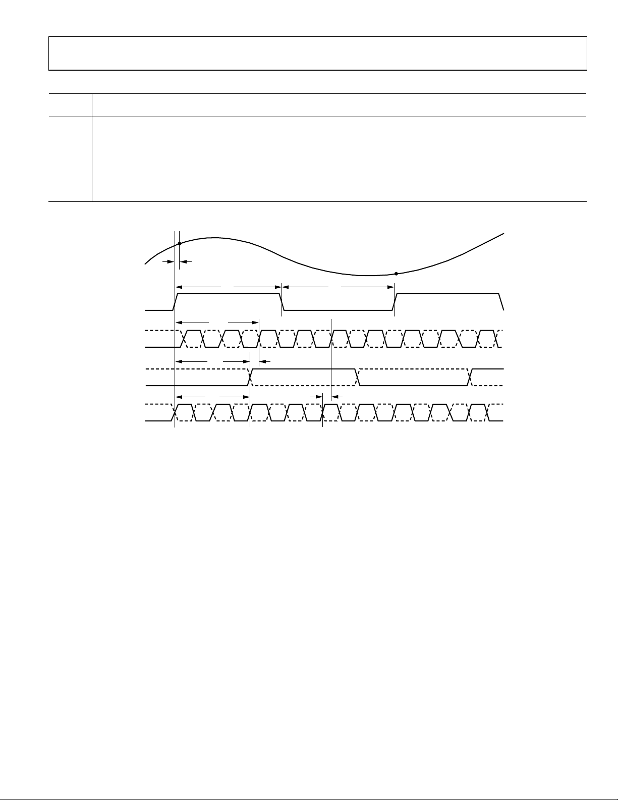
Figure 2. Timing Diagram
Rev. 0 | Page 5 of 16

AD15452
ABSOLUTE MAXIMUM RATINGS
Table 3.
Parameter Rating
AVDD to AGND −0.3 V to +3.9 V
DRVDD to DRGND −0.3 V to +3.9 V
DRGND to AGND −0.3 V to +0.3 V
DRVDD to AVDD −3.9 V to +3.9 V
Analog Inputs −0.3 V to AVDD
Digital Outputs −0.3 V to DRVDD
CLK −0.3 V to AVDD
LVDSBIAS −0.3 V to DRVDD
PDWN, DTP −0.3 V to AVDD
Operational Case Temperature −40°C to +85°C
Storage Temperature Range 65°C to 150°C
Lead Temperature:
Infrared, 15 seconds
230°C
Stresses above those listed under Absolute Maximum Ratings
may cause permanent damage to the device. This is a stress
rating only; functional operation of the device at these or any
other conditions above those indicated in the operational
section of this specification is not implied. Exposure to absolute
maximum rating conditions for extended periods may affect
device reliability.
ESD CAUTION
ESD (electrostatic discharge) sensitive device. Electrostatic charges as high as 4000 V readily accumulate on
the human body and test equipment and can discharge without detection. Although this product features
proprietary ESD protection circuitry, permanent damage may occur on devices subjected to high energy
electrostatic discharges. Therefore, proper ESD precautions are recommended to avoid performance
degradation or loss of functionality.
Rev. 0 | Page 6 of 16
 Loading...