

Quad-SHARC
®
a
PERFORMANCE FEATURES
...
ADSP-21060 Core Processor (
480 MFLOPS Peak, 320 MFLOPS Sustained
25 ns Instruction Rate, Single-Cycle
Instruction Execution–Each of Four Processors
16 Mbit Shared SRAM (Internal to SHARCs)
4 Gigawords Addressable Off-Module Memory
Sixteen 40 Mbyte/s Link Ports (Four per SHARC)
Eight 40 Mbit/s Independent Serial Ports (Two
from Each SHARC)
5 V and 3.3 V Operation
32-Bit Single Precision and 40-Bit Extended
Precision IEEE Floating Point Data Formats, or
32-Bit Fixed Point Data Format
IEEE JTAG Standard 1149.1 Test Access Port and
On-Chip Emulation
PACKAGING FEATURES
452-Lead Ceramic Ball Grid Array (CBGA)
1.85" (47 mm) Body Size
0.200" Max Height
0.050" Ball Pitch
29 Grams (typical)
= 0.368C/W
u
JC
34)
ID
2-0
CPA
SPORT 1
SPORT 0
TDI
AD14160/
AD14160L
ID
2-0
CPA
SPORT 1
SPORT 0
TDO
CS
LINK 1
TIMEXP
SHARC_A
EMU
EBOOT,
LBOOT, BMS
EMU
EBOOT,
LBOOT, BMS
SHARC_D
CS
TIMEXP
LINK 1
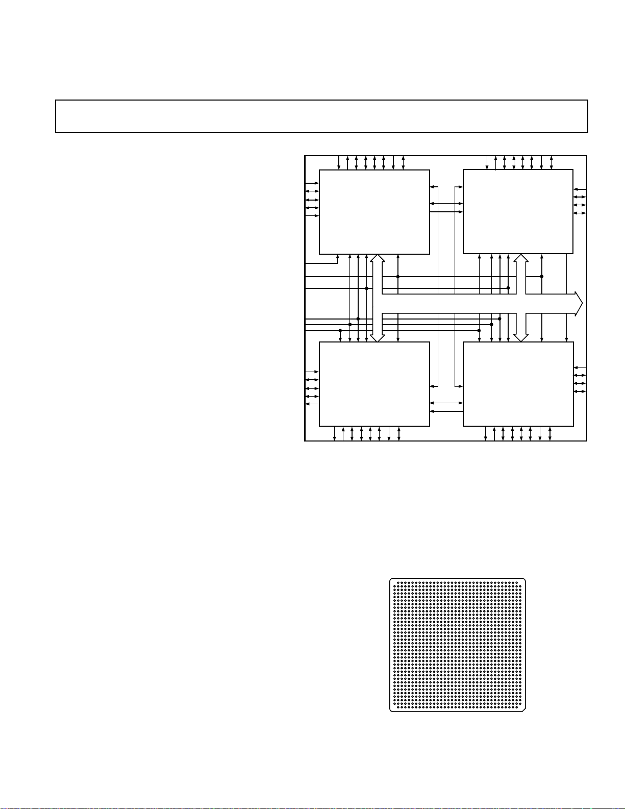
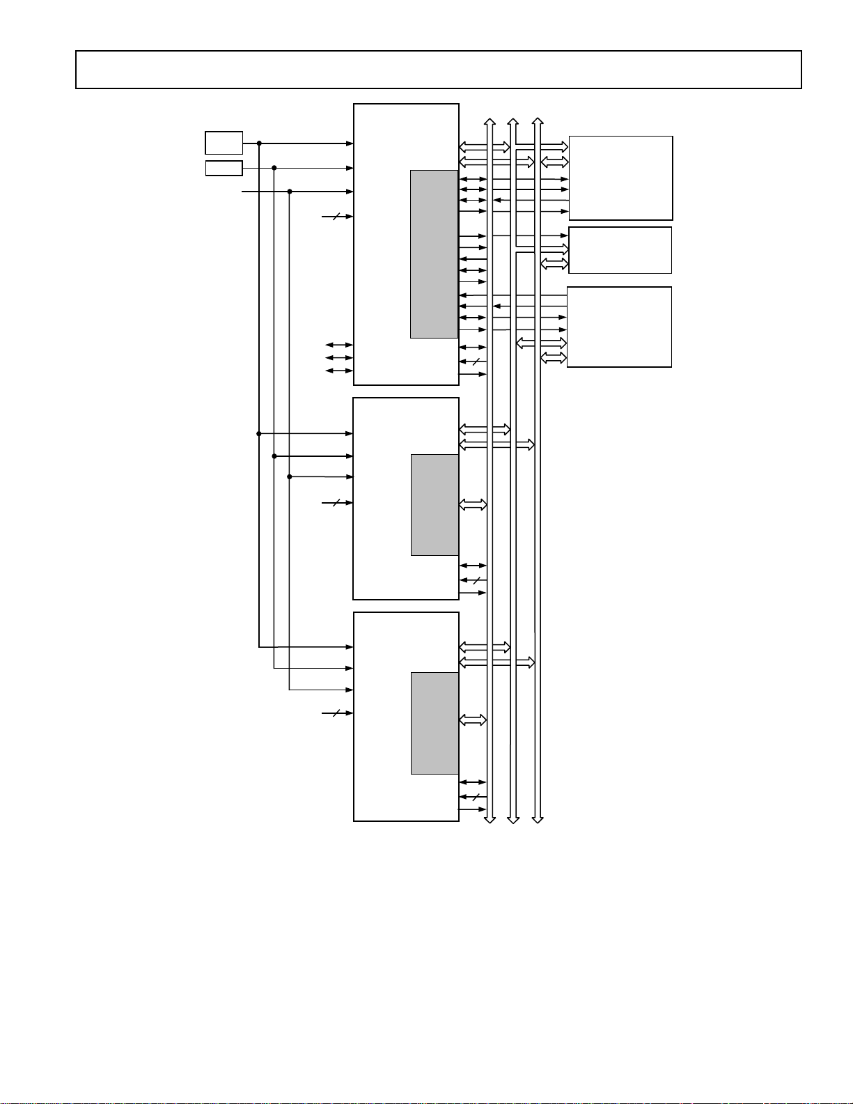
DSP Multiprocessor Family
AD14160/AD14160L
FUNCTIONAL BLOCK DIAGRAM
3-0
2-0
LINK 0
IRQ
LINK 2
LINK 3
LINK 4
FLAG
LINK 5
TDO
CLKIN
RESET
CLKIN
RESET
LINK 2
TCK, TMS, TRST
SHARC BUS (
SBTS, HBR, HBG, REDY, BR
LINK 3
LINK 4
ADDR
LINK 0
TCK, TMS, TRST
LINK 5
3-0
2-0
TDI
IRQ
FLAG
31-0
,
DATA
CS
LINK 0
LINK 5
TDI
47-0
LINK 0
LINK 5
TDO
MS
,
LINK 1
TIMEXP
SHARC_B
EMU
CLKIN
EBOOT,
3-0
EBOOT,
RESET
LBOOT, BMS
,
RD, WR, PAGE, ADRCLK, SW, ACK,
, RPBA, DMAR
6-1
EMU
CLKIN
RESET
LBOOT, BMS
SHARC_C
CS
TIMEXP
LINK 1
LINK 2
LINK 3
LINK 2
LINK 3
2-0
IRQ
LINK 4
SPORT 1
SPORT 0
TCK, TMS, TRST
, DMAG
1.2
1.2
SPORT 1
TCK, TMS, TRST
SPORT 0
2-0
LINK 4
IRQ
3-0
ID
FLAG
CPA
)
ID
CPA
3-0
FLAG
2-0
TDO
TDI
2-0
GENERAL DESCRIPTION
The AD14160/AD14160L Quad-SHARC Ceramic Ball Grid
Array (CBGA) puts the power of the first generation AD14060
(CQFP) DSP multiprocessor into a very high density ball grid
array package; now with additional link and serial I/O pinned
out, beyond that from the CQFP package. The core of the multiprocessor is the ADSP-21060 DSP microcomputer. The AD14x60
modules have the highest performance—density and lowest
cost— performance ratios of any in their class. They are ideal
for applications requiring higher levels of performance and/or
functionality per unit area.
The AD14160/AD14160L takes advantage of the built-in
multiprocessing features of the ADSP-21060 to achieve 480 peak
MFLOPS with a single chip type, in a single package. The onchip SRAM of the DSPs provides 16 Mbits of on-module
shared SRAM. The complete shared bus (48 data, 32 address)
is also brought off-module for interfacing with expansion
memory or other peripherals.
SHARC is a registered trademark of Analog Devices, Inc.
REV. A
Information furnished by Analog Devices is believed to be accurate and
reliable. However, no responsibility is assumed by Analog Devices for its
use, nor for any infringements of patents or other rights of third parties
which may result from its use. No license is granted by implication or
otherwise under any patent or patent rights of Analog Devices.
The ADSP-21060 link ports are interconnected to provide
direct communication among the four SHARCs as well as high
speed off-module access. Internally, links connect the SHARC
in a ring. Externally, each SHARC has a total of 160 Mbytes/s
link port bandwidth.
Multiprocessor performance is enhanced with embedded power
and ground planes, matched impedance interconnect, and optimized signal routing lengths and separation. The fully tested
and ready-to-insert multiprocessor also significantly reduces
board space.
s
s
s
s
One Technology Way, P.O. Box 9106, Norwood, MA 02062-9106, U.S.A.
Tel: 781/329-4700 World Wide Web Site: http://www.analog.com
Fax: 781/326-8703 © Analog Devices, Inc., 1998
AD14160/AD14160L
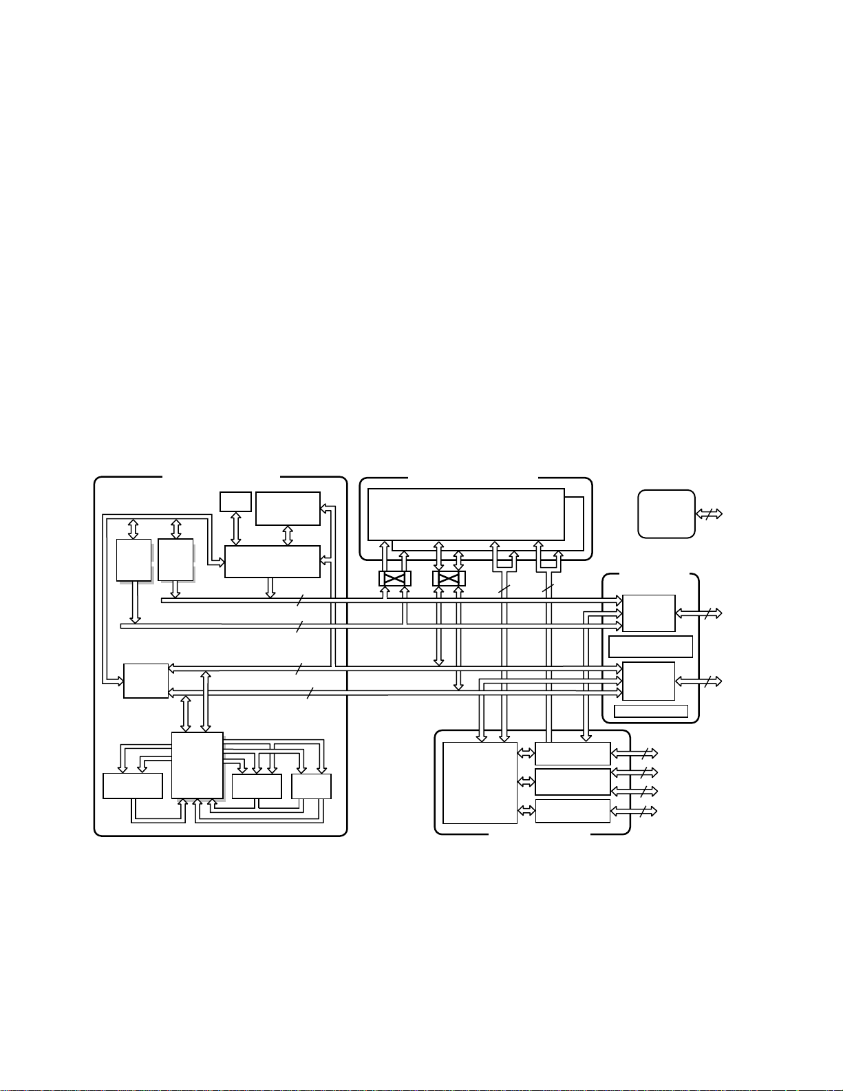
DETAILED DESCRIPTION
Architectural Features
ADSP-21060 Core
The AD14160/AD14160L is based on the powerful ADSP-21060
(SHARC) DSP chip. The ADSP-21060 SHARC combines a
high performance floating-point DSP core with integrated, onchip system features including a 4 Mbit SRAM memory, host
processor interface, DMA controller, serial ports, and both link
port and parallel bus connectivity for glueless DSP multiprocessing, (see Figure 1). It is fabricated in a high speed, low power
CMOS process, and has a 25 ns instruction cycle time. The arithmetic/ logic unit (ALU), multiplier and shifter all perform singlecycle instructions, and the three units are arranged in parallel,
maximizing computational throughput.
The SHARC features an enhanced Harvard architecture in
which the data memory (DM) bus transfers data, and the program memory (PM) bus transfers both instructions and data.
There is also an on-chip instruction cache which selectively
caches only those instructions whose fetches conflict with the
PM bus data accesses. This combines with the separate program
and data memory buses to enable three-bus operation for fetching an instruction and two operands, all in a single cycle. The
SHARC also contains a general purpose data register file, which
CORE PROCESSOR
INSTRUCTION
DAG1
8 x 4 x 32
BUS
CONNECT
(PX)
DAG2
8 x 4 x 24
TIMER
DM ADDRESS BUS
PM DATA BUS
DM DATA BUS
CACHE
32 x 48-BIT
PROGRAM
SEQUENCER
24PM ADDRESS BUS
32
48
40/32
PROCESSOR PORT I/O PORT
ADDR DATA ADDR
ADDR DATA
is a 10-port, 32-register (16 primary, 16 secondary) file. Each
SHARC’s core also implements two data address generators
(DAGs), implementing circular data buffers in hardware. The
DAGs contain sufficient registers to allow the creation of up to
32 circular buffers. The 48-bit instruction word accommodates a
variety of parallel operations, for concise programming. For example, the ADSP-21060 can conditionally execute a multiply, an
add, a subtract, and a branch, all in a single instruction.
The SHARCs contain 4 Mbits of on-chip SRAM each, organized as two blocks of 2 Mbits, which can be configured for
different combinations of code and data storage. The memory
can be configured as a maximum of 128K words of 32-bit data,
256K words of 16-bit data, 80K words of 48-bit instructions (or
40-bit data), or combinations of different word sizes up to
4 megabits. A 16-bit floating-point storage format is supported
which effectively doubles the amount of data that may be stored
on chip. Conversion between the 32-bit floating point and 16bit floating point formats is done in a single instruction. Each
memory block is dual-ported for single-cycle, independent
accesses by the core processor and I/O processor or DMA controller. The dual-ported memory and separate on-chip buses
allow two data transfers from the core and one from I/O, all in a
single cycle.
DUAL-PORTED SRAM
TWO INDEPENDENT
DUAL-PORTED BLOCKS
DATA
DATA
IOD
48
ADDR
IOA
17
BLOCK 0
BLOCK 1
JTAG
TEST AND
EMULATION
EXTERNAL
PORT
ADDR BUS
MUX
MULTIPROCESSOR
INTERFACE
DATA BUS
MUX
HOST PORT
7
32
48
DATA
REGISTER
FILE
16 x 40-BIT
BARREL
SHIFTER
IOP
REGISTERS
(
ALUMULTIPLIER
MEMORY MAPPED)
CONTROL,
STATUS, AND
DATA BUFFERS
DMA
CONTROLLER
SERIAL PORTS
(2)
LINK PORTS
(6)
4
6
6
36
I/O PROCESSOR
Figure 1. ADSP-21060 Processor Block Diagram (Core of the AD14160/AD14160L)
–2–
REV. A
AD14160/AD14160L
INTERNAL
MEMORY
SPACE
(INDIVIDUAL
SHARCs)
MULTIPROCESSOR
MEMORY SPACE
IOP REGISTERS
NORMAL WORD ADDRESSING
SHORT WORD ADDRESSING
INTERNAL MEMORY SPACE
OF SHARC_A
ID=001
INTERNAL MEMORY SPACE
OF SHARC_B
INTERNAL
TO AD14160x
EXTERNAL
TO AD14160x
NORMAL WORD ADDRESSING: 32-BIT DATA WORDS
48-BIT INSTRUCTION WORDS
SHORT WORD ADDRESSING: 16-BIT DATA WORDS
INTERNAL MEMORY SPACE
INTERNAL MEMORY SPACE
INTERNAL MEMORY SPACE
INTERNAL MEMORY SPACE
ID=010
OF SHARC_C
ID=011
OF SHARC_D
ID=100
OF ADSP-2106x
WITH ID=101
OF ADSP-2106x
WITH ID=110
BROADCAST WRITE
TO ALL
ADSP-2106xs
0x0000 0000
0x0002 0000
0x0004 0000
0x0008 0000
0x0010 0000
0x0018 0000
0x0020 0000
0x0028 0000
0x0030 0000
0x0038 0000
0x003F FFFF
EXTERNAL
MEMORY
SPACE
BANK 0
DRAM
(OPTIONAL)
BANK 1
BANK 2
BANK 3
NONBANKED
0x0040 0000
MS
0
MS
1
MS
2
MS
3
BANK SIZE IS
SELECTED BY
MSIZE BIT FIELD OF
SYSCON
REGISTER.
0xFFFF FFFF
Figure 2. AD14160/AD14160L Memory Map
SYSTEM EXPANSION
1X CLOCK
CLKIN
RESET
BOOTSELECT A
BOOTSELECT BCD
DMAR1,2
DMAG1,2
SPORT0
SPORT1
JTAG
SHARC_A
LINKS 1, 2, 3, & 4;
IRQ
2-0
FLAG
TIMEXP,
SPORT1
CPA
ID
-0
2
SHARC_D
LINKS 1, 2, 3, & 4;
IRQ
2-0
FLAG
TIMEXP,
SPORT1
CPA
ID
-0
2
;
;
3-0
(QUAD PROCESSOR
;
;
3-0
SHARC_B
LINKS 1, 2, 3, & 4;
IRQ
2-0
FLAG
TIMEXP,
SPORT1
CPA
ID
-0
2
AD14160/
AD14160L
CLUSTER)
SHARC_C
LINKS 1, 2, 3, & 4;
IRQ
2-0
FLAG
TIMEXP,
SPORT1
CPA
ID
-0
2
ADDR
31-0
DATA
;
;
3-0
;
;
3-0
47-0
RD
WR
ACK
MS
PAGE
SBTS
SW
ADRCLK
CS
HBR
HBG
REDY
BR
RPBA
3-0
1-6
Figure 3. Complete Shared Memory Multiprocessing System
REV. A
–3–
AD14160/AD14160L
Shared Memory Multiprocessing
The AD14160/AD14160L takes advantage of the powerful
multiprocessing features built into the SHARC. The SHARCs are
connected to maximize the performance of this cluster-of-four
architecture, and still allow for off-module expansion. The
AD14160/AD14160L in itself is a complete shared memory
multiprocessing system, as shown in Figure 3. The unified address space of the SHARCs allows direct interprocessor accesses of each SHARCs’ internal memory. In other words, each
SHARC can directly access the internal memory and IOP registers
of each of the other SHARCs by simply reading or writing to the
appropriate address in multi-processor memory space (see Figure 2)—this is called a direct read or direct write.
Bus arbitration is accomplished with the on-SHARC arbitration
logic. Each SHARC has a unique ID, and drives the Bus-Request
(BR) line corresponding to its ID, while monitoring all others.
BR1–BR4 are used within the AD14160/AD14160L, while BR5
and BR6 can be used for expansion. All bus requests (BR1–BR6)
are included in the module I/O.
Two different priority schemes, fixed and rotating, are available
to resolve competing bus requests. The RPBA pin selects which
scheme is used: when RPBA is high, rotating priority bus arbitration is selected, and when RPBA is low, fixed priority is selected.
Table I. Rotating Priority Arbitration Example
Hardware Processor IDs
Cycle ID1 ID2 ID3 ID4 ID5 ID6
1M12 BR345Initial Priority Assignments
2 4 5 BR M-BR 1 2 3
3 4 5 BR M 1 2 3
4 5 BR M 1 2 3 4 BR
51 BR23 45MFinal Priority Assignments
NOTES
1–5 = Assigned Priority.
M = Bus Mastership (in that cycle).
BR = Requesting Bus Mastership with BRx.
Bus mastership is passed from one SHARC to another during a
bus transition cycle. A bus transition cycle only occurs when the
current bus master deasserts its BR line and one of the slave
SHARCs asserts its BR line. The bus master can therefore retain bus mastership by keeping its BR line asserted. When the
bus master deasserts its BR line, and no other BR line is asserted, then the master will not lose any bus cycles. When more
than one SHARC asserts its BR line, the SHARC with the
highest priority request becomes bus master on the following
cycle. Each SHARC observes all of the BR lines, and therefore
tracks when a bus transition cycle has occurred, and which
processor has become the new bus master. Master processor
changeover incurs only one cycle of overhead. An example bus
transition sequence is shown in Table I.
Bus locking is possible, allowing indivisible read-modify-write
sequences for semaphores. In either the fixed or rotating priority
scheme, it is also possible to limit the number of cycles the
master can control the bus. The AD14160/AD14160L also
provides the option of using the Core Priority Access (CPA)
mode of the SHARC. Using the CPA signal allows external bus
accesses by the core processor of a slave SHARC to take priority
over ongoing DMA transfers. Also, each SHARC can broadcast
write to all other SHARCs simultaneously, allowing the implementation of reflective semaphores.
The bus master can communicate with slave SHARCs by writing messages to their internal IOP registers. The MSRG0–
MSRG7 registers are general-purpose registers that can be used
for convenient message passing, semaphores and resource sharing between the SHARCs. For message passing, the master
communicates with a slave by writing and/or reading any of the
eight message registers on the slave. For vector interrupts, the
master can issue a vector interrupt to a slave by writing the
address of an interrupt service routine to the slave’s VIRPT
register. This causes an immediate high priority interrupt on the
slave which, when serviced, will cause it to branch to the specified service routine.
Off-Module Memory and Peripherals Interface
The AD14160/AD14160L’s external port provides the interface to
off-module memory and peripherals (see Figure 5). This port
consists of the complete external port bus of the SHARC, bused
together in common among the four SHARCs.
The 4-gigaword off-module address space is included in the
AD14160/AD14160L’s unified address space. Addressing of
external memory devices is facilitated by each SHARC internally decoding the high order address lines to generate memory
bank select signals. Separate control lines are also generated for
simplified addressing of page-mode DRAM. The AD14160/
AD14160L also supports programmable memory wait states and
external memory acknowledge controls to allow interfacing to
DRAM and peripherals with variable access, hold and disable
time requirements.
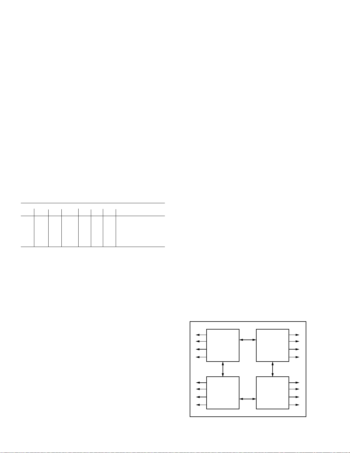
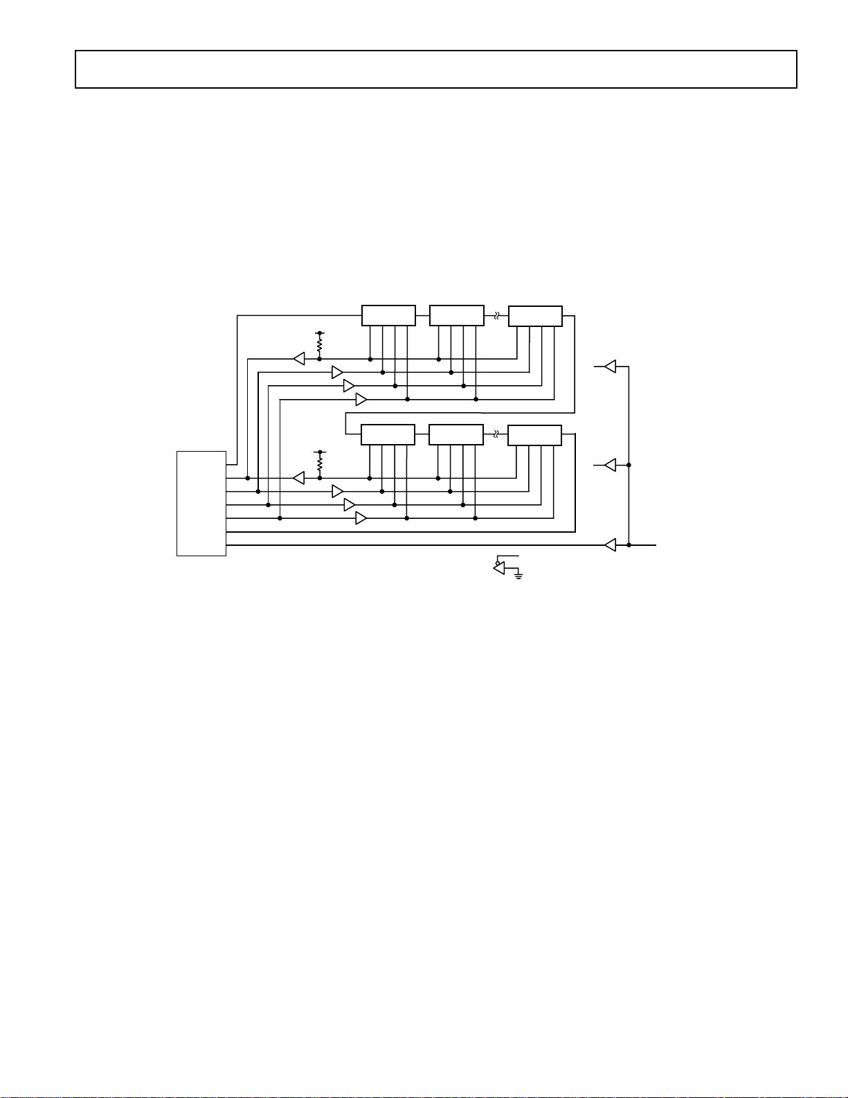
Link Port I/O
Each individual SHARC features six 4-bit link ports that facilitate SHARC-to-SHARC communication and external I/O interfacing. Each link port can be configured for either 1× or 2×
operation, allowing each to transfer either 4 or 8 bits per cycle.
The link ports can operate independently and simultaneously,
with a maximum bandwidth of 40 MBytes/s each, or a total of
240 MBytes/s per SHARC.
The AD14160/AD14160L provides additional link port I/O
beyond that of the AD14060. Internally, two links from each
SHARC form a ring connection among the four. The remaining
four link ports from each SHARC are brought out independently from each SHARC. A maximum of 640 MBytes/s link
port bandwidth is then available off of the AD14160/AD14160L.
The link port connections are detailed in Figure 4.
1
2
SHARC_A SHARC_B
3
4
0
0
1
2
SHARC_D SHARC_C
3
4
55
55
1
2
3
4
0
0
1
2
3
4
Figure 4. Link Port Connections
–4–
REV. A
1x
CLOCK
RESET
CLKIN
RESET
RPBA
3
ID
CONTROL
SERIALS
LINKS
DISCRETES
ADSP-2106x #5
CLKIN
RESET
RPBA
3
ID
AD14160/
AD14160L
ADDR
DATA
ADRCLK
(OPTIONAL)
ADDR
DATA
31–0
47–0
WR
ACK
MS
BMS
PAGE
SBTS
HBR
HBG
REDY
CPA
BR
BR
31–0
47–0
RD
3–0
SW
CS
2–6
AD14160/AD14160L
ADDR
OE
WE
ACK
CS
GLOBAL
MEMORY
AND
PERIPHERALS
(OPTIONAL)
BOOT
EPROM
(OPTIONAL)
HOST
PROCESSOR
INTERFACE
(OPTIONAL)
DATA
CS
ADDR
DATA
5
1
ADDR
DATA
CONTROL
CPA
BR
BR
31–0
47–0
CPA
1–5
BR
5
5
5
6
ADSP-2106x #6
CLKIN
RESET
RPBA
3
ID
CONTROL
BR
1
(OPTIONAL)
ADDR
DATA
, 2, 3, 4, 6
Figure 5. Optional System Interconnections
REV. A
–5–

AD14160/AD14160L
Link port 4, the boot link port, is brought off independently
from each SHARC. Individual booting is then allowed, or
chained link port booting is possible as described under “Link
Port Booting.”
Link port data is packed into 32-bit or 48-bit words, and can be
directly read by the SHARC core processor or DMA-transferred
to on-SHARC memory.
Each link port has its own double-buffered input and output
registers. Clock/acknowledge handshaking controls link port
transfers. Transfers are programmable as either transmit or
receive.
Serial Ports
The SHARC serial ports provide an inexpensive interface to a
wide variety of digital and mixed-signal peripheral devices. Each
SHARC has two serial ports. All eight of the AD14160/AD14160L
serial ports are brought off-module.
The serial ports can operate at the full clock rate of the module,
providing each with a maximum data rate of 40 Mbit/s. Independent transmit and receive functions provide more flexible
communications. Serial port data can be automatically transferred to and from on-SHARC memory via DMA, and each of
the serial ports offers time division multiplexed (TDM) multichannel mode.
The serial ports can operate with little-endian or big-endian
transmission formats, with word lengths selectable from 3 bits to
32 bits. They offer selectable synchronization and transmit
modes as well as optional µ-law or A-law companding. Serial
port clocks and frame syncs can be internally or externally
generated.
Program Booting
The AD14160/AD14160L supports automatic downloading of
programs following power-up or a software reset. The SHARC
offers four options for program booting: 1) from an 8-bit
EPROM; 2) from a host processor; 3) through the link ports;
and 4) no-boot. In no-boot mode, the SHARC starts executing
instructions from address 0x0040 0004 in external memory.
The boot mode is selected by the state of the following signals:
BMS, EBOOT, and LBOOT.
On the AD14160/AD14160L, SHARC_A’s boot mode is separately controlled, while SHARCs B, C, and D are controlled as
a group. With this flexibility, the AD14160/AD14160L can be
configured to boot in any of the following methods.
Multiprocessor Host Booting
To boot multiple ADSP-21060 processors from a host, each
ADSP-21060 must have its EBOOT, LBOOT and BMS pins
configured for host booting: EBOOT = 0, LBOOT = 0, and
BMS = 1. After system power-up, each ADSP-21060 will be in
the idle state and the BRx bus request lines will be deasserted.
The host must assert the HBR input and boot each ADSP-21060
by asserting its CS pin and downloading instructions.
Multiprocessor EPROM Booting
There are two methods of booting the multiprocessor system
from an EPROM.
SHARC_A Is Booted, Which Then Boots the Others. The
EBOOT pin on the SHARC_A must be set high for EPROM
booting. All other ADSP-21060s should be configured for host
booting (EBOOT = 0, LBOOT = 0, and BMS = 1), which
leaves them in the idle state at start-up and allows SHARC_A
to become bus master and boot itself. Only the BMS pin of
SHARC_A is connected to the chip select of the EPROM.
When SHARC_A has finished booting, it can boot the remaining ADSP-21060s by writing to their external port DMA
buffer 0 (EPB0) via multiprocessor memory space.
All ADSP-21060s Boot in Turn From a Single EPROM.
The BMS signals from each ADSP-21060 may be wire-ORed
together to drive the chip select pin of the EPROM. Each
ADSP-21060 can boot in turn, according to its priority. When
the last one has finished booting, it must inform the others (which
may be in the idle state) that program execution can begin.
Multiprocessor Link Port Booting
Booting can also be accomplished from a single source through
the link ports. Link Buffer 4 must always be used for booting.
To simultaneously boot all of the ADSP-21060s, a parallel
common connection is available through Link Port 4 on each of
the processors. Or, using the daisy chain connection that exists
between the processors’ link ports, each ADSP-21060 can boot
the next one in turn. In this case, the Link Assignment Register
(LAR) must be programmed to configure the internal link ports
with Link Buffer 4.
Multiprocessor Booting From External Memory
If external memory contains a program after reset, then
SHARC_A should be set up for no boot mode; it will begin executing from address 0x0040 0004 in external memory. When
booting has completed, the other ADSP-21060s may be booted
by SHARC_A if they are set up for host booting, or they can
begin executing out of external memory if they are set up for no
boot mode. Multiprocessor bus arbitration will allow this booting
to occur in an orderly manner.
Host Processor Interface
The AD14160/AD14160L’s host interface allows for easy connection to standard microprocessor buses, both 16-bit and 32bit, with little additional hardware required. Asynchronous
transfers at speeds up to the full clock rate of the module are
supported. The host interface is accessed through the AD14160/
AD14160L external port and is memory-mapped into the unified address space. Four channels of DMA are available for the
host interface; code and data transfers are accomplished with
low software overhead.
The host processor requests the AD14160/AD14160L’s external
bus with the host bus request (HBR), host bus grant (HBG),
and ready (REDY) signals. The host can directly read and write
the internal memory of the SHARCs, and can access the DMA
channel setup and mailbox registers. Vector interrupt support is
provided for efficient execution of host commands.
Direct Memory Access (DMA) Controller
The SHARCs on-chip DMA control logic allows zero-overhead data transfers without processor intervention. The DMA
controller operates independently and invisibly to each SHARCs
processor core, allowing DMA operations to occur while the core
is simultaneously executing its program instructions.
DMA transfers can occur between SHARC internal memory
and either external memory, external peripherals, or a host
processor. DMA transfers can also occur between the SHARC’s
internal memory and its serial ports or link ports. DMA transfers between external memory and external peripheral devices are
another option. External bus packing to 16-, 32- or 48-bit words
is performed during DMA transfers.
–6–
REV. A

AD14160/AD14160L
Ten channels of DMA are available on the SHARCs—two via
the link ports, four via the serial ports, and four via the processor’s
external port (for either host processor, other SHARCs, memory,
or I/O transfers). Four additional link port DMA channels are
shared with serial port 1 and the external port. Programs can be
downloaded to the SHARCs using DMA transfers. Asynchronous off-module peripherals can control two DMA channels
using DMA Request/Grant lines (DMAR1-2, DMAG1-2).
Other DMA features include interrupt generation upon completion of DMA transfers and DMA chaining for automatic linked
DMA transfers.
Development Tools
The AD14160/AD14160L is supported with a complete set
of software and hardware development tools, including an
EZ-LAB
®
In-Circuit Emulator, and development software.
Analog Devices’ ADSP-21000 Family Development Software
includes an easy to use Assembler based on an algebraic syntax,
an Assembly Library/Librarian, a Linker, an Instruction-Level
Simulator, an ANSI C optimizing Compiler, the CBug™ C
Source-Level Debugger, and a C Runtime Library including
DSP and mathematical functions. The Optimizing Compiler
includes Numerical C extensions based on the work of the ANSI
Numerical C Extensions Group. Numerical C provides extensions to the C language for array selection, vector math operations, complex data types, circular pointers and variably
dimensioned arrays. The ADSP-21000 Family Development
Software is available for both the PC and Sun platforms.
The SHARC EZ-KIT combines the ADSP-21000 Family Development Software for the PC and the EZ-LAB Development
Board in one package.
The ADSP-2106x EZ-ICE
®
Emulator uses the IEEE 1149.1
JTAG test access port of the ADSP-2106x processor to monitor
and control the target board processor during emulation. The
EZ-ICE provides full-speed emulation, allowing inspection and
modification of memory, registers and processor stacks.
Nonintrusive in-circuit emulation is assured by the use of the
processor’s JTAG interface—the emulator does not affect target
system loading or timing.
Further details and ordering information are available in the
ADSP-21000 Family Hardware & Software Development Tools
data sheet (ADDS-2100xx-TOOLS). This data sheet can be
requested from any Analog Devices sales office or distributor,
or from the Literature Center.
In addition to the software and hardware development tools
available from Analog Devices, third parties provide a wide
range of tools supporting the SHARC processor family. Hardware tools include SHARC PC plug-in cards, multiprocessor
SHARC VME boards, and daughter card modules with multiple
SHARCs and additional memory. These modules are based on
the SHARCPAC™ module specification. Third party software
tools include an Ada compiler, DSP libraries, operating systems
and block diagram design tools.
Other Package Details
The AD14160/AD14160L contains 14 on-module 0.1 microfarad bypass capacitors. It is recommended that in the target
system at least four additional capacitors, of 0.018 microfarad
value, be placed around the module—one near each of the four
corners.
The top surface, lid, of the AD14160/AD14160L is electrically
connected to GND.
Additional Information
This data sheet provides a general overview of the AD14160/
AD14160L architecture and functionality. For detailed information on the ADSP-2106x SHARC and the ADSP-21000
Family core architecture and instruction set, refer to the
ADSP-2106x SHARC User’s Manual.
EZ-ICE and EZ-LAB are registered trademarks of Analog Devices, Inc.
CBug and SHARCPAC are trademarks of Analog Devices, Inc.
REV. A
–7–

AD14160/AD14160L
PIN FUNCTION DESCRIPTIONS
AD14160/AD14160L pin definitions are listed below. Inputs
identified as synchronous (S) must meet timing requirements
with respect to CLKIN (or with respect to TCK for TMS,
TDI). Inputs identified as asynchronous (A) can be asserted
asynchronously to CLKIN (or to TCK for TRST).
Unused inputs should be tied or pulled to V
for ADDR
, DATA
31-0
, FLAG
47-0
, SW, and inputs that have
2-0
or GND, except
DD
TCLKx, RCLKx, LxDAT
TDI)—these pins can be left floating. These pins have a logiclevel hold circuit that prevents the input from floating internally.
A = Asynchronous O = Output (A/D) = Active Drive
G = Ground P = Power Supply (O/D) = Open Drain
I = Input S = Synchronous
T = Three-State (when SBTS is asserted, or when the AD14160/
AD14160L is a bus slave)
, LxCLK, LxACK, TMS and
3-0
internal pull-up or pull-down resistors (CPA, ACK, DTx, DRx,
Pin Type Function
ADDR
31-0
I/O/T External Bus Address. (Common to all SHARCs) The AD14160/AD14160L outputs addresses for
external memory and peripherals on these pins. In a multiprocessor system, the bus master outputs addresses for read/writes on the internal memory or IOP registers of slave ADSP-2106xs. The AD14160/
AD14160L inputs addresses when a host processor or multiprocessing bus master is reading or writing
the internal memory or IOP registers of internal ADSP-21060s.
DATA
47-0
I/O/T External Bus Data. (Common to all SHARCs) The AD14160/AD14160L inputs and outputs data and
instructions on these pins. 32-bit single-precision floating-point data and 32-bit fixed-point data is transferred over bits 47-16 of the bus. 40-bit extended-precision floating-point data is transferred over bits 478 of the bus. 16-bit short word data is transferred over bits 31-16 of the bus. In PROM boot mode, 8-bit
data is transferred over bits 23-16. Pull-up resistors on unused DATA pins are not necessary.
MS
3-0
O/T Memory Select Lines. (Common to all SHARCs) These lines are asserted (low) as chip selects for the
corresponding banks of external memory. Memory bank size must be defined in the individual ADSP21060’s system control registers (SYSCON). The MS
change at the same time as the other address lines. When no external memory access is occurring the MS
lines are decoded memory address lines that
3-0
3-0
lines are inactive; they are active, however, when a conditional memory access instruction is executed, whether
or not the condition is true. MS
(Bank 0). In a multiprocessing system, the MS
can be used with the PAGE signal to implement a bank of DRAM memory
0
lines are output by the bus master.
3-0
RD I/O/T Memory Read Strobe. (Common to all SHARCs) This pin is asserted (low) when the AD14160/
AD14160L reads from external devices or when the internal memory of internal ADSP-2106xs is being
accessed. External devices (including other ADSP-2106xs) must assert RD to read from the AD14160/
AD14160L’s internal memory. In a multiprocessing system, RD is output by the bus master and is input
by all other ADSP-2106xs.
WR I/O/T Memory Write Strobe. (Common to all SHARCs) This pin is asserted (low) when the AD14160/
AD14160L writes to external devices or when the internal memory of internal ADSP-2106xs is being
accessed. External devices (including other ADSP-2106xs) must assert WR to write to the AD14160/
AD14160L’s internal memory. In a multiprocessing system WR is output by the bus master and is input by all
other ADSP-2106xs.
PAGE O/T DRAM Page Boundary. (Common to all SHARCs) The AD14160/AD14160L asserts this pin to signal
that an external DRAM page boundary has been crossed. DRAM page size must be defined in the individual ADSP-21060’s memory control register (WAIT). DRAM can only be implemented in external
memory Bank 0; the PAGE signal can only be activated for Bank 0 accesses. In a multiprocessing system,
PAGE is output by the bus master.
ADRCLK O/T Clock Output Reference. (Common to all SHARCs) In a multiprocessing system, ADRCLK is output
by the bus master.
SW I/O/T Synchronous Write Select. (Common to all SHARCs) This signal is used to interface the AD14160/
AD14160L to synchronous memory devices (including other ADSP-2106xs). The AD14160/AD14160L
asserts SW (low) to provide an early indication of an impending write cycle, which can be aborted if WR
is not later asserted (e.g., in a conditional write instruction). In a multiprocessing system, SW is output
by the bus master and is input by all other ADSP-2106xs to determine if the multiprocessor memory
access is a read or write. SW is asserted at the same time as the address output. A host processor using
synchronous writes must assert this pin when writing to the AD14160/AD14160L.
ACK I/O/S Memory Acknowledge. (Common to all SHARCs) External devices can deassert ACK (low) to add
wait states to an external memory access. ACK is used by I/O devices, memory controllers, or other peripherals to hold off completion of an external memory access. The AD14160/AD14160L deasserts ACK,
as an output, to add wait states to a synchronous access of its internal memory. In a multiprocessing
system, a slave ADSP-2106x deasserts the bus master’s ACK input to add wait state(s) to an access of its
internal memory. The bus master has a keeper latch on its ACK pin that maintains the input at the level
it was last driven to.
–8–
REV. A
AD14160/AD14160L
Pin Type Function
SBTS I/S Suspend Bus Three-State. (Common to all SHARCs) External devices can assert SBTS (low) to
place the external bus address, data, selects, and strobes in a high impedance state for the following cycle.
If the AD14160/AD14160L attempts to access external memory while SBTS is asserted, the processor
will halt and the memory access will not be completed until SBTS is deasserted. SBTS should only be
used to recover from host processor/AD14160/AD14160L deadlock, or used with a DRAM controller.
HBR I/A Host Bus Request. (Common to all SHARCs) Must be asserted by a host processor to request control
of the AD14160/AD14160L’s external bus. When HBR is asserted in a multiprocessing system, the
ADSP-2106x that is bus master will relinquish the bus and assert HBG. To relinquish the bus, the
ADSP-2106x places the address, data, select, and strobe lines in a high impedance state. HBR has priority
over all ADSP-2106x bus requests (BR
HBG I/O Host Bus Grant. (Common to all SHARCs) Acknowledges an HBR bus request, indicating that the
host processor may take control of the external bus. HBG is asserted (held low) by the AD14160/
AD14160L until HBR is released. In a multiprocessing system, HBG is output by the ADSP-2106x bus
master and is monitored by all others.
CSA I/A Chip Select. Asserted by host processor to select SHARC_A.
CSB I/A Chip Select. Asserted by host processor to select SHARC_B.
CSC I/A Chip Select. Asserted by host processor to select SHARC_C.
CSD I/A Chip Select. Asserted by host processor to select SHARC_D.
REDY (O/D) O Host Bus Acknowledge. (Common to all SHARCs) The AD14160/AD14160L deasserts REDY (low)
to add wait states to an asynchronous access of its internal memory or IOP registers by a host. Open drain
output (O/D) by default; can be programmed in ADREDY bit of SYSCON register of individual ADSP21060s to be active drive (A/D). REDY will only be output if the CS and HBR inputs are asserted.
BR
6-1
I/O/S Multiprocessing Bus Requests. (Common to all SHARCs) Used by multiprocessing ADSP-2106xs to
arbitrate for bus mastership. An ADSP-2106x only drives its own BRx line (corresponding to the value of
its ID2-0 inputs) and monitors all others. In a multiprocessor system with less than six ADSP-2106xs, the
unused BRx pins should be pulled high; BR
IDy2-0 I Multiprocessing ID. (Individual ID2–0 from y = SHARC_A, SHARC_B, SHARC_C, SHARC_D.)
Determines which multiprocessing bus request (BR1–BR6) is used by individual ADSP-2106x’s. ID =
001 corresponds to BR1, ID = 010 corresponds to BR2, etc. ID = 000 is reserved for single processor
systems. These lines are a system configuration selection, which should be hardwired or only changed at
reset.
RPBA I/S Rotating Priority Bus Arbitration Select. (Common to all SHARCs) When RPBA is high, rotating
priority for multiprocessor bus arbitration is selected. When RPBA is low, fixed priority is selected. This
signal is a system configuration selection that must be set to the same value on every ADSP-2106x. If the
value of RPBA is changed during system operation, it must be changed in the same CLKIN cycle on
every ADSP-2106x.
CPAy (O/D) I/O Core Priority Access. (y = SHARC_A, B, C, D) Asserting its CPA pin allows the core processor of an
ADSP-2106x bus slave to interrupt background DMA transfers and gain access to the external bus.
CPA is an open drain output that is connected to all ADSP-2106x in the system if this function is
required. The CPA pin of each internal ADSP-21060 is brought out individually. The CPA pin has
an internal 5 kΩ pull-up resistor. If core access priority is not required in a system, the CPA pin
should be left unconnected.
DTy0 O/T Data Transmit (Serial Port 0 individual from SHARC_A, SHARC_B, SHARC_C, SHARC_D). DT
pin has a 50 kΩ internal pull-up resistor.
DRy0 I Data Receive (Serial Port 0 individual from SHARC_A, SHARC_B, SHARC_C, SHARC_D). DR pin
has a 50 kΩ internal pull-up resistor.
TCLKy0 I/O Transmit Clock (Serial Port 0 individual from SHARC_A, SHARC_B, SHARC_C, SHARC_D).
TCLK pin has a 50 kΩ internal pull-up resistor.
RCLKy0 I/O Receive Clock (Serial Port 0 individual from SHARC_A, SHARC_B, SHARC_C, SHARC_D). RCLK
pin has a 50 kΩ internal pull-up resistor.
TFSy0 I/O Transmit Frame Sync (Serial Port 0 individual from SHARC_A, SHARC_B, SHARC_C, SHARC_D).
RFSy0 I/O Receive Frame Sync (Serial Port 0 individual from SHARC_A, SHARC_B, SHARC_C, SHARC_D).
) in a multiprocessing system.
6-1
must not be pulled high or low because they are outputs.
4-1
REV. A
–9–

AD14160/AD14160L
Pin Type Function
DTy1 O/T Data Transmit (Serial Port 1 individual from SHARC_A, SHARC_B, SHARC_C, SHARC_D) DT pin
has a 50 kΩ internal pull-up resistor.
DRy1 I Data Receive (Serial Port 1 individual from SHARC_A, SHARC_B, SHARC_C, SHARC_D) DR pin
has a 50 kΩ internal pull-up resistor.
TCLKy1 I/O Transmit Clock (Serial Port 1 individual from SHARC_A, SHARC_B, SHARC_C, SHARC_D) TCLK
pin has a 50 kΩ internal pull-up resistor.
RCLKy1 I/O Receive Clock (Serial Port 1 individual from SHARC_A, SHARC_B, SHARC_C, SHARC_D) RCLK
pin has a 50 kΩ internal pull-up resistor.
TFSy1 I/O Transmit Frame Sync (Serial Port 1 individual from SHARC_A, SHARC_B, SHARC_C, SHARC_D)
RFSy1 I/O Receive Frame Sync (Serial Port 1 individual from SHARC_A, SHARC_B, SHARC_C, SHARC_D)
FLAGy3-0 I/O/A Flag Pins. (Individual FLAG3-0 from y = SHARC_A, SHARC_B, SHARC_C, SHARC_D) Each is
configured via control bits as either an input or output. As an input, it can be tested as a condition. As an
output, it can be used to signal external peripherals.
IRQy2-0 I/A Interrupt Request Lines. (Individual IRQ2-0 from y = SHARC_A, SHARC_B, SHARC_C, SHARC_D)
May be either edge-triggered or level-sensitive.
DMAR1 I/A DMA Request 1 (DMA Channel 7). Common to SHARC_A, SHARC_B, SHARC_C, SHARC_D.
DMAR2 I/A DMA Request 2 (DMA Channel 8). Common to SHARC_A, SHARC_B, SHARC_C, SHARC_D.
DMAG1 O/T DMA Grant 1 (DMA Channel 7). Common to SHARC_A, SHARC_B, SHARC_C, SHARC_D.
DMAG2 O/T DMA Grant 2 (DMA Channel 8). Common to SHARC_A, SHARC_B, SHARC_C, SHARC_D.
LyxCLK I/O Link Port Clock (y = SHARC_A, B, C, D; x = Link Ports 1, 2, 3, 4)
internal pull-down resistor which is enabled or disabled by the LPDRD bit of the LCOM register, of the
ADSP-20160.
LyxDAT3-0 I/O Link Port Data (y = SHARC_A, B, C, D; x = Link Ports 1, 2, 3, 4)
50 kΩ internal pull-down resistor which is enabled or disabled by the LPDRD bit of the LCOM register,
of the ADSP-21060.
LyxACK I/O Link Port Acknowledge (y = SHARC_A, B, C, D; x = Link Ports 1, 2, 3, 4)
50 kΩ internal pull-down resistor which is enabled or disabled by the LPDRD bit of the LCOM register,
of the ADSP-21060.
EBOOTA I EPROM Boot Select. (SHARC_A) When EBOOTA is high, SHARC_A is configured for booting from
an 8-bit EPROM. When EBOOTA is low, the LBOOTA and BMSA inputs determine booting mode for
SHARC_A. See the following table. This signal is a system configuration selection which should be hardwired.
LBOOTA I Link Boot. When LBOOTA is high, SHARC_A is configured for link port booting. When LBOOTA is
low, SHARC_A is configured for host processor booting or no booting. See the following table. This
signal is a system configuration selection which should be hardwired.
BMSA I/O/T
2
Boot Memory Select. Output: Used as chip select for boot EPROM devices (when EBOOTA = 1,
LBOOTA = 0). In a multiprocessor system, BMS is output by the bus master. Input: When low, indicates
that no booting will occur and that SHARC_A will begin executing instructions from external memory.
See the following table. This input is a system configuration selection which should be hardwired.
EBOOTBCD I EPROM Boot Select. (Common to SHARC_B, SHARC_C, SHARC_D) When EBOOTBCD is high,
SHARC_B, C, D are configured for booting from an 8-bit EPROM. When EBOOTBCD is low, the
LBOOTBCD and BMSBCD inputs determine booting mode for SHARC_B, C and D. See the following
table. This signal is a system configuration selection which should be hardwired.
LBOOTBCD I LINK Boot. (Common to SHARC_B, SHARC_C, SHARC_D) When LBOOTBCD is high, SHARC_B, C,
D are configured for link port booting. When LBOOTBCD is low, SHARC_B, C, D are configured for
host processor booting or no booting. See the following table. This signal is a system configuration selection which should be hardwired.
1
. Each LyxCLK pin has a 50 kΩ
1
. Each LyxDAT pin has a
1
. Each LyxACK pin has a
–10–
REV. A
AD14160/AD14160L
Pin Type Function
2
BMSBCD I/O/T
TIMEXPy O Timer Expired. (Individual TIMEXP from y = SHARC_A, SHARC_B, SHARC_C, SHARC_D) Asserted
CLKIN I Clock In. (Common to all SHARCs) External clock input to the AD14160/AD14160L. The instruction
RESET I/A Module Reset. (Common to all SHARCs) Resets the AD14160/AD14160L to a known state. This input
TCK I Test Clock (JTAG). (Common to all SHARCs) Provides an asynchronous clock for JTAG boundary
TMS I/S Test Mode Select (JTAG). (Common to all SHARCs) Used to control the test state machine. TMS has
TDI I/S Test Data Input (JTAG). Provides serial data for the boundary scan logic chain starting at SHARC_A.
TDO O Test Data Output (JTAG). Serial scan output of the boundary scan chain path, from SHARC_D.
TRST I/A Test Reset (JTAG). (Common to all SHARCs) Resets the test state machine. TRST must be asserted
EMU (O/D) O Emulation Status. (Common to all SHARCs) Must be connected to the ADSP-2106x EZ-ICE target
V
DD
P Power Supply. Nominally +5.0 V dc for 5 V devices or +3.3 V dc for 3.3 V devices (50 pins).
GND G Power Supply Return. (64 pins).
NOTES
1
LINK PORTS 0 and 5 are connected internally as described earlier in Link Port I/O.
2
Three-statable only in EPROM boot mode (when BMS is an output).
Boot Memory Select. Output: Used as chip select for boot EPROM devices (when EBOOTBCD = 1,
LBOOTBCD = 0). In a multiprocessor system, BMS is output by the bus master. Input: When low,
indicates that no booting will occur and that SHARC_B, C, D will begin executing instructions from
external memory. See table below. This input is a system configuration selection which should be
hardwired.
EBOOT LBOOT BMS Booting Mode
1 0 Output EPROM (Connect BMS to EPROM chip select)
0 0 1 (Input) Host Processor
0 1 1 (Input) Link Port
0 0 0 (Input) No Booting. Processor executes from external memory.
0 1 0 (Input) Reserved
1 1 x (Input) Reserved
for four cycles when the timer is enabled and TCOUNT decrements to zero.
cycle rate is equal to CLKIN. CLKIN may not be halted, changed, or operated below the minimum specified
frequency.
must be asserted (low) at power-up.
scan.
a 20 kΩ internal pull-up resistor.
TDI has a 20 kΩ internal pull-up resistor.
(pulsed low) after power-up or held low for proper operation of the AD14160/AD14160L. TRST has a
20 kΩ internal pull-up resistor.
board connector only.
REV. A
–11–
AD14160/AD14160L
TARGET BOARD CONNECTOR FOR EZ-ICE PROBE
The ADSP-2106x EZ-ICE Emulator uses the IEEE 1149.1
JTAG test access port of the ADSP-2106x to monitor and control the target board processor during emulation. The EZ-ICE
probe requires that the AD14160/AD14160L’s CLKIN (optional), TMS, TCK, TRST, TDI, TDO, EMU and GND signals
be made accessible on the target system via a 14-pin connector
(a pin strip header) such as that shown in Figure 6. The EZICE probe plugs directly onto this connector for chip-on-board
emulation. You must add this connector to your target board
design if you intend to use the ADSP-2106x EZ-ICE. The
length of the traces between the connector and the AD14160/
AD14160L’s JTAG pins should be as short as possible.
GND
KEY (NO PIN)
BTMS
BTCK
BTRST
BTDI
GND
12
34
56
78
910
9
11 12
13 14
TOP VIEW
EMU
CLKIN (OPTIONAL)
TMS
TCK
TRST
TDI
TDO
Figure 6. Target Board Connector for ADSP-2106x EZ-ICE
Emulator (Jumpers in Place)
The 14-pin, 2-row pin strip header is keyed at the Pin 3 location;
Pin 3 must be removed from the header. The pins must be
0.025 inch square and at least 0.20 inch in length. Pin spacing
should be 0.1 × 0.1 inches. Pin strip headers are available from
vendors such as 3M, McKenzie and Samtec.
The BTMS, BTCK, BTRST and BTDI signals are provided so
that the test access port can also be used for board-level testing.
When the connector is not being used for emulation, place
jumpers between the Bxxx pins and the xxx pins as shown in
Figure 6. If you are not going to use the test access port for
board testing, tie BTRST to GND and tie or pull up BTCK to
V
. The TRST pin must be asserted after power-up (through
DD
BTRST on the connector) or held low for proper operation of
the AD14160/AD14160L. None of the Bxxx pins (Pins 5, 7, 9,
11) are connected on the EZ-ICE probe.
The JTAG signals are terminated on the EZ-ICE probe as follows:
Signal Termination
TMS Driven through 22 Ω Resistor (16 mA/3.2 mA Driver)
TCK Driven at 10 MHz through 22 Ω Resistor (16 mA/
3.2 mA Driver)
TRST Driven by Open-Drain Driver* (Pulled Up by On-Chip
20 kΩ Resistor)
TDI Driven by 16 mA/3.2 mA Driver
TDO One TTL Load, No Termination
CLKIN One TTL Load, No Termination (Optional Signal)
EMU 4.7 kΩ Pull-Up Resistor, One TTL Load (Open-Drain
Output from ADSP-2106x)
*TRST is driven low until the EZ-ICE probe is turned on by the EZ-ICE
software (after the invocation command).
Figure 7 shows JTAG scan path connections for the multiprocessor system.
OTHER
JTAG
CONTROLLER
EZ-ICE
JTAG
CONNECTOR
TCK
TMS
EMU
TRST
TDO
CLKIN
TDI
SHARC_A
TDI TDO
TCK
TMS
OPTIONAL
EMU
TRST
SHARC_B
TDI TDO
TCK
TMS
EMU
TRST
SHARC_C
TDI TDO
TCK
TMS
EMU
TRST
SHARC_D
TDI TDO
TCK
TMS
EMU
TRST
Figure 7. JTAG Scan Path Connections for the AD14160/AD14160L
JTAG DEVICE
(OPTIONAL)
TDI TDO
TCK
TMS
TRST
ADSP-2106x
#n
TDI TDO
TCK
TMS
EMU
TRST
–12–
REV. A
AD14160/AD14160L
Connecting CLKIN to Pin 4 of the EZ-ICE header is optional.
The emulator only uses CLKIN when directed to perform operations such as starting, stopping and single-stepping multiple
ADSP-2106xs in a synchronous manner. If you do not need
these operations to occur synchronously on the multiple processors, simply tie Pin 4 of the EZ-ICE header to ground.
If synchronous multiprocessor operations are needed and
CLKIN is connected, clock skew between the AD14160/
AD14160L and the CLKIN pin on the EZ-ICE header must be
minimal. If the skew is too large, synchronous operations may
be off by one cycle between processors. For synchronous multiprocessor operation TCK, TMS, CLKIN and EMU should be
TDI TDO TDI TDO
5kV
*
TDI
EMU
TCK
TMS
TRST
TDO
CLKIN
TDI TDO
5kV
*
*
OPEN DRAIN DRIVER OR EQUIVALENT, i.e.,
TDI
treated as critical signals in terms of skew, and should be laid
out as short as possible on your board. If TCK, TMS and
CLKIN are driving a large number of ADSP-2106xs (more than
eight) in your system, then treat them as a “clock tree” using
multiple drivers to minimize skew. (See Figure 8 JTAG Clock
Tree and Clock Distribution in the “High Frequency Design
Considerations” section of the ADSP-2106x User’s Manual).
If synchronous multiprocessor operations are not needed (i.e.,
CLKIN is not connected), just use appropriate parallel termination on TCK and TMS. TDI, TDO, EMU and TRST are not
critical signals in terms of skew.
TDI TDO
TDO
TDI
EMU
TDO
SYSTEM
CLKIN
Figure 8. JTAG Clocktree for Multiple ADSP-2106x Systems
REV. A
–13–
AD14160/AD14160L–SPECIFICATIONS
RECOMMENDED OPERATING CONDITIONS
Parameter Min Max Min Max Units
B Grade K Grade
V
T
DD
CASE
Supply Voltage (5 V) 4.75 5.25 4.75 5.25 V
Supply Voltage (3.3 V) 3.15 3.6 3.15 3.6 V
Case Operating Temperature –40 +100 0 +85 °C
ELECTRICAL CHARACTERISTICS (5 V, 3.3 V SUPPLY)
Parameter Temp Level Test Condition Min Typ Max Min Typ Max Units
V
IH1
V
IH2
V
IL
V
OH
V
OL
I
IH
I
IHX4
I
IL
I
ILX4
I
ILP
I
ILPX4
I
OZH
I
OZHX4
I
OZL
I
OZLX4
I
OZHP
I
OZLC
I
OZLAR
I
OZLA
I
OZLS
I
DDIN
I
DDIDLE
C
IN
High Level Input Voltage
High Level Input Voltage
Low Level Input Voltage
High Level Output Voltage
Low Level Output Voltage
High Level Input Current
High Level Input Current
Low Level Input Current
Low Level Input Current
Low Level Input Current
Low Level Input Current
Three-State Leakage Current
Three-State Leakage Current
Three-State Leakage Current
Three-State Leakage Current
Three-State Leakage Current
Three-State Leakage Current
Three-State Leakage Current
Three-State Leakage Current
Three-State Leakage Current
Supply Current (Internal)
Supply Current (Idle)
Input Capacitance
1
2
1, 2
3, 4
3, 4
5, 6
7, 8
5
7
6
8
9, 10, 11
12
9, 13
12
13
14
11
15
10
16
17
18, 19
EXPLANATION OF TEST LEVELS
Test Level
I 100% Production Tested
20
.
II 100% Production Tested at +25°C, and Sample Tested at Specified Temperatures.
III Sample Tested Only.
IV Parameter is guaranteed by design and analysis, and characterization testing on discrete SHARCs.
V Parameter is typical value only.
VI All devices are 100% production tested at +25°C; sample tested at temperature extremes.
NOTES
1
Applies to input and bidirectional pins: DATA
RPBA, CPAy, TFSy0, TFSy1, RFSy0, RFSy1, LyxDAT
TDI, TCK, HBR, DRy0, DRy1, TCLKy0, TCLKy1, RCLKy0, RCLKy1.
2
Applies to input pins: CLKIN, RESET, TRST.
3
Applies to output and bidirectional pins: DATA
DMAG2, BR
BMSBCD, TDO, EMU.
4
See Output Drive Currents for typical drive current capabilities.
5
Applies to input pins: IRQy
6
Applies to input pins with internal pull-ups: DRy0, DRy1, TDI.
7
Applies to bussed input pins: SBTS, HBR, DMAR1, DMAR2, RPBA, EBOOTBCD, LBOOTBCD, CLKIN, RESET, TCK.
8
Applies to bussed input pins with internal pull-ups: TRST, TMS.
9
Applies to three-statable pins: FLAGy0-3, BMSA, TDO.
10
Applies to three-statable pins with internal pull-ups: DTy0, TCLKy0, RCLKy0, DTy1, TCLKy1, RCLKy1.
11
Applies to ACK pin when pulled up. (Note that ACK is pulled up internally with 2 kΩ during reset in a multiprocessor system, when ID
ADSP-2106x is not requesting bus mastership.)
12
Applies to bussed three-statable pins: DATA
that ACK is pulled up internally with 2 kΩ during reset in a multiprocessor system, when ID
HBG and EMU are not tested for leakage current.)
, CPAy, DTy0, DTy1, TCLKy0, TCLKy1, RCLKy0, RCLKy1, TFSy0, TFSy1, RFSy0, RFSy1 LyxDAT
6-1
, CSy, IDy0-2, EBOOTA, LBOOTA.
2-0
Case Test 5 V 3.3 V
Full I @ VDD = max 2.0 VDD + 0.5 2.0 VDD + 0.5 V
Full I @ VDD = max 2.2 VDD + 0.5 2.2 VDD + 0.5 V
Full I @ VDD = min 0.8 0.8 V
Full I @ VDD = min, IOH = –2.0 mA44.1 2.4 V
Full I @ VDD = min, IOL = 4.0 mA
4
0.4 0.4 V
Full I @ VDD = max, VIN = VDD max 10 10 µA
Full I @ VDD = max, VIN = VDD max 40 40 µA
Full I @ VDD = max, VIN = 0 V 10 10 µA
Full I @ VDD = max, VIN = 0 V 40 40 µA
Full I @ VDD = max, VIN = 0 V 150 150 µA
Full I @ VDD = max, VIN = 0 V 600 600 µA
Full I @ VDD = max, VIN = VDD max 10 10 µA
Full I @ VDD = max, VIN = VDD max 40 40 µA
Full I @ VDD = max, VIN = 0 V 10 10 µA
Full I @ VDD = max, VIN = 0 V 40 40 µA
Full I @ VDD = max, VIN = VDD max 350 350 µA
Full I @ VDD = max, VIN = 0 V 1.5 1.5 mA
Full I @ VDD = max, VIN = 0 V 4.2 4.2 mA
Full I @ VDD = max, VIN = 2 V (3.3 V),
1.5 V (5 V) 350 350 µA
Full I @ VDD = max, VIN = 0 V 150 150 µA
Full IV tCK = 25 ns, VDD = max 1.4 3.4 1 2.2 A
Full I VDD = max 800 760 mA
47-0
, ADDR
47-0
, ADDR
47-0
, ADDR
+25°CV
, RD, WR, SW, ACK, SBTS, IRQy
31-0
, LyxCLK, LyxACK, EBOOTA, LBOOTA, EBOOTBCD, LBOOTBCD, BMSA, BMSBCD, TMS,
3-0
, MS
RD, WR, PAGE, ADRCLK, SW, ACK, FLAGy0-3, TIMEXPy, HBG, REDY, DMAG1,
3-0
, RD, WR, PAGE, ADRCLK, SW, ACK, REDY, HBG, DMAG1, DMAG2, BMSBCD, EMU. (Note
3-0
31-0
31-0
, MS
, FLAGy0-3, HBG, CSy, DMAR1, DMAR2, BR
2-0
= 001 and another ADSP-2106x is not requesting bus mastership.
2-0
15 15 pF
, LyxCLK, LyxACK, BMSA,
3-0
= 001 and another
2-0
, IDy0-2,
6-1
–14–
REV. A

AD14160/AD14160L
13
Applies to three-statable pins with internal pull-downs: LyxDAT
14
Applies to CPAy pin.
15
Applies to ACK pin when keeper latch enabled.
16
Applies to VDD pins. Conditions of operation: each processor executing radix-2 FFT butterfly with instruction in cache, one data operand fetched from each internal memory block, and one DMA transfer occurring from/to internal memory at tCK = 25 ns.
17
Applies to VDD pins. Idle denotes AD14160/AD14160L state during execution of IDLE instruction.
18
Applies to all signal pins.
19
Guaranteed but not tested.
20
Link and Serial Ports: All are 100% tested at die level prior to assembly. All are 100% ac tested at module level; Link-4 and Serial-0 are also dc tested at the module
level. See Timing Specifications.
Specifications subject to change without notice.
, LyxCLK, LyxACK.
3-0
ABSOLUTE MAXIMUM RATINGS*
Supply Voltage (5 V) . . . . . . . . . . . . . . . . . . . . –0.3 V to +7 V
Supply Voltage (3.3 V) . . . . . . . . . . . . . . . . –0.3 V to +4.6 V
Input Voltage . . . . . . . . . . . . . . . . . . . . –0.5 V to V
Output Voltage Swing . . . . . . . . . . . . . –0.5 V to V
+ 0.5 V
DD
+ 0.5 V
DD
*Stresses greater than those listed above may cause permanent damage to the
device. These are stress ratings only; functional operation of the device at these
or any other conditions greater than those indicated in the operational sections of
this specification is not implied. Exposure to absolute maximum rating conditions
for extended periods may affect device reliability.
Load Capacitance . . . . . . . . . . . . . . . . . . . . . . . . . . . . 200 pF
Junction Temperature Under Bias . . . . . . . . . . . . . . . . 130°C
Storage Temperature Range . . . . . . . . . . . . –65°C to +150°C
Solder Ball Temperature (5 seconds) . . . . . . . . . . . . . +230°C
ESD SENSITIVITY
The AD14160/AD14160L modules are ESD (electrostatic discharge) sensitive devices. Electrostatic charges readily accumulate on the human body and equipment and can discharge without
detection. Permanent damage may occur to devices subjected to high energy electrostatic
discharges.
The ADSP-21060 processors include proprietary ESD protection circuitry to dissipate high
energy discharges. Per method 3015 of MIL-STD-883, the ADSP-21060 processors have been
classified as a Class 2 device.
Proper ESD precautions are recommended to avoid performance degradation or loss of functionality. Unused devices must be stored in conductive foam or shunts, and the foam should be
discharged to the destination socket before devices are removed.
While addition or subtraction would yield meaningful results for
TIMING SPECIFICATIONS
GENERAL NOTES
This data sheet represents production released specifications for
the AD14160L (3.3 V), and the AD14160 (5 V). The ADSP21060 die components are 100% tested, and the assembled
AD14160/AD14160L units are again extensively tested atspeed, and across-temperature. Parametric limits were established from the ADSP-21060 characterization followed by
further design/analysis of the AD14160/AD14160L package characteristics. The specifications shown are based on a CLKIN
frequency of 40 MHz (t
specifications at other CLKIN frequencies (within the min-max
range of the t
specification; see “Clock Input” below). DT is the
CK
difference between the actual CLKIN period and a CLKIN period
of 25 ns:
Use the exact timing information given. Do not attempt to
derive parameters from the addition or subtraction of others.
= 25 ns). The DT derating allows
CK
DT = t
– 25 ns
CK
an individual device, the values given in this data sheet reflect
statistical variations and worst cases. Consequently, you cannot
meaningfully add parameters to derive longer times.
Switching Characteristics specify how the processor changes its
signals. You have no control over this timing—circuitry external
to the processor must be designed for compatibility with these
signal characteristics. Switching characteristics tell you what the
processor will do in a given circumstance. You can also use
switching characteristics to ensure that any timing requirement
of a device connected to the processor (such as memory) is
satisfied.
Timing Requirements apply to signals that are controlled by circuitry external to the processor, such as the data input for a read
operation. Timing requirements guarantee that the processor
operates correctly with other devices.
(O/D) = Open Drain
(A/D) = Active Drain
WARNING!
ESD SENSITIVE DEVICE
REV. A
–15–
AD14160/AD14160L
40 MHz–5 V 40 MHz–3.3 V
Parameter Min Max Min Max Units
Clock Input
Timing Requirements:
t
CK
t
CKL
t
CKH
t
CKRF
CLKIN Period 25 100 25 100 ns
CLKIN Width Low 7 8.75 ns
CLKIN Width High 5 5 ns
CLKIN Rise/Fall (0.4 V–2.0 V) 3 3 ns
t
CK
CLKIN
t
CKH
t
CKL
Figure 9. Clock Input
40 MHz–5 V 40 MHz–3.3 V
Parameter Min Max Min Max Units
Reset
Timing Requirements:
t
WRST
t
SRST
NOTES
1
Applies after the power-up sequence is complete. At power-up, the processor’s internal phase-locked loop requires no more than 2000 CLKIN cycles while RESET is
low, assuming stable VDD and CLKIN (not including start-up time of external clock oscillator).
2
Only required if multiple ADSP-2106xs must come out of reset synchronous to CLKIN with program counters (PC) equal (i.e., for a SIMD system). Not required
for multiple ADSP-2106xs communicating over the shared bus (through the external port), because the bus arbitration logic automatically synchronizes itself after
reset.
RESET Pulsewidth Low
RESET Setup Before CLKIN High214.5 + DT/2 t
CLKIN
RESET
1
4t
CK
t
WRST
CK
4t
CK
14.5 + DT/2 t
t
SRST
CK
ns
ns
Figure 10. Reset
40 MHz–5 V 40 MHz–3.3 V
Parameter Min Max Min Max Units
Interrupts
Timing Requirements:
t
SIR
t
HIR
t
IPW
NOTES
1
Only required for IRQx recognition in the following cycle.
2
Applies only if t
SIR
IRQ
Setup Before CLKIN High118 + 3DT/4 18 + 3DT/4 ns
2-0
IRQ
Hold Before CLKIN High
2-0
IRQ
Pulsewidth
2-0
and t
requirements are not met.
HIR
2
CLKIN
IRQ
1
2 + t
CK
2-0
t
IPW
12 + 3DT/4 12 + 3DT/4 ns
2 + t
CK
t
SIR
t
HIR
ns
Figure 11. Interrupts
–16–
REV. A

AD14160/AD14160L
40 MHz–5 V 40 MHz–3.3 V
Parameter Min Max Min Max Units
Timer
Switching Characteristic:
t
DTEX
Parameter Min Max Min Max Units
Flags
Timing Requirements:
t
SFI
t
HFI
t
DWRFI
t
HFIWR
CLKIN High to TIMEXP 15.5 15.5 ns
CLKIN
t
DTEX
TIMEXP
t
DTEX
Figure 12. Timer
40 MHz–5 V 40 MHz–3.3 V
FLAG3-0
FLAG3-0
FLAG3-0
FLAG3-0
Setup Before CLKIN High
IN
Hold After CLKIN High
IN
Delay After RD/WR Low
IN
Hold After RD/WR Deasserted10.5 0.5 ns
IN
1
1
1
8 + 5DT/16 8 + 5DT/16 ns
0 – 5DT/16 0 – 5DT/16 ns
5 + 7DT/16 5 + 7DT/16 ns
Switching Characteristics:
t
DFO
t
HFO
t
DFOE
t
DFOD
NOTE
1
Flag inputs meeting these setup and hold times will affect conditional instructions in the following instruction cycle.
FLAG3-0
FLAG3-0
CLKIN High to FLAG3-0
CLKIN High to FLAG3-0
CLKIN
FLAG3–0
OUT
CLKIN
FLAG3–0
IN
RD, WR
Delay After CLKIN High 16.5 16.5 ns
OUT
Hold After CLKIN High 4 4 ns
OUT
t
DFOE
t
DWRFI
FLAG INPUT
Enable 3 3 ns
OUT
Disable 14.5 14.5 ns
OUT
t
t
DFO
FLAG OUTPUT
t
t
HFI
HFIWR
t
SFI
DFO
t
HFO
Figure 13. Flags
t
DFOD
REV. A
–17–

AD14160/AD14160L
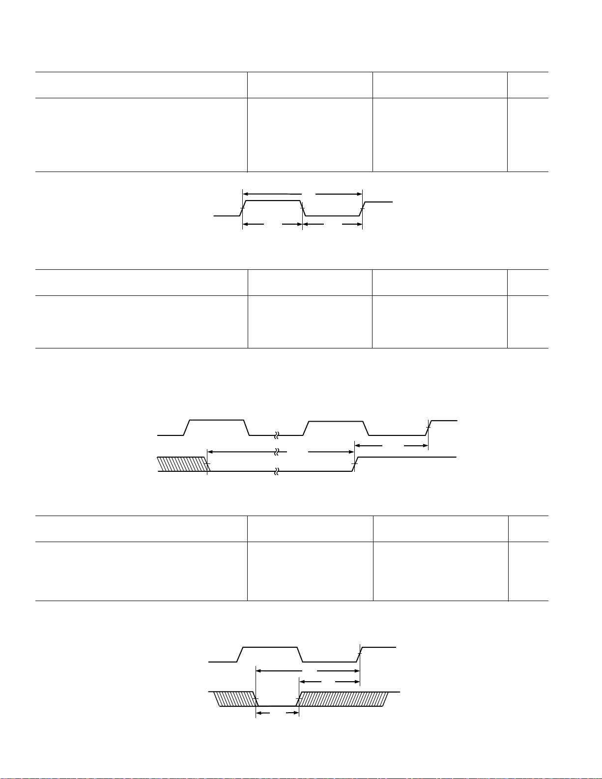
Memory Read—Bus Master
Use these specifications for asynchronous interfacing to memories (and memory-mapped peripherals) without reference to
CLKIN. These specifications apply when the AD14160/
These switching characteristics also apply for bus master synchronous read/write timing (see Synchronous Read/Write—Bus
Master below). If these timing requirements are met, the synchronous read/write timing can be ignored (and vice versa).
AD14160L is the bus master accessing external memory space.
40 MHz–5 V 40 MHz–3.3 V
Parameter Min Max Min Max Units
Timing Requirements:
t
DAD
t
DRLD
t
HDA
t
HDRH
t
DAAK
t
DSAK
Address, Selects Delay to Data Valid
RD Low to Data Valid
Data Hold from Address
Data Hold from RD High
ACK Delay from Address
ACK Delay from RD Low
1
3
3
2, 4
4
1, 2
17 + DT + W 17 + DT + W ns
11 + 5DT/8 + W 11 + 5DT/8 + W ns
1.5 1.5 ns
33ns
13 + 7DT/8 + W 13 + 7DT/8 + W ns
7 + DT/2 + W 7 + DT/2 + W ns
Switching Characteristics:
t
DRHA
t
DARL
t
RW
t
RWR
t
SADADC
W = (number of wait states specified in WAIT register) × t
HI = tCK (if an address hold cycle or bus idle cycle occurs, as specified in WAIT register; otherwise HI = 0).
H = tCK (if an address hold cycle occurs as specified in WAIT register; otherwise H = 0).
NOTES
1
Data Delay/Setup: User must meet t
2
For MSx, SW, BMS, the falling edge is referenced.
3
Data Hold: User must meet t
given capacitive and dc loads.
4
ACK Delay/Setup: User must meet t
Address Hold After RD High –1 + H –1 + H ns
Address to RD Low
2
1 + 3DT/8 1 + 3DT/8 ns
RD Pulsewidth 12.5 + 5DT/8 + W 12.5 + 5DT/8 + W ns
RD High to WR, RD, DMAGx Low 7.5 + 3DT/8 + HI 7.5 + 3DT/8 + HI ns
Address Setup Before ADRCLK High2–0.5 + DT/4 –0.5 + DT/4 ns
CK.
or t
HDA
DAD
DRLD
or t
or synchronous spec t
HDRH
or t
DSAK
or synchronous spec t
HDATI
or synchronous specification t
DAAK
.
SSDATI
. See System Hold Time Calculation under Test Conditions for the calculation of hold times
.
SACKC
ADDRESS
MSx, SW
BMS
RD
DATA
ACK
WR, DMAG
ADRCLK
(OUT)
t
SADADC
t
DARL
t
t
RW
t
DRLD
DAD
DAAK
t
t
DSAK
Figure 14. Memory Read—Bus Master
t
t
HDRH
t
HDA
DRHA
t
RWR
–18–
REV. A

AD14160/AD14160L
Memory Write—Bus Master
Use these specifications for asynchronous interfacing to memories (and memory-mapped peripherals) without reference to
CLKIN. These specifications apply when the AD14160/
These switching characteristics also apply for bus master synchronous read/write timing (see Synchronous Read/Write—Bus
Master). If these timing requirements are met, the synchronous
read/write timing can be ignored (and vice versa).
AD14160L is the bus master accessing external memory space.
40 MHz–5 V 40 MHz–3.3 V
Parameter Min Max Min Max Units
Timing Requirements:
t
DAAK
t
DSAK
ACK Delay from Address, Selects
ACK Delay from WR Low
1, 2
1
13 + 7DT/8 + W 13 + 7DT/8 + W ns
7 + DT/2 + W 7 + DT/2 + W ns
Switching Characteristics:
t
DAWH
t
DAWL
t
WW
t
DDWH
t
DWHA
t
DATRWH
t
WWR
t
DDWR
t
WDE
t
SADADC
W = (number of wait states specified in WAIT register) × tCK.
H = tCK (if an address hold cycle occurs, as specified in WAIT register; otherwise H = 0).
I = tCK (if a bus idle cycle occurs, as specified in WAIT register; otherwise I = 0).
NOTES
1
ACK Delay/Setup: User must meet t
2
For MSx, SW, BMS, the falling edge is referenced.
3
See System Hold Time Calculation under Test Conditions for calculation of hold times given capacitive and dc loads.
Address, Selects to WR Deasserted216 + 15DT/16 + W 16 + 15DT/16 + W ns
Address, Selects to WR Low
2
2 + 3DT/8 2 + 3DT/8 ns
WR Pulsewidth 12 + 9DT/16 + W 12 + 9DT/16 + W ns
Data Setup Before WR High 6 + DT/2 + W 6 + DT/2 + W ns
Address Hold After WR Deasserted 0 + DT/16 + H 0 + DT/16 + H ns
Data Disable After WR Deasserted30.5 + DT/16 + H 7 + DT/16 + H 0.5 + DT/16 + H 7 + DT/16 + H ns
WR High to WR, RD, DMAGx Low 7.5 + 7DT/16 + H 7.5 + 7DT/16 + H ns
Data Disable Before WR or RD Low 4 + 3DT/8 + I 4 + 3DT/8 + I ns
WR Low to Data Enabled –1.5 + DT/16 –1.5 + DT/16 ns
Address, Selects to ADRCLK High2–0.5 + DT/4 –0.5 + DT/4 ns
or t
DAAK
or synchronous specification t
DSAK
SACKC
.
ADDRESS
MSx , SW
BMS
WR
DATA
ACK
RD , DMAG
ADRCLK
(OUT)
t
SADADC
t
DAWL
t
DAWH
t
WW
t
WDE
t
DSAK
t
DAAK
Figure 15. Memory Write—Bus Master
t
DDWH
t
DATRWH
t
DWHA
t
WWR
t
DDWR
REV. A
–19–

AD14160/AD14160L
Synchronous Read/Write—Bus Master
Use these specifications for interfacing to external memory
systems that require CLKIN—relative timing or for accessing a
slave ADSP-2106x (in multiprocessor memory space). These
synchronous switching characteristics are also valid during asyn-
When accessing a slave ADSP-2106x, these switching characteristics must meet the slave’s timing requirements for synchronous
read/writes (see Synchronous Read/Write—Bus Slave). The
slave ADSP-2106x must also meet these (bus master) timing
requirements for data and acknowledge setup and hold times.
chronous memory reads and writes (see Memory Read—Bus
Master and Memory Write—Bus Master).
40 MHz–5 V 40 MHz–3.3 V
Parameter Min Max Min Max Units
Timing Requirements:
t
SSDATI
t
HSDATI
t
DAAK
t
SACKC
t
HACKC
Data Setup Before CLKIN 3.5 + DT/8 3.5 + DT/8 ns
Data Hold After CLKIN 3.5 – DT/8 3.5 – DT/8 ns
ACK Delay After Address,
MSx, SW, BMS
ACK Setup Before CLKIN
1, 2
2
7 + DT/4 7 + DT/4 ns
13 + 7 DT/8 + W 13 + 7 DT/8 + W ns
ACK Hold After CLKIN –1 – DT/4 –1 – DT/4 ns
Switching Characteristics:
t
DADRO
t
HADRO
Address, MSx, BMS, SW Delay
After CLKIN
1
Address, MSx, BMS, SW Hold
8 – DT/8 8 – DT/8 ns
After CLKIN –1 – DT/8 –1 – DT/8 ns
t
DPGC
t
DRDO
t
DWRO
t
DRWL
t
SDDATO
t
DATTR
t
DADCCK
t
ADRCK
t
ADRCKH
t
ADRCKL
W = (number of Wait states specified in WAIT register) × tCK.
NOTES
1
For MSx, SW, BMS, the falling edge is referenced.
2
ACK Delay/Setup: User must meet t
3
See System Hold Time Calculation under Test Conditions for calculation of hold times given capacitive and dc loads.
PAGE Delay After CLKIN 9 + DT/8 16.5 + DT/8 9 + DT/8 16.5 + DT/8 ns
RD High Delay After CLKIN –2 – DT/8 5 – DT/8 –2 – DT/8 5 – DT/8 ns
WR High Delay After CLKIN –3 – 3DT/16 5 – 3DT/16 –3 – 3DT/16 5 – 3DT/16 ns
RD/WR Low Delay After CLKIN 8 + DT/4 13.5 + DT/4 8 + DT/4 13.5 + DT/4 ns
Data Delay After CLKIN 20 + 5DT/16 20 + 5DT/16 ns
Data Disable After CLKIN
3
0 – DT/8 8 – DT/8 0 – DT/8 8 – DT/8 ns
ADRCLK Delay After CLKIN 4 + DT/8 10.5 + DT/8 4 + DT/8 10.5 + DT/8 ns
ADRCLK Period t
CK
t
CK
ns
ADRCLK Width High (tCK/2 – 2) (tCK/2 – 2) ns
ADRCLK Width Low (tCK/2 – 2) (tCK/2 – 2) ns
or t
DAAK
or synchronous specification t
DSAK
SACKC
.
–20–
REV. A

CLKIN
ADRCLK
ADDRESS
SW
PAGE
ACK
(IN)
READ CYCLE
RD
DATA
(IN)
t
DADRO
t
DADCCK
t
t
DPGC
DRWL
t
DAAK
t
ADRCKH
t
ADRCK
t
SACKC
t
SSDATI
AD14160/AD14160L
t
ADRCKL
t
HADRO
t
HACKC
t
DRDO
t
HSDATI
WRITE CYCLE
WR
DATA
(OUT)
t
DRWL
t
SDDATO
Figure 16. Synchronous Read/Write—Bus Master
t
DWRO
t
DATTR
REV. A
–21–

AD14160/AD14160L
Synchronous Read/Write—Bus Slave
The bus master must meet these (bus slave) timing requirements.
Use these specifications for bus master accesses of a slave’s IOP
registers or internal memory (in multiprocessor memory space).
40 MHz–5 V 40 MHz–3.3 V
Parameter Min Max Min Max Units
Timing Requirements:
t
SADRI
t
HADRI
t
SRWLI
t
HRWLI
t
RWHPI
t
SDATWH
t
HDATWH
Address, SW Setup Before CLKIN 15.5 + DT/2 15.5 + DT/2 ns
Address, SW Hold Before CLKIN 5 + DT/2 5 + DT/2 ns
RD/WR Low Setup Before CLKIN110 + 5DT/16 10 + 5DT/16 ns
RD/WR Low Hold After CLKIN –4 – 5DT/16 7.5 + 7DT/16 –4 – 5DT/16 7.5 + 7DT/16 ns
RD/WR Pulse High 3 3 ns
Data Setup Before WR High 6 6 ns
Data Hold After WR High 1.5 1.5 ns
Switching Characteristics:
t
SDDATO
t
DATTR
t
DACKAD
t
ACKTR
NOTES
1
t
(min) = 10 + 5DT/16 when Multiprocessor Memory Space Wait State (MMSWS bit in WAIT register) is disabled; when MMSWS is enabled,
SRWLI
t
(min) = 4.5 + DT/8.
SRWLI
2
See System Hold Time Calculation under Test Conditions for calculation of hold times given capacitive and dc loads.
3
t
is true only if the address and SW inputs have setup times (before CLKIN) greater than 10.5 + DT/8 and less than 19 + 3DT/4. If the address and SW inputs have
DACKAD
setup times greater than 19 + 3DT/4, then ACK is valid 15 + DT/4 (max) after CLKIN. A slave that sees an address with an M field match will respond with ACK
regardless of the state of MMSWS or strobes. A slave will three-state ACK every cycle with t
Data Delay After CLKIN 20 + 5DT/16 20 + 5DT/16 ns
Data Disable After CLKIN
ACK Delay After Address, SW
ACK Disable After CLKIN
2
3
3
0 – DT/8 8 – DT/8 0 – DT/8 8 – DT/8 ns
10 10 ns
–1 – DT/8 7 – DT/8 –1 – DT/8 7 – DT/8 ns
.
ACKTR
CLKIN
ADDRESS
SW
ACK
READ ACCESS
RD
DATA
(OUT)
WRITE ACCESS
WR
DATA
(IN)
t
t
SDDATO
t
DACKAD
SADRI
t
SRWLI
t
SRWLI
t
HADRI
t
SDATWH
Figure 17. Synchronous Read/Write—Bus Slave
t
HRWLI
t
HRWLI
t
HDATWH
t
t
DATTR
ACKTR
t
RWHPI
t
RWHPI
–22–
REV. A

AD14160/AD14160L
Multiprocessor Bus Request and Host Bus Request
Use these specifications for passing of bus mastership between
multiprocessing ADSP-2106x’s (BRx) or a host processor
(HBR, HBG).
40 MHz–5 V 40 MHz–3.3 V
Parameter Min Max Min Max Units
Timing Requirements:
t
HBGRCSV
t
SHBRI
t
HHBRI
t
SHBGI
t
HHBGI
t
SBRI
t
HBRI
t
SRPBAI
t
HRPBAI
HBG Low to RD/WR/CS Valid
HBR Setup Before CLKIN
HBR Hold Before CLKIN
HBG Setup Before CLKIN 13 + DT/2 13 + DT/2 ns
HBG Hold Before CLKIN High 6 + DT/2 6 + DT/2 ns
BRx, CPA Setup Before CLKIN
BRx, CPA Hold Before CLKIN High 6 + DT/2 6 + DT/2 ns
RPBA Setup Before CLKIN 21.5 + 3DT/4 21.5 + 3DT/4 ns
RPBA Hold Before CLKIN 12 + 3DT/4 12 + 3DT/4 ns
Switching Characteristics:
t
DHBGO
t
HHBGO
t
DBRO
t
HBRO
t
DCPAO
t
TRCPA
t
DRDYCS
HBG Delay After CLKIN 7.5 – DT/8 7.5 – DT/8 ns
HBG Hold After CLKIN –2 – DT/8 –2 – DT/8 ns
BRx Delay After CLKIN 8 – DT/8 8 – DT/8 ns
BRx Hold After CLKIN –2 – DT/8 –2 – DT/8 ns
CPA Low Delay After CLKIN 8.5 – DT/8 8.5 – DT/8 ns
CPA Disable After CLKIN –2 – DT/8 5 – DT/8 –2 – DT/8 5 – DT/8 ns
REDY (O/D) or (A/D) Low from CS
and HBR Low
t
TRDYHG
REDY (O/D) Disable or REDY (A/D)
High from HBG
t
ARDYTR
REDY (A/D) Disable from CS or HBR
4
High
4
4
1
2
2
3
20 + 3DT/4 20 + 3DT/4 ns
13.5 + DT/2 13.5 + DT/2 ns
19.5 + 5DT/4 19.5 + 5DT/4 ns
14 + 3DT/4 14 + 3DT/4 ns
9.5 10.25 ns
43.5 + 27DT/16 43.5 + 27DT/16 ns
11 11 ns
NOTES
1
For first asynchronous access after HBR and CS asserted, ADDR
low. This is easily accomplished by driving an upper address signal high when HBG is asserted.
2
Only required for recognition in the current cycle.
3
CPA assertion must meet the setup to CLKIN; deassertion does not need to meet the setup to CLKIN.
4
(O/D) = open drain, (A/D) = active drive.
must be a non-MMS value 1/2 tCK before RD or WR goes low or by t
31–0
HBGRCSV
after HBG goes
REV. A
–23–

AD14160/AD14160L
CLKIN
HBR
HBG
(OUT)
BRx
(OUT)
CPA (OUT)
(O/D)
HBG (IN)
BRx (IN)
CPA (IN)
(O/D)
HBR
CS
t
DRDYCS
REDY (O/D)
REDY (A/D)
t
SHBRI
t
HHBRI
t
HHBGO
t
HBRO
t
t
t
DBRO
DHBGO
DCPAO
t
TRDYHG
t
t
SHBGI
SBRI
t
t
HHBGI
HBRI
t
TRCPA
t
ARDYTR
HBG (OUT)
RD
WR
CS
RPBA
t
SRPBAI
O/D = OPEN DRAIN, A/D = ACTIVE DRIVE
NOTE:
HBG WILL BE DELAYED BY n CLOCK CYCLES
WHEN WAIT STATES OR BUS LOCK ARE IN EFFECT.
t
HRPBAI
Figure 18. Multiprocessor Bus Request and Host Bus Request
t
HBGRCSV
–24–
REV. A

AD14160/AD14160L
Asynchronous Read/Write—Host to AD14160/AD14160L
Use these specifications for asynchronous host processor accesses
of an AD14160/AD14160L, after the host has asserted CS and
the host can drive the RD and WR pins to access the AD14160/
AD14160L’s internal memory or IOP registers. HBR and HBG
are assumed low for this timing.
HBR (low). After HBG is returned by the AD14160/AD14160L,
40 MHz–5 V 40 MHz–3.3 V
Parameter Min Max Min Max Units
Lead Cycle
Timing Requirements:
t
SADRDL
t
HADRDH
t
WRWH
t
DRDHRDY
t
DRDHRDY
Address Setup/CS Low Before RD Low
Address Hold/CS Hold Low After RD 11 ns
RD/WR High Width 6 6 ns
RD High Delay After REDY (O/D) Disable 0.5 0.5 ns
RD High Delay After REDY (A/D) Disable 0.5 0.5 ns
1
11 ns
Switching Characteristics:
t
SDATRDY
t
DRDYRDL
t
RDYPRD
t
HDARWH
Data Valid Before REDY Disable from Low 1 1 ns
REDY (O/D) or (A/D) Low Delay After RD Low 11 11.5 ns
REDY (O/D) or (A/D) Low Pulsewidth for Read 45 + DT 45 + DT ns
Data Disable After RD High 2 9.5 2 10 ns
Write Cycle
Timing Requirements:
t
SCSWRL
t
HCSWRH
t
SADWRH
t
HADWRH
t
WWRL
t
WRWH
t
DWRHRDY
t
SDATWH
t
HDATWH
CS Low Setup Before WR Low 0 0 ns
CS Low Hold After WR High 0.5 0.5 ns
Address Setup Before WR High 6 6 ns
Address Hold After WR High 2.5 2.5 ns
WR Low Width 7 7 ns
RD/WR High Width 6 6 ns
WR High Delay After REDY (O/D) or (A/D) Disable 0.5 0.5 ns
Data Setup Before WR High 6 6 ns
Data Hold After WR High 1.5 1.5 ns
Switching Characteristics:
t
DRDYWRL
t
RDYPWR
t
SRDYCK
NOTE
1
Not required if RD and address are valid t
or WR goes low or by t
driven during asynchronous host accesses, see Table 8.2 of the ADSP-2106x SHARC User’s Manual.
REDY (O/D) or (A/D) Low Delay After WR/CS Low 11 11.5 ns
REDY (O/D) or (A/D) Low Pulsewidth for Write 15 15 ns
REDY (O/D) or (A/D) Disable to CLKIN 0.5 + 7DT/16 8 + 7DT/16 0.5 + 7DT/16 8 + 7DT/16 ns
after HBG goes low. For first access after HBR asserted, ADDR
after HBG goes low. This is easily accomplished by driving an upper address signal high when HBG is asserted. For address bits to be
HBGRCSV
HBGRCSV
CLKIN
REDY (O/D)
REDY (A/D)
O/D = OPEN DRAIN, A/D = ACTIVE DRIVE
Figure 19a. Synchronous REDY Timing
t
SRDYCK
must be a non-MMS value 1/2 t
31–0
before RD
CLK
REV. A
–25–

AD14160/AD14160L
READ CYCLE
ADDRESS/CS
RD
DATA (OUT)
REDY (O/D)
REDY (A/D)
WRITE CYCLE
ADDRESS
CS
WR
DATA (IN)
REDY (O/D)
t
SADRDL
t
SCSWRL
t
DRDYRDL
t
DRDYWRL
t
t
t
WWRL
t
SDATRDY
RDYPRD
RDYPWR
t
t
SDATWH
t
DRDHRDY
SADWRH
t
t
DWRHRDY
HCSWRH
t
HDARWH
t
HADWRH
t
HDATWH
t
HADRDH
t
WRWH
t
WRWH
REDY (A/D)
O/D = OPEN DRAIN, A/D = ACTIVE DRIVE
Figure 19b. Asynchronous Read/Write—Host to ADSP-2106x
–26–
REV. A

AD14160/AD14160L
Three-State Timing—Bus Master, Bus Slave, HBR, SBTS
These specifications show how the memory interface is disabled
(stops driving) or enabled (resumes driving) relative to CLKIN
and the SBTS pin. This timing is applicable to bus master transition cycles (BTC) and host transition cycles (HTC) as well as
the SBTS pin.
40 MHz–5 V 40 MHz–3.3 V
Parameter Min Max Min Max Units
Timing Requirements:
t
STSCK
t
HTSCK
Switching Characteristics:
t
MIENA
t
MIENS
t
MIENHG
t
MITRA
t
MITRS
t
MITRHG
t
DATEN
t
DATTR
t
ACKEN
t
ACKTR
t
ADCEN
t
ADCTR
t
MTRHBG
t
MENHBG
SBTS Setup Before CLKIN 12 + DT/2 12 + DT/2 ns
SBTS Hold Before CLKIN 6 + DT/2 6 + DT/2 ns
Address/Select Enable After CLKIN –1.5 – DT/8 –1.25 – DT/8 ns
Strobes Enable After CLKIN
1
–1.5 – DT/8 –1.5 – DT/8 ns
HBG Enable After CLKIN –1.5 – DT/8 –1.5 – DT/8 ns
Address/Select Disable After CLKIN 1 – DT/4 1 – DT/4 ns
Strobes Disable After CLKIN
HBG Disable After CLKIN 2.5 – DT/4 2.5 – DT/4 ns
Data Enable After CLKIN
Data Disable After CLKIN
ACK Enable After CLKIN
ACK Disable After CLKIN
1
2
2
2
2
9 + 5DT/16 9 + 5DT/16 ns
0 – DT/8 8 – DT/8 0 – DT/8 8 – DT/8 ns
7.5 + DT/4 7.5 + DT/4 ns
–1 – DT/8 7 – DT/8 –1 – DT/8 7 – DT/8 ns
2.5 – DT/4 2.5 – DT/4 ns
ADRCLK Enable After CLKIN –2 – DT/8 –2 – DT/8 ns
ADRCLK Disable After CLKIN 8.5 – DT/4 8.5 – DT/4 ns
Memory Interface Disable Before HBG Low3–0.5 + DT/8 –0.5 + DT/8 ns
Memory Interface Enable After HBG High318.5 + DT 18.5 + DT ns
NOTES
1
Strobes = RD, WR, SW, PAGE, DMAG.
2
In addition to bus master transition cycles, these specs also apply to bus master and bus slave synchronous read/write.
3
Memory Interface = Address, RD, WR, MSx, SW, HBG, PAGE, DMAGx, BMS (in EPROM boot mode).
CLKIN
t
SBTS
MEMORY
INTERFACE
DATA
ACK
ADRCLK
HBG
MEMORY
INTERFACE
STSCK
t
MIENA, tMIENS, tMIENHG
t
DATEN
t
ACKEN
t
ADCEN
t
MENHBG
MEMORY INTERFACE = ADDRESS, RD, WR, MSx, SW, HBG, PAGE, DMAGx. BMS (IN EPROM BOOT MODE)
t
HTSCK
t
MITRA, tMITRS, tMITRHG
t
DATTR
t
ACKTR
t
ADCTR
Figure 20. Three-State Timing
t
MTRHBG
REV. A
–27–

AD14160/AD14160L
DMA Handshake
These specifications describe the three DMA handshake modes.
In all three modes DMAR is used to initiate transfers. For handshake mode, DMAG controls the latching or enabling of data
externally. For external handshake mode, the data transfer is
controlled by the ADDR
, RD, WR, SW, PAGE, MS
31-0
3-0
,
transfer is controlled by ADDR
(not DMAG). For Paced Master mode, the “Memory Read–Bus
Master”, “Memory Write–Bus Master”, and “Synchronous
Read/Write–Bus Master” timing specifications for ADDR
RD, WR, MS
, SW, PAGE, DATA
3-0
, RD, WR, MS
31-0
, and ACK also apply.
47-0
, and ACK
3-0
31-0
,
ACK, and DMAG signals. For Paced Master mode, the data
40 MHz–5 V 40 MHz–3.3 V
Parameter Min Max Min Max Units
Timing Requirements:
t
SDRLC
t
SDRHC
t
WDR
t
SDATDGL
t
HDATIDG
t
DATDRH
t
DMARLL
t
DMARH
DMARx Low Setup Before CLKIN
DMARx High Setup Before CLKIN
DMARx Width Low (Nonsynchronous) 6 6 ns
Data Setup After DMAGx Low
Data Hold After DMAGx High 2.5 2.5 ns
Data Valid After DMAGx High
DMAGx Low Edge to Low Edge 23 + 7DT/8 23 + 7DT/8 ns
DMAGx Width High 6 6 ns
1
1
2
2
5.5 5.5 ns
5.5 5.5 ns
9 + 5DT/8 9 + 5DT/8 ns
15 + 7DT/8 15 + 7DT/8 ns
Switching Characteristics:
t
DDGL
t
WDGH
t
WDGL
t
HDGC
t
VDATDGH
t
DATRDGH
t
DGWRF
t
DGWRH
t
DGWRR
t
DGRDF
t
DRDGH
t
DGRDR
t
DGWR
t
DADGH
t
DDGHA
W = (number of wait states specified in WAIT register) × tCK.
HI = tCK (if an address hold cycle or bus idle cycle occurs, as specified in WAIT register; otherwise HI = 0).
NOTES
1
Only required for recognition in the current cycle.
2
t
SDATDGL
data can be driven t
3
t
VDATDGH
n equals the number of extra cycles that the access is prolonged.
4
See System Hold Time Calculation under Test Conditions for calculation of hold times given capacitive and dc loads.
DMAGx Low Delay After CLKIN 9 + DT/4 16 + DT/4 9 + DT/4 16 + DT/4 ns
DMAGx High Width 6 + 3DT/8 6 + 3DT/8 ns
DMAGx Low Width 12 + 5DT/8 12 + 5DT/8 ns
DMAGx High Delay After CLKIN –2 – DT/8 7 – DT/8 –2 – DT/8 7 – DT/8 ns
Data Valid Before DMAGx High
Data Disable After DMAGx High
3
4
7 + 9DT/16 7 + 9DT/16 ns
–0.5 8 –0.5 8 ns
WR Low Before DMAGx Low –0.5 2.5 –0.5 2.5 ns
DMAGx Low Before WR High 9.5 + 5DT/8 + W 9.5 + 5DT/8 + W ns
WR High Before DMAGx High 0.5 + DT/16 3.5 + DT/16 0.5 + DT/16 3.5 + DT/16 ns
RD Low Before DMAGx Low –0.5 2.5 –0.5 2.5 ns
RD Low Before DMAGx High 10.5 + 9DT/16 + W 10.5 + 9DT/16 + W ns
RD High Before DMAGx High –0.5 3.5 –0.5 3.5 ns
DMAGx High to WR, RD, DMAGx Low 5 + 3DT/8 + HI 5 + 3DT/8 + HI ns
Address/Select Valid to DMAGx High 16 + DT 16 + DT ns
Address/Select Hold After DMAGx High –1.5 –1.5 ns
is the data setup requirement if DMARx is not being used to hold off completion of a write. Otherwise, if DMARx low holds off completion of the write, the
is valid if DMARx is not being used to hold off completion of a read. If DMARx is used to prolong the read, then t
after DMARx is brought high.
DATDRH
= 7 + 9DT/16 + (n × tCK) where
VDATDGH
–28–
REV. A

CLKIN
DMARx
DMAGx
t
SDRLC
AD14160/AD14160L
t
DMARLL
t
WDR
t
DDGL
t
t
WDGL
SDRHC
t
DMARH
t
HDGC
t
WDGH
TRANSFERS BETWEEN ADSP-2106x INTERNAL MEMORY AND EXTERNAL DEVICE
DATA (FROM
ADSP-2106x TO
EXTERNAL DRIVE)
t
DATDRH
t
DATA (FROM
EXTERNAL DRIVE
TO ADSP-2106x)
SDATDGL
TRANSFERS BETWEEN EXTERNAL DEVICE AND EXTERNAL MEMORY* (EXTERNAL HANDSHAKE MODE)
t
WR
(EXTERNAL DEVICE
TO EXTERNAL
MEMORY)
RD
(EXTERNAL
MEMORY TO
EXTERNAL DEVICE)
ADDRESS
MS
, SW
X
*
“MEMORY READ – BUS MASTER,” “MEMORY WRITE – BUS MASTER,” AND “SYNCHRONOUS READ/WRITE – BUS MASTER”
TIMING SPECIFICATIONS FOR ADDR
, RD, WR, SW, MS
31–0
DGWRL
t
DGRDL
AND ACK ALSO APPLY HERE.
3-0
t
DGWRH
t
DADGH
t
DRDGH
Figure 21. DMA Handshake Timing
t
VDATDGH
t
DGWRR
t
DGRDR
t
DATRDGH
t
HDATIDG
t
DDGHA
REV. A
–29–

AD14160/AD14160L
Link Ports: 1 × CLK Speed Operation
40 MHz–5 V 40 MHz–3.3 V
Parameter Min Max Min Max Units
Receive
Timing Requirements:
t
SLDCL
t
HLDCL
t
LCLKIW
t
LCLKRWL
t
LCLKRWH
Switching Characteristics:
t
DLAHC
t
DLALC
t
ENDLK
t
TDLK
Transmit
Timing Requirements:
t
SLACH
t
HLACH
Switching Characteristics:
t
DLCLK
t
DLDCH
t
HLDCH
t
LCLKTWL
t
LCLKTWH
t
DLACLK
t
ENDLK
t
TDLK
Data Setup Before LCLK Low 3.5 3 ns
Data Hold After LCLK Low 3 3 ns
LCLK Period (1 × Operation) t
CK
t
CK
ns
LCLK Width Low 6 6 ns
LCLK Width High 5 5 ns
LACK High Delay After CLKIN High 18 + DT/2 29 + DT/2 18 + DT/2 29 + DT/2 ns
LACK Low Delay After LCLK High
1
–3 13.5 –3 13.5 ns
LACK Enable from CLKIN 5 + DT/2 5 + DT/2 ns
LACK Disable from CLKIN 20.5 + DT/2 20.5 + DT/2 ns
LACK Setup Before LCLK High 18 20 ns
LACK Hold After LCLK High –7 –7 ns
LCLK Delay After CLKIN (1 × Operation) 16 17 ns
Data Delay After LCLK High 3.5 3 ns
Data Hold After LCLK High –3 –3 ns
LCLK Width Low (tCK/2) – 2 (tCK/2) + 2 (tCK/2) – 1 (tCK/2) + 1.25 ns
LCLK Width High (tCK/2) – 2 (tCK/2) + 2 (tCK/2) – 1.25 (tCK/2) + 1 ns
LCLK Low Delay After LACK High (tCK/2) + 8.5 (3 × tCK/2) + 17.5 (tCK/2) + 8 (3 × tCK/2) + 18 ns
LDAT, LCLK Enable After CLKIN 5 + DT/2 5 + DT/2 ns
LDAT, LCLK Disable After CLKIN 20.5 + DT/2 20.5 + DT/2 ns
Link Port Service Request Interrupts: 1 × and
2 × Speed Operations
Timing Requirements:
t
SLCK
t
HLCK
NOTES
1
LACK will go low with t
2
Only required for interrupt recognition in the current cycle.
LACK/LCLK Setup Before CLKIN Low210 10 ns
LACK/LCLK Hold After CLKIN Low
relative to rising edge of LCLK after first nibble is received. LACK will not go low if the receiver’s link buffer is not about to fill.
DLALC
2
22ns
–30–
REV. A

AD14160/AD14160L
Link Ports: 2 × CLK Speed Operation
40 MHz–5 V 40 MHz–3.3 V
Parameter Min Max Min Max Units
Receive
Timing Requirements:
t
SLDCL
t
HLDCL
t
LCLKIW
t
LCLKRWL
t
LCLKRWH
Switching Characteristics:
t
DLAHC
t
DLALC
Transmit
Timing Requirements:
t
SLACH
t
HLACH
Switching Characteristics:
t
DLCLK
t
DLDCH
t
HLDCH
t
LCLKTWL
t
LCLKTWH
t
DLACLK
Data Setup Before LCLK Low 2.5 2.25 ns
Data Hold After LCLK Low 2.25 2.25 ns
LCLK Period (2 × Operation) tCK/2 tCK/2 ns
LCLK Width Low 4.5 5 ns
LCLK Width High 4.25 4 ns
LACK High Delay After CLKIN High 18 + DT/2 29 + DT/2 18 + DT/2 30 + DT/2 ns
LACK Low Delay After LCLK High16 16.5 6 18.5 ns
LACK Setup Before LCLK High 19 19 ns
LACK Hold After LCLK High –6.75 –6.5 ns
LCLK Delay After CLKIN 8.5 8.5 ns
Data Delay After LCLK High 3 2.75 ns
Data Hold After LCLK High –2 –2 ns
LCLK Width Low (tCK/4) – 1 (tCK/4) + 1 (tCK/4) – 0.75 (tCK/4) + 1.5 ns
LCLK Width High (tCK/4) – 1 (tCK/4) + 1 (tCK/4) – 1.5 (tCK/4) + 1 ns
LCLK Low Delay After LACK High (tCK/4) + 9 (3 × tCL/4) + 17 (tCK/4) + 9 (3 × tCL/4) + 17 ns
NOTE
1
LACK will go low with t
relative to rising edge of LCLK after first nibble is received. LACK will not go low if the receiver’s link buffer is not about to fill.
DLALC
REV. A
–31–

AD14160/AD14160L
TRANSMIT
CLKIN
t
DLCLK
t
LCLKTWH
LCLK 1x
OR
LCLK 2x
t
HLDCH
t
DLDCH
t
LCLKTWL
LAST NIBBLE
TRANSMITTED
FIRST NIBBLE
TRANSMITTED
LCLK INACTIVE
(HIGH)
LDAT(3:0)
LACK (IN)
THE
OUT
t
SLACH
t
REQUIREMENT APPLIES TO THE RISING EDGE OF LCLK ONLY FOR THE FIRST NIBBLE TRANSMITTED.
SLACH
RECEIVE
CLKIN
t
LCLKIW
t
HLDCL
IN
t
LCLKRWL
LCLK 1x
OR
LCLK 2x
LDAT(3:0)
LACK (OUT)
t
LCLKRWH
t
SLDCL
t
DLAHC
LACK GOES LOW ONLY AFFTER THE SECOND NIBBLE IS RECEIVED.
LINK PORT ENABLE/THREE-STATE DELAY FROM INSTRUCTION
CLKIN
LCLK
LDAT(3:0)
LACK
t
ENDLK
LINK PORT ENABLE OR THREE-STATE TAKES EFFECT 2 CYCLES AFTER A WRITE TO A LINK PORT CONTROL REGISTER.
t
TDLK
t
HLACH
t
DLALC
t
DLACLK
LINK PORT INTERRUPT SETUP TIME
CLKIN
t
SLCK
LCLK
LACK
t
HLCK
Figure 22. Link Ports
–32–
REV. A

AD14160/AD14160L
Serial Ports
40 MHz–5 V 40 MHz–3.3 V
Parameter Min Max Min Max Units
External Clock
Timing Requirements:
t
SFSE
t
HFSE
t
SDRE
t
HDRE
t
SCLKW
t
SCLK
TFS/RFS Setup Before TCLK/RCLK
TFS/RFS Hold After TCLK/RCLK
Receive Data Setup Before RCLK
Receive Data Hold After RCLK
TCLK/RCLK Width 9.5 9 ns
TCLK/RCLK Period t
Internal Clock
Timing Requirements:
t
SFSI
t
HFSI
t
SDRI
t
HDRI
TFS Setup Before TCLK1; RFS Setup Before RCLK188 ns
TFS/RFS Hold After TCLK/RCLK
Receive Data Setup Before RCLK
Receive Data Hold After RCLK
External or Internal Clock
Switching Characteristics:
t
DFSE
t
HFSE
RFS Delay After RCLK (Internally Generated RFS)
RFS Hold After RCLK (Internally Generated RFS)333 ns
External Clock
Switching Characteristics:
t
DFSE
t
HFSE
t
DDTE
t
HDTE
TFS Delay After TCLK (Internally Generated TFS)
TFS Hold After TCLK (Internally Generated TFS)333 ns
Transmit Data Delay After TCLK
Transmit Data Hold After TCLK
Internal Clock
Switching Characteristics:
t
DFSI
t
HFSI
t
DDTI
t
HDTI
t
SCLKIW
TFS Delay After TCLK (Internally Generated TFS)
TFS Hold After TCLK (Internally Generated TFS)3–1.5 –1.5 ns
Transmit Data Delay After TCLK
Transmit Data Hold After TCLK
TCLK/RCLK Width (SCLK/2) – 2 (SCLK/2) + 2 (SCLK/2) – 2.5 (SCLK/2) + 2.5 ns
Enable and Three-State
Switching Characteristics:
t
DDTEN
t
DDTTE
t
DDTIN
t
DDTTI
t
DCLK
t
DPTR
Data Enable from External TCLK
Data Disable from External TCLK
Data Enable from Internal TCLK
Data Disable from Internal TCLK
TCLK/RCLK Delay from CLKIN 22.5 + 3DT/8 22.5 + 3DT/8 ns
SPORT Disable After CLKIN 17.5 17.5 ns
External Late Frame Sync
Switching Characteristics:
t
DDTLFSE
Data Delay from Late External TFS or 12.5 13.3 ns
External RFS with MCE = 1, MFD = 0
t
DDTENFS
Data Enable from Late FS or MCE = 1, MFD = 043 3.5 ns
1
1, 2
1
1
1, 2
1
1
3
3
3
3
3
3
3
3
4
3.5 3.5 ns
44 ns
1.5 1.5 ns
44 ns
CK
t
CK
ns
11 ns
33 ns
33 ns
3
3
13.5 13.5 ns
13.5 13.5 ns
16.5 16.5 ns
55 ns
3
4.5 4.5 ns
7.5 7.5 ns
00 ns
3.5 4 ns
11 11 ns
00 ns
33ns
To determine whether communication is possible between two devices at clock speed n, the following specifications must be confirmed: 1) frame sync delay and frame
sync setup and hold, 2) data delay and data setup and hold, and 3) SCLK width.
NOTES
1
Referenced to sample edge.
2
RFS hold after RCK when MCE = 1, MFD = 0 is 0 ns minimum from drive edge. TFS hold after TCK for late external TFS is 0 ns minimum from drive edge.
3
Referenced to drive edge.
4
MCE = 1, TFS enable and TFS valid follow t
REV. A
DDTLFSE
and t
DDTENFS
.
–33–

AD14160/AD14160L
EXTERNAL RFS with MCE = 1, MFD = 0
DRIVE SAMPLE
RCLK
t
SFSE/I
RFS
DT
t
DDTLFSE
t
DDTENFS
t
HDTE/I
1ST BIT 2ND BIT
LATE EXTERNAL TFS
DRIVE
t
HFSE/I
t
DDTE/I
(SEE NOTE 2)
TCLK
TFS
DT
t
HDTE/I
DRIVE
t
t
HFSE/I
DDTE/I
DRIVE SAMPLE
t
SFSE/I
t
DDTENFS
1ST BIT 2ND BIT
t
DDTLFSE
Figure 23. External Late Frame Sync
(SEE NOTE 2)
–34–
REV. A

AD14160/AD14160L
DATA RECEIVE– INTERNAL CLOCK
DRIVE
RCLK
RFS
DR
EDGE
t
HFSE
NOTE: EITHER THE RISING EDGE OR FALLING EDGE OF RCLK, TCLK CAN BE USED AS THE ACTIVE SAMPLING EDGE.
t
DFSE
t
SCLKIW
t
SFSI
t
SDRI
DATA TRANSMIT– INTERNAL CLOCK
DRIVE
TCLK
TFS
DT
EDGE
t
t
HFSI
HDTI
t
t
DFSI
DDTI
t
SCLKIW
t
SFSI
SAMPLE
EDGE
SAMPLE
EDGE
t
t
t
HFSI
HDRI
HFSI
DATA RECEIVE– EXTERNAL CLOCK
DRIVE
RCLK
RFS
DR
EDGE
t
HFSE
t
DFSE
t
SCLKW
t
SFSE
t
SDRE
DATA TRANSMIT– EXTERNAL CLOCK
DRIVE
TCLK
TFS
EDGE
t
HFSE
t
HDTE
DT
t
DFSE
t
DDTE
t
SCLKW
t
SFSE
SAMPLE
EDGE
SAMPLE
EDGE
t
HFSE
t
HDRE
t
HFSE
TCLK (EXT)
TCLK (INT)
CLKIN
TCLK, RCLK
TFS, RFS, DT
TCLK (INT)
RCLK (INT)
NOTE: EITHER THE RISING EDGE OR FALLING EDGE OF RCLK, TCLK CAN BE USED AS THE ACTIVE SAMPLING EDGE.
DRIVE
EDGE
t
DDTEN
DT
DRIVE
EDGE
t
DDTIN
DT
SPORT DISABLE DELAY
FROM INSTRUCTION
LOW TO HIGH ONLY
t
DCLK
t
DPTR
SPORT ENABLE AND
THREE-STATE
LATENCY
IS TWO CYCLES
TCLK / RCLK
TCLK / RCLK
CLKIN
TFS (EXT)
NOTE: APPLIES ONLY TO GATED SERIAL CLOCK MODE WITH
EXTERNAL TFS, AS USED IN THE SERIAL PORT SYSTEM I/O FOR
MESH MULTIPROCESSING.
DRIVE
EDGE
DRIVE
EDGE
t
DDTTI
t
DDTTE
t
STFSCK
Figure 24. Serial Ports
t
HTFSCK
REV. A
–35–

AD14160/AD14160L
JTAG Test Access Port and Emulation
40 MHz–5 V 40 MHz–3.3 V
Parameter Min Max Min Max Units
Timing Requirements:
t
TCK
t
STAP
t
HTAP
t
SSYS
t
HSYS
t
TRSTW
Switching Characteristics:
t
DTDO
t
DSYS
NOTES
1
System Inputs = DATA
TCLKy0, TCLKy1, RCLKy0, RCLKy1, TFSy0, TFSy1, RFSy0, RFSy1, LxDAT
2
System Outputs = DATA
DT1, TCLK0, TCLK1, RCLK0, RCLK1, TFS0, TFS1, RFS0, RFS1, LxDAT
TCK Period t
CK
t
CK
ns
TDI, TMS Setup Before TCK High 5.5 5.5 ns
TDI, TMS Hold After TCK High 6.5 6.5 ns
System Inputs Setup Before TCK Low188ns
System Inputs Hold After TCK Low
TRST Pulsewidth 4t
TDO Delay from TCK Low 13.5 13.5 ns
System Outputs Delay After TCK Low
47-0
47-0
, ADDR
, ADDR
, RD, WR, ACK, SBTS, SW, HBR, HBG, CS, DMAR1, DMAR2, BR
31-0
, MS
31-0
TCK
, RD, WR, ACK, PAGE, ADRCLK, SW, HBG, REDY, DMAG1, DMAG2, BR
3-0
1
18.5 19 ns
CK
2
, LxCLK, LxACK, EBOOT, LBOOT, BMS, CLKIN, RESET.
3-0
, LxCLK, LxACK, BMS.
3-0
t
TCK
20 20 ns
4t
CK
, RPBA, IDy2-0, IRQ
6-1
, FLAGy3-0, DRy0, DyR1,
2-0
, CPA, FLAG
6-1
ns
, TIMEXP, DT0,
2-0
TMS
TDI
TDO
SYSTEM
INPUTS
SYSTEM
OUTPUTS
t
DTDO
t
t
STAP
DSYS
t
HTAP
t
SSYS
Figure 25. IEEE 11499.1 JTAG Test Access Port
t
HSYS
–36–
REV. A

AD14160/AD14160L
OUTPUT DRIVE CURRENTS
Figure 26 shows typical I-V characteristics for the output drivers
of the ADSP-2106x. The curves represent the current drive
capability of the output drivers as a function of output voltage.
100
75
50
25
0
–25
–50
–75
–100
SOURCE CURRENT – mA
–125
–150
–175
–200
0 5.25
5.25V, –408C
0.75 1.50 2.25 3.00 3.75 4.50
5.0V, +25°C
4.75V, +85°C
4.75V, +85°C
5.0V, +25°C
SOURCE VOLTAGE – V
5.25V, –40°C
Figure 26. ADSP-2106x Typical Drive Currents (VDD = 5 V)
120
100
80
60
40
3.0V, +858C
20
0
–20
–40
SOURCE CURRENT – mA
–60
–80
–100
–120
0
0.5 1 1.5 2 2.5 3
3.3V, +25°C
V
OH
3.0V, +85°C
V
OL
SOURCE VOLTAGE – V
3.3V, +25°C
3.6V, –40°C
3.6V, –40°C
3.5
Figure 27. ADSP-2106x Typical Drive Currents (VDD = 3.3 V)
POWER DISSIPATION
Total power dissipation has two components, one due to internal circuitry and one due to the switching of external output
drivers. Internal power dissipation is dependent on the instruction execution sequence and the data operands involved. Internal power dissipation is calculated in the following way:
P
INT
= I
DDIN
× V
DD
The external component of total power dissipation is caused by
the switching of output pins. Its magnitude depends on:
– the number of output pins that switch during each cycle (O)
– the maximum frequency at which they can switch (f)
– their load capacitance (C)
– their voltage swing (V
DD
)
and is calculated by:
= O × C × V
P
EXT
DD
2
× f
The load capacitance should include the processor’s package
capacitance (C
). The switching frequency includes driving the
IN
load high and then back low. Address and data pins can drive
high and low at a maximum rate of 1/(2t
can switch every cycle at a frequency of 1/t
at 1/(2t
), but selects can switch on each cycle.
CK
). The write strobe
CK
. Select pins switch
CK
Example:
Estimate P
with the following assumptions:
EXT
–A system with one bank of external data memory RAM
(32-bit).
–Four 128K × 8 RAM chips are used, each with a load of 10 pF.
–External data memory writes occur every other cycle, a rate
–of 1/(4t
–The instruction cycle rate is 40 MHz (t
–V
DD
The P
), with 50% of the pins switching.
CK
= 25 ns) and
CK
= 3.3 V.
equation is calculated for each class of pins that can
EXT
drive:
Pin # of %
Type Pins Switching 3 C 3 3 V
Address 15 50 × 55 pF × 20 MHz × 10.9 V = 0.089 W
MS0 10 × 55 pF × 20 MHz × 10.9 V = 0.00 W
WR 1– × 55 pF × 40 MHz × 10.9 V = 0.024 W
Data 32 50 × 25 pF × 20 MHz × 10.9 V = 0.087 W
ADRCLK 1 – × 15 pF × 40 MHz × 10.9 V = 0.007 W
DD
2
= P
EXT
REV. A
P
(3.3 V)= 0.207 W
EXT
P
(5 V)= 0.476 W
EXT
A typical power consumption can now be calculated for these
conditions by adding a typical internal power dissipation:
P
= P
TOTAL
EXT
+ (I
Note that the conditions causing a worst-case P
from those causing a worst-case P
× 5.0 V )
DDIN2
. Maximum P
INT
are different
EXT
cannot
INT
occur while 100% of the output pins are switching from all ones
to all zeros. Also note that it is not common for an application to
have 100% or even 50% of the outputs switching simultaneously.
–37–

AD14160/AD14160L
TEST CONDITIONS
Output Disable Time
Output pins are considered to be disabled when they stop driving, go into a high impedance state, and start to decay from
their output high or low voltage. The time for the voltage on the
bus to decay by ∆V is dependent on the capacitive load, C
the load current, I
. This decay time can be approximated by
L
, and
L
the following equation:
∆V
C
t
DECAY
The output disable time, t
and t
as shown in Figure 28. The time t
DECAY
DIS
L
=
I
L
, is the difference between t
MEASURED
is the
MEASURED
interval from when the reference signal switches to when the
output voltage decays ∆V from the measured output high or
output low voltage. t
I
, and with ∆V equal to 0.5 V.
L
is calculated with test loads CL and
DECAY
Output Enable Time
Output pins are considered to be enabled when they have made
a transition from a high impedance state to when they start
driving. The output enable time, t
, is the interval from when
ENA
a reference signal reaches a high or low voltage level to when the
output has reached a specified high or low trip point, as shown
in the Output Enable/Disable diagram (Figure 28). If multiple
pins (such as the data bus) are enabled, the measurement value
is that of the first pin to start driving.
Example System Hold Time Calculation
To determine the data output hold time in a particular system,
first calculate t
using the equation given above. Choose
DECAY
∆V to be the difference between the ADSP-2106x’s output
voltage and the input threshold for the device requiring the hold
time. A typical ∆V will be 0.4 V. C
(per data line), and I
is the total leakage or three-state current
L
(per data line). The hold time will be t
disable time (i.e., t
for the write cycle).
HDWD
is the total bus capacitance
L
plus the minimum
DECAY
REFERENCE
SIGNAL
t
V
OH (MEASURED)
V
OL (MEASURED)
t
DIS
OUTPUT STOPS
DRIVING
MEASURED
V
OH (MEASURED)
V
OL (MEASURED)
t
DECAY
HIGH-IMPEDANCE STATE.
TEST CONDITIONS CAUSE
THIS VOLTAGE TO BE
APPROXIMATELY 1.5V
– DV
+ DV
t
ENA
2.0V
1.0V
OUTPUT STARTS
DRIVING
V
OH (MEASURED)
V
OL (MEASURED)
Figure 28. Output Enable/Disable
I
OL
TO
OUTPUT
PIN
50pF
I
OH
+1.5V
Figure 29. Equivalent Device Loading for AC Measurements (Includes All Fixtures)
INPUT OR
OUTPUT
1.5V
1.5V
Figure 30. Voltage Reference Levels for AC Measurements
(Except Output Enable/Disable)
Capacitive Loading
Output delays and holds are based on standard capacitive loads:
50 pF on all pins (see Figure 29). The delay and hold specifications given should be derated by a factor of 1.5 ns/50 pF for
loads other than the nominal value of 50 pF. Figures 31, 32, 33
and 34 show how output rise time varies with capacitance.
Figures 35 and 36 graphically show how output delays and
holds vary with load capacitance. (Note that these graphs or
derating does not apply to output disable delays; see the previous section Output Disable Time under Test Conditions.) The
graphs of Figures 31 through 36 may not be linear outside the
ranges shown.
–38–
REV. A

AD14160/AD14160L
LOAD CAPACITANCE – pF
OUTPUT DELAY OR HOLD – ns
5
–1
25 20050 75 100 125 150 175
4
3
2
1
NOMINAL
Y = 0.0329X –1.65
16.0
14.0
12.0
10.0
Y = 0.005X + 3.7
8.0
6.0
(0.5V – 4.5V, 10% – 90%)
RISE AND FALL TIMES – ns
4.0
2.0
0
0 20020 40 60 80 100 120 140 160 180
RISE TIME
FALL TIME
Y = 0.0031X + 1.1
LOAD CAPACITANCE – pF
Figure 31. Typical Output Rise Time (10%–90%)
vs. Load Capacitance (V
18
16
14
12
10
8
6
4
RISE AND FALL TIMES – ns (10% – 90%)
2
0
0
20 40 60 80 100 120
RISE TIME
LOAD CAPACITANCE – pF
= 5 V)
DD
Y = 0.0796X + 1.17
Y = 0.0467X + 0.55
FALL TIME
140 160 180 200
Figure 32. Typical Output Rise Time (10%–90%)
vs. Load Capacitance (V
3.5
= 3.3 V)
DD
9
8
7
6
5
4
3
2
RISE AND FALL TIMES – ns (0.8V – 2.0V)
1
0020 40 60 80 100 120
Y = 0.0391X + 0.36
RISE TIME
FALL TIME
LOAD CAPACITANCE – pF
Y = 0.0305X + 0.24
140 160 180 200
Figure 34. Typical Output Rise Time (0.8 V –2.0 V)
vs. Load Capacitance (V
5
4
3
2
1
OUTPUT DELAY OR HOLD – ns
NOMINAL
–1
25 20050 75 100 125 150 175
Y = 0.03X –1.45
= 3.3 V)
DD
LOAD CAPACITANCE – pF
Figure 35. Typical Output Delay or Hold vs. Load Capacitance (at Maximum Case Temperature) (V
= 5 V)
DD
3.0
2.5
2.0
Y = 0.009X + 1.1
1.5
1.0
0.5
RISE AND FALL TIMES – ns (0.8V – 2.0V)
0
0 20020 40 60 80 100 120 140 160 180
Figure 33. Typical Output Rise Time (0.8 V–2.0 V)
vs. Load Capacitance (V
REV. A
RISE TIME
Y = 0.005X + 0.6
LOAD CAPACITANCE – pF
= 5 V)
DD
FALL TIME
Figure 36. Typical Output Delay or Hold vs. Load Capacitance (at Maximum Case Temperature) (V
= 3.3 V)
DD
–39–

AD14160/AD14160L
ASSEMBLY RECOMMENDATIONS
Socket Information
Standard sockets are available from 3M and Plastronics. The
3M socket used is the BGA III style. The customer must specify
how they want the socket populated with pins and a slight modification is required to compensate for the tolerance of the package
thickness.
PCB Board Layout
A classical dog bone style pad should be used. A solder pad
diameter of 0.65 mm is recommended. The pad should be nonsoldermask defined.
NON-SOLDERMASK
DEFINED PAD
SOLDERMASK
Figure 37.
Solder Paste Printing
A solder paste print of 0.7 mm diameter with thickness of 0.15
to 0.2 mm is recommended. Normal solder paste alloy can be
used, i.e., 60/40, 63/37, etc.
Reflow Profile
The profile shown below is recommended.
MEASUREMENT POINT
BGA
PCB
220
200
160
150
TEMPERATURE – 8C
100
100
1508C
50 6108C/MIN
160
2008C
50 6108C/MIN
120 630 SEC
150z1608C
TIME – Sec
60 610 SEC
OVER 2008C
PEAK 220 6108C
200
1708C
–40 6108C/MIN
Figure 38.
Signal Pad Assignment Topology
The AD14160/AD14160L signal pad assignments were carefully analyzed for improved board routing and maximum reliability. By restricting the required 432 I/O to the inner 25 mm circle,
TCE mismatch concerns are minimized. (BGA ball patterns of
25 mm size are well characterized and documented.) The signal
I/O is carefully placed and grouped to minimize pin escape
difficulties in routing. Redundant power/ground contact pads are
also provided (but not required) to improve the thermal performance and the ground bounce performance of the package (see
Figure 42).
DENSITY IMPROVEMENTS
In addition to careful considerations to performance characteristics such as ground bounce, signal quality, and noise isolation,
the AD14160/AD14160L also provides significant density advantages.
Board Area Reduction
The minimally packaged AD14160/AD14160L CBGA reduces
required board area by approximately 75%.
3.50 IN SQ
DISCRETE
PIN ONE
SHARC
QUAD SHARC
BGA MCM
1.850 IN SQ
DISCRETE
SHARC
DISCRETE
SHARC
Figure 39.
Embedded Wiring
Forty feet of optimized routing is embedded in four integrated
signal routing layers (in addition to power and ground planes).
This eliminated hundreds of feet of multiprocessing interconnect on the target PCB; thereby, also reducing board cost and
required routing layers.
–40–
REV. A

AD14160/AD14160L
GROUND BOUNCE ESTIMATE
Ground bounce diminishes noise margins in a system and must
be held as low as possible. Ground bounce results from switching output pins from a high to a low state with the ensuing discharge current creating a voltage across the parasitic inductance
of the MCM’s ground pins (and to a lesser extent across the
wirebond wires connecting the ground pads). A useful model for
calculating the level of ground bounce is shown below (Johnson,
Howard W. and Graham, Martin, “High-Speed Digital Design,”
Prentice Hall p67, 1993).
V
DD
SHARC DIE
V
IN
I
DISCHARGE
V
GND
GROUND PIN
INDUCTANCE
L
GND
LOAD C
In the Quad-SHARC module, the worse case ground bounce
condition occurs during an external memory operation in which
86 signals switch simultaneously from high to low. Because of
the ground planes embedded within the substrate of the module, the effective ground pin inductance is found by dividing the
CBGA’s single ground pin inductance, estimated to be about
3 nH, by the 64 ground pins resulting in L
= 0.05 nH.
GND
Typical output fall times for varying load conditions can be
obtained from this data sheet.
The induced voltage generated by the switching currents is
given by
V
GND
= L
GND
d
dt
(I
DISCHARGE
)
Assuming the voltage waveform is an integrated Gaussian pulse,
the peak amplitude is approximated by
|V
| max = L
GND
GND
1. 5 2 ∆ V
T
10–90
C.
2
Calculated ground bounce maximum values for the CBGA
module are listed below.
Load per Output Fall Time Ground Bounce
(pF) (ns) (V)
20 1.8 0.161
100 4.2 0.148
200 7.4 0.095
SYSTEM GROUND PLANE
Figure 40.
REV. A
–41–

AD14160/AD14160L
Thermal Characteristics
The AD14160/AD14160L is packaged in a 452-lead ceramic
ball grid array (CBGA). The package is optimized for thermal
conduction through the core (base of the package) down to the
mounting surface. The AD14160/AD14160L is specified for a
case temperature (T
attachment material should be such that T
). Design of the mounting surface and
CASE
= 0.36°C/W
θ
JC
is not exceeded.
CASE
Thermal Cross-Section
The data below, together with the detailed mechanical drawings
at the end of the data sheet, allows for constructing simple thermal models for further analysis within targeted systems. The top
layer of the package, where the die are mounted, is a metal V
DD
layer. The approximate metal area coverage from the metal
planes and routing layers is estimated below.
Thermal Conductivity
Thermal Conductivity
Material W/cm8C
Ceramic 0.18
Kovar 0.14
Tungsten 1.78
Thermoplastic 0.03
Silicon 1.45
Metal Coverage Per Layer
Percent Metal
Layer (1 Mil Thick)
V
DD
87
SIG2 12
SIG3 12
GND 89
SIG4 14
SIG5 13
BASE 91
(Assume Uniformly Distributed)
THERMOPLASTIC
THICKNESS 5 MILS
V
DD
SIG2
SIG3
GND
SIG4
SIG5
BASE
DBGA PADS
SILICON DIE
19 MILS
SUB-PAD
SIGI
KOVAR LID
0.015 IN
Figure 41.
KOVAR SEAL RING
HEIGHT = 50 MILS
SEAL RING METALIZATION
CERAMIC LAYER 28 MILS
(2 LAYERS 14 MILS EACH)
CERAMIC LAYER 6 MILS
CERAMIC LAYER 6 MILS
CERAMIC LAYER 10 MILS
CERAMIC LAYER 4 MILS
CERAMIC LAYER 10 MILS
CERAMIC LAYER 10 MILS
CERAMIC LAYER 4 MILS
CERAMIC LAYER 10 MILS
CERAMIC LAYER 4 MILS
CERAMIC LAYER 8 MILS
–42–
REV. A

AD14160/AD14160L
36
35
34
33
32
31
30
29
28
27
26
25
24
23
22
21
20
19
18
17
16
15
14
13
12
11
10
9
8
7
6
5
4
3
2
1
ABCDEFGHJKLMNPRTUVWYAAAAAAAAAAAAAAAA
ABCDEFGHJ K LMNP RT
NOTE:
PADS OUTSIDE THE DARK BORDER ARE REDUNDANT
OR NOT REQUIRED. THE MODULE IS PRODUCTION
TESTED WITH ONLY THOSE SIGNALS INSIDE THE
DARK BORDER.
Figure 42. Board Footprint for AD14160/AD14160L Quad SHARC BGA
REV. A
–43–
ADDRESS
DATA
LINKS
SERIAL PORTS
CONTROLS, MISC
VDD
GND
UNUSED

AD14160/AD14160L
MECHANICAL CHARACTERISTICS
Lid Deflection Analysis
25
20
15
10
DEFLECTION – Mils
5
0
7.33034759 0.697660434.87379679
EXTERNAL PRESSURE – lbs/in
2.41724599
2
Figure 43. Deflection (mils) vs. External Pressure
Mechanical Model
The data below, together with the detailed mechanical drawings
at the end of the data sheet, allows for construction of simple
mechanical models for further analysis within targeted systems.
Mechanical Properties
Material Modulus of Elasticity
Ceramic 26 × 10
Kovar 14.1 × 10
Tungsten 35 × 10
Thermoplastic 279 kg/mm
Silicon 11 × 10
3
3
3
kg/mm
3
kg/mm
kg/mm
2
kg/mm
2
2
2
2
1.85060.012 SQ.
0.67060.007
0.024 TYP
0.188
0.188
0.012 REF
43
43
0.616
0.230
1.790
1.710
1.680
0.65360.007
43
0.633
0.060
43
0.195
0.008 REF
The following pages list two separate pin listings. The first is
ordered by pin number and the second is an alphabetical list by
pin name. Note that there are many not required or redundant
pins beyond the standard package 452 leads. These pins are
noted in parentheses. For example: (GND), (VDD), (unused),
(TEST). These pins are extraneous and only the redundant
(GND) and (VDD) should be connected if desired.
452-LEAD CBGA PIN CONFIGURATION
36
35
34
33
32
31
30
29
28
27
26
25
24
23
22
21
20
19
18
17
16
15
14
13
12
11
10
9
8
7
6
5
4
3
2
1
AJ
AT
AP
AN
AM
AK
AL
AR
AH
AG
AD
AF
AC
AE
AA
AB
BOTTOM VIEW
VWY
L
NPRTU
M
F
E
HJK
D
G
–44–
PIN A1
B
C
A
INDEX
REV. A

AD14160/AD14160L
PIN CONFIGURATIONS (Pin Order Listing)
Pin Pin Pin Pin Pin Pin Pin Pin Pin Pin Pin Pin
No Name No Name No. Name No Name No. Name No. Name
C1 (GND) E1 (GND) G1 (GND) J1 (GND) L1 (GND)
A3 (GND) C3 (unused) E3 (unused) G3 (unused) J3 (unused) L3 (unused)
A4 (GND) C4 (VDD) E4 (unused) G4 (unused) J4 (unused) L4 (unused)
A5 (GND) C5 (unused) E5 (GND) G5 (GND) J5 (GND) L5 (GND)
A6 (GND) C6 (unused) E6 (unused) G6 (unused) J6 (unused) L6 (unused)
A7 (GND) C7 (unused) E7 (GND) G7 (GND) J7 (GND) L7 (GND)
A8 (GND) C8 (unused) E8 (unused) G8 (unused) J8 (unused) L8 (unused)
A9 (GND) C9 (unused) E9 (GND) G9 (GND) J9 (GND) L9 (TEST10)
A10 (GND) C10 (unused) E10 (unused) G10 (unused) J10 (unused) L10 DATA30
A11 (GND) C11 (unused) E11 (GND) G11 (GND) J11 (TEST11) L11 DATA22
A12 (GND) C12 (unused) E12 (unused) G12 (unused) J12 DATA10 L12 DATA12
A13 (GND) C13 (unused) E13 (GND) G13 (GND) J13 LB2ACK L13 LB4ACK
A14 (GND) C14 (unused) E14 (unused) G14 (unused) J14 LB2CLK L14 LB4CLK
A15 (GND) C15 (unused) E15 (GND) G15 (GND) J15 LB2DAT0 L15 LB4DAT0
A16 (GND) C16 (unused) E16 (unused) G16 GND J16 LB2DAT1 L16 LB4DAT1
A17 (GND) C17 (unused) E17 (unused) G17 LB1DAT2 J17 GND L17 LB4DAT2
A18 (GND) C18 (GND) E18 (VDD) G18 LB1DAT3 J18 VDD L18 LB4DAT3
A19 (GND) C19 (VDD) E19 (VDD) G19 RFSA1 J19 DRA1 L19 TCLKA1
A20 (GND) C20 (unused) E20 (unused) G20 RFSA0 J20 DRA0 L20 TCLKA0
A21 (GND) C21 (unused) E21 (unused) G21 VDD J21 ACK L21 RESET
A22 (GND) C22 (unused) E22 (GND) G22 (GND) J22 PAGE L22 LA2ACK
A23 (GND) C23 (unused) E23 (unused) G23 (unused) J23 GND L23 LA2CLK
A24 (GND) C24 (unused) E24 (GND) G24 (GND) J24 VDD L24 LA2DAT0
A25 (GND) C25 (unused) E25 (unused) G25 (unused) J25 GND L25 LA2DAT1
A26 (GND) C26 (unused) E26 (GND) G26 (GND) J26 (TEST14) L26 LA2DAT2
A27 (GND) C27 (unused) E27 (unused) G27 (unused) J27 (unused) L27 LA2DAT3
A28 (GND) C28 (unused) E28 (GND) G28 (GND) J28 (GND) L28 (TEST15)
A29 (GND) C29 (unused) E29 (unused) G29 (unused) J29 (unused) L29 (unused)
A30 (GND) C30 (unused) E30 (GND) G30 (GND) J30 (GND) L30 (GND)
A31 (GND) C31 (unused) E31 (unused) G31 (unused) J31 (unused) L31 (unused)
A32 (GND) C32 (unused) E32 (GND) G32 (GND) J32 (GND) L32 (GND)
A33 (GND) C33 (GND) E33 (unused) G33 (unused) J33 (unused) L33 (unused)
A34 (GND) C34 (unused) E34 (unused) G34 (unused) J34 (unused) L34 (unused)
B2 (GND) D2 (unused) F2 (unused) H2 (unused) K2 (unused) M2 (unused)
B3 (unused) D3 (unused) F3 (unused) H3 (unused) K3 (unused) M3 (unused)
B4 (unused) D4 (GND) F4 (GND) H4 (GND) K4 (GND) M4 (GND)
B5 (unused) D5 (unused) F5 (unused) H5 (unused) K5 (unused) M5 (unused)
B6 (unused) D6 (GND) F6 (GND) H6 (GND) K6 (GND) M6 (GND)
B7 (unused) D7 (unused) F7 (unused) H7 (unused) K7 (unused) M7 (unused)
B8 (unused) D8 (GND) F8 (GND) H8 (GND) K8 (GND) M8 (TEST10)
B9 (unused) D9 (unused) F9 (unused) H9 (unused) K9 (unused) M9 RFSB0
B10 (unused) D10 (GND) F10 (GND) H10 (GND) K10 GND M10 DATA31
B11 (unused) D11 (unused) F11 (unused) H11 (unused) K11 DATA21 M11 DATA23
B12 (unused) D12 (GND) F12 (GND) H12 (TEST11) K12 DATA11 M12 DATA13
B13 (unused) D13 (unused) F13 (unused) H13 LB1ACK K13 LB3ACK M13 DATA2
B14 (unused) D14 (GND) F14 (GND) H14 LB1CLK K14 LB3CLK M14 DATA0
B15 (unused) D15 (unused) F15 (unused) H15 LB1DAT0 K15 LB3DAT0 M15 DMAG1
B16 (unused) D16 (GND) F16 (GND) H16 LB1DAT1 K16 LB3DAT1 M16 DMAR1
B17 (unused) D17 (unused) F17 (TEST12) H17 LB2DAT2 K17 LB3DAT2 M17 DMAR2
B18 (unused) D18 (VDD) F18 (TEST12) H18 LB2DAT3 K18 LB3DAT3 M18 VDD
B19 (unused) D19 (VDD) F19 (TEST13) H19 RCLKA1 K19 TFSA1 M19 DTA1
B20 (unused) D20 (unused) F20 (TEST13) H20 RCLKA0 K20 TFSA0 M20 DTA0
B21 (unused) D21 (GND) F21 (GND) H21 REDY K21 CSA M21 CPAA
B22 (unused) D22 (unused) F22 (unused) H22 VDD K22 LA1ACK M22 LA3ACK
B23 (unused) D23 (GND) F23 (GND) H23 GND K23 LA1CLK M23 LA3CLK
B24 (unused) D24 (unused) F24 (unused) H24 VDD K24 LA1DAT0 M24 LA3DAT0
B25 (unused) D25 (GND) F25 (GND) H25 (TEST14) K25 LA1DAT1 M25 LA3DAT1
B26 (unused) D26 (unused) F26 (unused) H26 (unused) K26 LA1DAT2 M26 LA3DAT2
B27 (unused) D27 (GND) F27 (GND) H27 (GND) K27 LA1DAT3 M27 LA3DAT3
B28 (unused) D28 (unused) F28 (unused) H28 (unused) K28 (unused) M28 VDD
B29 (unused) D29 (GND) F29 (GND) H29 (GND) K29 (GND) M29 (TEST15)
B30 (unused) D30 (unused) F30 (unused) H30 (unused) K30 (unused) M30 (unused)
B31 (unused) D31 (GND) F31 (GND) H31 (GND) K31 (GND) M31 (GND)
B32 (unused) D32 (unused) F32 (unused) H32 (unused) K32 (unused) M32 (unused)
B33 (unused) D33 (GND) F33 (GND) H33 (GND) K33 (GND) M33 (GND)
B34 (unused) D34 (unused) F34 (unused) H34 (unused) K34 (unused) M34 (unused)
B35 (GND) D35 (unused) F35 (unused) H35 (unused) K35 (unused) M35 (unused)
C2 (GND) E2 (unused) G2 (unused) J2 (unused) L2 (unused)
C35 (VDD) E35 (unused) G35 (unused) J35 (unused) L35 (unused)
C36 (GND) E36 (GND) G36 (GND) J36 (GND) L36 (GND)
D1 (GND) F1 (GND) H1 (GND) K1 (GND) M1 (GND)
D36 (GND) F36 (GND) H36 (GND) K36 (GND) M36 (GND)
REV. A
–45–

AD14160/AD14160L
PIN CONFIGURATIONS (Pin Order Listing Continued)
Pin Pin Pin Pin Pin Pin Pin Pin Pin Pin Pin Pin
No Name No Name No. Name No Name N
N1 (GND) R1 (GND) U1 (GND) W1 (GND) AA1 (GND) AC1 (GND)
N2 (unused) R2 (unused) U2 (unused) W2 (GND) AA2 (unused) AC2 (unused)
N3 (unused) R3 (unused) U3 (unused) W3 (VDD) AA3 (unused) AC3 (unused)
N4 (unused) R4 (unused) U4 (unused) W4 (VDD) AA4 (GND) AC4 (GND)
N5 (GND) R5 (GND) U5 (unused) W5 (VDD) AA5 (unused) AC5 (unused)
N6 (unused) R6 (unused) U6 (TEST9) W6 (TEST8) AA6 (GND) AC6 (GND)
N7 (GND) R7 (GND) U7 GND W7 GND AA7 GND AC7 (unused)
N8 VDD R8 RCLKB1 U8 TFSB1 W8 DTB1 AA8 HBR AC8 GND
N9 RCLKB0 R9 TFSB0 U9 DTB0 W9 DATA46 AA9 BR2 AC9 BR4
N10 DATA32 R10 DATA34 U10 DATA36 W10 DATA38 AA10 CPAB AC10 FLAGC0
N11 DATA24 R11 DATA26 U11 CLKIN W11 DATA29 AA11 DATA44 AC11 RCLKC1
N12 DATA14 R12 DATA16 U12 DATA18 W12 DATA20 AA12 DATA42 AC12 RCLKC0
N13 DATA3 R13 DATA5 U13 DATA7 W13 DATA9 AA13 DATA40 AC13 ADRCLK
N14 DATA1 R14 GND U14 VDD W14 (unused) AA14 (unused) AC14 VDD
N15 DMAG2 R15 GND U15 GND W15 (unused) AA15 (unused) AC15 VDD
N16 SBTS R16 GND U16 TIMEXPB W16 GND AA16 GND AC16 VDD
N17 (unused) R17 IRQB0 U17 VDD W17 VDD AA17 GND AC17 VDD
N18 (unused) R18 IRQB1 U18 VDD W18 VDD AA18 GND AC18 GND
N19 (unused) R19 IRQB2 U19 VDD W19 VDD AA19 GND AC19 GND
N20 (unused) R20 GND U20 VDD W20 GND AA20 GND AC20 GND
N21 (unused) R21 GND U21 VDD W21 VDD AA21 VDD AC21 VDD
N22 LA4ACK R22 GND U22 GND W22 VDD AA22 VDD AC22 VDD
N23 LA4CLK R23 RPBA U23 GND W23 GND AA23 GND AC23 TIMEXPC
N24 LA4DAT0 R24 MS0 U24 ADDR24 W24 ADDR16 AA24 ADDR8 AC24 ADDR0
N25 LA4DAT1 R25 MS1 U25 ADDR25 W25 ADDR17 AA25 ADDR9 AC25 ADDR1
N26 LA4DAT2 R26 MS2 U26 ADDR26 W26 ADDR18 AA26 ADDR10 AC26 ADDR2
N27 LA4DAT3 R27 MS3 U27 ADDR27 W27 ADDR19 AA27 ADDR11 AC27 ADDR3
N28 GND R28 IDA0 U28 IRQA2 W28 FLAGA3 AA28 FLAGD1 AC28 FLAGD3
N29 VDD R29 LBOOTA U29 IRQA1 W29 FLAGA2 AA29 IRQD1 AC29 VDD
N30 (GND) R30 (GND) U30 TDOA W30 TDI AA30 VDD AC30 (unused)
N31 (unused) R31 (unused) U31 (TEST16) W31 (TEST1) AA31 (GND) AC31 (GND)
N32 (GND) R32 (GND) U32 (unused) W32 (VDD) AA32 (unused) AC32 (unused)
N33 (unused) R33 (unused) U33 (unused) W33 (VDD) AA33 (GND) AC33 (GND)
N34 (unused) R34 (unused) U34 (unused) W34 (GND) AA34 (unused) AC34 (unused)
N35 (unused) R35 (unused) U35 (unused) W35 (VDD) AA35 (unused) AC35 (unused)
N36 (GND) R36 (GND) U36 (GND) W36 (GND) AA36 (GND) AC36 (GND)
P1 (GND) T1 (GND) V1 (GND) Y1 (GND) AB1 (GND) AD1 (GND)
P2 (unused) T2 (unused) V2 (GND) Y2 (unused) AB2 (unused) AD2 (unused)
P3 (unused) T3 (unused) V3 (VDD) Y3 (unused) AB3 (unused) AD3 (unused)
P4 (GND) T4 (GND) V4 (VDD) Y4 (unused) AB4 (unused) AD4 (unused)
P5 (unused) T5 (unused) V5 (VDD) Y5 (unused) AB5 (GND) AD5 (GND)
P6 (GND) T6 (GND) V6 (TEST9) Y6 (TEST8) AB6 (unused) AD6 (unused)
P7 (unused) T7 VDD V7 CSB Y7 VDD AB7 (GND) AD7 (GND)
P8 RFSB1 T8 DRB1 V8 TCLKB1 Y8 SW AB8 HBG AD8 VDD
P9 DRB0 T9 TCLKB0 V9 DATA45 Y9 BR1 AB9 BR3 AD9 BR5
P10 DATA33 T10 DATA35 V10 DATA37 Y10 DATA47 AB10 GND AD10 FLAGC1
P11 DATA25 T11 DATA27 V11 DATA28 Y11 DATA43 AB11 RFSC1 AD11 DRC1
P12 DATA15 T12 DATA17 V12 DATA19 Y12 DATA41 AB12 RFSC0 AD12 DRC0
P13 DATA4 T13 DATA6 V13 DATA8 Y13 DATA39 AB13 TDOB AD13 CPAC
P14 GND T14 VDD V14 FLAGB0 Y14 (unused) AB14 (unused) AD14 CSC
P15 GND T15 GND V15 FLAGB1 Y15 (unused) AB15 (unused) AD15 EMU
P16 IDB0 T16 GND V16 FLAGB2 Y16 GND AB16 GND AD16 GND
P17 IDB1 T17 GND V17 FLAGB3 Y17 GND AB17 GND AD17 TMS
P18 IDB2 T18 GND V18 VDD Y18 VDD AB18 GND AD18 TRST
P19 (unused) T19 GND V19 VDD Y19 VDD AB19 GND AD19 RFSD1
P20 (unused) T20 (unused) V20 GND Y20 VDD AB20 VDD AD20 RFSD0
P21 (unused) T21 (unused) V21 VDD Y21 VDD AB21 VDD AD21 BMSBCD
P22 GND T22 (unused) V22 BMSA Y22 GND AB22 VDD AD22 LD1ACK
P23 GND T23 (unused) V23 GND Y23 GND AB23 VDD AD23 LD1CLK
P24 GND T24 ADDR28 V24 ADDR20 Y24 ADDR12 AB24 ADDR4 AD24 LD1DAT0
P25 GND T25 ADDR29 V25 ADDR21 Y25 ADDR13 AB25 ADDR5 AD25 LD1DAT1
P26 GND T26 ADDR30 V26 ADDR22 Y26 ADDR14 AB26 ADDR6 AD26 LD1DAT2
P27 GND T27 ADDR31 V27 ADDR23 Y27 ADDR15 AB27 ADDR7 AD27 LD1DAT3
P28 IDA1 T28 IRQA0 V28 FLAGA0 Y28 FLAGD0 AB28 FLAGD2 AD28 TIMEXPD
P29 IDA2 T29 EBOOTA V29 FLAGA1 Y29 IRQD0 AB29 IRQD2 AD29 GND
P30 (unused) T30 GND V30 TIMEXPA Y30 GND AB30 (GND) AD30 (GND)
P31 (GND) T31 (GND) V31 (TEST16) Y31 (TEST1) AB31 (unused) AD31 (unused)
P32 (unused) T32 (unused) V32 (VDD) Y32 (unused) AB32 (GND) AD32 (GND)
P33 (GND) T33 (GND) V33 (VDD) Y33 (unused) AB33 (unused) AD33 (unused)
P34 (unused) T34 (unused) V34 (GND) Y34 (unused) AB34 (unused) AD34 (unused)
P35 (unused) T35 (unused) V35 (VDD) Y35 (unused) AB35 (unused) AD35 (unused)
P36 (GND) T36 (GND) V36 (GND) Y36 (GND) AB36 (GND) AD36 (GND)
o.
Name No. Name
–46–
REV. A

AD14160/AD14160L
PIN CONFIGURATIONS (Pin Order Listing Continued)
Pin Pin Pin Pin Pin Pin Pin Pin Pin Pin Pin Pin
No Name No Name No. Name No Name No. Name No. Name
AE1 (GND) AG1 (GND) AJ1 (GND) AL1 (GND) AN1 (GND)
AE2 (unused) AG2 (unused) AJ2 (unused) AL2 (unused) AN2 (unused) AR2 (GND)
AE3 (unused) AG3 (unused) AJ3 (unused) AL3 (unused) AN3 (unused) AR3 (unused)
AE4 (GND) AG4 (GND) AJ4 (GND) AL4 (GND) AN4 (GND) AR4 (unused)
AE5 (unused) AG5 (unused) AJ5 (unused) AL5 (unused) AN5 (unused) AR5 (unused)
AE6 (GND) AG6 (GND) AJ6 (GND) AL6 (GND) AN6 (GND) AR6 (unused)
AE7 (unused) AG7 (unused) AJ7 (unused) AL7 (unused) AN7 (unused) AR7 (unused)
AE8 (TEST7) AG8 (GND) AJ8 (GND) AL8 (GND) AN8 (GND) AR8 (unused)
AE9 BR6 AG9 (unused) AJ9 (unused) AL9 (unused) AN9 (unused) AR9 (unused)
AE10 FLAGC2 AG10 GND AJ10 (GND) AL10 (GND) AN10 (GND) AR10 (unused)
AE11 TFSC1 AG11 DTC1 AJ11 (unused) AL11 (unused) AN11 (unused) AR11 (unused)
AE12 TFSC0 AG12 DTC0 AJ12 (TEST6) AL12 (GND) AN12 (GND) AR12 (unused)
AE13 LC1ACK AG13 IRQC0 AJ13 LC4ACK AL13 (unused) AN13 (unused) AR13 (unused)
AE14 LC1CLK AG14 IRQC1 AJ14 LC4CLK AL14 (GND) AN14 (GND) AR14 (unused)
AE15 LC1DAT0 AG15 IRQC2 AJ15 LC4DAT0 AL15 (unused) AN15 (unused) AR15 (unused)
AE16 LC1DAT1 AG16 IDC0 AJ16 LC4DAT1 AL16 (GND) AN16 (GND) AR16 (unused)
AE17 LC1DAT2 AG17 IDC1 AJ17 LC4DAT2 AL17 (TEST5) AN17 (unused) AR17 (unused)
AE18 LC1DAT3 AG18 IDC2 AJ18 LC4DAT3 AL18 (TEST5) AN18 (VDD) AR18 (unused)
AE19 RCLKD1 AG19 TFSD1 AJ19 DTD1 AL19 (TEST4) AN19 (VDD) AR19 (unused)
AE20 RCLKD0 AG20 TFSD0 AJ20 DTD0 AL20 (TEST4) AN20 (unused) AR20 (unused)
AE21 WR AG21 CSD AJ21 CPAD AL21 (GND) AN21 (GND) AR21 (unused)
AE22 LD2ACK AG22 LD4ACK AJ22 TDO AL22 (unused) AN22 (unused) AR22 (unused)
AE23 LD2CLK AG23 LD4CLK AJ23 LBOOTBCD AL23 (GND) AN23 (GND) AR23 (unused)
AE24 LD2DAT0 AG24 LD4DAT0 AJ24 TCK AL24 (unused) AN24 (unused) AR24 (unused)
AE25 LD2DAT1 AG25 LD4DAT1 AJ25 (TEST3) AL25 (GND) AN25 (GND) AR25 (unused)
AE26 LD2DAT2 AG26 LD4DAT2 AJ26 (unused) AL26 (unused) AN26 (unused) AR26 (unused)
AE27 LD2DAT3 AG27 LD4DAT3 AJ27 (GND) AL27 (GND) AN27 (GND) AR27 (unused)
AE28 VDD AG28 (unused) AJ28 (unused) AL28 (unused) AN28 (unused) AR28 (unused)
AE29 (TEST2) AG29 (GND) AJ29 (GND) AL29 (GND) AN29 (GND) AR29 (unused)
AE30 (unused) AG30 (unused) AJ30 (unused) AL30 (unused) AN30 (unused) AR30 (unused)
AE31 (GND) AG31 (GND) AJ31 (GND) AL31 (GND) AN31 (GND) AR31 (unused)
AE32 (unused) AG32 (unused) AJ32 (unused) AL32 (unused) AN32 (unused) AR32 (unused)
AE33 (GND) AG33 (GND) AJ33 (GND) AL33 (GND) AN33 (GND) AR33 (unused)
AE34 (unused) AG34 (unused) AJ34 (unused) AL34 (unused) AN34 (unused) AR34 (unused)
AE35 (unused) AG35 (unused) AJ35 (unused) AL35 (unused) AN35 (unused) AR35 (GND)
AE36 (GND) AG36 (GND) AJ36 (GND) AL36 (GND) AN36 (GND)
AF1 (GND) AH1 (GND) AK1 (GND) AM1 (GND) AP1 (GND)
AF2 (unused) AH2 (unused) AK2 (unused) AM2 (unused) AP2 (GND)
AF3 (unused) AH3 (unused) AK3 (unused) AM3 (unused) AP3 (unused) AT3 (GND)
AF4 (unused) AH4 (unused) AK4 (unused) AM4 (unused) AP4 (VDD) AT4 (GND)
AF5 (GND) AH5 (GND) AK5 (GND) AM5 (GND) AP5 (unused) AT5 (GND)
AF6 (unused) AH6 (unused) AK6 (unused) AM6 (unused) AP6 (unused) AT6 (GND)
AF7 (GND) AH7 (GND) AK7 (GND) AM7 (GND) AP7 (unused) AT7 (GND)
AF8 (unused) AH8 (unused) AK8 (unused) AM8 (unused) AP8 (unused) AT8 (GND)
AF9 (TEST7) AH9 (GND) AK9 (GND) AM9 (GND) AP9 (unused) AT9 (GND)
AF10 FLAGC3 AH10 (unused) AK10 (unused) AM10 (unused) AP10 (unused) AT10 (GND)
AF11 TCLKC1 AH11 (TEST6) AK11 (GND) AM11 (GND) AP11 (unused) AT11 (GND)
AF12 TCLKC0 AH12 VDD AK12 (unused) AM12 (unused) AP12 (unused) AT12 (GND)
AF13 LC2ACK AH13 LC3ACK AK13 (GND) AM13 (GND) AP13 (unused) AT13 (GND)
AF14 LC2CLK AH14 LC3CLK AK14 (unused) AM14 (unused) AP14 (unused) AT14 (GND)
AF15 LC2DAT0 AH15 LC3DAT0 AK15 (GND) AM15 (GND) AP15 (unused) AT15 (GND)
AF16 LC2DAT1 AH16 LC3DAT1 AK16 GND AM16 (unused) AP16 (unused) AT16 (GND)
AF17 LC2DAT2 AH17 LC3DAT2 AK17 VDD AM17 (unused) AP17 (unused) AT17 (GND)
AF18 LC2DAT3 AH18 LC3DAT3 AK18 GND AM18 (VDD) AP18 (GND) AT18 (GND)
AF19 DRD1 AH19 TCLKD1 AK19 VDD AM19 (VDD) AP19 (VDD) AT19 (GND)
AF20 DRD0 AH20 TCLKD0 AK20 VDD AM20 (unused) AP20 (unused) AT20 (GND)
AF21 RD AH21 IDD0 AK21 GND AM21 (unused) AP21 (unused) AT21 (GND)
AF22 LD3ACK AH22 IDD1 AK22 (GND) AM22 (GND) AP22 (unused) AT22 (GND)
AF23 LD3CLK AH23 IDD2 AK23 (unused) AM23 (unused) AP23 (unused) AT23 (GND)
AF24 LD3DAT0 AH24 EBOOTBCD AK24 (GND) AM24 (GND) AP24 (unused) AT24 (GND)
AF25 LD3DAT1 AH25 TDOC AK25 (unused) AM25 (unused) AP25 (unused) AT25 (GND)
AF26 LD3DAT2 AH26 (TEST3) AK26 (GND) AM26 (GND) AP26 (unused) AT26 (GND)
AF27 LD3DAT3 AH27 (unused) AK27 (unused) AM27 (unused) AP27 (unused) AT27 (GND)
AF28 (TEST2) AH28 (GND) AK28 (GND) AM28 (GND) AP28 (unused) AT28 (GND)
AF29 (unused) AH29 (unused) AK29 (unused) AM29 (unused) AP29 (unused) AT29 (GND)
AF30 (GND) AH30 (GND) AK30 (GND) AM30 (GND) AP30 (unused) AT30 (GND)
AF31 (unused) AH31 (unused) AK31 (unused) AM31 (unused) AP31 (unused) AT31 (GND)
AF32 (GND) AH32 (GND) AK32 (GND) AM32 (GND) AP32 (unused) AT32 (GND)
AF33 (unused) AH33 (unused) AK33 (unused) AM33 (unused) AP33 (GND) AT33 (GND)
AF34 (unused) AH34 (unused) AK34 (unused) AM34 (unused) AP34 (unused) AT34 (GND)
AF35 (unused) AH35 (unused) AK35 (unused) AM35 (unused) AP35 (VDD)
AF36 (GND) AH36 (GND) AK36 (GND) AM36 (GND) AP36 (GND)
REV. A
–47–

AD14160/AD14160L
PIN CONFIGURATIONS (Alphabetical Listing)
Pin Pin Pin Pin Pin Pin Pin Pin Pin Pin Pin Pin
Name No. Name No. Name No. Name No. Name No. Name No.
ACK J21 DATA21 K11 GND N28 IRQA0 T28 LC2DAT2 AF17 TCLKD0 AH20
ADDR0 AC24 DATA22 L11 GND P14 IRQA1 U29 LC2DAT3 AF18 TCLKD1 AH19
ADDR1 AC25 DATA23 M11 GND P15 IRQA2 U28 LC3ACK AH13 TDI W30
ADDR2 AC26 DATA24 N11 GND P22 IRQB0 R17 LC3CLK AH14 TDO AJ22
ADDR3 AC27 DATA25 P11 GND P23 IRQB1 R18 LC3DAT0 AH15 TDOA U30
ADDR4 AB24 DATA26 R11 GND P24 IRQB2 R19 LC3DAT1 AH16 TDOB AB13
ADDR5 AB25 DATA27 T11 GND P25 IRQC0 AG13 LC3DAT2 AH17 TDOC AH25
ADDR6 AB26 DATA28 V11 GND P26 IRQC1 AG14 LC3DAT3 AH18 TFSA0 K20
ADDR7 AB27 DATA29 W11 GND P27 IRQC2 AG15 LC4ACK AJ13 TFSA1 K19
ADDR8 AA24 DATA30 L10 GND R14 IRQD0 Y29 LC4CLK AJ14 TFSB0 R9
ADDR9 AA25 DATA31 M10 GND R15 IRQD1 AA29 LC4DAT0 AJ15 TFSB1 U8
ADDR10 AA26 DATA32 N10 GND R16 IRQD2 AB29 LC4DAT1 AJ16 TFSC0 AE12
ADDR11 AA27 DATA33 P10 GND R20 LA1ACK K22 LC4DAT2 AJ17 TFSC1 AE11
ADDR12 Y24 DATA34 R10 GND R21 LA1CLK K23 LC4DAT3 AJ18 TFSD0 AG20
ADDR13 Y25 DATA35 T10 GND R22 LA1DAT0 K24 LD1ACK AD22 TFSD1 AG19
ADDR14 Y26 DATA36 U10 GND T15 LA1DAT1 K25 LD1CLK AD23 TIMEXPA V30
ADDR15 Y27 DATA37 V10 GND T16 LA1DAT2 K26 LD1DAT0 AD24 TIMEXPB U16
ADDR16 W24 DATA38 W10 GND T17 LA1DAT3 K27 LD1DAT1 AD25 TIMEXPC AC23
ADDR17 W25 DATA39 Y13 GND T18 LA2ACK L22 LD1DAT2 AD26 TIMEXPD AD28
ADDR18 W26 DATA40 AA13 GND T19 LA2CLK L23 LD1DAT3 AD27 TMS AD17
ADDR19 W27 DATA41 Y12 GND T30 LA2DAT0 L24 LD2ACK AE22 TRST AD18
ADDR20 V24 DATA42 AA12 GND U7 LA2DAT1 L25 LD2CLK AE23 VDD G21
ADDR21 V25 DATA43 Y11 GND U15 LA2DAT2 L26 LD2DAT0 AE24 VDD H22
ADDR22 V26 DATA44 AA11 GND U22 LA2DAT3 L27 LD2DAT1 AE25 VDD H24
ADDR23 V27 DATA45 V9 GND U23 LA3ACK M22 LD2DAT2 AE26 VDD J18
ADDR24 U24 DATA46 W9 GND V20 LA3CLK M23 LD2DAT3 AE27 VDD J24
ADDR25 U25 DATA47 Y10 GND V23 LA3DAT0 M24 LD3ACK AF22 VDD M18
ADDR26 U26 DMAG1 M15 GND W7 LA3DAT1 M25 LD3CLK AF23 VDD M28
ADDR27 U27 DMAG2 N15 GND W16 LA3DAT2 M26 LD3DAT0 AF24 VDD N8
ADDR28 T24 DMAR1 M16 GND W20 LA3DAT3 M27 LD3DAT1 AF25 VDD N29
ADDR29 T25 DMAR2 M17 GND W23 LA4ACK N22 LD3DAT2 AF26 VDD T7
ADDR30 T26 DRA0 J20 GND Y16 LA4CLK N23 LD3DAT3 AF27 VDD T14
ADDR31 T27 DRA1 J19 GND Y17 LA4DAT0 N24 LD4ACK AG22 VDD U14
ADRCLK AC13 DRB0 P9 GND Y22 LA4DAT1 N25 LD4CLK AG23 VDD U17
BMSA V22 DRB1 T8 GND Y23 LA4DAT2 N26 LD4DAT0 AG24 VDD U18
BMSBCD AD21 DRC0 AD12 GND Y30 LA4DAT3 N27 LD4DAT1 AG25 VDD U19
BR1 Y9 DRC1 AD11 GND AA7 LB1ACK H13 LD4DAT2 AG26 VDD U20
BR2 AA9 DRD0 AF20 GND AA16 LB1CLK H14 LD4DAT3 AG27 VDD U21
BR3 AB9 DRD1 AF19 GND AA17 LB1DAT0 H15 MS0 R24 VDD V18
BR4 AC9 DTA0 M20 GND AA18 LB1DAT1 H16 MS1 R25 VDD V19
BR5 AD9 DTA1 M19 GND AA19 LB1DAT2 G17 MS2 R26 VDD V21
BR6 AE9 DTB0 U9 GND AA20 LB1DAT3 G18 MS3 R27 VDD W17
CLKIN U11 DTB1 W8 GND AA23 LB2ACK J13 PAGE J22 VDD W18
CPAA M21 DTC0 AG12 GND AB10 LB2CLK J14 RCLKA0 H20 VDD W19
CPAB AA10 DTC1 AG11 GND AB16 LB2DAT0 J15 RCLKA1 H19 VDD W21
CPAC AD13 DTD0 AJ20 GND AB17 LB2DAT1 J16 RCLKB0 N9 VDD W22
CPAD AJ21 DTD1 AJ19 GND AB18 LB2DAT2 H17 RCLKB1 R8 VDD Y7
CSA K21 EBOOTA T29 GND AB19 LB2DAT3 H18 RCLKC0 AC12 VDD Y18
CSB V7 EBOOTBCD AH24 GND AC8 LB3ACK K13 RCLKC1 AC11 VDD Y19
CSC AD14 EMU AD15 GND AC18 LB3CLK K14 RCLKD0 AE20 VDD Y20
CSD AG21 FLAGA0 V28 GND AC19 LB3DAT0 K15 RCLKD1 AE19 VDD Y21
DATA0 M14 FLAGA1 V29 GND AC20 LB3DAT1 K16 RD AF21 VDD AA21
DATA1 N14 FLAGA2 W29 GND AD16 LB3DAT2 K17 REDY H21 VDD AA22
DATA2 M13 FLAGA3 W28 GND AD29 LB3DAT3 K18 RESET L21 VDD AA30
DATA3 N13 FLAGB0 V14 GND AG10 LB4ACK L13 RFSA0 G20 VDD AB20
DATA4 P13 FLAGB1 V15 GND AK16 LB4CLK L14 RFSA1 G19 VDD AB21
DATA5 R13 FLAGB2 V16 GND AK18 LB4DAT0 L15 RFSB0 M9 VDD AB22
DATA6 T13 FLAGB3 V17 GND AK21 LB4DAT1 L16 RFSB1 P8 VDD AB23
DATA7 U13 FLAGC0 AC10 HBG AB8 LB4DAT2 L17 RFSC0 AB12 VDD AC14
DATA8 V13 FLAGC1 AD10 HBR AA8 LB4DAT3 L18 RFSC1 AB11 VDD AC15
DATA9 W13 FLAGC2 AE10 IDA0 R28 LBOOTA R29 RFSD0 AD20 VDD AC16
DATA10 J12 FLAGC3 AF10 IDA1 P28 LBOOTBCD AJ23 RFSD1 AD19 VDD AC17
DATA11 K12 FLAGD0 Y28 IDA2 P29 LC1ACK AE13 RPBA R23 VDD AC21
DATA12 L12 FLAGD1 AA28 IDB0 P16 LC1CLK AE14 SBTS N16 VDD AC22
DATA13 M12 FLAGD2 AB28 IDB1 P17 LC1DAT0 AE15 SW Y8 VDD AC29
DATA14 N12 FLAGD3 AC28 IDB2 P18 LC1DAT1 AE16 TCK AJ24 VDD AD8
DATA15 P12 GND G16 IDC0 AG16 LC1DAT2 AE17 TCLKA0 L20 VDD AE28
DATA16 R12 GND H23 IDC1 AG17 LC1DAT3 AE18 TCLKA1 L19 VDD AH12
DATA17 T12 GND J17 IDC2 AG18 LC2ACK AF13 TCLKB0 T9 VDD AK17
DATA18 U12 GND J23 IDD0 AH21 LC2CLK AF14 TCLKB1 V8 VDD AK19
DATA19 V12 GND J25 IDD1 AH22 LC2DAT0 AF15 TCLKC0 AF12 VDD AK20
DATA20 W12 GND K10 IDD2 AH23 LC2DAT1 AF16 TCLKC1 AF11 WR AE21
–48–
REV. A

AD14160/AD14160L
PIN CONFIGURATIONS (Alphabetical Listing Continued)
Pin Pin Pin Pin Pin Pin Pin Pin Pin Pin Pin Pin
Name No. Name No. Name No. Name No. Name No. Name No.
(GND) A3 (GND) F8 (GND) P4 (GND) AG36 (GND) AN23 (TEST1) W31
(GND) A4 (GND) F10 (GND) P6 (GND) AH1 (GND) AN25 (TEST1) Y31
(GND) A5 (GND) F12 (GND) P31 (GND) AH5 (GND) AN27 (TEST2) AE29
(GND) A6 (GND) F14 (GND) P33 (GND) AH7 (GND) AN29 (TEST2) AF28
(GND) A7 (GND) F16 (GND) P36 (GND) AH9 (GND) AN31 (TEST3) AH26
(GND) A8 (GND) F21 (GND) R1 (GND) AH28 (GND) AN33 (TEST3) AJ25
(GND) A9 (GND) F23 (GND) R5 (GND) AH30 (GND) AN36 (TEST4) AL19
(GND) A10 (GND) F25 (GND) R7 (GND) AH32 (GND) AP1 (TEST4) AL20
(GND) A11 (GND) F27 (GND) R30 (GND) AH36 (GND) AP2 (TEST5) AL17
(GND) A12 (GND) F29 (GND) R32 (GND) AJ1 (GND) AP18 (TEST5) AL18
(GND) A13 (GND) F31 (GND) R36 (GND) AJ4 (GND) AP33 (TEST6) AH11
(GND) A14 (GND) F33 (GND) T1 (GND) AJ6 (GND) AP36 (TEST6) AJ12
(GND) A15 (GND) F36 (GND) T4 (GND) AJ8 (GND) AR2 (TEST7) AE8
(GND) A16 (GND) G1 (GND) T6 (GND) AJ10 (GND) AR35 (TEST7) AF9
(GND) A17 (GND) G5 (GND) T31 (GND) AJ27 (GND) AT3 (TEST8) W6
(GND) A18 (GND) G7 (GND) T33 (GND) AJ29 (GND) AT4 (TEST8) Y6
(GND) A19 (GND) G9 (GND) T36 (GND) AJ31 (GND) AT5 (TEST9) U6
(GND) A20 (GND) G11 (GND) U1 (GND) AJ33 (GND) AT6 (TEST9) V6
(GND) A21 (GND) G13 (GND) U36 (GND) AJ36 (GND) AT7 (TEST10) L9
(GND) A22 (GND) G15 (GND) V1 (GND) AK1 (GND) AT8 (TEST10) M8
(GND) A23 (GND) G22 (GND) V2 (GND) AK5 (GND) AT9 (TEST11) H12
(GND) A24 (GND) G24 (GND) V34 (GND) AK7 (GND) AT10 (TEST11) J11
(GND) A25 (GND) G26 (GND) V36 (GND) AK9 (GND) AT11 (TEST12) F17
(GND) A26 (GND) G28 (GND) W1 (GND) AK11 (GND) AT12 (TEST12) F18
(GND) A27 (GND) G30 (GND) W2 (GND) AK13 (GND) AT13 (TEST13) F19
(GND) A28 (GND) G32 (GND) W34 (GND) AK15 (GND) AT14 (TEST13) F20
(GND) A29 (GND) G36 (GND) W36 (GND) AK22 (GND) AT15 (TEST14) H25
(GND) A30 (GND) H1 (GND) Y1 (GND) AK24 (GND) AT16 (TEST14) J26
(GND) A31 (GND) H4 (GND) Y36 (GND) AK26 (GND) AT17 (TEST15) L28
(GND) A32 (GND) H6 (GND) AA1 (GND) AK28 (GND) AT18 (TEST15) M29
(GND) A33 (GND) H8 (GND) AA4 (GND) AK30 (GND) AT19 (TEST16) U31
(GND) A34 (GND) H10 (GND) AA6 (GND) AK32 (GND) AT20 (TEST16) V31
(GND) B2 (GND) H27 (GND) AA31 (GND) AK36 (GND) AT21 (unused) B3
(GND) B35 (GND) H29 (GND) AA33 (GND) AL1 (GND) AT22 (unused) B4
(GND) C1 (GND) H31 (GND) AA36 (GND) AL4 (GND) AT23 (unused) B5
(GND) C2 (GND) H33 (GND) AB1 (GND) AL6 (GND) AT24 (unused) B6
(GND) C18 (GND) H36 (GND) AB5 (GND) AL8 (GND) AT25 (unused) B7
(GND) C33 (GND) J1 (GND) AB7 (GND) AL10 (GND) AT26 (unused) B8
(GND) C36 (GND) J5 (GND) AB30 (GND) AL12 (GND) AT27 (unused) B9
(GND) D1 (GND) J7 (GND) AB32 (GND) AL14 (GND) AT28 (unused) B10
(GND) D4 (GND) J9 (GND) AB36 (GND) AL16 (GND) AT29 (unused) B11
(GND) D6 (GND) J28 (GND) AC1 (GND) AL21 (GND) AT30 (unused) B12
(GND) D8 (GND) J30 (GND) AC4 (GND) AL23 (GND) AT31 (unused) B13
(GND) D10 (GND) J32 (GND) AC6 (GND) AL25 (GND) AT32 (unused) B14
(GND) D12 (GND) J36 (GND) AC31 (GND) AL27 (GND) AT33 (unused) B15
(GND) D14 (GND) K1 (GND) AC33 (GND) AL29 (GND) AT34 (unused) B16
(GND) D16 (GND) K4 (GND) AC36 (GND) AL31 (VDD) C4 (unused) B17
(GND) D21 (GND) K6 (GND) AD1 (GND) AL33 (VDD) C19 (unused) B18
(GND) D23 (GND) K8 (GND) AD5 (GND) AL36 (VDD) C35 (unused) B19
(GND) D25 (GND) K29 (GND) AD7 (GND) AM1 (VDD) D18 (unused) B20
(GND) D27 (GND) K31 (GND) AD30 (GND) AM5 (VDD) D19 (unused) B21
(GND) D29 (GND) K33 (GND) AD32 (GND) AM7 (VDD) E18 (unused) B22
(GND) D31 (GND) K36 (GND) AD36 (GND) AM9 (VDD) E19 (unused) B23
(GND) D33 (GND) L1 (GND) AE1 (GND) AM11 (VDD) V3 (unused) B24
(GND) D36 (GND) L5 (GND) AE4 (GND) AM13 (VDD) V4 (unused) B25
(GND) E1 (GND) L7 (GND) AE6 (GND) AM15 (VDD) V5 (unused) B26
(GND) E5 (GND) L30 (GND) AE31 (GND) AM22 (VDD) V32 (unused) B27
(GND) E7 (GND) L32 (GND) AE33 (GND) AM24 (VDD) V33 (unused) B28
(GND) E9 (GND) L36 (GND) AE36 (GND) AM26 (VDD) V35 (unused) B29
(GND) E11 (GND) M1 (GND) AF1 (GND) AM28 (VDD) W3 (unused) B30
(GND) E13 (GND) M4 (GND) AF5 (GND) AM30 (VDD) W4 (unused) B31
(GND) E15 (GND) M6 (GND) AF7 (GND) AM32 (VDD) W5 (unused) B32
(GND) E22 (GND) M31 (GND) AF30 (GND) AM36 (VDD) W32 (unused) B33
(GND) E24 (GND) M33 (GND) AF32 (GND) AN1 (VDD) W33 (unused) B34
(GND) E26 (GND) M36 (GND) AF36 (GND) AN4 (VDD) W35 (unused) C3
(GND) E28 (GND) N1 (GND) AG1 (GND) AN6 (VDD) AM18 (unused) C5
(GND) E30 (GND) N5 (GND) AG4 (GND) AN8 (VDD) AM19 (unused) C6
(GND) E32 (GND) N7 (GND) AG6 (GND) AN10 (VDD) AN18 (unused) C7
(GND) E36 (GND) N30 (GND) AG8 (GND) AN12 (VDD) AN19 (unused) C8
(GND) F1 (GND) N32 (GND) AG29 (GND) AN14 (VDD) AP4 (unused) C9
(GND) F4 (GND) N36 (GND) AG31 (GND) AN16 (VDD) AP19 (unused) C10
(GND) F6 (GND) P1 (GND) AG33 (GND) AN21 (VDD) AP35 (unused) C11
REV. A
–49–

AD14160/AD14160L
PIN CONFIGURATIONS (Alphabetical Listing Continued)
Pin Pin Pin Pin Pin Pin Pin Pin Pin Pin Pin Pin
Name No. Name No. Name No. Name No. Name No. Name No.
(unused) C12 (unused) F34 (unused) N4 (unused) AB14 (unused) AJ34 (unused) AP3
(unused) C13 (unused) F35 (unused) N6 (unused) AB15 (unused) AJ35 (unused) AP5
(unused) C14 (unused) G2 (unused) N17 (unused) AB31 (unused) AK2 (unused) AP6
(unused) C15 (unused) G3 (unused) N18 (unused) AB33 (unused) AK3 (unused) AP7
(unused) C16 (unused) G4 (unused) N19 (unused) AB34 (unused) AK4 (unused) AP8
(unused) C17 (unused) G6 (unused) N20 (unused) AB35 (unused) AK6 (unused) AP9
(unused) C20 (unused) G8 (unused) N21 (unused) AC2 (unused) AK8 (unused) AP10
(unused) C21 (unused) G10 (unused) N31 (unused) AC3 (unused) AK10 (unused) AP11
(unused) C22 (unused) G12 (unused) N33 (unused) AC5 (unused) AK12 (unused) AP12
(unused) C23 (unused) G14 (unused) N34 (unused) AC7 (unused) AK14 (unused) AP13
(unused) C24 (unused) G23 (unused) N35 (unused) AC30 (unused) AK23 (unused) AP14
(unused) C25 (unused) G25 (unused) P2 (unused) AC32 (unused) AK25 (unused) AP15
(unused) C26 (unused) G27 (unused) P3 (unused) AC34 (unused) AK27 (unused) AP16
(unused) C27 (unused) G29 (unused) P5 (unused) AC35 (unused) AK29 (unused) AP17
(unused) C28 (unused) G31 (unused) P7 (unused) AD2 (unused) AK31 (unused) AP20
(unused) C29 (unused) G33 (unused) P19 (unused) AD3 (unused) AK33 (unused) AP21
(unused) C30 (unused) G34 (unused) P20 (unused) AD4 (unused) AK34 (unused) AP22
(unused) C31 (unused) G35 (unused) P21 (unused) AD6 (unused) AK35 (unused) AP23
(unused) C32 (unused) H2 (unused) P30 (unused) AD31 (unused) AL2 (unused) AP24
(unused) C34 (unused) H3 (unused) P32 (unused) AD33 (unused) AL3 (unused) AP25
(unused) D2 (unused) H5 (unused) P34 (unused) AD34 (unused) AL5 (unused) AP26
(unused) D3 (unused) H7 (unused) P35 (unused) AD35 (unused) AL7 (unused) AP27
(unused) D5 (unused) H9 (unused) R2 (unused) AE2 (unused) AL9 (unused) AP28
(unused) D7 (unused) H11 (unused) R3 (unused) AE3 (unused) AL11 (unused) AP29
(unused) D9 (unused) H26 (unused) R4 (unused) AE5 (unused) AL13 (unused) AP30
(unused) D11 (unused) H28 (unused) R6 (unused) AE7 (unused) AL15 (unused) AP31
(unused) D13 (unused) H30 (unused) R31 (unused) AE30 (unused) AL22 (unused) AP32
(unused) D15 (unused) H32 (unused) R33 (unused) AE32 (unused) AL24 (unused) AP34
(unused) D17 (unused) H34 (unused) R34 (unused) AE34 (unused) AL26 (unused) AR3
(unused) D20 (unused) H35 (unused) R35 (unused) AE35 (unused) AL28 (unused) AR4
(unused) D22 (unused) J2 (unused) T2 (unused) AF2 (unused) AL30 (unused) AR5
(unused) D24 (unused) J3 (unused) T3 (unused) AF3 (unused) AL32 (unused) AR6
(unused) D26 (unused) J4 (unused) T5 (unused) AF4 (unused) AL34 (unused) AR7
(unused) D28 (unused) J6 (unused) T20 (unused) AF6 (unused) AL35 (unused) AR8
(unused) D30 (unused) J8 (unused) T21 (unused) AF8 (unused) AM2 (unused) AR9
(unused) D32 (unused) J10 (unused) T22 (unused) AF29 (unused) AM3 (unused) AR10
(unused) D34 (unused) J27 (unused) T23 (unused) AF31 (unused) AM4 (unused) AR11
(unused) D35 (unused) J29 (unused) T32 (unused) AF33 (unused) AM6 (unused) AR12
(unused) E2 (unused) J31 (unused) T34 (unused) AF34 (unused) AM8 (unused) AR13
(unused) E3 (unused) J33 (unused) T35 (unused) AF35 (unused) AM10 (unused) AR14
(unused) E4 (unused) J34 (unused) U2 (unused) AG2 (unused) AM12 (unused) AR15
(unused) E6 (unused) J35 (unused) U3 (unused) AG3 (unused) AM14 (unused) AR16
(unused) E8 (unused) K2 (unused) U4 (unused) AG5 (unused) AM16 (unused) AR17
(unused) E10 (unused) K3 (unused) U5 (unused) AG7 (unused) AM17 (unused) AR18
(unused) E12 (unused) K5 (unused) U32 (unused) AG9 (unused) AM20 (unused) AR19
(unused) E14 (unused) K7 (unused) U33 (unused) AG28 (unused) AM21 (unused) AR20
(unused) E16 (unused) K9 (unused) U34 (unused) AG30 (unused) AM23 (unused) AR21
(unused) E17 (unused) K28 (unused) U35 (unused) AG32 (unused) AM25 (unused) AR22
(unused) E20 (unused) K30 (unused) W14 (unused) AG34 (unused) AM27 (unused) AR23
(unused) E21 (unused) K32 (unused) W15 (unused) AG35 (unused) AM29 (unused) AR24
(unused) E23 (unused) K34 (unused) Y2 (unused) AH2 (unused) AM31 (unused) AR25
(unused) E25 (unused) K35 (unused) Y3 (unused) AH3 (unused) AM33 (unused) AR26
(unused) E27 (unused) L2 (unused) Y4 (unused) AH4 (unused) AM34 (unused) AR27
(unused) E29 (unused) L3 (unused) Y5 (unused) AH6 (unused) AM35 (unused) AR28
(unused) E31 (unused) L4 (unused) Y14 (unused) AH8 (unused) AN2 (unused) AR29
(unused) E33 (unused) L6 (unused) Y15 (unused) AH10 (unused) AN3 (unused) AR30
(unused) E34 (unused) L8 (unused) Y32 (unused) AH27 (unused) AN5 (unused) AR31
(unused) E35 (unused) L29 (unused) Y33 (unused) AH29 (unused) AN7 (unused) AR32
(unused) F2 (unused) L31 (unused) Y34 (unused) AH31 (unused) AN9 (unused) AR33
(unused) F3 (unused) L33 (unused) Y35 (unused) AH33 (unused) AN11 (unused) AR34
(unused) F5 (unused) L34 (unused) AA2 (unused) AH34 (unused) AN13
(unused) F7 (unused) L35 (unused) AA3 (unused) AH35 (unused) AN15
(unused) F9 (unused) M2 (unused) AA5 (unused) AJ2 (unused) AN17
(unused) F11 (unused) M3 (unused) AA14 (unused) AJ3 (unused) AN20
(unused) F13 (unused) M5 (unused) AA15 (unused) AJ5 (unused) AN22
(unused) F15 (unused) M7 (unused) AA32 (unused) AJ7 (unused) AN24
(unused) F22 (unused) M30 (unused) AA34 (unused) AJ9 (unused) AN26
(unused) F24 (unused) M32 (unused) AA35 (unused) AJ11 (unused) AN28
(unused) F26 (unused) M34 (unused) AB2 (unused) AJ26 (unused) AN30
(unused) F28 (unused) M35 (unused) AB3 (unused) AJ28 (unused) AN32
(unused) F30 (unused) N2 (unused) AB4 (unused) AJ30 (unused) AN34
(unused) F32 (unused) N3 (unused) AB6 (unused) AJ32 (unused) AN35
–50–
REV. A

AD14160/AD14160L
ORDERING GUIDE
Part Number Case Temperature Range Instruction Rate Operating Voltage
AD14160BB-4* –40°C to +100°C 40 MHz 5 V
AD14160/AD14160LBB-4* –40°C to +100°C 40 MHz 3.3 V
AD14160KB-4 0°C to +85°C 40 MHz 5 V
AD14160/AD14160LKB-4 0°C to +85°C 40 MHz 3.3 V
NOTES
1. Part numbers marked with an * are shipping as x-grade (preproduction) material at the time of this printing.
2. These parts are packaged in a 452-lead Ceramic Ball Grid Array Package (CBGA).
3. Military and Industrial temperature SMD parts, in the same package are in development.
PACKAGE DIMENSIONS
Dimensions shown in inches and (mm).
452-Lead Ceramic Ball Grid Array (CBGA)
(QS-452)
PIN A1
0.030 (0.762) x 45
1 PLACE
0.110 (2.794)
0.090 (2.286)
1.862 (47.295)
1.838 (46.685)
1.795 (45.593)
1.785 (45.339)
°
TOP VIEW
SQ
SQ
SOLID COPPER BALL
SOLDER COATED
4 PLACES
0.015 (0.381) x 45
3 PLACES
0.170 (4.318)
MAX
AT
AN
AP
AR
AM
°
0.200 (5.08)
MAX
36
35
34
33
32
31
30
29
28
27
26
25
24
23
22
21
20
19
18
17
16
15
14
13
12
11
10
9
8
7
6
PIN A1
5
INDEX
4
3
2
0.060 (1.524)
1
AJ
AF
AL
AE
AH
AG
AK
VWY
AAABAC
AD
BOTTOM VIEW
G
K
M
0.060 (1.524)
J
L
E
F
D
H
NPRTU
ABC
0.040 (1.016)
0.040 (1.016)
REV. A
0.033 (0.838)
TYP
0.055 (1.397)
0.045 (1.143)
0.024 (0.610)
TYP
–51–

C3255–7–1/98PRINTED IN U.S.A.
–52–
 Loading...