

查询AD1406O供应商
PERFORMANCE FEATURES
ADSP-21060 core processor ( × 4)
480 MFLOPS peak, 320 MFLOPS sustained
25 ns instruction rate, single-cycle
instruction execution—each of four processors
16 Mbit shared SRAM (internal to SHARCs)
4 gigawords addressable off-module memory
Twelve 40 Mbyte/s link ports (3 per SHARC)
Four 40 Mbit/s independent serial ports
(one from each SHARC)
One 40 Mbit/s common serial port
5 V and 3.3 V operation
32-bit single precision and 40-bit extended
precision IEEE floating point data formats, or
32-bit fixed point data format
IEEE JTAG Standard 1149.1 test access port and
on-chip emulation
PACKAGING FEATURES
308-lead ceramic quad flatpack (CQFP)
2.05" (52 mm) body size
Cavity up or down, configurable
Low profile, 0.160" height
Hermetic
25 Mil (0.65 mm) lead pitch
29 grams (typical)
= 0.36°C/W
θ
JC
GENERAL DESCRIPTION
The AD14060/AD14060L Quad-SHARC is the first in a family
of high performance DSP multiprocessor modules. The core of
the multiprocessor is the ADSP-21060 DSP microcomputer. The
AD14060/AD14060L has the highest performance-to-density
and lowest cost-to-performance ratios of any in its class. It is
ideal for applications requiring higher levels of performance
and/or functionality per unit area.
The AD14060/AD14060L takes advantage of the built-in
multiprocessing features of the ADSP-21060 to achieve
480 peak MFLOPS with a single chip type in a single package.
The on-chip SRAM of the DSPs provides 16 Mbits of onmodule shared SRAM. The complete shared bus (48 data,
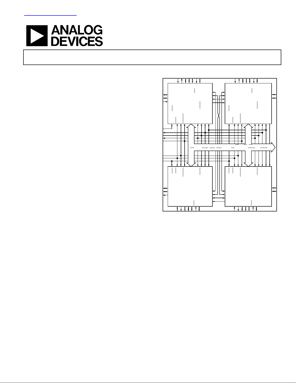
Quad-SHARC
®
DSP Multiprocessor Family
AD14060/AD14060L
FUNCTIONAL BLOCK DIAGRAM
2–0
2, 0
IRQ
LINK 3
LINK 4
LINK 0
FLAG
LINK 2
LINK 5
2–0
LINK 4
IRQ
SPORT 0
SPORT 0
2, 0
FLAG
TDO
3
TCK, TMS, TRST
FLAG1FLAG
ADDR
1
3
TRSTTMS,TCK,
FLAG
FLAG
LINK 0
LINK 2
LINK 5
TDI
= 1)
SHARC BUS (
SW, ACK, SBTS, HBR, HBG, REDY, BR
= 4)
LINK 3
31–0
,
DATA
LINK 0
LINK 2
LINK 5
TDI
LINK 0
LINK 2
LINK 5
TDO
EBOOT,
LBOOT, BMS
,
47–0
,
6–1
EBOOT,
LBOOT, BMS
CS
TIMEXP
SHARC_B
(ID
EMU
CLKIN
MS
3-0
, RPBA, DMAR
EMU
CLKIN
SHARC_C
(ID
CS
TIMEXP
CPA
SPORT 1
TDI
EBOOT,
LBOOT, BMS
EBOOT,
LBOOT, BMS
CPA
SPORT 1
TDO
CS
LINK 1
TIMEXP
SHARC_A
(ID
2–0
EMU
CLKIN
RESET
EMU
CLKIN
RESET
SHARC_D
(ID
2–0
CS
TIMEXP
LINK 1
AD14060/AD14060L
Figure 1.
32 address) is also brought off-module for interfacing with
expansion memory or other peripherals.
The ADSP-21060 link ports are interconnected to provide direct
communication among the four SHARCs, as well as high speed
off-module access. Internally, each SHARC has a direct link port
connection. Externally, each SHARC has a total of 120 Mbytes/s
link port bandwidth.
Multiprocessor performance is enhanced with embedded power
and ground planes, matched impedance interconnect, and
optimized signal routing lengths and separation. The fully
tested and ready-to-insert multiprocessor also significantly
reduces board space.
2–0
2, 0
LINK 1
LINK 3
LINK 4
IRQ
CPA
FLAG
SPORT 1
= 2)
2–0
RESET
SPORT 0
TCK, TMS, TRST
FLAG1FLAG3TDO
,
RD, WR, PAGE, ADRCLK,
RESET
2–0
LINK 1
= 3)
LINK 3
LINK 4
2–0
IRQ
1.2
SPORT 0
FLAG
, DMAG
1
TRSTTMS,TCK,
FLAG
CPA
SPORT 1
2, 0
FLAG
00667-001
)
1.2
3
TDI
Rev. B
Information furnished by Analog Devices is believed to be accurate and reliable.
However, no responsibility is assumed by Analog Devices for its use, nor for any
infringements of patents or other rights of third parties that may result from its use.
Specifications subject to change without notice. No license is granted by implication
or otherwise under any patent or patent rights of Analog Devices. Trademarks and
registered trademarks are the property of their respective owners.
One Technology Way, P.O. Box 9106, Norwood, MA 02062-9106, U.S.A.
Tel: 781.329.4700
Fax: 781.326.8703 © 2004 Analog Devices, Inc. All rights reserved.
www.analog.com

AD14060/AD14060L
TABLE OF CONTENTS
Specifications..................................................................................... 3
Link Port I/O............................................................................... 38
Electrical Characteristics (3.3 V, 5 V Supply)............................ 3
Explanation of Test Levels........................................................... 4
Timing Specifications....................................................................... 5
Memory Read—Bus Master ........................................................ 8
Memory Write—Bus Master ....................................................... 9
Synchronous Read/Write—Bus Master................................... 10
Synchronous Read/Write—Bus Slave ...................................... 12
Multiprocessor Bus Request and Host Bus Request .............. 13
Asynchronous Read/Write—Host to AD14060/AD14060L.15
Three-State Timing—Bus Master, Bus Slave,
DMA Handshake ........................................................................ 18
Absolute Maximum Ratings.......................................................... 27
ESD Caution................................................................................ 27
Pin Configuration and Function Descriptions........................... 28
Pin Function Descriptions ........................................................ 30
HBR, SBTS
..... 17
Serial Ports .................................................................................. 38
Program Booting........................................................................ 38
Host Processor Interface ........................................................... 39
Direct Memory Access (DMA) Controller............................. 39
Applications..................................................................................... 40
Development Tools .................................................................... 40
Quad-SHARC Development Board......................................... 40
Other Package Details................................................................ 40
Target Board Connector for Emulator Probe......................... 40
Output Drive Currents .............................................................. 42
Power Dissipation ...................................................................... 42
Test Conditions........................................................................... 43
Assembly Recommendations.................................................... 45
PCB Layout Guidelines.............................................................. 46
Mechanical Characteristics ....................................................... 47
Detailed Description ...................................................................... 34
Architectural Features................................................................ 34
Shared Memory Multiprocessing ............................................. 34
Off-Module Memor y and Peripherals Interface .................... 36
REVISION HISTORY
12/04—Rev. A to Rev. B
Format Updated..................................................................Universal
Changes to Specifications Section.................................................. 3
Changes to Development Tools Section ......................................40
Changes to Target Board for Emulator Probe Section .............. 40
Changes to Figure 27...................................................................... 42
Updated Outline Dimensions....................................................... 48
Changes to Ordering Guide.......................................................... 48
10/97—Rev. 0 to Rev. A
4/97—Revision 0: Initial Version
Additional Information ............................................................. 47
Outline Dimensions....................................................................... 48
Ordering Guide .......................................................................... 48
Rev. B | Page 2 of 48
AD14060/AD14060L
SPECIFICATIONS
Table 1. Recommended Operating Conditions
B Grade K Grade
Parameter
V
Supply Voltage (5 V) 4.75 5.25 4.75 5.25 V
DD
Min Max Min Max
Supply Voltage (3.3 V) 3.15 3.6 3.15 3.6 V
T
Case Operating Temperature −40 +100 0 +85 °C
CASE
ELECTRICAL CHARACTERISTICS (3.3 V, 5 V SUPPLY)
Table 2.
Test
Level
Test Condition
= max, VIN = 0 V 10 10 µA
DD
= max, VIN = 0 V 150 150 µA
DD
= max, VIN = 0 V 600 600 µA
DD
= max, VIN = VDD max 350 350 µA
DD
Min Typ Max Min Typ Max
350 350 µA
V
= 1.5 V (5 V), 2 V (3.3 V)
IN
= max, VIN = 0 V 4.2 4.2 mA
DD
= max, VIN = 0 V 150 150 µA
DD
= max, VIN = 0 V 600 600 µA
DD
Parameter
V
V
V
V
V
I
I
I
I
I
I
I
I
I
I
I
I
I
I
C
High Level Input Voltage
IH1
High Level Input Voltage
IH2
IL
Low Level Input Voltage
High Level Output Voltage
OH
OL
Low Level Output Voltage
High Level Input Current
IH
IL
Low Level Input Current5
ILP
Low Level Input Current6
ILPX4
Low Level Input Current7
Three-State Leakage Current
OZH
OZL
Three-State Leakage Current
OZHP
Three-State Leakage Current12
Three-State Leakage Current
OZLC
Three-State Leakage Current
OZLA
OZLAR
Three-State Leakage Current10
OZLS
Three-State Leakage Current9
OZLSX4
Three-State Leakage Current11
Supply Current (Internal)
DDIN
Supply Current (Idle)
DDIDLE
Input Capacitance
IN
17, 18
Case
Temp
1
2
1, 2
3, 4
3, 4
5, , 6 7
Full I @ VDD = max 2.0 VDD + 0.5 2.0 VDD + 0.5 V
Full I @ VDD = max 2.2 VDD + 0.5 2.2 VDD + 0.5 V
Full I @ VDD = min 0.8 0.8 V
Full I @ VDD = min, IOH = −2.0 mA4 4.1 2.4 V
Full I @ VDD = min, IOL = 4.0 mA4 0.4 0.4 V
Full I @ VDD = max, VIN = VDD max 10 10 µA
Full I @ V
Full I @ V
Full I @ V
8, , , 9 10 11
8, 12
Full I @ VDD = max, VIN = VDD max 10 10 µA
Full I @ VDD = max, VIN = 0 V 10 10 µA
Full I @ V
13
14
Full I @ VDD = max, VIN = 0 V 1.5 1.5 mA
Full I @ VDD = max,
Full I @ V
Full I @ V
Full I @ V
15
16
Full IV tCK = 25 ns, VDD = max 1.4 2.92 1.0 2.2 A
Full I VDD = max 800 760 mA
25°C V 15 15 pF
1
Applies to input and bidirectional pins: DATA
TFSy1, RFS0, RFSy1, LyxDAT
RCLKy1.
2
Applies to input pins: CLKIN,
3
Applies to output and bidirectional pins: DATA
,
y, DTO, DTy1, TCLK0, TCLKy1, RCLK0, RCLKy1, TFS0, TFSy1, RFS0, RFSy1, LyxDAT
CPA
BR
6-1
4
See the section for typical drive current capabilities. Output Drive Currents
5
Applies to input pins:
6
Applies to input pins with internal pull-ups: DR0, DRy1, TDI.
7
Applies to bused input pins with internal pull-ups:
8
Applies to three-statable pins: DATA
. (Note that ACK is pulled up internally with 2 kΩ during reset in a multiprocessor system, when ID
EMU
mastership.
9
Applies to three-statable pins with internal pull-ups: DTy1, TCLKy1, RCLKy1.
10
Applies to ACK pin when pulled up. (Note that ACK is pulled up internally with 2 kΩ during reset in a multiprocessor system, when ID
ADSP-2106x is not requesting bus mastership.)
11
Applies to bused three-statable pins with internal pull-ups: DT0, TCLK0, RCLK0.
12
Applies to three-statable pins with internal pull-downs: LyxDAT
13
Applies to
14
Applies to ACK pin, when the keeper latch is enabled.
15
Applies to VDD pins. Conditions of operation: each processor is executing radix-2 FFT butterfly with instruction in cache, one data operand is fetched from each
internal memory block, and one DMA transfer is occurring from/to internal memory at t
16
Applies to VDD pins. Idle denotes AD14060/AD14060L state during execution of IDLE instruction.
17
Applies to all signal pins.
18
Guaranteed, but not tested.
HBG
CPA
and
y pin.
, LyxCLK, LyxACK, EBOOTA, LBOOTA, EBOOTBCD, LBOOTBCD,
3-0
RESET, TRST
y
STBS, IRQ
EMU
,
HBR, CS
2-0
47-0
are not tested for leakage current.)
47-0
.
47-0
y,
DMAR1, DMAR2
, ADDR
31-0
, ADDR
, RD, WR, SW, ACK,
31-0
STBS, IRQ
y
, FLAGy0, FLAG1, FLAGy2,
2-0
BMSA, BMSBCD
, ADDR
,
, RD, WR, PAGE, ADRCLK, SW, ACK, FLAGy0, FLAG1, FLAGy2, TIMEXPy,
MS
31-0
3-0
, LyxCLK, LyxACK,
3-0
, RPBA, EBOOTA, LBOOTA, EBOOTBCD, LBOOTBCD, CLKIN,
, TMS.
TRST
,
, RD, WR, PAGE, ADRCLK, SW, ACK, FLAGy0, FLAG1, FLAGy2, REDY,
MS
3-0
2-0
, LyxCLK, LyxACK.
3-0
= 25 ns.
CK
5 V 3.3 V
, CSy,
HBG
, TMS, TDI, TCK,
BMSA, BMSBCD
RESET
DMAR1, DMAR2, BR
, DR0, DRy1, TCLK0, TCLKy1, RCLK0,
HBR
HBG
, TDO,
EMU
.
, TCK.
6-1
, REDY,
, RPBA,
DMAG1, DMAG2
HBG, DMAG1, DMAG2, BMSA, BMSBCD
= 001 and another ADSP-2106x is not requesting bus
= 001 and another
2-0
CPA
Unit
Unit
y, TFS0,
,
, TDO,
Rev. B | Page 3 of 48

AD14060/AD14060L
EXPLANATION OF TEST LEVELS
Test Level
I 100% production tested.
II
100% production tested at 25°C, and sample tested at
specified temperatures.
III Sample tested only.
IV
Parameter is guaranteed by design and analysis, and
characterization testing on discrete SHARCs.
V Parameter is typical value only.
VI
All devices are 100% production tested at 25°C, and
sample tested at temperature extremes.
1
Link and serial ports: All are 100% tested at die level prior to assembly. All are
100% ac tested at module level; Link 4 and Serial 0 are also dc tested at the
module level. See the section.
Timing Specifications
1
Rev. B | Page 4 of 48
AD14060/AD14060L
TIMING SPECIFICATIONS
This data sheet represents production-released specifications
for the AD14060 (5 V), and for the AD14060L (3.3 V). The
ADSP-21060 die components are 100% tested, and the
assembled AD14060/AD14060L units are again extensively
tested at speed and across temperature. Parametric limits were
established from the ADSP-21060 characterization followed by
further design and analysis of the AD14060/AD14060L package
characteristics.
The specifications are based on a CLKIN frequency of 40 MHz
= 25 ns). The DT derating allows specifications at other
(t
CK
CLKIN frequencies (within the minimum to maximum range
of the t
specification; see Table 3). DT is the difference
CK
between the actual CLKIN period and a CLKIN period of 25 ns:
DT = t
− 25 ns
CK
Use the exact timing information given. Do not attempt to
derive parameters from the addition or subtraction of others.
While addition or subtraction would yield meaningful results
for an individual device, the values given in this data sheet
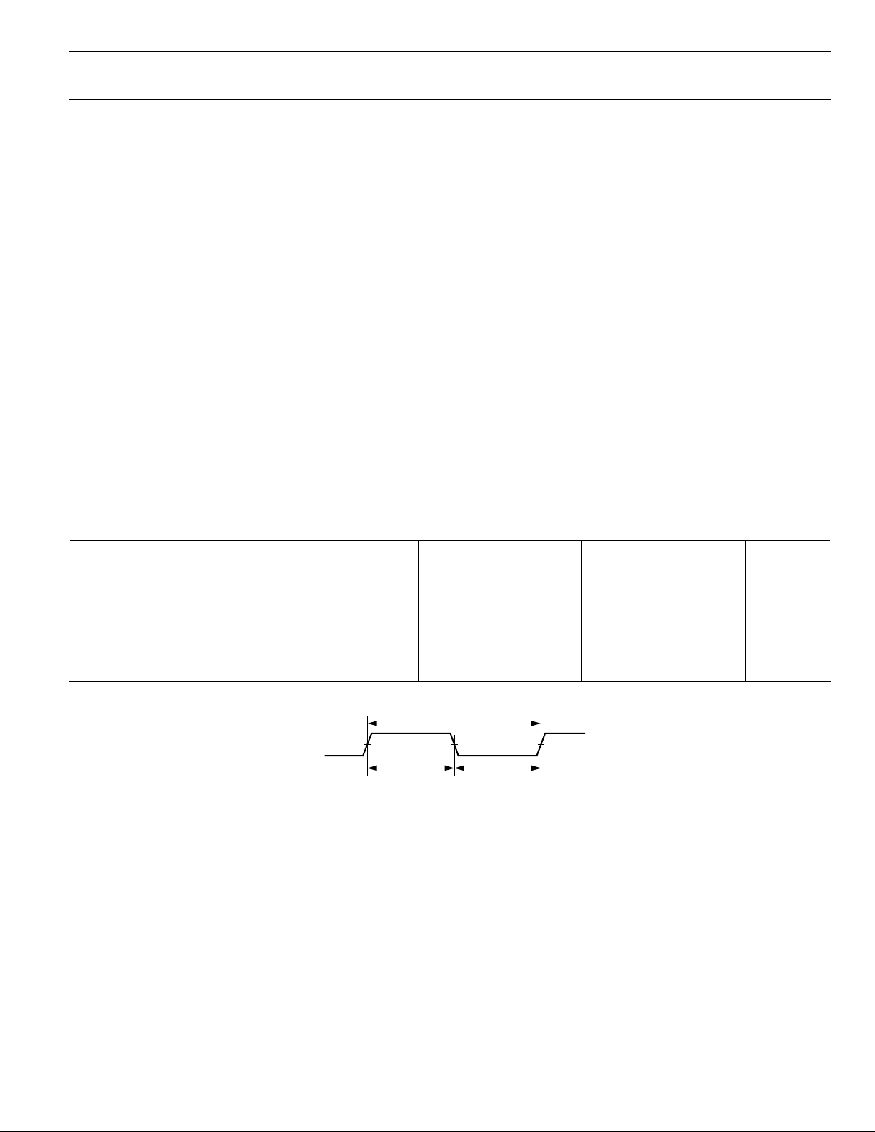
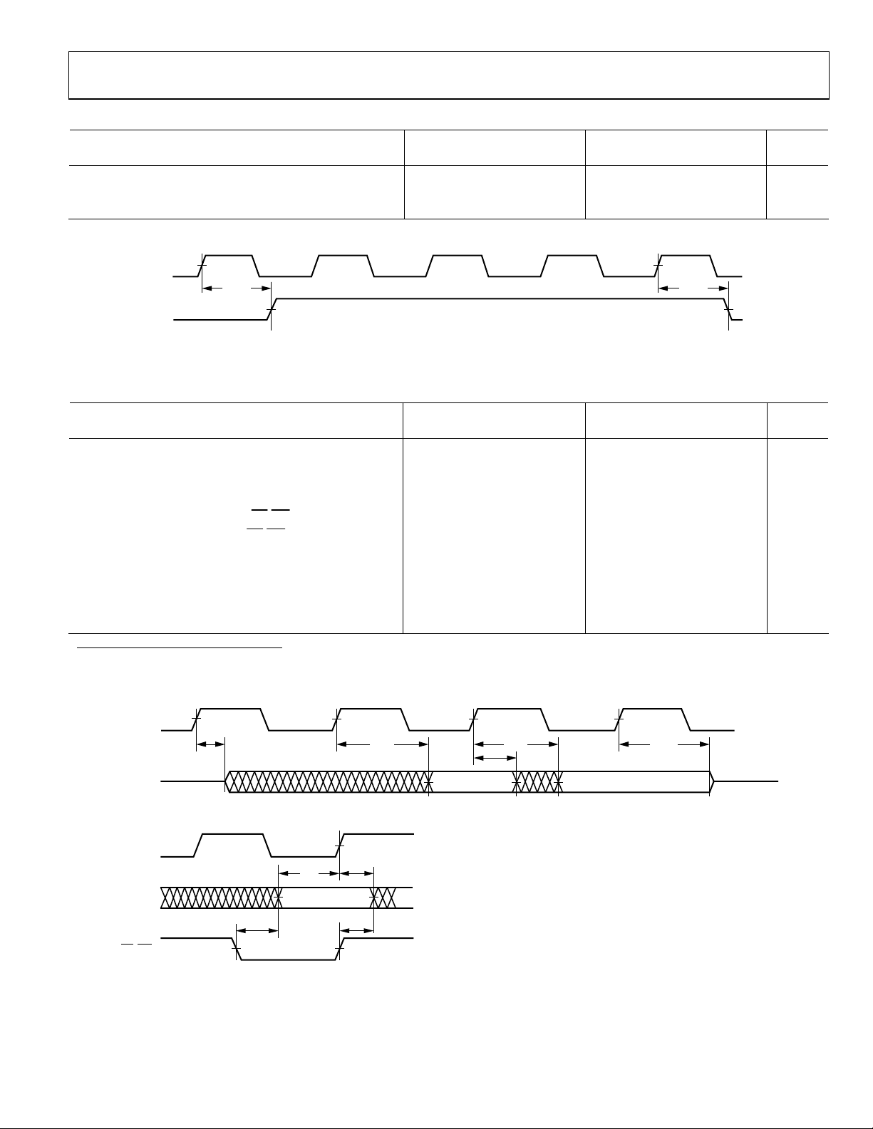
Table 3. Clock Input
Parameter
Clock Input
Timing Requirements:
t
t
t
t
CK
CKL
CKH
CKRF
CLKIN Period 25 100 25 100 ns
CLKIN Width Low 7 9.5 ns
CLKIN Width High 5 5 ns
CLKIN Rise/Fall (0.4 V to 2.0 V) 3 3 ns
Min Max Min Max
reflect statistical variations and worst cases. Consequently, one
cannot meaningfully add parameters to derive longer times.
Switching Characteristics specify how the processor changes its
signals. The user has no control over this timing—circuitry
external to the processor must be designed for compatibility
with these signal characteristics. Switching characteristics
specify what the processor does in a given circumstance. The
user can also use switching characteristics to ensure that any
timing requirement of a device connected to the processor
(such as memory) is satisfied.
Timing Requirement s apply to signals that are controlled by
circuitry external to the processor, such as the data input for a
read operation. Timing requirements guarantee that the
processor operates correctly with other devices.
(O/D) = Open Drain
(A/D) = Active Drive
40 MHz (5 V) 40 MHz (3.3 V)
Unit
CLKIN
t
CK
t
CKH
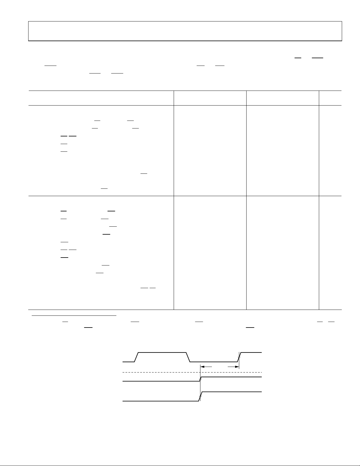
Figure 2. Clock Input
Rev. B | Page 5 of 48
t
CKL
00667-011
AD14060/AD14060L
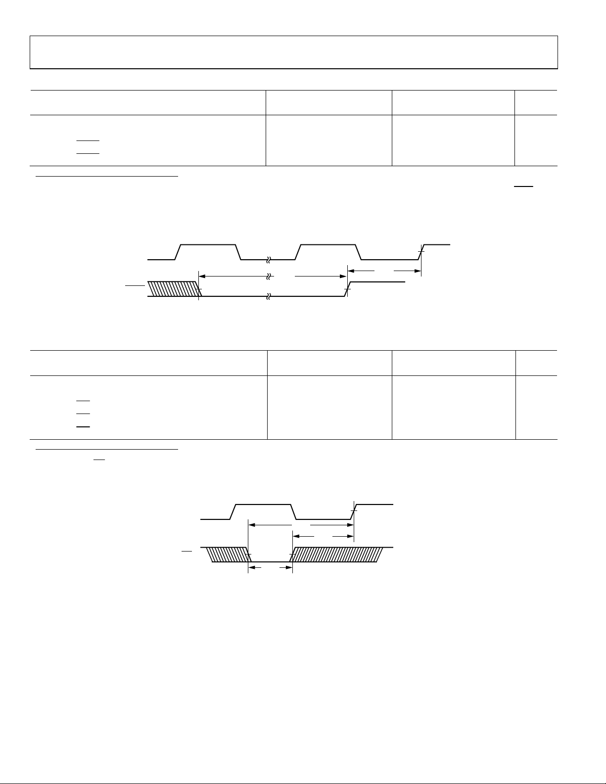
Table 4. Reset
5 V 3.3 V
Parameter
Reset
Timing Requirements:
t
t
WRST
SRST
RESET Pulse Width Low
RESET Setup before CLKIN High
1
2
Min Max Min Max
4 t
CK
14 + DT/2 t
4 t
CK
14 + DT/2 t
CK
ns
CK
1
Applies after the power-up sequence is complete. At power-up, the processor’s internal phase-locked loop requires no more than 2000 CLKIN cycles while
low, assuming stable V
2
Only required if multiple ADSP-2106xs must come out of reset synchronous to CLKIN with program counters (PC) equal (that is, for a SIMD system). Not required for
and CLKIN (not including start-up time of the external clock oscillator).
DD
multiple ADSP-2106xs communicating over the shared bus (through the external port), because the bus arbitration logic automatically synchronizes itself after reset.
CLKIN
t
SRST
00667-012
RESET
t
WRST
Figure 3. Reset
Table 5. Interrupts
5 V 3.3 V
Parameter Min Max Min Max Unit
Interrupts
Timing Requirements:
t
SIR
t
HIR
t
IPW
IRQ2-0 Setup before CLKIN High
IRQ2-0 Hold before CLKIN High1
IRQ2-0 Pulse Width
1
2
18 + 3 DT/4 18 + 3 DT/4 ns
11.5 + 3 DT/4 11.5 + 3 DT/4 ns
2 + t
CK
2 + t
CK
ns
Unit
ns
RESET
is
1
Only required for
2
Applies only if t
x recognition in the following cycle.
IRQ
and t
requirements are not met.
SIR
HIR
CLKIN
IRQ
2–0
t
SIR
t
IPW
Figure 4. Interrupts
t
HIR
00667-013
Rev. B | Page 6 of 48
AD14060/AD14060L
Table 6. Timer
5 V 3.3 V
Parameter
Timer
Switching Characteristic:
t
DTEX
CLKIN High to TIMEXP 16 16 ns
Min Max Min Max
CLKIN
t
DTEX
TIMEXP
Figure 5. Timer
Table 7. Flags
5 V 3.3 V
Parameter
Flags
Timing Requirements:
t
SFI
t
HFI
t
DWRFI
t
HFIWR
FLAG2-0IN Setup before CLKIN High
FLAG2-0IN Hold after CLKIN High1 0.5 − 5 DT/16 0.5 − 5 DT/16 ns
FLAG2-0IN Delay after RD/WR Low1
FLAG2-0IN Hold after RD/WR De-asserted1
Switching Characteristics:
t
t
t
t
DFO
HFO
DFOE
DFOD
FLAG2-0
FLAG2-0
Delay after CLKIN High 17 17 ns
OUT
Hold after CLKIN High 4 4 ns
OUT
CLKIN High to FLAG2-0
CLKIN High to FLAG2-0
1
Enable 3 3 ns
OUT
Disable 15 15 ns
OUT
Min Max Min Max
8 + 5 DT/16 8 + 5 DT/16 ns
4.5 + 7 DT/16 4.5 + 7 DT/16 ns
0.5 0.5 ns
1
Flag inputs that meet these setup and hold times affect conditional instructions in the following instruction cycle.
t
DTEX
00667-014
Unit
Unit
FLAG2–0
FLAG2–0
RD, WR
CLKIN
OUT
CLKIN
t
DFOE
t
SFI
IN
t
DWRFI
FLAG INPUT
t
HFI
t
HFIWR
t
DFO
t
HFO
FLAG OUTPUT
t
DFO
t
DFOD
00667-015
Figure 6. Flags
Rev. B | Page 7 of 48
AD14060/AD14060L
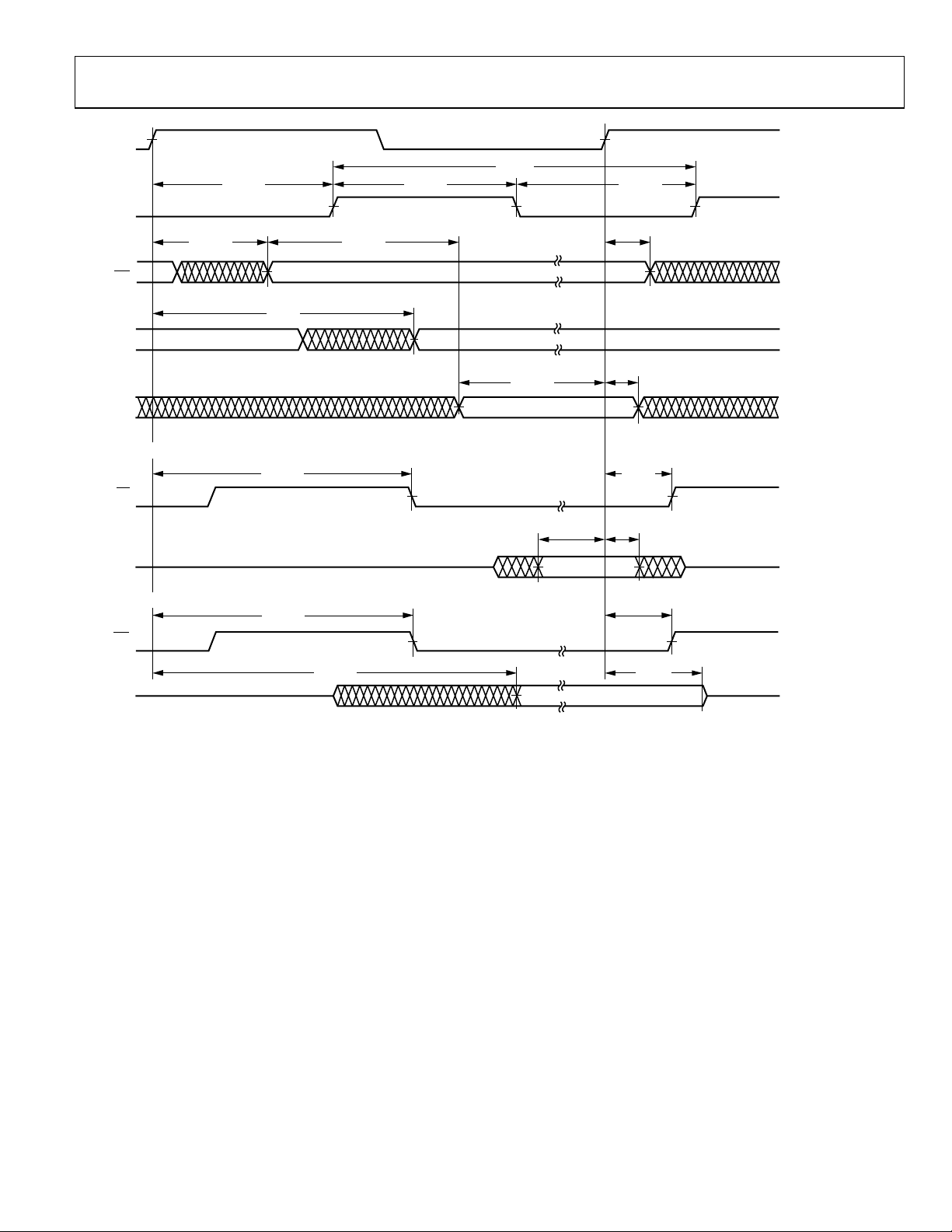
MEMORY READ—BUS MASTER
Use these specifications for asynchronous interfacing to memories (and memory-mapped peripherals) without reference to CLKIN.
These specifications apply when the AD14060/AD14060L is the bus master accessing external memory space.
These switching characteristics also apply for bus master synchronous read/write timing (see the Synchronous Read/Write—Bus Master
section). If these timing requirements are met, the synchronous read/write timing can be ignored (and vice versa).
Table 8. Specifications
5 V 3.3 V
Parameter
Timing Requirements:
t
t
t
t
t
t
DAD
DRLD
HDA
HDRH
DAAK
DSAK
Address, Delay to Data Valid
RD Low to Data Valid1
Data Hold from Address
Data Hold from RD High3
ACK Delay from Address
ACK Delay from RD Low4
Switching Characteristics:
t
DRHA
t
DARL
t
RW
t
RWR
t
SADADC
Address Hold after RD High
Address to RD Low2
RD Pulse Width
RD High to WR, RD, DMAGx Low
Address Setup before ADRCLK High2 −0.5 + DT/4 −0.5 + DT/4 ns
1, 2
3
2, 4
Min Max Min Max
17.5 + DT + W 17.5 + DT + W ns
11.5 + 5 DT/8 + W 11.5 + 5 DT/8 + W ns
1 1 ns
2.5 2.5 ns
13.5 + 7 DT/8 + W 13.5 + 7 DT/8 + W ns
7.5 + DT/2 + W 7.5 + DT/2 + W ns
−0.5 + H −0.5 + H ns
1.5 + 3 DT/8 1.5 + 3 DT/8 ns
12.5 + 5 DT/8 + W 12.5 + 5 DT/8 + W ns
8 + 3 DT/8 + HI 8 + 3 DT/8 + HI ns
W = number of wait states specified in WAIT register × t
, if an address hold cycle or bus idle cycle occurs, as specified in WAIT register; otherwise, HI = 0.
HI = t
CK
, if an address hold cycle occurs as specified in WAIT register; otherwise, H = 0.
H = t
CK
.
CK
1
Data delay/setup: User must meet t
2
For MSx, SW,
3
Data hold: User must meet t
capacitive and dc loads.
4
ACK delay/setup: User must meet t
, the falling edge is referenced.
BMS
HDA
, t
, or synchronous specification, t
DAD
DRLD
, t
, or synchronous specification, t
HDRH
, t
, or synchronous specification, t
DSAK
DAAK
.
SSDATI
. See the section for the calculation of hold times given
HDATI
System Hold Time Calculation Example
.
SACKC
ADDRESS
MSx, SW
BMS
RD
DATA
ACK
t
DARL
t
DAAK
t
t
DAD
DSAK
t
DRLD
t
t
HDRH
DRHA
t
HDA
t
RWR
t
RW
Unit
WR, DMAG
ADRCLK
(OUT)
t
SADADC
00667-016
Figure 7. Memory Read—Bus Master
Rev. B | Page 8 of 48
AD14060/AD14060L
MEMORY WRITE—BUS MASTER
Use these specifications for asynchronous interfacing to memories (and memory-mapped peripherals) without reference to CLKIN.
These specifications apply when the AD14060/AD14060L is the bus master accessing external memory space.
These switching characteristics also apply for bus master synchronous read/write timing (see the Synchronous Read/Write—Bus Master
section). If these timing requirements are met, the synchronous read/write timing can be ignored (and vice versa).
Table 9. Specifications
5 V 3.3 V
Parameter
Timing Requirements:
t
t
DAAK
DSAK
ACK Delay from Address, Selects
ACK Delay from WR Low1
Switching Characteristics:
t
DAWH
t
DAWL
t
WW
t
DDWH
t
DWHA
t
DATRWH
t
WWR
t
DDWR
t
WDE
t
SADADC
Address, Selects to WR
2
De-asserted
Address, Selects to WR Low2
WR Pulse Width
Data Setup before WR High
Address Hold after WR De-asserted
Data Disable after WR De-asserted
WR High to WR, RD, DMAGx Low
Data Disable before WR or RD Low
WR Low to Data Enabled
Address, Selects to ADRCLK High2 −0.5 + DT/4 −0.5 + DT/4 ns
Min Max Min Max
1, 2
13.5 + 7 DT/8 + W 13.5 + 7 DT/8 + W ns
8 + DT/2 + W 8 + DT/2 + W ns
16.5 + 15 DT/16 + W 16.5 + 15 DT/16 + W ns
2.5 + 3 DT/8 2.5 + 3 DT/8 ns
12 + 9 DT/16 + W 12 + 9 DT/16 + W ns
6.5 + DT/2 + W 6.5 + DT/2 + W ns
0 + DT/16 + H 0 + DT/16 + H ns
3
0.5 + DT/16 + H 6.5 + DT/16 + H 0.5 + DT/16 + H 6.5 + DT/16 + H ns
8 + 7 DT/16 + H 8 + 7 DT/16 + H ns
4.5 + 3 DT/8 + 1 4.5 + 3 DT/8 + 1 ns
−1.5 + DT/16 −1.5 + DT/16 ns
W = number of wait states specified in WAIT register × t
, if an address hold cycle occurs, as specified in WAIT register; otherwise, H = 0.
H = t
CK
, if a bus idle cycle occurs, as specified in WAIT register; otherwise, I = 0.
I = t
CK
.
CK
1
ACK delay/setup: User must meet t
2
For MSx, SW,
3
See the section for the calculation of hold times given capacitive and dc loads. System Hold Time Calculation Example
, the falling edge is referenced.
BMS
, t
, or synchronous specification, t
DAAK
DSAK
ADDRESS
MSx, SW
BMS
t
DAWL
WR
t
WDE
DATA
ACK
t
DAAK
t
DSAK
SACKC
t
DAWH
.
t
t
DATRWH
DWHA
t
WWR
t
DDWR
t
WW
t
DDWH
Unit
RD, DMAG
ADRCLK
(OUT)
t
SADADC
00667-017
Figure 8. Memory Write—Bus Master
Rev. B | Page 9 of 48
AD14060/AD14060L
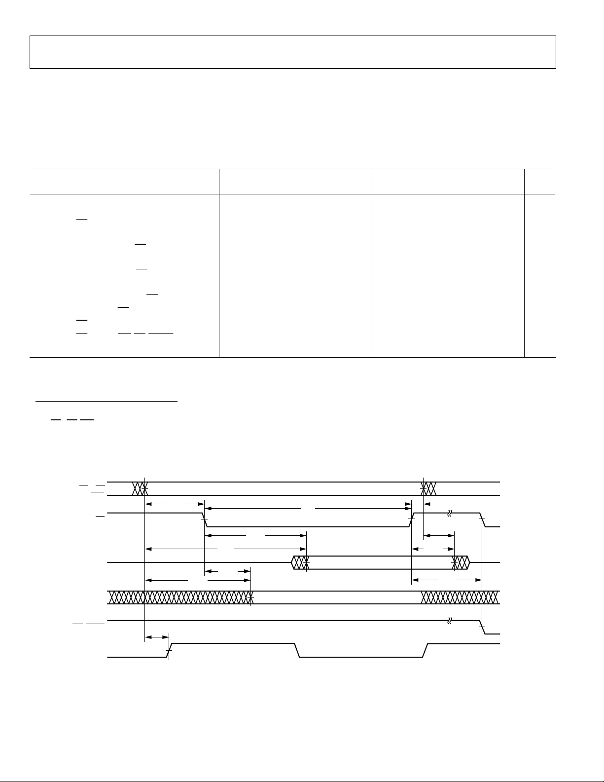
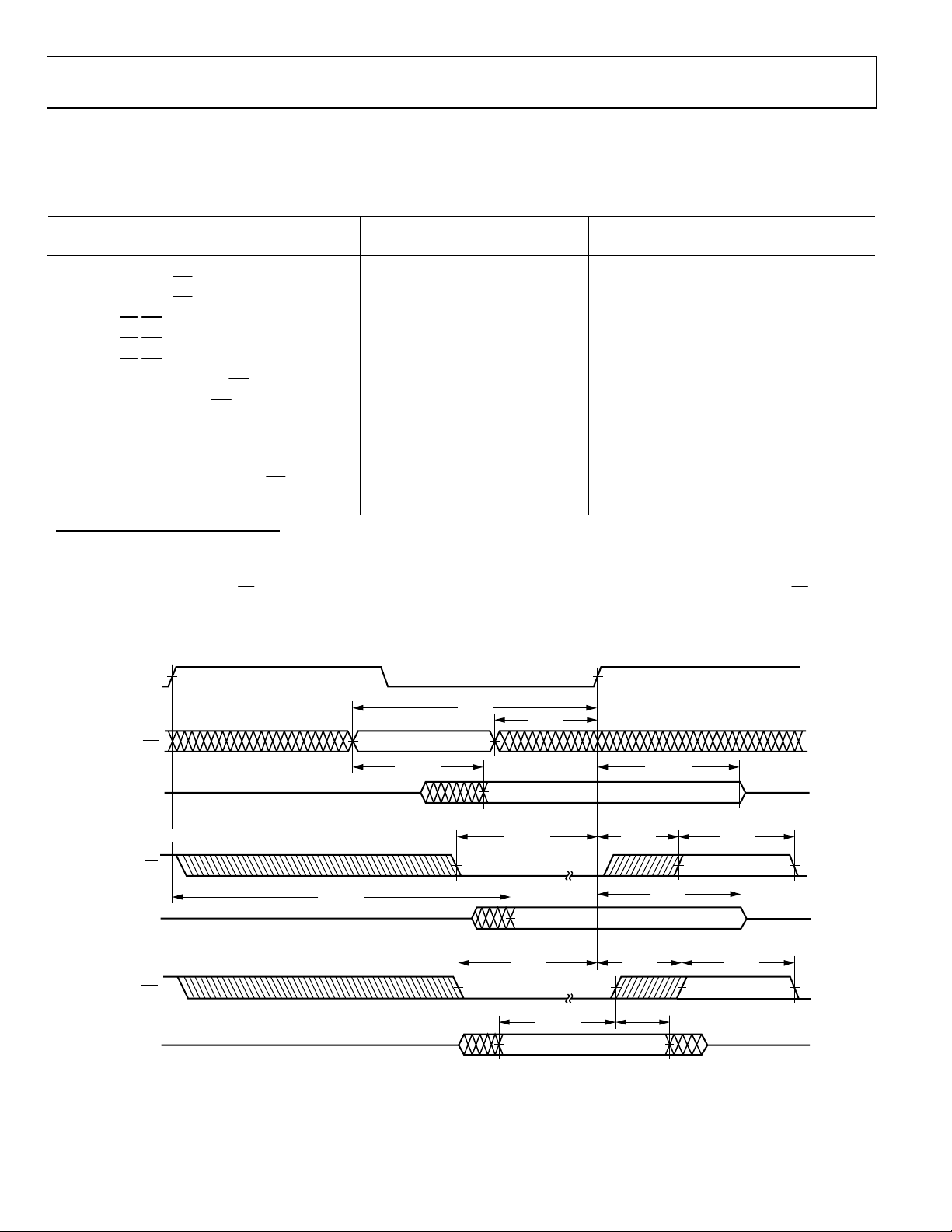
SYNCHRONOUS READ/WRITE—BUS MASTER
Use these specifications for interfacing to external memory systems that require CLKIN—relative timing or for accessing a slave
ADSP 2106x in multiprocessor memory space. These synchronous switching characteristics are also valid during asynchronous memory
reads and writes (see the Memory Read—Bus Master and Memory Write—Bus Master sections).
When accessing a slave ADSP-2106x, these switching characteristics must meet the slave’s timing requirements for synchronous
read/writes (see the Synchronous Read/Write—Bus Slave section). The slave ADSP-2106x must also meet these bus master timing
requirements for data and acknowledge setup and hold times.
Table 10. Specifications
5 V 3.3 V
Parameter
Timing Requirements:
t
SSDATI
t
HSDATI
t
DAAK
t
SACKC
t
HACKC
Data Setup before CLKIN 3 + DT/8 3 + DT/8 ns
Data Hold after CLKIN 4 − DT/8 4 − DT/8 ns
ACK Delay after Address, MSx, SW, BMS
ACK Setup before CLKIN2 6.5 + DT/4 6.5 + DT/4 ns
ACK Hold after CLKIN −0.5 − DT/4 −0.5 − DT/4 ns
Switching Characteristics:
t
DADRO
t
HADRO
t
DPGC
t
DRDO
t
DWRO
t
DRWL
t
SDDATO
t
DATTR
t
DADCCK
t
ADRCK
t
ADRCKH
t
ADRCKL
W = number of wait states specified in WAIT register × t
Address, MSx, BMS, SW, Delay after CLKIN1
Address, MSx, BMS, SW, Hold after CLKIN
PAGE Delay after CLKIN 9 + DT/8 17 + DT/8 9 + DT/8 17 + DT/8 ns
RD High Delay after CLKIN
WR High Delay after CLKIN
RD/WR Low Delay after CLKIN
Data Delay after CLKIN 20 + 5 DT/16 20.25 + 5 DT/16 ns
Data Disable after CLKIN
3
ADRCLK Delay after CLKIN 4 + DT/8 11 + DT/8 4 + DT/8 11 + DT/8 ns
ADRCLK Period t
ADRCLK Width High (tCK/2 − 2) (tCK/2 − 2) ns
ADRCLK Width Low (tCK/2 − 2) (tCK/2 − 2) ns
1
For MSx, SW,
2
ACK delay/setup: User must meet t
3
See the section for the calculation of hold times given capacitive and dc loads. System Hold Time Calculation Example
, the falling edge is referenced.
BMS
DAAK
, t
, or synchronous specification, t
DSAK
Min Max Min Max
1, 2
13.5 + 7 DT/8 + W 13.5 + 7 DT/8 + W ns
8 − DT/8 8 − DT/8 ns
−1 − DT/8 −1 − DT/8 ns
−2 − DT/8 +5 − DT/8 −2 − DT/8 +5 − DT/8 ns
−3 − 3 DT/16 +5 − 3 DT/16 −3 − 3 DT/16 +5 − 3 DT/16 ns
8 + DT/4 13.5 + DT/4 8 + DT/4 13.5 + DT/4 ns
0 − DT/8 8 − DT/8 0 − DT/8 8 – DT/8 ns
CK
.
CK
SACKC
t
.
CK
ns
Unit
Rev. B | Page 10 of 48
AD14060/AD14060L
CLKIN
t
ADRCK
t
SACKC
t
HADRO
t
HACKC
t
SSDATItHSDATI
t
ADRCKL
t
DRDO
ADRCLK
ADDRESS
SW
PAGE
ACK
(IN)
READ CYCLE
RD
t
DADRO
t
DADCCK
t
DPGC
t
DRWL
t
DAAK
t
ADRCKH
DATA
(IN)
WRITE CYCLE
WR
DATA
(OUT)
t
DRWL
t
SDDATO
Figure 9. Synchronous Read/Write—Bus Master
t
DWRO
t
DATTR
00667-018
Rev. B | Page 11 of 48
AD14060/AD14060L
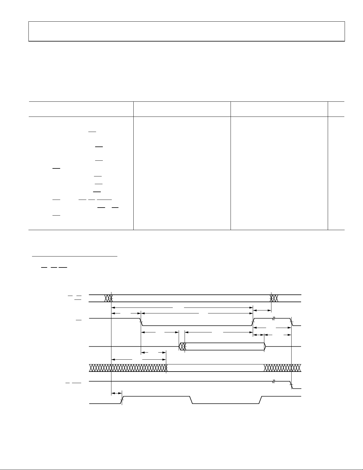
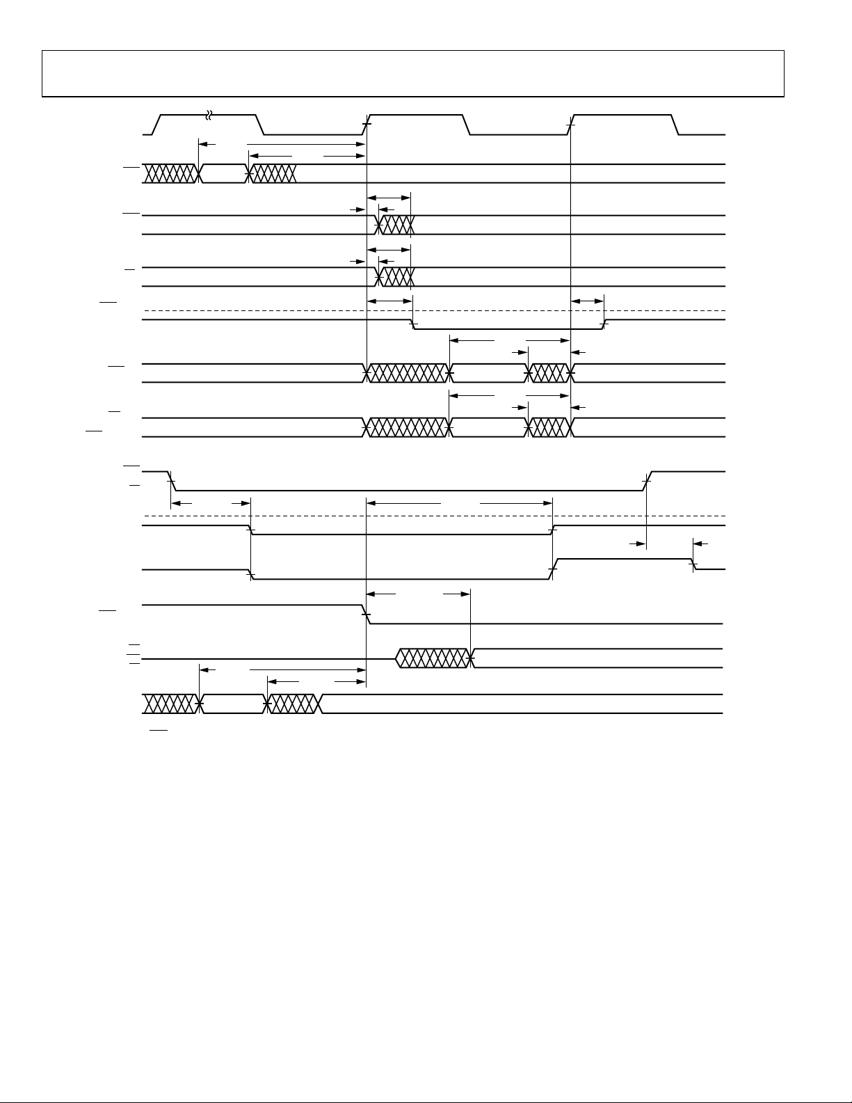
SYNCHRONOUS READ/WRITE—BUS SLAVE
Use these specifications for bus master access to a slave’s IOP registers or internal memory in multiprocessor memory space. The bus
master must meet these bus slave timing requirements.
Table 11. Specifications
5 V 3.3 V
Parameter
Timing Requirements:
t
SADRI
t
HADRI
t
SRWLI
t
HRWLI
t
RWHPI
t
SDATWH
t
HDATWH
Address, SW Setup before CLKIN
Address, SW Hold before CLKIN
RD/WR Low Setup before CLKIN
RD/WR Low Hold after CLKIN
RD/WR Pulse High
Data Setup before WR High
Data Hold after WR High
Switching Characteristics:
t
SDDATO
t
DATTR
t
DACKAD
t
ACKTR
Data Delay after CLKIN 20 + 5 DT/16 20.25 + 5 DT/16 ns
Data Disable after CLKIN
ACK Delay after Address, SW
ACK Disable after CLKIN3 −1 − DT/8 +7 − DT/8 −1 − DT/8 +7 − DT/8 ns
1
2
3
Min Max Min Max
15.5 + DT/2 15.5 + DT/2 ns
4.5 + DT/2 4.5 + DT/2 ns
9.5 + 5 DT/16 9.5 + 5 DT/16 ns
−3.5 − 5 DT/16 +8 + 7 DT/16 −3.25 − 5 DT/16 +8 + 7 DT/16 ns
3 3 ns
5.5 5.5 ns
1.5 1.5 ns
0 − DT/8 8 − DT/8 0 − DT/8 8 − DT/8 ns
10 10 ns
1
t
(min) = 9.5 + 5 DT/16 when the multiprocessor memory space wait state (MMSWS bit in WAIT register) is disabled; when MMSWS is enabled, t
SRWLI
4 + DT/8.
2
See the section for the calculation of hold times given capacitive and dc loads. System Hold Time Calculation Example
3
t
is true only if the address and SW inputs have setup times (before CLKIN) greater than 10.5 + DT/8 and less than 18.5 + 3 DT/4. If the address and SW inputs have
DACKAD
SRWLI
setup times greater than 19 + 3 DT/4, then ACK is valid 15 + DT/4 (max) after CLKIN. A slave that sees an address with an M field match responds with ACK regardless
of the state of MMSWS or strobes. A slave three-states ACK every cycle with t
ACKTR
.
Unit
(min) =
CLKIN
t
ADDRESS
SW
ACK
READ ACCESS
RD
DATA
(OUT)
WRITE ACCESS
WR
DATA
(IN)
t
SDDATO
t
DACKAD
SADRI
t
SRWLI
t
SRWLI
t
HADRI
t
SDATWH
t
HRWLI
t
HRWLI
t
HDATWH
t
ACKTR
t
DATTR
t
RWHPI
t
RWHPI
00667-019
Figure 10. Synchronous Read/Write—Bus Slave
Rev. B | Page 12 of 48
AD14060/AD14060L
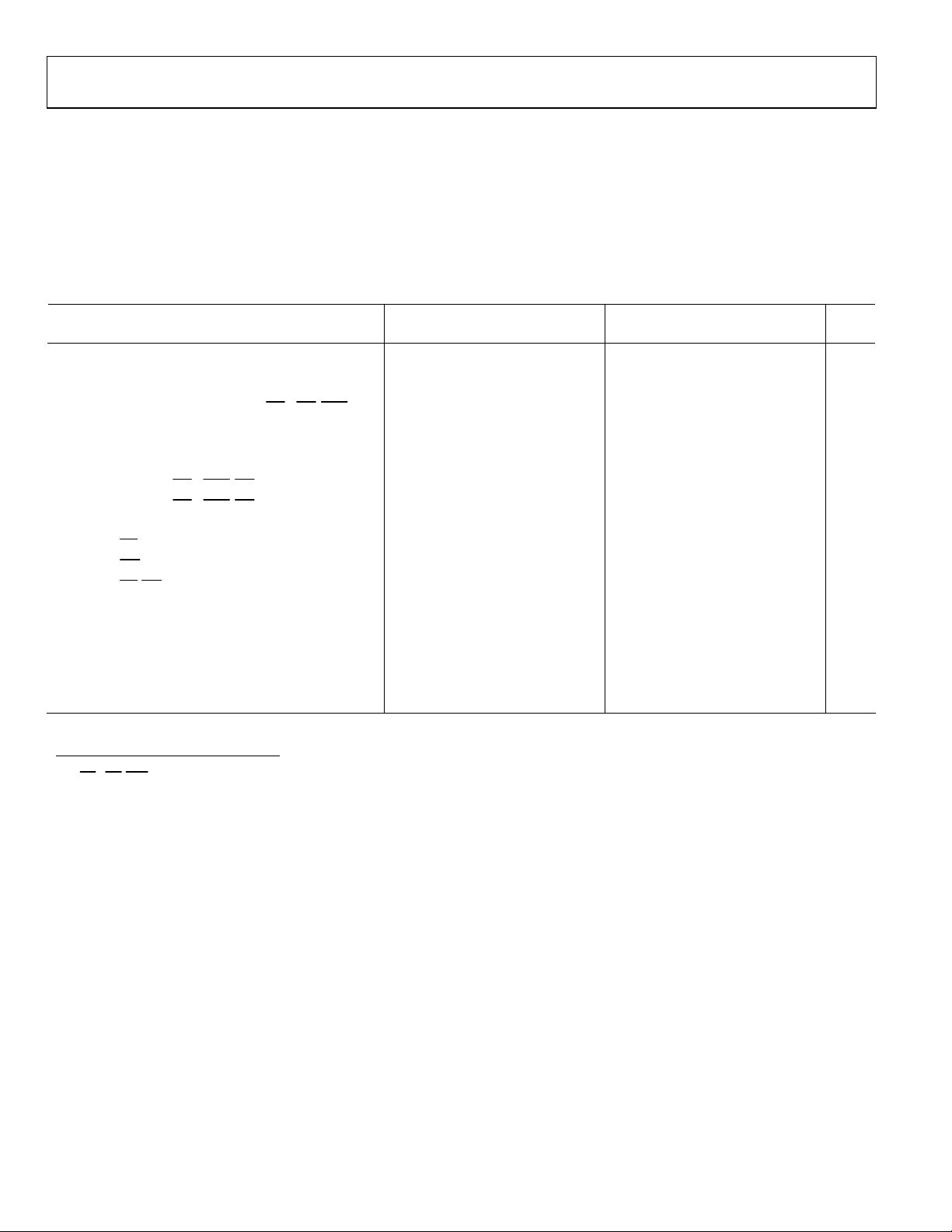
MULTIPROCESSOR BUS REQUEST AND HOST BUS REQUEST
Use these specifications for passing of the bus mastership among multiprocessing ADSP-2106xs (BRx) or a host processor (
Table 12. Specifications
5 V 3.3 V
Parameter
Timing Requirements:
t
HBGRCSV
t
SHBRI
t
HHBRI
t
SHBGI
t
HHBGI
t
SBRI
t
HBRI
t
SRPBAI
t
HRPBAI
HBG Low to RD/WR/CS Valid
HBR Setup before CLKIN
HBR Hold before CLKIN2
HBG Setup before CLKIN
HBG Hold before CLKIN High
BRx, CPA Setup before CLKIN
BRx, CPA Hold before CLKIN High
RPBA Setup before CLKIN 21 + 3 DT/4 21 + 3 DT/4 ns
RPBA Hold before CLKIN 11.5 + 3 DT/4 11.5 + 3 DT/4 ns
Switching Characteristics:
t
DHBGO
t
HHBGO
t
DBRO
t
HBRO
t
DCPAO
t
TRCPA
t
DRDYCS
t
TRDYHG
t
ARDYTR
HBG Delay after CLKIN
HBG Hold after CLKIN
BRx Delay after CLKIN
BRx Hold after CLKIN
CPA Low Delay after CLKIN
CPA Disable after CLKIN
REDY (O/D) or (A/D) Low from CS and HBR Low
REDY (O/D) Disable or REDY (A/D) High from HBG4
REDY (A/D) Disable from CS or HBR High4
1
2
3
4
Min Max Min Max
19.5 + 5 DT/4 19.5 + 5 DT/4 ns
20 + 3 DT/4 20 + 3 DT/4 ns
13.5 + 3 DT/4 13.5 + 3 DT/4 ns
13 + DT/2 13 + DT/2 ns
5.5 + DT/2 5.5 + DT/2 ns
13 + DT/2 13 + DT/2 ns
5.5 + DT/2 5.5 + DT/2 ns
8 − DT/8 8 − DT/8 ns
−2 − DT/8 −2 − DT/8 ns
8 − DT/8 8 − DT/8 ns
−2 − DT/8 −2 − DT/8 ns
9 − DT/8 9.5 − DT/8 ns
–2 − DT/8 +5.5 − DT/8 −2 − DT/8 +5.5 − DT/8 ns
9.5 12 ns
40 + 27 DT/16 40 + 27 DT/16 ns
11 11 ns
HBR, HBG
).
Unit
1
For first asynchronous access after
easily accomplished by driving an upper address signal high when
2
Required only for recognition in the current cycle.
3
assertion must meet the setup to CLKIN; de-assertion does not need to meet the setup to CLKIN.
CPA
4
(O/D) = open drain; (A/D) = active drive.
and CS asserted, ADDR
HBR
must be a non-MMS value 1/2 tCK before RD or WR goes low, or by t
31–0
is asserted.
HBG
after HBG goes low. This is
HBGRCSV
Rev. B | Page 13 of 48
AD14060/AD14060L
CLKIN
HBR
HBG
(OUT)
BRx
(OUT)
CPA (OUT)
(O/D)
HBG (IN)
BRx (IN)
CPA (IN) (O/D)
HBR
CS
REDY (O/D)
REDY (A/D)
t
DRDYCS
t
SHBRI
t
HHBRI
t
HHBGO
t
HBRO
t
DHBGO
t
DBRO
t
DCPAO
t
TRDYHG
t
SHBGI
t
SBRI
t
HHBGI
t
HBRI
t
TRCPA
t
ARDYTR
t
HBGRCSV
HBG (OUT)
RD
WR
CS
RPBA
O/D = OPEN DRAIN, A/D = ACTIVE DRIVE
HBG IS DELAYED BY n CLOCK CYCLES WHEN WAIT STATES OR BUS LOCK ARE IN EFFECT.
t
SRPBAI
t
HRPBAI
00667-020
Figure 11. Multiprocessor Bus Request and Host Bus Request
Rev. B | Page 14 of 48
AD14060/AD14060L
ASYNCHRONOUS READ/WRITE—HOST TO AD14060/AD14060L
Use these specifications for asynchronous host processor access to an AD14060/AD14060L, after the host has asserted CS and
HBG
After
memory or IOP registers.
is returned by the AD14060/AD14060L, the host can drive the RD and WR pins to access the AD14060/AD14060L’s internal
HBR
and
HBG
are assumed low for this timing.
Table 13. Specifications
5 V 3.3 V
Parameter
Read Cycle
Timing Requirements:
t
SADRDL
t
HADRDH
t
WRWH
t
DRDHRDY
t
DRDHRDY
Address Setup/CS Low before RD Low
Address Hold/CS Hold Low after RD
RD/WR High Width
RD High Delay after REDY (O/D) Disable
RD High Delay after REDY (A/D) Disable
Switching Characteristics:
t
SDATRDY
t
DRDYRDL
t
RDYPRD
t
HDARWH
Data Valid before REDY Disable from Low 1.5 1.5 ns
REDY (O/D) or (A/D) Low Delay after RD Low
REDY (O/D) or (A/D) Low Pulse Width for Read 45 + DT 45 + DT ns
Data Disable after RD High
Write Cycle
Timing Requirements:
t
SCSWRL
t
HCSWRH
t
SADWRH
t
HADWRH
t
WWRL
t
WRWH
t
DWRHRDY
t
SDATWH
t
HDATWH
CS Low Setup before WR Low
CS Low Hold after WR High
Address Setup before WR High
Address Hold after WR High
WR Low Width
RD/WR High Width
WR High Delay after REDY (O/D) or (A/D) Disable
Data Setup before WR High
Data Hold After WR High
Switching Characteristics:
t
DRDYWRL
t
RDYPWR
t
SRDYCK
REDY (O/D) or (A/D) Low Delay after WR/CS Low
REDY (O/D) or (A/D) Low Pulse Width for Write 15 15 ns
REDY (O/D) or (A/D) Disable to CLKIN 0 + 7 DT/16 8 + 7 DT/16 0 + 7 DT/16 8 + 7 DT/16 ns
1
Min Max Min Max
0.5 0.5 ns
0.5 0.5 ns
6 6 ns
0 0 ns
0 0 ns
11 13.5 ns
1.5 9 1.5 9.5 ns
0.5 0.5 ns
0.5 0.5 ns
5.5 5.5 ns
2.5 2.5 ns
7 7 ns
6 6 ns
0.5 0.5 ns
5.5 5.5 ns
1.5 1.5 ns
11 13.5 ns
1
Not required, if RD and address are valid t
goes low or by t
during asynchronous host accesses, see the ADSP-2106x SHARC User’s Manual.
HBGRCSV
after
goes low. This is easily accomplished by driving an upper address signal high when
HBG
HBGRCSV
after
goes low. For first access after
HBG
is asserted, ADDR
HBR
must be a non-MMS value 1/2 t
31–0
is asserted. For address bits to be driven
HBG
HBR
before RD or WR
CLK
(low).
Unit
CLKIN
REDY (O/D)
REDY (A/D)
O/D = OPEN DRAIN, A/D = ACTIVE DRIVE
Figure 12. Synchronous REDY Timing
Rev. B | Page 15 of 48
t
SRDYCK
00667-021
AD14060/AD14060L
READ CYCLE
ADDRESS/CS
RD
DATA (OUT)
REDY (O/D)
REDY (A/D)
WRITE CYCLE
ADDRESS
CS
WR
DATA (IN)
REDY (O/D)
t
SADRDL
t
SCSWRL
t
DRDYRDL
t
DRDYWRL
t
SDATRDY
t
RDYPRD
t
SADWRH
t
WWRL
t
SDATWH
t
RDYPWRtDWRHRDY
t
DRDHRDY
t
HCSWRH
t
HADRDH
t
WRWH
t
HDARWH
t
HADWRH
t
WRWH
t
HDATWH
REDY (A/D)
O/D = OPEN DRAIN, A/D = ACTIVE DRIVE
00667-022
Figure 13. Asynchronous Read/Write—Host to ADSP-2106x
Rev. B | Page 16 of 48

AD14060/AD14060L
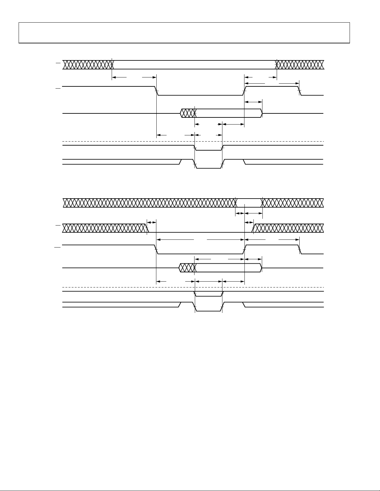
THREE-STATE TIMING—BUS MASTER, BUS SLAVE, HBR, SBTS
These specifications show how the memory interface is disabled (stops driving) or enabled (resumes driving) relative to CLKIN and the
SBTS
pin. This timing is applicable to bus master transition cycles (BTC) and host transition cycles (HTC) as well as the
Table 14. Specifications
5 V 3.3 V
Parameter
Timing Requirements:
t
STSCK
t
HTSCK
SBTS Setup before CLKIN
SBTS Hold before CLKIN
Switching Characteristics:
t
MIENA
t
MIENS
t
MIENHG
t
MITRA
t
MITRS
t
MITRHG
t
DATEN
t
DATTR
t
ACKEN
t
ACKTR
t
ADCEN
t
ADCTR
t
MTRHBG
t
MENHBG
Address/Select Enable after CLKIN −1.5 − DT/8 −1.25 − DT/8 ns
Strobes Enable after CLKIN
HBG Enable after CLKIN
Address/Select Disable after CLKIN 1 − DT/4 1.25 − DT/4 ns
Strobes Disable after CLKIN1 2.5 − DT/4 2.5 − DT/4 ns
HBG Disable after CLKIN
Data Enable after CLKIN
Data Disable after CLKIN2 0 − DT/8 8 − DT/8 0 − DT/8 8 − DT/8 ns
ACK Enable after CLKIN2 7.5 + DT/4 7.5 + DT/4 ns
ACK Disable after CLKIN2 −1 − DT/8 +7 − DT/8 −1 − DT/8 +7 − DT/8 ns
ADRCLK Enable after CLKIN −2 − DT/8 −2 − DT/8 ns
ADRCLK Disable after CLKIN 9 − DT/4 9 − DT/4 ns
Memory Interface Disable before HBG Low
Memory Interface Enable after HBG High3
1
2
3
Min Max Min Max
12.5 + DT/2 12.5 + DT/2 ns
5.5 + DT/2 5.5 + DT/2 ns
−1.5 − DT/8 −1.5 − DT/8 ns
−1.5 − DT/8 −1.5 − DT/8 ns
3 − DT/4 3 − DT/4 ns
9 + 5 DT/16 9 + 5 DT/16 ns
−1 + DT/8 −1 + DT/8 ns
18.5 + DT 18.5 + DT ns
SBTS
pin.
Unit
1
Strobes = RD, WR, SW, PAGE,
2
In addition to bus master transition cycles, these specifications also apply to bus master and bus slave synchronous read/write.
3
Memory interface = address, RD, WR, MSx, SW,
DMAG
.
HBG
, PAGE,
DMAG
x,
(in EPROM boot mode).
BMS
CLKIN
t
STSCK
t
HTSCK
SBTS
t
,
t
,
MEMORY
INTERFACE
DATA
ACK
ADRCLK
HBG
MEMORY
INTERFACE
MIENA
t
DATEN
t
ACKEN
t
ADCEN
MEMORY INTERFACE
t
MIENS
MIENHG
t
ADCTR
t
MENHBG
= ADDRESS, RD, WR, MSx, SW, HBG, PAGE, DMAGx. BMS (IN EPROM BOOT MODE)
Figure 14. Three-State Timing
t
DATTR
t
ACKTR
t
MITRA
,
t
MITRS
,
t
MITRHG
t
MTRHBG
00667-023
Rev. B | Page 17 of 48

AD14060/AD14060L
DMA HANDSHAKE
These specifications describe the three DMA handshake modes. In all three modes,
DMAG
mode,
ADDR
WR, MS
read/write—bus master timing specifications for ADDR
Table 15. Specifications
Parameter
Timing Requirements:
t
SDRLC
t
SDRHC
t
WDR
t
SDATDGL
t
HDATIDG
t
DATDRH
t
DMARLL
t
DMARH
Switching Characteristics:
t
DDGL
t
WDGH
t
WDGL
t
HDGC
t
VDATDGH
t
DATRDGH
t
DGWRL
t
DGWRH
t
DGWRR
t
DGRDL
t
DRDGH
t
DGRDR
t
DGWR
t
DADGH
t
DDGHA
W = number of wait states specified in WAIT register × tCK.
, if an address hold cycle or bus idle cycle occurs, as specified in WAIT register; otherwise, HI = 0.
HI = t
CK
1
Required only for recognition in the current cycle.
2
t
SDATDGL
can be driven t
3
t
VDATDGH
equals the number of extra cycles that the access is prolonged.
4
See the section for the calculation of hold times given capacitive and dc loads. System Hold Time Calculation Example
controls the latching or enabling of data externally. For external handshake mode, the data transfer is controlled by the
, RD, WR, SW, PAGE,
31-0
, and ACK (not
3-0
MS
, ACK, and
3-0
DMAG
). For paced master mode, the memory read—bus master, memory write—bus master, and synchronous
DMAG
signals. For paced master mode, the data transfer is controlled by ADDR
, RD, WR,
31-0
MS
, SW, PAGE, DATA
3-0
5 V 3.3 V
Min Max Min Max
DMARx Low Setup before CLKIN
DMARx High Setup before CLKIN1
DMAR
x Width Low (Nonsynchronous)
Data Setup after DMAGx Low
2
Data Hold after DMAGx High
Data Valid after DMAGx High2
DMAGx Low Edge to Low Edge
DMAGx Width High
1
5 5 ns
5 5 ns
6 6 ns
9 + 5 DT/8 9 + 5 DT/8 ns
2 2 ns
15.5 + 7 DT/8 15.5 + 7 DT/8 ns
23 + 7 DT/8 23 + 7 DT/8 ns
6 6 ns
DMAGx Low Delay after CLKIN
DMAGx High Width
DMAGx Low Width
DMAGx High Delay after CLKIN
Data Valid before DMAGx High
Data Disable after DMAGx High
WR Low before DMAGx Low
DMAGx Low before WR High
WR High before DMAGx High
RD Low before DMAGx Low
RD Low before DMAGx High
RD High before DMAGx High
DMAGx High to WR, RD, DMAGx Low
Address/Select Valid to DMAGx High
Address/Select Hold after DMAGx High
is the data setup requirement, if
is valid, if
DATDRH
DMAR
after
x is brought high.
DMAR
x is not being used to hold off completion of a read. If
x is not being used to hold off completion of a write. Otherwise, if
DMAR
3
4
9 + DT/4 16 + DT/4 9 + DT/4 16 + DT/4 ns
6 + 3 DT/8 6 + 3 DT/8 ns
12 + 5 DT/8 12 + 5 DT/8 ns
−2 − DT/8 +7 − DT/8 −2 − DT/8 +7 − DT/8 ns
7.5 + 9 DT/16 7.5 + 9 DT/16 ns
−1 +7.5 −1 +7.5 ns
−0.5 +2.5 −0.75 +2.5 ns
9.5 + 5 DT/8 + W 9.5 + 5 DT/8 + W ns
0.5 + DT/16 3.5 + DT/16 0.5 + DT/16 3.5 + DT/16 ns
−0.25 +2.5 0 2.5 ns
11 + 9 DT/16 + W 11 + 9 DT/16 + W ns
0 3.5 0 3.5 ns
4.5 + 3 DT/8 + HI 4.5 + 3 DT/8 + HI ns
16 + DT 16 + DT ns
−1.5 −1.5 ns
x is used to prolong the read, then t
DMAR
DMAR
is used to initiate transfers. For handshake
, and ACK also apply.
47-0
x low holds off completion of the write, the data
DMAR
= 7.5 + 9 DT/16 + (n × tCK), where n
VDATDGH
31-0
, RD,
Unit
Rev. B | Page 18 of 48

AD14060/AD14060L
CLKIN
t
DMARx
DMAGx
SDRLC
t
WDR
t
DMARLL
t
DDGL
t
WDGL
t
SDRHC
t
DMARH
t
HDGC
t
WDGH
TRANSFERS BETWEEN ADSP-2106x INTERNAL MEMORY AND EXTERNAL DEVICE
EXTERNAL DRIVE)
EXTERNAL DRIVE
TRANSFERS BETWEEN EXTERNAL DEVICE AND EXTERNAL MEMORY1 (EXTERNAL HANDSHAKE MODE)
(EXTERNAL DEVICE TO
EXTERNAL MEMORY)
(EXTERNAL MEMORY
TO EXTERNAL DEVICE)
DATA (FROM
ADSP-2106x TO
t
DATDRH
t
t
DADGH
SDATDGL
t
DGWRH
t
DRDGH
DATA (FROM
TO ADSP-2106x)
t
WR
RD
ADDRESS
MS
, SW
X
1
MEMORY READ – BUS MASTER, MEMORY WRITE – BUS MASTER, AND SYNCHRONOUS READ/WRITE – BUS MASTER.
TIMING SPECIFICATIONS FOR ADDR
, RD, WR, SW, MS
31–0
DGWRL
t
DGRDL
, AND ACK ALSO APPLY HERE.
3-0
Figure 15. DMA Handshake Timing
t
VDATDGH
t
DGWRR
t
DGRDR
t
DATRDGH
t
HDATIDG
t
DDGHA
00667-024
Rev. B | Page 19 of 48

AD14060/AD14060L
Table 16. 1× CLK Speed Operation
5 V 3.3 V
Parameter
Receive
Timing Requirements:
t
SLDCL
t
HLDCL
t
LCLKIW
t
LCLKRWL
t
LCLKRWH
Data Setup before LCLK Low 3.5 3 ns
Data Hold after LCLK Low 3 3 ns
LCLK Period (1× Operation) t
LCLK Width Low 6 6 ns
LCLK Width High 5 5 ns
Switching Characteristics:
t
DLAHC
t
DLALC
t
ENDLK
t
TDLK
LACK High Delay after CLKIN High 18 + DT/2 29.5 + DT/2 18 + DT/2 30 + DT/2 ns
LACK Low Delay after LCLK High
LACK Enable from CLKIN 5 + DT/2 5 + DT/2 ns
LACK Disable from CLKIN 21 + DT/2 21 + DT/2 ns
Transmit
Timing Requirements:
t
SLACH
t
HLACH
LACK Setup before LCLK High 18 20 ns
LACK Hold after LCLK High −7 −7 ns
1
Min Max Min Max
CK
tCK ns
−3 +13.5 −3 +13.5 ns
Switching Characteristics:
t
DLCLK
t
DLDCH
t
HLDCH
t
LCLKTWL
t
LCLKTWH
t
DLACLK
LCLK Delay after CLKIN (1× Operation) 16.5 17.5 ns
Data Delay after LCLK High 3.5 3 ns
Data Hold after LCLK High −3 −3 ns
LCLK Width Low (tCK/2) − 2 (tCK/2) + 2 (tCK/2) − 1 (tCK/2) + 2.25 ns
LCLK Width High (tCK/2) − 2 (tCK/2) + 2 (tCK/2) − 2.25 (tCK/2) + 1 ns
LCLK Low Delay after LACK High (tCK/2) + 8.5 (3 × tCK/2) + 17.5 (tCK/2) + 8
(3 × t
CK
/2) +
18.25
t
ENDLK
t
TDLK
Link Port Service Request Interrupts:
LDAT, LCLK Enable after CLKIN 5 + DT/2 5 + DT/2 ns
LDAT, LCLK Disable after CLKIN 21 + DT/2 21 + DT/2 ns
1× and 2× Speed Operations
Timing Requirements:
t
t
SLCK
HLCK
LACK/LCLK Setup before CLKIN Low
LACK/LCLK Hold after CLKIN Low2 2.5 2.5 ns
2
10 10 ns
1
LACK goes low with t
2
Required only for interrupt recognition in the current cycle.
relative to the rising edge of LCLK after the first nibble is received. LACK does not go low, if the receiver’s link buffer is not about to fill.
DLALC
Unit
ns
Rev. B | Page 20 of 48

AD14060/AD14060L
Table 17. 2× CLK Speed Operation
5 V 3.3 V
Parameter
Receive
Timing Requirements:
t
SLDCL
t
HLDCL
t
LCLKIW
t
LCLKRWL
t
LCLKRWH
Data Setup before LCLK Low 2.75 2.25 ns
Data Hold after LCLK Low 2.25 2.25 ns
LCLK Period (2× Operation) tCK/2 tCK/2 ns
LCLK Width Low 4.6 5.25 ns
LCLK Width High 4.25 4.5 ns
Switching Characteristics:
t
DLAHC
t
DLALC
LACK High Delay after CLKIN High 18 + DT/2 31.5 + DT/2 18 + DT/2 30.5 + DT/2 ns
LACK Low Delay after LCLK High
Transmit
Timing Requirements:
t
SLACH
t
HLACH
LACK Setup before LCLK High 20.25 19 ns
LACK Hold after LCLK High −6.5 −6.5 ns
Switching Characteristics:
t
DLCLK
t
DLDCH
t
HLDCH
t
LCLKTWL
t
LCLKTWH
t
DLACLK
LCLK Delay after CLKIN 9 9 ns
Data Delay after LCLK High 3.25 2.75 ns
Data Hold after LCLK High −2 −2 ns
LCLK Width Low (tCK/4) − 1 (tCK/4) + 1.5 (tCK/4) − 0.75 (tCK/4) + 1.5 ns
LCLK Width High (tCK/4) − 1.5 (tCK/4) + 1 (tCK/4) − 1.5 (tCK/4) + 1 ns
LCLK Low Delay after LACK High (tCK/4) + 9 (3 × tCL/4) + 17 (tCK/4) + 9 (3 × tCL/4) + 17 ns
1
LACK goes low with t
relative to the rising edge of LCLK after the first nibble is received. LACK does not go low, if the receiver’s link buffer is not about to fill.
DLALC
Min Max Min Max
1
6 17.8 6 19 ns
Unit
Rev. B | Page 21 of 48

AD14060/AD14060L
TRANSMIT
CLKIN
t
LCLK 1x
OR
LCLK 2x
LDAT(3:0)
LACK (IN)
RECEIVE
CLKIN
LCLK 1x
OR
LCLK 2x
LDAT(3:0)
THE
DLCLK
t
LCLKTWH
t
HLDCH
OUT
t
REQUIREMENT APPLIES TO THE RISING EDGE OF LCLK ONLY FOR THE FIRST NIBBLE TRANSMITTED.
SLACH
t
DLDCH
t
LCLKTWL
t
LCLKRWH
t
SLDCL
IN
LAST NIBBLE
TRANSMITTED
t
LCLKIW
t
HLDCL
t
SLACH
t
LCLKRWL
FIRST NIBBLE
TRANSMITTED
t
HLACH
LCLK INACTIVE
(HIGH)
t
DLACLK
t
DLAHC
LACK (OUT)
LACK GOES LOW ONLY AFTER THE SECOND NIBBLE IS RECEIVED.
LINK PORT ENABLE/THREE-STATE DELAY FROM INSTRUCTION
CLKIN
t
LCLK
LDAT(3:0)
LACK
LINK PORT ENABLE OR THREE-STATE TAKES EFFECT 2 CYCLES AFTER A WRITE TO A LINK PORT CONTROL REGISTER.
ENDLK
LINK PORT INTERRUPT SETUP TIME
CLKIN
t
HLCK
LCLK
LACK
t
SLCK
t
TDLK
Figure 16. Link Ports
t
DLALC
00667-025
Rev. B | Page 22 of 48

AD14060/AD14060L
Table 18. Serial Ports
5 V 3.3 V
Parameter
External Clock
Timing Requirements:
t
SFSE
t
HFSE
t
SDRE
t
HDRE
t
SCLKW
t
SCLK
TFS/RFS Setup before TCLK/RCLK
TFS/RFS Hold after TCLK/RCLK
Receive Data Setup before RCLK1 2 2 ns
Receive Data Hold after RCLK1 4.5 4.5 ns
TCLK/RCLK Width 9.5 9.5 ns
TCLK/RCLK Period t
1
1, 2
Internal Clock
Timing Requirements:
t
t
t
t
SFSI
HFSI
SDRI
HDRI
TFS Setup before TCLK1; RFS Setup before RCLK1 9.5 9.5 ns
TFS/RFS Hold after TCLK/RCLK
1, 2
Receive Data Setup before RCLK1 4.5 4.5 ns
Receive Data Hold after RCLK1 3 3 ns
External or Internal Clock
Switching Characteristics:
t
t
DFSE
HFSE
RFS Delay after RCLK (Internally Generated RFS)
RFS Hold after RCLK (Internally Generated RFS)3 2.5 2.5 ns
External Clock
Switching Characteristics:
t
t
t
t
DFSE
HFSE
DDTE
HDTE
TFS Delay after TCLK (Internally Generated TFS)3 14.5 14.5 ns
TFS Hold after TCLK (Internally Generated TFS)3 3 3 ns
Transmit Data Delay after TCLK3 17.5 17.5 ns
Transmit Data Hold after TCLK3 5 5 ns
Internal Clock
Switching Characteristics:
t
DFSI
t
HFSI
t
DDTI
t
HDTI
t
SCLKIW
TFS Delay after TCLK (Internally Generated TFS)3 5 5 ns
TFS Hold after TCLK (Internally Generated TFS)3 −1.5 −1.5 ns
Transmit Data Delay after TCLK3 7.5 7.5 ns
Transmit Data Hold after TCLK3 −0.5 −0.5 ns
TCLK/RCLK Width (SCLK/2) − 2 (SCLK/2) + 2 (SCLK/2) − 2.5 (SCLK/2) + 2.5 ns
Enable and Three-State
Switching Characteristics:
t
DDTEN
t
DDTTE
t
DDTIN
t
DDTTI
t
DCLK
t
DPTR
Data Enable from External TCLK3 3.5 4 ns
Data Disable from External TCLK3 12 12 ns
Data Enable from Internal TCLK3 −0.5 −0.5 ns
Data Disable from Internal TCLK3 3 3 ns
TCLK/RCLK Delay from CLKIN 23.5 + 3 DT/8 23.5 + 3 DT/8 ns
SPORT Disable after CLKIN 18.5 18.5 ns
Gated SCLK with External TFS (Mesh Multiprocessing)
Timing Requirements:
t
STFSCK
t
HTFSCK
TFS Setup before CLKIN 5.5 5.5 ns
TFS Hold after CLKIN (TCK/2) + 0.5 (TCK/2) + 0.5 ns
Min Max Min Max
4 4 ns
4.5 4.5 ns
CK
tCK ns
1 1 ns
3
14.5 14.5 ns
Unit
Rev. B | Page 23 of 48

AD14060/AD14060L
5 V 3.3 V
Parameter
External Late Frame Sync
Switching Characteristics:
t
DDTLFSE
t
DDTENFS
To determine whether communication is possible between two devices at clock speed n, the following specifications must be confirmed: 1) frame sync delay and frame
Data Delay from Late External TFS or External RFS
with MCE = 1, MFD = 0
4
Data Enable from Late FS or MCE = 1, MFD = 04 3.0 3.5 ns
Min Max Min Max
14.1 14.3 ns
sync setup and hold, 2) data delay and data setup and hold, and 3) SCLK width.
1
Referenced to sample edge.
2
RFS hold after RCK when MCE = 1, MFD = 0 is 0.5 ns minimum from drive edge. TFS hold after TCK for late external TFS is 0.5 ns minimum from drive edge.
3
Referenced to drive edge.
4
MCE = 1, TFS enable and TFS valid follow t
DDTLFSE
and t
DDTENFS
.
EXTERNAL RFS WITH MCE = 1, MFD = 0
t
HDTE/I
DRIVE
t
DDTE/I
t
HFSE/I
1
RCLK
RFS
DT
DRIVE SAMPLE
t
SFSE/I
t
DDTENFS
FIRST BIT SECOND BIT
t
DDTLFSE
Unit
LATE EXTERNAL TFS
t
HDTE/I
DRIVE
t
DDTE/I
t
HFSE/I
1
00667-026
DRIVE SAMPLE
TCLK
t
SFSE/I
TFS
t
DDTENFS
DT
1
RFS HOLD AFTER RCK WHEN MCE = 1, MFD = 0 IS 0.5ns MINIMUM FROM DRIVE EDGE.
TFS HOLD AFTER TCK FOR LATE EXTERNAL TFS IS 0.5ns MINIMUM FROM DRIVE EDGE.
FIRST BIT SECOND BIT
t
E
T
L
F
S
D
D
Figure 17. External Late Frame Sync
Rev. B | Page 24 of 48

AD14060/AD14060L
DATA RECEIVE– INTERNAL CLOCK
DRIVE
RCLK
RFS
EDGE
t
HFSE
t
DFSE
t
SCLKIW
t
SFSI
SAMPLE
EDGE
t
HFSI
DATA RECEIVE– EXTERNAL CLOCK
DRIVE
RCLK
RFS
EDGE
t
HFSE
t
DFSE
t
SCLKW
t
SFSE
SAMPLE
EDGE
t
HFSE
t
SDRI
DR
NOTE: EITHER THE RISING EDGE OR FALLING EDGE OF RCLK, TCLK CAN BE USED AS THE ACTIVE SAMPLING EDGE.
DATA TRANSMIT– INTERNAL CLOCK
DRIVE
TCLK
TFS
DT
EDGE
TCLK (EXT)
t
HFSI
t
HDTI
NOTE: EITHER THE RISING EDGE OR FALLING EDGE OF RCLK, TCLK CAN BE USED AS THE ACTIVE SAMPLING EDGE.
DT
t
DFSI
t
DDTI
DRIVE
EDGE
DRIVE
EDGE
t
DDTEN
t
SCLKIW
t
SFSI
SAMPLE
EDGE
t
HDRI
t
HFSI
DR
DATA TRANSMIT– EXTERNAL CLOCK
DRIVE
TCLK
TFS
DT
TCLK/RCLK
TCLK/RCLKTCLK (INT)
EDGE
t
HFSE
t
HDTE
DRIVE
EDGE
DRIVE
EDGE
t
DFSE
t
DDTE
t
DDTTE
t
SCLKW
t
SDRE
t
SFSE
SAMPLE
EDGE
t
HDRE
t
HFSE
CLKIN
TCLK, RCLK
TFS, RFS, DT
TCLK (INT)
RCLK (INT)
DT
SPORT DISABLE DELAY
FROM INSTRUCTION
t
DCLK
LOW TO HIGH ONLY
t
t
DDTIN
DPTR
SPORT ENABLE AND
THREE-STATE LATENCY
IS TWO CYCLES
Figure 18. Serial Ports
Rev. B | Page 25 of 48
t
DDTTI
CLKIN
t
STFSCK
TFS (EXT)
NOTE: APPLIES ONLY TO GATED SERIAL CLOCK MODE WITH
EXTERNAL TFS, AS USED IN THE SERIAL PORT SYSTEM I/O
FOR MESH MULTIPROCESSING.
t
HTFSCK
00667-027

AD14060/AD14060L
O
Table 19. JTAG Test Access Port and Emulation
Parameter
Timing Requirements:
t
TCK
t
STAP
t
HTAP
t
SSYS
t
HSYS
t
TRSTW
Switching Characteristics:
t
DTDO
t
DSYS
1
System Inputs = DATA
TFS1, RFS0, RFS1, LxDAT
2
System Outputs = DATA
RCLK1, TFS0, TFS1, RFS0, RFS1, LxDAT
TCK Period t
TDI, TMS Setup before TCK High 5 ns
TDI, TMS Hold after TCK High 6 6 ns
System Inputs Setup before TCK Low
System Inputs Hold after TCK Low1 18.5 19 ns
TRST Pulse Width
TDO Delay from TCK Low 13.5 13.5 ns
System Outputs Delay after TCK Low
, ADDR
47-0
3-0
47-0
, RD, WR, ACK,
31-0
, LxCLK, LxACK, EBOOT, LBOOT,
, ADDR
,
MS
31-0
, LxCLK, LxACK,
3-0
TCK
TMS
TDI
TDO
SYSTEM
INPUTS
SYSTEM
UTPUTS
SBTS, SW, HBR, HBG, CS, DMAR1, DMAR2, BR
BMS
, RD, WR, ACK, PAGE, ADRCLK, SW,
3-0
BMS
t
DTDO
Min Max Min Max
CK
1
7 8 ns
4 t
CK
2
, CLKIN,
RESET
.
HBG
, REDY,
.
t
TCK
t
STAP
t
DSYS
Figure 19. IEEE 11499.1 JTAG Test Access Port
20 20 ns
, RPBA,
6-1
DMAG1, DMAG2, BR
t
HTAP
5 V 3.3 V
Unit
tCK ns
4 t
, FLAG2-0, DR0, DR1, TCLK0, TCLK1, RCLK0, RCLK1, TFS0,
IRQ
2-0
,
CPA
6-1
t
SSYS
CK
, FLAG
, TIMEXP, DT0, DT1, TCLK0, TCLK1, RCLK0,
2-0
t
HSYS
ns
00667-028
Rev. B | Page 26 of 48

AD14060/AD14060L
ABSOLUTE MAXIMUM RATINGS
Table 20.
Parameters Ratings
Supply Voltage (5 V) −0.3 V to +7 V
Supply Voltage (3.3 V) −0.3 V to +4.6 V
Input Voltage −0.5 V to VDD + 0.5 V
Output Voltage Swing −0.5 V to VDD + 0.5 V
Load Capacitance 200 pF
Junction Temperature under Bias 130°C
Storage Temperature Range −65°C to +150°C
Lead 280°C
ESD CAUTION
ESD (electrostatic discharge) sensitive device. Electrostatic charges as high as 4000 V readily accumulate on
the human body and test equipment and can discharge without detection. Although this product features
proprietary ESD protection circuitry, permanent damage may occur on devices subjected to high energy
electrostatic discharges. Therefore, proper ESD precautions are recommended to avoid performance
degradation or loss of functionality.
Stresses greater than those listed above may cause permanent
damage to the device. These are stress ratings only; functional
operation of the device at these or any other conditions greater
than those indicated in the operational sections of this
specification is not implied. Exposure to absolute maximum
rating conditions for extended periods may affect device
reliability.
Rev. B | Page 27 of 48

AD14060/AD14060L
PIN CONFIGURATION AND FUNCTION DESCRIPTIONS
1
AD14060/AD14060L
TOP VIEW
232308
231
77
78 154
Figure 20. 308-Lead CQFP Pin Configuration
155
00667-043
Rev. B | Page 28 of 48

AD14060/AD14060L
Table 21. Pin Numbers and Mnemonics
Pin
Mnemonic
No.
1 WR 45 GND 89 ADDR13 133 IRQ
2 RD 46 RFSD1 90 ADDR12 134 IRQ
3 GND 47 RCLKD1 91 ADDR11 135 IRQ
4 CSA 48 DRD1 92 GND 136 GND 180 LC3ACK 224 LA3DAT0 268 DATA26
5 CSB 49 TFSD1 93 ADDR10 137 IRQ
6 CSC 50 TCLKD1 94 ADDR9 138 IRQ
7 CSD 51 DTD1 95 ADDR8 139 IRQ
8 GND 52 V
9 HBG 53 HBR 97 ADDR7 141 IRQ
10 REDY 54 DMAR
11 ADRCLK 55 DMAR
12 V
DD
13 RFS0 57 BMSA 101 ADDR4 145 LBOOTA 189 LC1DAT0 233 LA1DAT2 277 DATA33
14 RCLK0 58 BMSBCD 102 ADDR3 146 EBOOTBCD 190 LC1DAT1 234 LA1DAT3 278 DATA34
15 DR0 59 SW 103 ADDR2 147 LBOOTBCD 191 LC1DAT2 235 GND 279 DATA35
16 TFS0 60 GND 104 V
17 TCLK0 61 MS
18 DT0 62 MS
19 GND 63 MS
20 CPAA 64 MS
21 CPAB 65 V
22 CPAC 66 ADDR31 110 FLAGB0 154 LD4DAT0 198 LB4DAT2 242 DATA5 286 DATA40
23 CPAD 67 ADDR30 111 FLAGB2 155 LD4DAT1 199 LB4DAT3 243 DATA6 287 DATA41
24 V
DD
25 RFSA1 69 GND 113 FLAGC2 157 LD4DAT3 201 LB3ACK 245 GND 289 GND
26 RCLKA1 70 ADDR28 114 FLAGD0 158 V
27 DRA1 71 ADDR27 115 FLAGD2 159 LD3ACK 203 LB3DAT0 247 DATA9 291 DATA43
28 TFSA1 72 ADDR26 116 V
29 TCLKA1 73 V
30 DTA1 74 ADDR25 118 EMU 162 LD3DAT1 206 LB3DAT3 250 V
31 GND 75 ADDR24 119 TIMEXPA 163 LD3DAT2 207 GND 251 DATA12 295 DATA46
32 RFSB1 76 ADDR23 120 TIMEXPB 164 LD3DAT3 208 LB1ACK 252 DATA13 296 DATA47
33 RCLKB1 77 ADDR22 121 TIMEXPC 165 GND 209 LB1CLK 253 DATA14 297 GND
34 DRB1 78 ADDR21 122 TIMEXPD 166 LD1ACK 210 LB1DAT0 254 DATA15 298 BR
35 TFSB1 79 ADDR20 123 GND 167 LD1CLK 211 LB1DAT1 255 GND 299 BR
36 TCLKB1 80 V
37 DTB1 81 ADDR19 125 TRST 169 LD1DAT1 213 LB1DAT3 257 DATA17 301 BR
38 V
DD
39 RFSC1 83 ADDR17 127 TMS 171 LD1DAT3 215 LA4ACK 259 DATA19 303 BR
40 RCLKC1 84 GND 128 TCK 172 V
41 DRC1 85 ADDR16 129 V
42 TFSC1 86 ADDR15 130 IRQ
43 TCLKC1 8 ADDR14 131 IRQ
44 DTC1 88 V
Pin
No.
Mnemonic
DD
Pin
Mnemonic
No.
96 V
98 ADDR6 142
1
99 ADDR5 143 V
2
DD
Pin
Mnemonic
No.
140 IRQ
IRQ
Pin
Mnemonic
No.
B0
B1
B2
C0
C1
C2
D0
D1
D2
DD
177 LC4DAT2 221 GND 265 GND
178 LC4DAT3 222 LA3ACK 266 DATA24
179 GND 223 LA3CLK 267 DATA25
181 LC3CLK 225 LA3DAT1 269 DATA27
182 LC3DAT0 226 LA3DAT2 270 V
183 LC3DAT1 227 LA3DAT3 271 DATA28
184 LC3DAT2 228 V
185 LC3DAT3 229 LA1ACK 273 DATA30
186 V
DD
187 LC1ACK 231 LA1DAT0 275 GND
Pin
No.
Mnemonic
DD
Pin
Mnemonic
No.
DD
272 DATA29
230 LA1CLK 274 DATA31
56 SBTS 100 GND 144 EBOOTA 188 LC1CLK 232 LA1DAT1 276 DATA32
DD
0
1
2
3
DD
105 ADDR1 149
106 ADDR0 150 RPBA 194 LB4ACK 238 DATA2 282 DATA37
107 FLAGA0 151 GND 195 LB4CLK 239 DATA3 283 DATA38
108 GND 152 LD4ACK 196 LB4DAT0 240 V
109 FLAGA2 153 LD4CLK 197 LB4DAT1 241 DATA4 285 GND
68 ADDR29 112 FLAGC0 156 LD4DAT2 200 V
DD
DD
117 FLAG1 161 LD3DAT0 205 LB3DAT2 249 DATA11 293 DATA44
148 GND 192 LC1DAT3 236 DATA0 280 V
RESET 193 GND 237 DATA1 281 DATA36
DD
DD
DD
202 LB3CLK 246 DATA8 290 DATA42
244 DATA7 288 CLKIN
284 DATA39
160 LD3CLK 204 LB3DAT1 248 DATA10 292 V
DD
294 DATA45
DD
DD
1
2
DD
124 TDO 168 LD1DAT0 212 LB1DAT2 256 DATA16 300 BR
3
4
82 ADDR18 126 TDI 170 LD1DAT2 214 V
DD
258 DATA18 302 BR
5
6
DD
DD
A0
A1
DD
132 IRQ
A2
173 LC4ACK 217 LA4DAT0 261 DATA20 305 V
174 LC4CLK 218 LA4DAT1 262 DATA21 306
175 LC4DAT0 219 LA4DAT2 263 DATA22 307
176 LC4DAT1 220 LA4DAT3 264 DATA23 308 ACK
216 LA4CLK 260 V
DD
304 PAGE
DD
DMAG
1
DMAG
2
Rev. B | Page 29 of 48

AD14060/AD14060L
PIN FUNCTION DESCRIPTIONS
AD14060/AD14060L pin function descriptions are listed in
Table 22. Inputs identified as synchronous (S) must meet timing
requirements with respect to CLKIN (or with respect to TCK
for TMS, TDI). Inputs identified as asynchronous (A) can be
TRST
asserted asynchronously to CLKIN (or to TCK for
).
Unused inputs should be tied or pulled to V
for ADDR
, DATA
31-0
47-0
, FLAG
, SW, and inputs that have
2-0
internal pull-up or pull-down resistors (CPA, ACK, DTx, DRx,
TCLKx, RCLKx, LxDAT
, LxCLK, LxACK, TMS, and TDI)—
3-0
these pins can be left floating. These pins have a logic-level hold
circuit that prevents the input from floating internally.
Table 22. Pin Function Descriptions
Pin Type1Function
ADDR
31-0
I/O/T
External Bus Address (common to all SHARCs). The AD14060/AD14060L outputs addresses for external memory
and peripherals on these pins. In a multiprocessor system, the bus master outputs addresses for read/writes on the
internal memory or IOP registers of slave ADSP-2106xs. The AD14060/AD14060L inputs addresses when a host
processor or multiprocessing bus master is reading or writing the internal memory or IOP registers of internal
ADSP-21060s.
DATA
47-0
I/O/T
External Bus Data (common to all SHARCs). The AD14060/AD14060L inputs and outputs data and instructions on
these pins. 32-bit single-precision floating-point data and 32-bit fixed-point data is transferred over Bits 47–16 of
the bus. 40-bit extended-precision floating-point data is transferred over Bits 47–48 of the bus. 16-bit short word
data is transferred over Bits 31–16 of the bus. In PROM boot mode, 8-bit data is transferred over Bits 23–16. Pull-up
resistors on unused DATA pins are not necessary.
MS
3-0
O/T
Memory Select Lines (common to all SHARCs). These lines are asserted (low) as chip selects for the corresponding
banks of external memory. Memory bank size must be defined in the individual ADSP-21060’s system control
MS
registers (SYSCON). The
address lines. When no external memory access is occurring, the
lines are decoded memory address lines that change at the same time as the other
3-0
MS
lines are inactive. They are active, however,
3-0
when a conditional memory access instruction is executed, whether or not the condition is true.
with the PAGE signal to implement a bank of DRAM memory (Bank 0). In a multiprocessing system, the
are output by the bus master.
RD
I/O/T
Memory Read Strobe (common to all SHARCs). This pin is asserted (low) when the AD14060/AD14060L reads from
external devices or when the internal memory of internal ADSP-2106xs is being accessed. External devices
RD to read from the AD14060/AD14060L’s internal memory. In a
WR
I/O/T
(including other ADSP-2106xs) must assert
multiprocessing system,
RD is output by the bus master and is input by all other ADSP-2106xs.
Memory Write Strobe (common to all SHARCs). This pin is asserted (low) when the AD14060/AD14060L writes to
external devices or when the internal memory of internal ADSP-2106xs is being accessed. External devices
(including other ADSP-2106xs) must assert
multiprocessing system,
PAGE O/T
DRAM Page Boundary. The AD14060/AD16060L asserts this pin to signal that an external DRAM page boundary has
WR is output by the bus master and is input by all other ADSP-2106xs.
WR to write to the AD14060/ AD14060L’s internal memory. In a
been crossed. DRAM page size must be defined in the individual ADSP-21060’s memory control register (WAIT).
DRAM can be implemented only in external memory Bank 0. The PAGE signal can be activated only for Bank 0
accesses. In a multiprocessing system, PAGE is output by the bus master.
ADRCLK O/T Clock Output Reference (common to all SHARCs). In a multiprocessing system, ADRCLK is output by the bus master.
SW
I/O/T
Synchronous Write Select (common to all SHARCs). This signal is used to interface the AD14060/AD14060L to
synchronous memory devices (including other ADSP-2106xs). The AD14060/AD14060L asserts
an early indication of an impending write cycle, which can be aborted, if
conditional write instruction). In a multiprocessing system,
SW is output by the bus master and is input by all other
ADSP-2106xs to determine if the multiprocessor memory access is a read or write.
WR is not later asserted (for example, in a
SW is asserted at the same time
as the address output. A host processor using synchronous writes must assert this pin when writing to the
AD14060/AD14060L.
ACK I/O/S
Memory Acknowledge (common to all SHARCs). External devices can de-assert ACK (low) to add wait states to an
external memory access. ACK is used by I/O devices, memory controllers, or other peripherals to hold off completion of an external memory access. The AD14060/AD14060L de-asserts ACK, as an output, to add wait states to a
synchronous access of its internal memory. In a multiprocessing system, a slave ADSP-2106x de-asserts the bus
master’s ACK input to add wait state(s) to an access of its internal memory. The bus master has a keeper latch on its
ACK pin that maintains the input at the level to which it was last driven.
or GND, except
DD
MS0 can be used
MS
lines
3-0
SW (low) to provide
Rev. B | Page 30 of 48

AD14060/AD14060L
Pin Type1Function
SBTS
I/S
HBR
HBG
CSA
CSB
CSC
CSD
REDY
I/A
I/O
I/A Chip Select. Asserted by host processor to select SHARC_A.
I/A Chip Select. Asserted by host processor to select SHARC_B.
I/A Chip Select. Asserted by host processor to select SHARC_C.
I/A Chip Select. Asserted by host processor to select SHARC_D.
O
(O/D)
BR
6-1
I/O/S
RPBA I/S
CPAy (O/D)
I/O
DT0 O/T Data Transmit (common Serial Ports 0 to all SHARCs, TDM). The DT pin has a 50 kΩ internal pull-up resistor.
DR0 I Data Receive (common Serial Ports 0 to all SHARCs, TDM). The DR pin has a 50 kΩ internal pull-up resistor.
TCLK0 I/O Transmit Clock (common Serial Ports 0 to all SHARCs, TDM). The TCLK pin has a 50 kΩ internal pull-up resistor.
RCLK0 I/O Receive Clock (common Serial Ports 0 to all SHARCs, TDM). The RCLK pin has a 50 kΩ internal pull-up resistor.
TFS0 I/O Transmit Frame Sync (common Serial Ports 0 to all SHARCs, TDM).
RFS0 I/O Receive Frame Sync (common Serial Ports 0 to all SHARCs, TDM).
DTy1 O/T
DRy1 I
TCLKy1 I/O
RCLKy1 I/O
TFSy1 I/O Transmit Frame Sync (Serial Port 1 individual from SHARC_A, SHARC_B, SHARC_C, SHARC_D).
RFSy1 I/O Receive Frame Sync (Serial Port 1 individual from SHARC_A, SHARC_B, SHARC_C, SHARC_D).
FLAGy0 I/O/A
Suspend Bus Three-State (common to all SHARCs). External devices can assert
SBTS (low) to place the external bus
address, data, selects, and strobes in a high impedance state for the following cycle. If the AD14060/AD14060L
attempts to access external memory while
complete until
SBTS is de-asserted. SBTS should be used only to recover from host processor/AD14060/AD14060L
SBTS is asserted, the processor halts and the memory access does not
deadlock, or used with a DRAM controller.
Host Bus Request (common to all SHARCs). Must be asserted by a host processor to request control of the
AD14060/AD14060L’s external bus. When
master relinquishes the bus and asserts
and strobe lines in a high impedance state.
HBR is asserted in a multiprocessing system, the ADSP-2106x that is bus
HBG. To relinquish the bus, the ADSP-2106x places the address, data, select,
HBR has priority over all ADSP-2106x bus requests (BR
6-1
) in a
multiprocessing system.
Host Bus Grant (common to all SHARCs). Acknowledges an
take control of the external bus.
multiprocessing system,
HBG is asserted (held low) by the AD14060/AD14060L until HBR is released. In a
HBG is output by the ADSP-2106x bus master and is monitored by all others.
HBR bus request, indicating that the host processor can
Host Bus Acknowledge (common to all SHARCs). The AD14060/AD14060L de-asserts REDY (low) to add wait states
to an asynchronous access of its internal memory or IOP registers by a host. Open-drain output (O/D) by default;
can be programmed in ADREDY bit of SYSCON register of individual ADSP-21060s to be active drive (A/D). REDY is
output only if the CS and
HBR inputs are asserted.
Multiprocessing Bus Requests (common to all SHARCs). Used by multiprocessing ADSP-2106xs to arbitrate for bus
mastership. An ADSP-2106x drives only its own
monitors all others. In a multiprocessor system with less than six ADSP-2106xs, the unused
pulled high;
BR
must not be pulled high or low, because they are outputs.
4-1
BRx line (corresponding to the value of its ID2-0 inputs) and
BRx pins should be
Rotating Priority Bus Arbitration Select (common to all SHARCs). When RPBA is high, rotating priority for multiprocessor bus arbitration is selected. When RPBA is low, fixed priority is selected. This signal is a system
configuration selection that must be set to the same value on every ADSP-2106x. If the value of RPBA is changed
during system operation, it must be changed in the same CLKIN cycle on every ADSP-2106x.
Core Priority Access (y = SHARC_A, B, C, D). Asserting its CPA pin allows the core processor of an ADSP-2106x bus
slave to interrupt background DMA transfers and gain access to the external bus.
is connected to all ADSP-2106xs in the system, if this function is required. The
is brought out individually. The
a system, the
CPA pin should be left unconnected.
CPA pin has an internal 5 kΩ pull-up resistor. If core access priority is not required in
CPA is an open-drain output that
CPA pin of each internal ADSP-21060
Data Transmit (Serial Port 1 individual from SHARC_A, SHARC_B, SHARC_C, SHARC_D). The DT pin has a 50 kΩ
internal pull-up resistor.
Data Receive (Serial Port 1 individual from SHARC_A, SHARC_B, SHARC_C, SHARC_D). The DR pin has a 50 kΩ
internal pull-up resistor.
Transmit Clock (Serial Port 1 individual from SHARC_A, SHARC_B, SHARC_C, SHARC_D). The TCLK pin has a 50 kΩ
internal pull-up resistor.
Receive Clock (Serial Port 1 individual from SHARC_A, SHARC_B, SHARC_C, SHARC_D). The RCLK pin has a 50 kΩ
internal pull-up resistor.
Flag Pins (FLAG0 individual from SHARC_A, SHARC_B, SHARC_C, SHARC_D). Each pin is configured via control bits
as either an input or an output. As an input, it can be tested as a condition. As an output, it can be used to signal
external peripherals.
Rev. B | Page 31 of 48

AD14060/AD14060L
Pin Type1Function
FLAG1 I/O/A
FLAGy2 I/O/A
IRQy2-0
DMAR1
DMAR2
DMAG1
DMAG2
I/A
I/A DMA Request 1 (DMA Channel 7). Common to SHARC_A, SHARC_B, SHARC_C, SHARC_D.
I/A DMA Request 2 (DMA Channel 8). Common to SHARC_A, SHARC_B, SHARC_C, SHARC_D.
O/T DMA Grant 1 (DMA Channel 7). Common to SHARC_A, SHARC_B, SHARC_C, SHARC_D.
O/T DMA Grant 2 (DMA Channel 8). Common to SHARC_A, SHARC_B, SHARC_C, SHARC_D.
LyxCLK I/O
LyxDAT3-0 I/O
LyxACK I/O
EBOOTA I
LBOOTA I
BMSA
I/O/T
EBOOTBCD I
LBOOTBCD I
BMSBCD
I/O/T3
1 0 Output
0 0 1 (Input) Host processor.
0 1 1 (Input) Link port.
0 0 0 (Input) No booting. Processor executes from external memory.
0 1 0 (Input) Reserved.
1 1 x (Input) Reserved.
TIMEXPy O
CLKIN I
RESET
I/A
TCK I Test Clock (JTAG) (common to all SHARCs). Provides an asynchronous clock for JTAG boundary scan.
TMS I/S
Flag Pins (FLAG1 common to all SHARCs). This pin is configured via control bits internal to individual ADSP-21060s
as either an input or an output. As an input, it can be tested as a condition. As an output, it can be used to signal
external peripherals.
Flag Pins (FLAG2 individual from SHARC_A, SHARC_B, SHARC_C, SHARC_D). Each pin is configured via control bits
as either an input or an output. As an input, it can be tested as a condition. As an output, it can be used to signal
external peripherals.
Interrupt Request Lines (individual IRQ
from y = SHARC_A, SHARC_B, SHARC_C, SHARC_D). Can be either edge-
2-0
triggered or level-sensitive.
2
Link Port Clock (y = SHARC_A, B, C, D; x = Link Ports 1, 3, 4)
. Each LyxCLK pin has a 50 kΩ internal pull-down resistor
that is enabled or disabled by the LPDRD bit of the LCOM register of the ADSP-20160.
2
Link Port Data (y = SHARC_A, B, C, D; x = Link Ports 1, 3, 4)
. Each LyxDAT pin has a 50 kΩ internal pull-down resistor
that is enabled or disabled by the LPDRD bit of the LCOM register of the ADSP-21060.
2
Link Port Acknowledge (y = SHARC_A, B, C, D; x = Link Ports 1, 3, 4)
. Each LyxACK pin has a 50 kΩ internal pull-
down resistor that is enabled or disabled by the LPDRD bit of the LCOM register of the ADSP-21060.
EPROM Boot Select (SHARC_A). When EBOOTA is high, SHARC_A is configured for booting from an 8-bit EPROM.
When EBOOTA is low, the LBOOTA and
BMSA inputs determine booting mode for SHARC_A. See the following
table. This signal is a system configuration selection that should be hardwired.
Link Boot. When LBOOTA is high, SHARC_A is configured for link port booting. When LBOOTA is low, SHARC_A is
configured for host processor booting or no booting. See the following table. This signal is a system configuration
selection that should be hardwired.
3
Boot Memory Select. When this pin is an output, it is used as chip select for boot EPROM devices (when EBOOTA =
1, LBOOTA = 0). In a multiprocessor system,
BMS is output by the bus master. As an input, when low, this pin
indicates that no booting is to occur and that SHARC_A is to begin executing instructions from external memory.
See the following table. This input is a system configuration selection that should be hardwired.
EPROM Boot Select (common to SHARC_B, SHARC_C, SHARC_D). When EBOOTBCD is high, SHARC_B, C, and D are
configured for booting from an 8-bit EPROM. When EBOOTBCD is low, the LBOOTBCD and
BMSBCD inputs
determine booting mode for SHARC_B, C, and D. See the following table. This signal is a system configuration
selection that should be hardwired.
LINK Boot (common to SHARC_B, SHARC_C, SHARC_D). When LBOOTBCD is high, SHARC_B, C, and D are configured
for link port booting. When LBOOTBCD is low, SHARC_B, C, and D are configured for host processor booting or no
booting. See the following table. This signal is a system configuration selection that should be hardwired.
Boot Memory Select. When this pin is an output, it is used as chip select for boot EPROM devices (when EBOOTBCD
= 1, LBOOTBCD = 0). In a multiprocessor system,
BMS is output by the bus master. As an input, when low, this pin
indicates that no booting is to occur and that SHARC_B, C, and D are to begin executing instructions from external
memory. See table below. This input is a system configuration selection that should be hardwired.
EBOOT LBOOT
BMS
Booting Mode
EPROM (connect
BMS to EPROM chip select).
Timer Expired (individual TIMEXP from y = SHARC_A, SHARC_B, SHARC_C, SHARC_D). Asserted for four cycles when
the timer is enabled and TCOUNT decrements to 0.
Clock In (common to all SHARCs). External clock input to the AD14060/AD14060L. The instruction cycle rate is equal
to CLKIN. CLKIN cannot be halted, changed, or operated below the minimum specified frequency.
Module Reset (common to all SHARCs). Resets the AD14060/AD14060L to a known state. This input must be
asserted (low) at power-up.
Test Mode Select (JTAG) (common to all SHARCs). Used to control the test state machine. TMS has a 20 kΩ internal
pull-up resistor.
Rev. B | Page 32 of 48

AD14060/AD14060L
Pin Type1Function
TDI I/S
TDO O Test Data Output (JTAG). Serial scan output of the boundary scan chain path, from SHARC_D.
TRST
EMU (O/D)
V
DD
I/A
O
P Power Supply. Nominally 5.0 V dc for 5 V devices or 3.3 V dc for 3.3 V devices (26 pins).
GND G Power Supply Return (28 pins).
FLAG3 is connected internally, common to SHARC_A, B, C, and D.
ID pins are hardwired internally as shown in Figure 1.
1
I = input; P = power supply; (A/D) = active drive; O = output; S = synchronous; (O/D) = open drain; G = ground; A = asynchronous; T = three-state, when
asserted, or when the AD14060/AD14060L is a bus slave.
2
Link Ports 0, 2, and 5 are connected internally, as described in the Li section. nk Port I/O
3
Three-statable only in EPROM boot mode (when
Test Data Input (JTAG). Provides serial data for the boundary scan logic chain starting at SHARC_A. TDI has a 20 kΩ
internal pull-up resistor.
Test Reset (JTAG) (common to all SHARCs). Resets the test state machine.
power-up or held low for proper operation of the AD14060/AD14060L.
TRST must be asserted (pulsed low) after
TRST has a 20 kΩ internal pull-up resistor.
Emulation Status (common to all SHARCs). Must be connected to the ADSP-2106x EZ-ICE target board connector
only.
is
SBTS
is an output).
BMS
Rev. B | Page 33 of 48

AD14060/AD14060L
DETAILED DESCRIPTION
ARCHITECTURAL FEATURES
ADSP-21060 Core
The AD14060/AD14060L is based on the powerful
ADSP-21060 (SHARC) DSP chip. The ADSP-21060 SHARC
combines a high performance floating-point DSP core with
integrated, on-chip system features, including a 4-Mbit SRAM
memory, host processor interface, DMA controller, serial ports,
and both link port and parallel bus connectivity for glueless
DSP multiprocessing (see Figure 21). It is fabricated in a high
speed, low power CMOS process, and has a 25 ns instruction
cycle time. The arithmetic/logic unit (ALU), multiplier, and
shifter all perform single-cycle instructions, and the three units
are arranged in parallel, maximizing computational throughput.
SHARED MEMORY MULTIPROCESSING
The AD14060/AD14060L takes advantage of the powerful
multiprocessing features built into the SHARC. The SHARCs
are connected to maximize the performance of this cluster-offour architecture, and still allow for off-module expansion. The
AD14060/AD14060L in itself is a complete shared memory
multiprocessing system, as shown in Figure 22. The unified
address space of the SHARCs allows direct interprocessor
accesses of each SHARCs’ internal memory. In other words,
each SHARC can directly access the internal memory and IOP
registers of each of the other SHARCs by simply reading or
writing to the appropriate address in multiprocessor memory
space (see Figure 23)—this is called a direct read or direct write.
The SHARC features an enhanced Harvard architecture, in
which the data memory (DM) bus transfers data and the
program memory (PM) bus transfers both instructions and
data. An on-chip instruction cache selectively caches only those
instructions whose fetches conflict with the PM bus data
accesses. This combines with the separate program and data
memory buses to enable 3-bus operation for fetching an
instruction and two operands, all in a single cycle. The SHARC
also contains a general-purpose data register file, which is a
10-port, 32-register (16 primary, 16 secondary) file. Each
SHARC’s core also implements two data address generators
(DAGs), implementing circular data buffers in hardware. The
DAGs contain sufficient registers to allow the creation of up to
32 circular buffers. The 48-bit instruction word accommodates
a variety of parallel operations for concise programming. For
example, the ADSP-21060 can conditionally execute a multiply,
an add, a subtract, and a branch, all in a single instruction.
The SHARCs contain 4 Mbits of on-chip SRAM each, organized
as two blocks of 2 Mbits, which can be configured for different
combinations of code and data storage. The memory can be
configured as a maximum of 128k words of 32-bit data, 256k
words of 16-bit data, 80k words of 48-bit instructions (or 40-bit
data), or combinations of different word sizes up to 4 Mbits. A
16-bit floating-point storage format is supported, which
effectively doubles the amount of data that can be stored onchip. Conversion between the 32-bit floating-point and 16-bit
floating-point formats is done in a single instruction. Each
memory block is dual-ported for single-cycle, independent
access by the core processor and I/O processor or DMA
controller. The dual-ported memory and separate on-chip buses
allow two data transfers from the core and one from the I/O, all
in a single cycle.
Bus arbitration is accomplished with the on-SHARC arbitration
logic. Each SHARC has a unique ID, and drives the bus-request
(BR) line corresponding to its ID, while monitoring all others.
BR
1 to BR4 are used within the AD14060/AD14060L, while
BR
5 andBR6 can be used for expansion. All bus requests (BR1
BR
6) are included in the module I/O. Two different priority
to
schemes, fixed and rotating, are available to resolve competing
bus requests. The RPBA pin selects which scheme is used. When
RPBA is high, rotating priority bus arbitration is selected; when
RPBA is low, fixed priority is selected.
Bus mastership is passed from one SHARC to another during a
bus transition cycle. A bus transition cycle occurs only when the
current bus master de-asserts its BR line and one of the slave
SHARCs asserts its BR line. The bus master can, therefore,
retain bus mastership by keeping its BR line asserted. When the
bus master de-asserts its BR line and no other BR line is
asserted, then the master does not lose any bus cycles. When
more than one SHARC asserts its BR line, the SHARC with the
highest priority request becomes bus master on the following
cycle. Each SHARC observes all the BR lines, and, therefore,
tracks when a bus transition cycle has occurred, and which
processor has become the new bus master. Master processor
changeover incurs only one cycle of overhead. Table 23 shows
an example of a bus transition sequence.
Table 23. Rotating Priority Arbitration Example
Hardware Processor IDs
Cycle ID1 ID2 ID3 ID4 ID5 ID6 Priority
1 M 1 2 BR 3 4 5 Initial priority
2 4 5 BR M-BR 1 2 3
3 4 5 BR M 1 2 3
4 5 BR M 1 2 3 4 BR
5 1 BR 2 3 4 5 M Final priority
1–5 = Assigned priority.
M = Bus mastership (in that cycle).
BR = Requesting bus mastership with
BR
x.
assignments
assignments
Rev. B | Page 34 of 48

AD14060/AD14060L
DUAL-PORTED SRAM
TWO INDEPENDENT
DUAL-PORTED BLOCKS
DATAADDR DATA ADDR
DATAADDR DATA ADDR
IOD
48
IOP
REGISTERS
(MEMORY MAPPED)
CONTROL,
STATUS, AND
DATA BUFFERS
I/O PROCESSOR
BLOCK 0
IOA
17
DMA
CONTROLLER
SERIAL PORTS
(2)
LINK PORTS
(6)
BLOCK 1
EXTERNAL
MULTIPROCESSOR
INTERFACE
HOST PORT
JTAG
TEST AND
EMULATION
PORT
ADDR BUS
MUX
DATA BUS
MUX
4
6
6
36
7
32
48
00667-003
DAG1
8 x 4 x 32
BUS
CONNECT
(PX)
MULTIPLIER
CORE PROCESSOR
TIMER
DAG2
8 x 4 x 24
PM ADDRESS BUS
DM ADDRESS BUS
PM DATA BUS
DM DATA BUS
DATA
REGISTER
FILE
16 x 40-BIT
BARREL
SHIFTER
INSTRUCTION
CACHE
32 x 48-BIT
PROGRAM
SEQUENCER
40/32
24
32
48
ALU
PROCESSOR PORT I/O PORT
Figure 21. ADSP-21060 Processor Block Diagram (Core of AD10460)
SYSTEM EXPANSION
1× CLOCK
CLKIN
RESET
RPBA
CPA
BOOTSELECT A
BOOTSELECT BCD
DMAR1, 2
DMAG1, 2
SPORT0
FLAG1
JTAG
SHARC_A
LINKS 1, 3, AND 4;
IRQ
;
2–0
FLAGS 2 AND 0;
TIMEXP,
SPORT1
AD14060/AD14060L
(QUAD PROCESSOR CLUSTER)
SHARC_D
LINKS 1, 3, AND 4;
IRQ
;
2–0
FLAGS 2 AND 0;
TIMEXP,
SPORT1
Figure 22. Complete Shared Memory Multiprocessing System
SHARC_B
LINKS 1, 3, AND 4;
IRQ
;
2–0
FLAGS 2 AND 0;
TIMEXP,
SPORT1
SHARC_C
LINKS 1, 3, AND 4;
IRQ
;
2–0
FLAGS 2 AND 0;
TIMEXP,
SPORT1
ADDR
DATA
MS
PAGE
SBTS
ADRCLK
REDY
BR
31–0
47–0
RD
WR
ACK
SW
CS
HBR
HBG
1–6
3-0
00667-005
Rev. B | Page 35 of 48

AD14060/AD14060L
MEMORY SPACE
MULTIPROCESSOR
MEMORY SPACE
INTERNAL
(INDIVIDUAL
SHARCs)
IOP REGISTERS
NORMAL WORD ADDRESSING
SHORT WORD ADDRESSING
INTERNAL MEMORY SPACE
OF SHARC_A
ID = 001
INTERNAL MEMORY SPACE
OF SHARC_B
INTERNAL
TO AD14060
EXTERNAL
TO AD14060
NORMAL WORD ADDRESSING: 32-BIT DATA WORDS
SHORT WORD ADDRESSING: 16-BIT DATA WORDS
ID = 010
INTERNAL MEMORY SPACE
OF SHARC_C
ID = 011
INTERNAL MEMORY SPACE
OF SHARC_D
ID = 100
INTERNAL MEMORY SPACE
OF ADSP-2106x
ID = 101
INTERNAL MEMORY SPACE
OF ADSP-2106x
ID = 110
BROADCAST WRITE
TO ALL
ADSP-2106xs
48-BIT INSTRUCTION WORDS
Figure 23. AD14060/AD14060L Memory Map
0x0000 0000
0x0002 0000
0x0004 0000
0x0008 0000
0x0010 0000
0x0018 0000
0x0020 0000
0x0028 0000
0x0030 0000
0x0038 0000
0x003F FFFF
EXTERNAL
MEMORY
SPACE
BANK 0
DRAM
(OPTIONAL)
BANK 1
BANK 2
BANK 3
NONBANKED
0x0040 0000
MS
0
MS
1
MS
2
MS
3
BANK SIZE IS
SELECTED BY
MSIZE BIT FIELD
OF SYSCON
REGISTER
0xFFFF FFFF
00667-004
Bus locking is possible, allowing indivisible read-modify-write
sequences for semaphores. In either the fixed or rotating
priority scheme, it is also possible to limit the number of cycles
that the master can use to control the bus. The AD14060/
AD14060L provides the option of using the core priority access
(CPA) mode of the SHARC. Using the CPA signal allows
external bus accesses by the core processor of a slave SHARC to
take priority over ongoing DMA transfers. Also, each SHARC
can broadcast write to all other SHARCs simultaneously,
allowing the implementation of reflective semaphores.
The bus master can communicate with slave SHARCs by
writing messages to their internal IOP registers. The MSRG0 to
MSRG7 registers are general-purpose registers that can be used
for convenient message passing, semaphores, and resource
sharing among the SHARCs. For message passing, the master
communicates with a slave by writing and/or reading any of the
eight message registers on the slave. For vector interrupts, the
master can issue a vector interrupt to a slave by writing the
address of an interrupt service routine to the slave’s VIRPT
register. This causes an immediate high priority interrupt on the
slave, which, when serviced, causes it to branch to the specified
service routine.
OFF-MODULE MEMORY AND PERIPHERALS
INTERFACE
The AD14060/AD14060L’s external port provides the interface
to off-module memory and peripherals (see Figure 24). This
port consists of the complete external port bus of the SHARC,
bused in common among the four SHARCs.
The 4-gigaword off-module address space is included in the
ADSP-14060’s unified address space. Addressing of external
memory devices is facilitated by each SHARC internally
decoding the high-order address lines to generate memorybank select signals. Separate control lines are also generated for
simplified addressing of page-mode DRAM. The AD14060/
AD14060L also supports programmable memory wait states
and external memory acknowledge controls to allow interfacing
to DRAM and peripherals with variable access, hold, and
disable time requirements.
Rev. B | Page 36 of 48

AD14060/AD14060L
AD14060/
1x
CLOCK
RESET
101
3
AD14060L
CLKIN
RESET
RPBA
CONTROL
SERIALS
LINKS
DISCRETES
ADSP-2106x #5
CLKIN
RESET
RPBA
ID
2–0
ADDR
DATA
(OPTIONAL)
ADDR
DATA
31–0
47–0
RD
WR
ACK
MS
3–0
BMS
PAGE
SBTS
SW
ADRCLK
CS
HBR
HBG
REDY
CPA
BR
2–6
BR
31–0
47–0
ADDR
DATA
OE
WE
ACK
CS
CS
ADDR
DATA
5
1
ADDR
DATA
GLOBAL
MEMORY
AND
PERIPHERALS
(OPTIONAL)
BOOT
EPROM
(OPTIONAL)
HOST
PROCESSOR
INTERFACE
(OPTIONAL)
CONTROL
CPA
1–4, 6
BR
BR
31–0
47–0
CPA
1–5
BR
5
5
5
6
00667-007
110
CLKIN
RESET
RPBA
3
ID
BR
ADSP-2106x #6
(OPTIONAL)
ADDR
DATA
2–0
CONTROL
Figure 24. Optional System Interconnections
Rev. B | Page 37 of 48

AD14060/AD14060L
LINK PORT I/O
Each individual SHARC features six 4-bit link ports that
facilitate SHARC-to-SHARC communication and external I/O
interfacing. Each link port can be configured for either 1× or 2×
operation, allowing each to transfer either four or eight bits
per cycle.
The link ports can operate independently and simultaneously,
with a maximum bandwidth of 40 MBytes/s each, or a total of
240 MBytes/s per SHARC.
The AD14060/AD14060L optimizes the link port connections
internally, and brings a total of 12 of the link ports off-module
for user-defined system connections. Internally, each SHARC
has a connection to the other three SHARCs with a dedicated
link port interface. Thus, each SHARC can directly interface
with its nearest and next-nearest neighbor. The remaining three
link ports from each SHARC are brought out independently
from each SHARC. A maximum of 480 MBytes/s link port
bandwidth is then available off of the AD14060/AD14060L.
The link port connections are shown in Figure 25.
SERIAL PORTS
The SHARC serial ports provide an inexpensive interface to a
wide variety of digital and mixed-signal peripheral devices.
Each SHARC has two serial ports. The AD14060/AD14060L
provides direct access to Serial Port 1 of each SHARC. Serial
Port 0 is bused in common to each SHARC, and brought offmodule.
The serial ports can operate at the full clock rate of the module,
providing each with a maximum data rate of 40 Mbit/s.
Independent transmit and receive functions provide more
flexible communications. Serial port data can be automatically
transferred to and from on-SHARC memory via DMA, and
each of the serial ports offers time-division-multiplexed (TDM)
multichannel mode.
The serial ports can operate with little-endian or big-endian
transmission formats, with word lengths selectable from 3 bits
to 32 bits. They offer selectable synchronization and transmit
modes as well as optional µ-law or A-law companding. Serial
port clocks and frame syncs can be internally or externally
generated.
1
3
SHARC_A SHARC_B
4
0
0
1
3
SHARC_D SHARC_C
4
Figure 25. Link Port Connections
55
2
2
2
2
55
1
3
4
0
0
1
3
4
00667-006
Link Port 4, the boot-link port, is brought off independently
from each SHARC. Individual booting is then allowed, or
chained link-port booting is possible, as described in the
Multiprocessor Link-Port Booting section.
Link port data is packed into 32-bit or 48-bit words, and can be
directly read by the SHARC core processor or DMA transferred
to on-SHARC memory.
Each link port has its own double-buffered input and output
registers. Clock/acknowledge handshaking controls link port
transfers. Transfers are programmable as either transmit or
receive.
PROGRAM BOOTING
The AD14060/AD14060L supports automatic downloading of
programs following power-up or a software reset. The SHARC
offers the following options for program booting:
• From an 8-bit EPROM
• From a host processor
• Through the link ports
• No boot
In no-boot mode, the SHARC starts executing instructions
from Address 0x0040 0004 in external memory. The boot mode
is selected by the state of the following signals:
and LBOOT.
On the AD14060/AD14060L, SHARC_A’s boot mode is separately controlled, while SHARC_B, C, and D are controlled as a
group. With this flexibility, the AD14060/AD14060L can be
configured to boot using any of the following methods.
Multiprocessor Host Booting
To boot multiple ADSP-21060 processors from a host, each
ADSP-21060 must have its EBOOT, LBOOT, and
configured for host booting: EBOOT = 0, LBOOT = 0, and
BMS
= 1. After system power-up, each ADSP-21060 is in the
BR
idle state and the
host must assert the
x bus request lines are de-asserted. The
HBR
input and boot each ADSP-21060 by
asserting its CS pin and downloading instructions.
BMS
BMS
, EB OOT,
pins
Rev. B | Page 38 of 48

AD14060/AD14060L
Multiprocessor EPROM Booting
The following methods boot the multiprocessor system from an
EPROM:
• SHARC_A is booted, which then boots the others.
The EBOOT pin on the SHARC_A must be set high for
EPROM booting. All other ADSP-21060s should be
configured for host booting (EBOOT = 0, LBOOT = 0, and
BMS
= 1), which leaves them in the idle state at startup and
allows SHARC_A to become bus master and boot itself.
Only the
select of the EPROM. When SHARC_A has finished
booting, it can boot the remaining ADSP-21060s by writing
to their external port DMA Buffer 0 (EPB0) via multiprocessor memory space.
• All ADSP-21060s boot in turn from a single EPROM.
The
together to drive the chip select pin of the EPROM. Each
ADSP-21060 can boot in turn, according to its priority.
When the last one has finished booting, it must inform the
others (which can be in the idle state) that program
execution can begin.
BMS
pin of SHARC_A is connected to the chip
BMS
signals from each ADSP-21060 can be wire-OR’ed
Multiprocessor Link-Port Booting
Booting can also be accomplished from a single source through
the link ports. Link Buffer 4 must always be used for booting. To
simultaneously boot all the ADSP-21060s, a parallel common
connection is available through Link Port 4 on each of the
processors. Or, using the daisy-chain connection that exists
between the processors’ link ports, each ADSP-21060 can boot
the next one in turn. In this case, the link assignment register
(LAR) must be programmed to configure the internal link ports
with Link Buffer 4.
Multiprocessor Booting from External Memory
If external memory contains a program after reset, then
SHARC_A should be set up for no-boot mode. It begins executing from Address 0x0040 0004 in external memory. When
booting has completed, the other ADSP-21060s can be booted
by SHARC_A, if they are set up for host booting; or they can
begin executing out of external memory, if they are set up for
no-boot mode. Multiprocessor bus arbitration allows this
booting to occur in an orderly manner.
HOST PROCESSOR INTERFACE
The AD14060/AD14060L’s host interface allows easy connection to standard microprocessor buses, both 16-bit and 32-bit,
with little additional hardware required. Asynchronous transfers
at speeds of up to the full clock rate of the module are supported. The host interface is accessed through the AD14060/
AD14060L external port and is memory-mapped into the
unified address space. Four channels of DMA are available for
the host interface; code and data transfers are accomplished
with low software overhead.
The host processor requests the AD14060/AD14060L’s external
HBR
bus with the host bus request (
ready (REDY) signals. The host can directly read and write the
internal memory of the SHARCs, and can access the DMA
channel setup and mailbox registers. Vector interrupt support is
provided for efficient execution of host commands.
), host bus grant (
HBG
), and
DIRECT MEMORY ACCESS (DMA) CONTROLLER
The SHARCs’ on-chip DMA control logic allows zero-overhead
data transfers without processor intervention. The DMA
controller operates independently and invisibly to each
SHARC’s processor core, allowing DMA operations to occur
while the core is simultaneously executing its program
instructions.
DMA transfers can occur between SHARC internal memory
and either external memory, external peripherals, or a host
processor. DMA transfers can also occur between the SHARC’s
internal memory and its serial ports or link ports. DMA
transfers between external memory and external peripheral
devices are another option. External bus packing to 16-, 32- or
48-bit words is performed during DMA transfers.
Ten channels of DMA are available on the SHARCs: two via the
link ports, four via the serial ports, and four via the processor’s
external port (for either host processor, other SHARCs,
memory, or I/O transfers). Four additional link port DMA
channels are shared with Serial Port 1 and the external port.
Programs can be downloaded to the SHARCs using DMA
transfers. Asynchronous off-module peripherals can control two
DMAR
DMA channels using DMA request/grant lines (
DMAG
1-2). Other DMA features include interrupt generation
upon completion of DMA transfers and DMA chaining for
automatic linked DMA transfers.
1-2,
Rev. B | Page 39 of 48

AD14060/AD14060L
APPLICATIONS
DEVELOPMENT TOOLS
The AD14060/AD14060L is supported with a complete set of
software and hardware development tools, including an
in-circuit emulator and development software.
Analog Devices, Inc. (ADI) uses VisualDSP++®, which is an
easy-to-use integrated software development and debugging
environment (IDDE) that efficiently manages projects from
start to finish from within a single interface.
The ADSP-21262 EZ-KIT LITE™ provides developers with a
cost-effective method for initial evaluation of the ADSP-2106x
SHARC processor architecture for applications via a USB-based
PC-hosted tool set. With this EZ-KIT LITE, users can learn
about ADI’s ADSP-2106x hardware and software development
and can quickly prototype applications.
The EZ-KIT LITE includes an ADSP-2106x processor desktop
evaluation board, along with an evaluation suite of the
VisualDSP++ development and debugging environment with
the C/C++ compiler, assembler, and linker. VisualDSP++
development and debugging software, along with the USBbased debugger interface, enables users to perform standard
debugging functions (such as read and write memory, read and
write registers, load and execute executables, set and clear
breakpoints, and single-step assembly, C, and C++ source
code).
The ADI cost-effective universal serial bus (USB)-based
emulator and high performance (HP) universal serial bus
(USB)-based emulator each provide an easy, portable, nonintrusive, target-based debugging solution for ADI JTAG
processors and DSPs. These powerful USB-based emulators
perform a wide range of emulation functions, including singlestep and full speed execution with predefined breakpoints, and
viewing and altering of register and memory contents. With the
ability to automatically detect and support multiple I/O
voltages, the USB and HP USB emulators enable users to
communicate with all the ADI JTAG processors and DSPs
using either a full speed USB 1.1 or high speed USB 2.0 port on
the host PC. Applications and data can be easily and rapidly
tested and transferred between the emulators and the separately
available VisualDSP++ development and debugging environment (sold separately).
The plug-and-play architecture of the USB allows the host
operating system to automatically detect and configure the
emulators. The USB can be connected to and disconnected
from the host without opening the PC or turning off the power
to the PC. A 3-meter cable is included to connect the emulators
to the host PC, providing abundant accessibility to hard-toreach targets.
The HP USB-based emulator supports the background
telemetry channel (BTC), a nonintrusive method for exchanging data between the host and target application without
affecting the target system's real-time characteristics. Nonintrusive in-circuit emulation is assured by the use of the processor’s
JTAG interface. The emulator does not affect target system
loading or timing.
Further details and ordering information are available on the
analog.com Web site.
In addition to the software and hardware development tools
available from Analog Devices, third parties provide a wide
range of tools supporting the SHARC processor family.
Hardware tools include SHARC PC plug-in cards, multiprocessor SHARC VME boards, and daughter card modules
with multiple SHARCs and additional memory. These modules
are based on the SHARCPAC module specification. Third-party
software tools include an Ada compiler, DSP libraries, operating
systems, and block diagram design tools.
QUAD-SHARC DEVELOPMENT BOARD
The BlackTip-MCM, AD14060 development board with
software is available from Bittware Research Systems, Inc. This
board has one AD14060 BITSI interface, and PROM and SRAM
expansion options on an ISA card. It is supported by Bittware’s
SHARC software development package. To contact Bittware,
call 1-800-848-0436.
OTHER PACKAGE DETAILS
The AD14060/AD14060L contains 16 on-module 0.018 µF
bypass capacitors. It is recommended that, in the target system ,
at least four additional capacitors of 0.018 µF value be placed
around the module, one near each of the four corners.
The top surface (lid) of the AD14060/AD14060L is electrically
connected to GND on the industrial and military grade parts.
TARGET BOARD CONNECTOR FOR EMULATOR
PROBE
The ADSP-2106x emulator uses the IEEE 1149.1 JTAG test
access port of the ADSP-2106x to monitor and control the
target board processor during emulation. The emulator probe
requires that the AD14060/AD14060L’s CLKIN (optional), TMS,
TRST
TCK,
accessible on the target system via a 14-pin connector (pin strip
header) similar to Figure 26. The emulator probe plugs directly
into this connector for chip-on-board emulation. You must add
this connector to your target board design, if you intend to use
the ADSP-2106x emulator. The length of the traces between the
connector and the AD14060/AD14060L’s JTAG pins should be
as short as possible.
, TDI, TDO,
EMU
, and GND signals be made
Rev. B | Page 40 of 48

AD14060/AD14060L
12
GND
BTDI
GND
34
56
78
910
9
11 12
13 14
TOP VIEW
(Jumpers in Place)
KEY (NO PIN)
BTMS
BTCK
BTRST
Figure 26. Target Board Connector for ADSP-2106x Emulator
EMU
CLKIN (OPTIONAL)
TMS
TCK
TRST
TDI
TDO
00667-008
The 14-pin, 2-row pin-strip header is keyed at the Pin 3 location; Pin 3 must be removed from the header. The pins must be
0.025 inch square and at least 0.20 inch in length. Pin spacing
should be 0.1 inch × 0.1 inch. Pin strip headers are available
from vendors such as 3M, McKenzie, and Samtec.
BTRST
The BTMS, BTCK,
, and BTDI signals are provided so
that the test access port can also be used for board-level testing.
When the connector is not being used for emulation, place
jumpers between the Bxxx pins and the other pins, as shown in
Figure 26. If you are not going to use the test access port for
BTRST
board testing, tie
TRST
. The
V
DD
BTRST
on the connector) or held low for proper operation of
pin must be asserted after power-up (through
to GND and tie or pull up BTCK to
the AD14060/AD14060L. None of the Bxxx pins (Pins 5, 7, 9,
11) are connected on the emulator probe.
Table 24. JTAG Signals
Signal Termination
TMS Driven through 22 Ω resistor (16 µA to 3.2 µA driver).
TCK
Driven at 10 MHz through 22 Ω resistor (16 µA to 3.2 µA
driver).
TRST Driven by open-drain driver1 (pulled up by on-chip
20 kΩ resistor).
TDI Driven by 16 µA to 3.2 µA driver.
TDO One TTL load, no termination.
CLKIN One TTL load, no termination (optional signal).
EMU 4.7 kΩ pull-up resistor, one TTL load (open-drain
output from ADSP-2106x).
______________________________________
1
is driven low until the emulator probe is turned on by the emulator
TRST
software (after the invocation command).
Connecting CLKIN to Pin 4 of the emulator header is optional.
The emulator uses CLKIN only when directed to perform
operations such as starting, stopping, and single-stepping
multiple ADSP-2106xs in a synchronous manner. If these
operations do not need to occur synchronously on the multiple
processors, tie Pin 4 of the emulator header to ground.
If synchronous multiprocessor operations are needed and
CLKIN is connected, clock skew between the AD14060/
AD14060L and the CLKIN pin on the emulator header must be
minimal. If the skew is too large, synchronous operations might
be off by one cycle between processors. For synchronous multi-
EMU
processor operation, TCK, TMS, CLKIN, and
should be
treated as critical signals in terms of skew, and should be laid
out as short as possible on the board.
If TCK, TMS, and CLKIN are driving a large number of
ADSP-2106x’s (more than eight) in the system, treat them as a
clock tree using multiple drivers to minimize skew. (See the
ADSP-2106x User’s Manual for details).
The JTAG signals are terminated on the emulator probe as
listed in Table 24.
Figure 27 shows JTAG scan path connections for the
multiprocessor system.
If synchronous multiprocessor operations are not needed
(CLKIN is not connected), use appropriate parallel termination
on TCK and TMS. Note that TDI, TDO,
not critical signals in terms of skew.
Rev. B | Page 41 of 48
EMU
, and
TRST
are

AD14060/AD14060L
SHARC_A
TDI
TDI TDO
EMULATOR
OTHERJTAG
CONTROLLER
JTAG
CONNECTOR
TCK
TMS
EMU
TRST
TDO
CLKIN
TCK
OPTIONAL
TMS
EMU
TDI TDO
TRST
SHARC_B
TCK
TMS
EMU
TDI TDO
TRST
SHARC_C
TCK
TMS
EMU
TDI TDO
TRST
SHARC_D
TCK
TMS
EMU
Figure 27. JTAG Scan Path Connections for the AD14060/AD14060L
TDI TDO TDI TDO TDI TDO
5kΩ
1
TDI TDO TDI TDO TDI TDO
TRST
JTAG DEVICE
(OPTIONAL)
TDI TDO
TCK
TMS
TRST
ADSP-2106x
#n
TDI TDO
TCK
TMS
EMU
TRST
00667-009
TDI
EMU
TCK
TMS
TRST
TDO
CLKIN
1
OPEN-DRAIN DRIVER OR EQUIVALENT, THAT IS:
5kΩ
1
Figure 28. JTAG Clock Tree for Multiple ADSP-2106x Systems
OUTPUT DRIVE CURRENTS
Figure 29 shows typical I-V characteristics for the output
drivers of the ADSP-2106x. The curves represent the current
drive capability of the output drivers as a function of output
voltage.
120
100
80
60
40
20
0
–20
–40
–60
–80
SOURCE CURRENT (mA)
–100
–120
–140
–160
Figure 29. ADSP-2106x Typical Drive Currents (V
HIGH LEVEL DRIVE
(P DEVICE)
LOW LEVEL DRIVE
(N DEVICE)
SOURCE VOLTAGE (V)
= 5 V)
DD
501234
00667-029
SYSTEM
EMU
CLKIN
00667-010
POWER DISSIPATION
Total power dissipation has two components, one due to
internal circuitry and one due to the switching of external
output drivers. Internal power dissipation is dependent on the
instruction execution sequence and the data operands involved.
Internal power dissipation is calculated as follows:
= I
P
INT
The external component of total power dissipation is caused by
the switching of output pins. Its magnitude depends on the
following:
• Number of output pins that switch during each cycle (O)
• Maximum frequency at which they can switch (f)
• Load capacitance (C)
• Vo l t age s wi n g ( V
and is calculated by
P
EXT
× V
DDIN
= O × C × V
DD
)
DD
2
× f
DD
Rev. B | Page 42 of 48

AD14060/AD14060L
C
The load capacitance should include the processor’s package
capacitance (C
). The switching frequency includes driving the
IN
load high and then back low. Address and data pins can drive
high and low at a maximum rate of 1/(2 t
can switch every cycle at a frequency of 1/t
at 1/(2 t
), but selects can switch on each cycle.
CK
). The write strobe
CK
. Selec t pins switch
CK
Example
Estimate P
with the following assumptions: a system with
EXT
one bank of external data memory RAM (32-bit);
four 128k × 8 RAM chips are used, each with a load of 10 pF;
external data memory writes occur every other cycle; a rate of
) with 50% of the pins switching; and an instruction
1/(4 t
CK
cycle rate is 40 MHz (t
The P
equation is calculated for each class of pins that can
EXT
= 25 ns) and VDD = 5.0 V.
CK
drive, as shown in Table 25.A typical power consumption can
now be calculated for these conditions by adding a typical
internal power dissipation:
= P
P
TOTAL
EXT
+ (I
Note that the conditions causing a worst-case P
from those causing a worst-case P
DDIN2
× 5.0 V)
. Maximu m P
INT
are different
EXT
cannot
INT
occur while 100% of the output pins are switching from all 1s to
all 0s. It is uncommon for an application to have 100% or even
50% of the outputs switching simultaneously.
The output disable time, t
and t
, as shown in Figure 30. The time t
DECAY
, is the difference between t
DIS
MEASURED
MEASURED
is the
interval from when the reference signal switches to when the
output voltage decays ΔV from the measured output high or
output low voltage. t
is calculated with test loads CL and IL,
DECAY
and with ΔV equal to 0.5 V.
Output Enable Time
Output pins are considered to be enabled when they have made
a transition from a high impedance state to when they start
driving. The output enable time, t
, is the interval from when a
ENA
reference signal reaches a high or low voltage level to when the
output has reached a specified high or low trip point, as shown
in the output enable/disable diagram (Figure 30). If multiple
pins (such as the data bus) are enabled, the measurement value
is that of the first pin to start driving.
System Hold Time Calculation Example
To determine the data output hold time in a particular system,
first calculate t
using the previous equation. Choose ΔV to
DECAY
be the difference between the ADSP-2106x’s output voltage and
the input threshold for the device requiring the hold time. A
typical ΔV is 0.4 V. C
is the total leakage or three-state current per data line.
and I
L
The hold time is t
is the total bus capacitance per data line,
L
plus the minimum disable time (t
DECAY
HDWD
for the write cycle).
TEST CONDITIONS
Output Disable Time
Output pins are considered to be disabled when they stop
driving, go into a high impedance state, and start to decay from
their output high or low voltage. The time for the voltage on the
bus to decay by ΔV is dependent on the capacitive load, C
the load current, I
. This decay time can be approximated by the
L
following equation:
V
∆
t
DECAY
L
=
I
L
, and
L
REFERENCE
SIGNAL
V
OH (MEASURED)
V
OL (MEASURED)
OUTPUT STOPS
t
DIS
DRIVING
t
MEASURED
V
OH (MEASURED)
V
OL (MEASURED)
t
DECAY
t
ENA
– ∆V
2.0V
+ ∆V
1.0V
OUTPUT STARTS
DRIVING
HIGH-IMPEDANCE STATE.
TEST CONDITIONS CAUSE
THIS VOLTAGE TO BE
APPROXIMATELY 1.5V
V
OH (MEASURED)
V
OL (MEASURED)
Figure 30. Output Enable/Disable
Table 25. P
Pin Type Number of Pins % Switching × C × f × V
Calculations
EXT
2
DD
= P
EXT
Address 15 50 × 55 pF × 20 MHz × 25 V = 0.206 W
MSO
WR
1 0 × 55 pF × 20 MHz × 25 V = 0.00 W
1 – × 55 pF × 40 MHz × 25 V = 0.055 W
Data 32 50 × 25 pF × 20 MHz × 25 V = 0.200 W
ADRCLK 1 – × 15 pF × 40 MHz × 25 V = 0.015 W
(5 V) = 0.476 W.
P
EXT
(3.3 V) = 0.207 W.
P
EXT
00667-030
Rev. B | Page 43 of 48

AD14060/AD14060L
Capacitive Loading
Output delays and holds are based on standard capacitive loads:
50 pF on all pins (see Figure 31). The delay and hold specifications given should be derated by a factor of 1.5 ns/50 pF for
loads other than the nominal value of 50 pF. Figure 33 and
Figure 34 show how output rise time varies with capacitance.
Figure 35 graphically shows how output delays and holds vary
with load capacitance. (Note that this graph or derating does
not apply to output disable delays; see the Output Disable Time
section.) The graphs in Figure 33, Figure 34, and Figure 35
might not be linear outside the ranges shown.
I
OL
TO OUTPUT
PIN
50pF
I
OH
Figure 31. Equivalent Device Loading for AC Measurement
(Includes All Fixtures)
INPUT OR
OUTPUT
Figure 32. Voltage Reference Levels for AC Measurements
(except Output Enable/Disable)
16.0
14.0
RISE AND FALL TIMES (ns)
12.0
10.0
8.0
6.0
4.0
(0.5V – 4.5V, 10% – 90%)
3.7
2.0
1.1
0
RISE TIME
LOAD CAPACITANCE (pF)
Figure 33. Typical Output Rise Time (10% to 90% V
vs. Load Capacitance (V
1.5V
FALL TIME
= 5 V)
DD
00667-031
1.5V1.5V
00667-032
14.7
7.4
2000 20 40 60 80 100 120 140 160 180
00667-033
)
DD
3.5
RISE AND FALL TIMES (ns)
(0.8V – 2.0V)
3.0
2.5
2.0
1.5
1.0
0.6
0.5
RISE TIME
FALL TIME
0
LOAD CAPACITANCE (pF)
2.9
1.6
2000 20 40 60 80 100 120 140 160 180
00667-034
Figure 34. Typical Output Rise Time (0.8 V to 2.0 V )
= 5 V)
DD
4.5
20025 50 75 100 125 150 175
00667-035
OUTPUT DELAY OR HOLD (ns)
NOMINAL
–0.7
–1.0
vs. Load Capacitance (V
5.0
4.0
3.0
2.0
1.0
LOAD CAPACITANCE (pF)
Figure 35. Typical Output Delay or Hold vs. Load Capacitance
at Maximum Case Temperature (V
18
16
14
12
10
8
(10% – 90%)
6
4
RISE AND FALL TIMES (ns)
2
0
Y = 0.0796X + 1.17
RISE TIME
FALL TIME
LOAD CAPACITANCE (pF)
Figure 36. Typical Output Rise Time (10% to 90% V
vs. Load Capacitance (V
DD
Y = 0.0467X + 0.55
= 3.3 V)
DD
= 5 V)
2000 20 40 60 80 100 120 140 160 180
00667-036
)
DD
Rev. B | Page 44 of 48

AD14060/AD14060L
RISE AND FALL TIMES (ns)
9
8
7
(0.8V – 2.0V)
6
5
4
3
2
1
0
Y = 0.0391X + 0.36
RISE TIME
FALL TIME
LOAD CAPACITANCE (pF)
Figure 37. Typical Output Rise Time (0.8 V to 2.0 V )
vs. Load Capacitance (V
5.0
4.0
3.0
2.0
DD
Y = 0.0329X – 1.65
Y = 0.0305X + 0.24
= 3.3 V)
Trim/form can be accomplished with a universal trim/form,
a customer-designed trim/form, or with the Analog Devices
developed tooling described as follows.
A trim/form tool specific to the AD14060/AD14060L has been
developed and is available for use by all parties at
Tintronics Industries
2122-A Metro Circle
Huntsville, AL 35801
256-650-0220
Contact Person: Tom Rice
2000 20 40 60 80 100 120 140 160 180
00667-037
The package outline and dimensions resulting from this tool are
shown in Figure 39. (Alternatively, the package can be
trimmed/formed for cavity-down placement.)
4.5
0.170
(4.318)
2.110 (53.59)
2.210 ± 0.010 (56.134 ± 0.254)
1.0
OUTPUT DELAY OR HOLD (ns)
NOMINAL
–0.7
–1.0
LOAD CAPACITANCE (pF)
20025 50 75 100 125 150 175
00667-038
Figure 38. Typical Output Delay or Hold vs. Load Capacitance
at Maximum Case Temperature (V
= 3.3 V)
DD
ASSEMBLY RECOMMENDATIONS
Socket Information
Standard sockets and carriers are available for the
AD14060/AD14060L, if needed. Socket part number
IC53-3084-262 and carrier part number ICC-308-1 are
available from Yamaichi Electronics.
Trim and Form
The AD14060/AD14060L is shipped as shown in Figure 43 with
untrimmed and unformed leads and with the nonconductive tie
bar in place. This avoids disturbance of lead spacing and
coplanarity prior to assembly. Optimally, the leads should be
trimmed, formed, and solder-dipped just prior to placement on
the board.
0.016 MIN
°
TO 8
°
0
0TO10MILS
DETAIL A
00667-039
Figure 39. Package and Lead Profile
Dimensions shown in inches and (millimeters)
Rev. B | Page 45 of 48

AD14060/AD14060L
PCB LAYOUT GUIDELINES
The drawing in Figure 40 assumes that the trim/form tooling
described previously is used. These recommendations are
provided for user convenience and are PCB layout guidelines
only, based on standard practice. PCB pad footprint geometries
and placement are illustrated.
2.260 (57.404) 4 PLACES
2.060 (52.324) 4 PLACES
1.9000 (48.26) 4 PLACES
0.015
(0.381)
THIS IS A PC BOARD COMPONENT FOOTPRINT,
NOT THE PACKAGE OUTLINE.
0.025
(0.635)
0.025 (0.635) MIN
Figure 40. PC Board Component Footprint
Dimensions shown in inches and (millimeters)
KOVAR LID
0.015 MILS
0.025 (0.635) MIN
KOVAR SEAL RING
HEIGHT = 50 MILS
Thermal Characteristics
The AD14060/AD14060L is packaged in a 308-lead ceramic
quad flatpack (CQFP). The package is optimized for thermal
conduction through the core (base of the package) down to the
mounting surface. The AD14060/AD14060L is specified for a
case temperature (T
attachment material should be such that T
θ
= 0.36°C/W
JC
). Design of the mounting surface and
CASE
is not exceeded.
CASE
Thermal Cross-Section
The following data, together with the detailed mechanical
drawings in Figure 43, allows the designer to construct simple
thermal models for further analysis within targeted systems.
The top layer of the package, where the die are mounted, is a
metal V
layer. The approximate metal area coverage from the
DD
metal planes and routing layers is estimated in Table 27. The
layers are shown in Figure 41.
Table 26. Thermal Conductivity
Material Thermal Conductivity (W/cm°C)
Ceramic 0.18
Kovar™ 0.14
Tungsten 1.78
Thermoplastic 0.03
Silicon 1.45
00667-040
Table 27. Metal Coverage per Layer
Layer % Metal (1 Mil Thick)
V
DD
88
SIG2 16
SIG3 14
GND 91
SIG4 15
SIG5 13
BASE 95
SILICON DIE
19 MILS
THERMOPLASTIC
THICKNESS 5 MILS
V
DD
SIG2
SIG3
GND
SIG4
SIG5
BASE
Figure 41. Co-Fired Packaged Profile
Rev. B | Page 46 of 48
SURFACE
CERAMIC LAYER 28 MILS
CERAMIC LAYER 6 MILS
CERAMIC LAYER 6 MILS
CERAMIC LAYER 10 MILS
CERAMIC LAYER 4 MILS
CERAMIC LAYER 10 MILS
CERAMIC LAYER 10 MILS
CERAMIC LAYER 4 MILS
CERAMIC LAYER 10 MILS
CERAMIC LAYER 4 MILS
00667-041

AD14060/AD14060L
MECHANICAL CHARACTERISTICS
Lid Deflection Analysis
Table 28. External Pressure Reduction
Δ Pressure
12 psi 10.0 mil
15 psi 11.9 mil
Mechanical Model
The following data, together with the detailed mechanical
drawings in Figure 43, allows the designer to construct simple
mechanical models for further analysis within targeted systems.
Table 29. Mechanical Properties
Material Modulas of Elasticity
Ceramic 26 × 103 kg/mm
Kovar 14.1 × 10³ kg/mm
Tungsten 35 × 103 kg/mm
Thermoplastic 279 kg/mm
Silicon 11 × 103 kg/mm
Deflection
2
2
2
2
2
0.260
0.302
0.250 0.345
0.670
4X
0.616
1.890 ± 0.005
1.810 ± 0.005
1.780 ± 0.018
0.633
0.653
4X
2.050 SQ.
ADDITIONAL INFORMATION
This data sheet provides a general overview of the AD14060/
AD14060L architecture and functionality. For detailed
information on the ADSP-2106x SHARC and the ADSP-21000
Family core architecture and instruction set, refer to the
ADSP-2106x SHARC User’s Manual.
0.0124XREF0.040 ± 0.002
Figure 42. Internal Package Dimensions
Dimensions shown in inches
00667-042
Rev. B | Page 47 of 48

AD14060/AD14060L
OUTLINE DIMENSIONS
0.350 (8.89)
0.340 (8.64)
0.330 (8.38)
2.330 (59.18)
2.300 (58.42)
2.270 (57.66)
4×
232
3.050 (77.47) MAX
3.01 (76.46)
3.00 (76.20)
2.99 (75.95)
2.062 (52.38)
2.050 (52.07)
2.038 (51.77)
TOP VIEW
2.745 (69.72)
2.730 (69.34)
2.715 (68.96)
0.015 (0.381) × 45°
155231
154
3 PLACES
0.010 (0.254)
0.008 (0.203)
0.006 (0.152)
0.025 (0.635)
BSC
78
77
0.007 (0.165)
0.005 (0.127)
0.004 (0.102)
0.160 (4.064)
MAX
0.101 (2.566)
0.092 (2.337)
0.083 (2.108)
308
0.040 (1.016) × 45°
0.035 (0.889)
MAX
1
1.895 (48.13)
1.890 (48.01)
1.885 (47.88)
Figure 43. 308-Lead Ceramic Quad Flatpack (CQFP)
(QS-308)
Dimensions shown in inches and (millimeters)
ORDERING GUIDE
Temperature
Model
Range SMD
AD14060BF-4 −40°C to +100°C N/A 40 MHz 5 V 308-Lead Ceramic Quad Flatpack (CQFP) QS-308
AD14060LBF-4 −40°C to +100°C N/A 40 MHz 3.3 V 308-Lead Ceramic Quad Flatpack (CQFP) QS-308
Instruction
Rate
Operating
Voltage Package Description
Package
Option
© 2004 Analog Devices, Inc. All rights reserved. Trademarks and
registered trademarks are the property of their respective owners.
C00667–0–12/04(B)
Rev. B | Page 48 of 48


 Loading...