Low Cost
a
FEATURES
Complete Sampling 16-Bit ADC With Reference and
Clock
50 kHz Throughput
61/2 LSB Nonlinearity
Low Noise SHA: 300 mV p-p
32-Pin Hermetic DIP
Parallel and Serial Outputs
Low Power: 900 mW
APPLICATIONS
Medical and Analytical Instrumentation
Signal Processing
Data Acquisition Systems
Professional Audio
Automatic Test Equipment (ATE)
Telecommunications
PRODUCT DESCRIPTION
The AD1380 is a complete, low cost 16-bit analog-to-digital
converter, including internal reference, clock and sample/hold
amplifier. Internal thin-film-on-silicon scaling resistors allow
analog input ranges of ±2.5 V, ±5 V, ±10 V, 0 V to +5 V and
0 V to +10 V.
Important performance characteristics of the AD1380 include
maximum linearity error of ±0.003% of FSR (AD1380KD) and
maximum 16-bit conversion time of 14 µs. Transfer characteristics of the AD1380 (gain, offset and linearity) are specified for
the combined ADC/SHA, so total performance is guaranteed as
a system. The AD1380 provides data in parallel and serial form
with corresponding clock and status outputs. All digital inputs
and outputs are TTL or 5 V CMOS compatible.
16-Bit Sampling ADC
AD1380
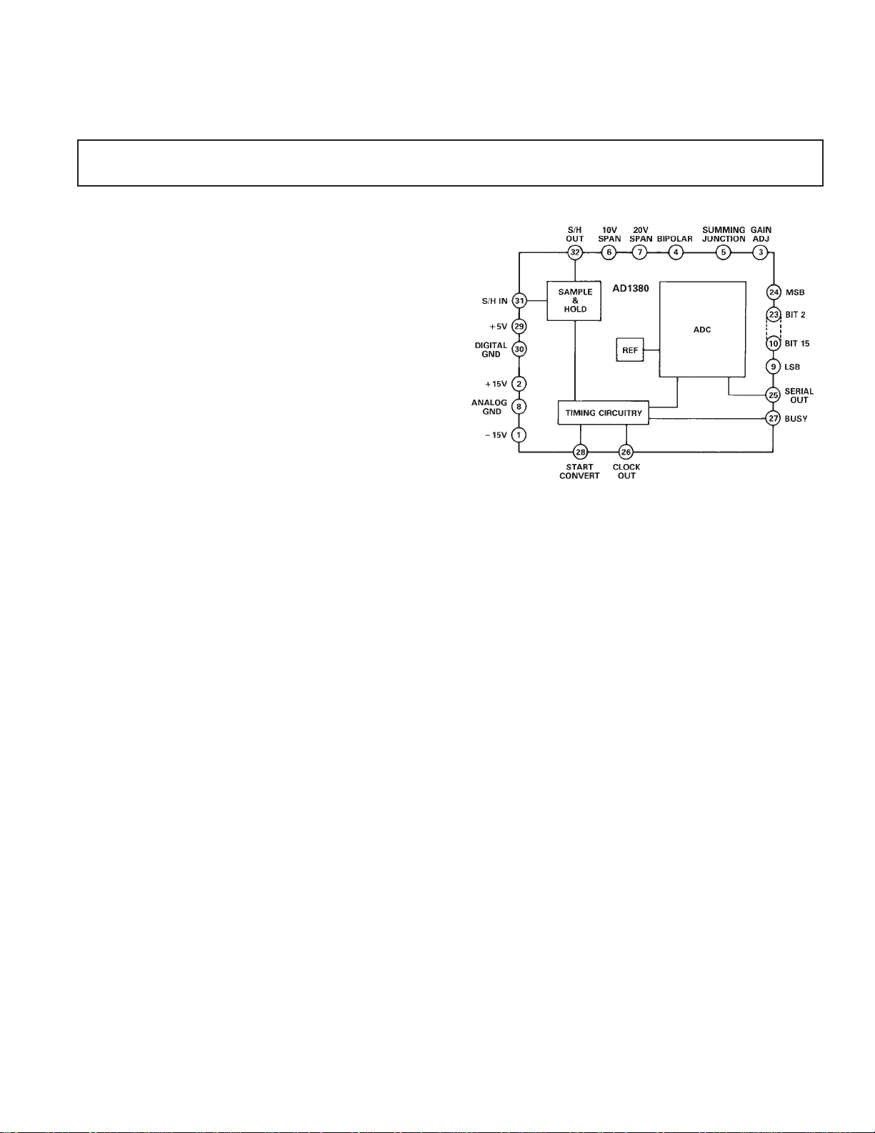
FUNCTIONAL BLOCK DIAGRAM
REV. B
Information furnished by Analog Devices is believed to be accurate and
reliable. However, no responsibility is assumed by Analog Devices for its
use, nor for any infringements of patents or other rights of third parties
which may result from its use. No license is granted by implication or
otherwise under any patent or patent rights of Analog Devices.
One Technology Way, P.O. Box 9106, Norwood, MA 02062-9106, U.S.A.
Tel: 617/329-4700 World Wide Web Site: http://www.analog.com
Fax: 617/326-8703 © Analog Devices, Inc., 1997

(typical @ TA = +258C, VS = +15 V, +5 V combined sample-and-hold A/D converter
AD1380–SPECIFICATIONS
unless otherwise noted)
Model AD1380JD AD1380KD Units
RESOLUTION 16 * Bits
ANALOG INPUTS
Bipolar ±2.5, ±5, ±10 * Volts
Unipolar 0 to +5, 0 to +10 * Volts
DIGITAL INPUTS
1
Convert Command TTL Compatible *
Trailing Edge of Positive
50 ns (min) Pulse
Logic Loading 1 * LSTTL Load
TRANSFER CHARACTERISTICS
(COMBINED ADC/SHA)
Gain Error ±0.1 max, ±0.05 typ
Unipolar Offset Error ±0.05 max, ±0.02 typ
Bipolar Zero Error ±0.05 max, ±0.02 typ
2
3
3
3
* % FSR
* % FSR
* % FSR
4
Linearity Error ±0.006 ±0.003 % FSR
Differential Linearity Error ±0.003 * % FSR
Noise (10 V Unipolar) 85 * µV rms
(20 V Bipolar) 115 * µV rms
THROUGHPUT
Conversion Time 14 max * µs
Acquisition Time (20 V Step) 6 max * µs
SAMPLE & HOLD
Input Resistance 4 * kΩ
Small Signal Bandwidth 900 * kHz
Aperture Time 50 * ns
Aperture Jitter 100 * ps rms
Droop Rate 50 * µV/ms
T
MIN
to T
MAX
1 * mV/ms
Feedthrough –80 * dB
DRIFT (ADC & SHA)
5
Gain ±20 max * ppm/°C
Unipolar Offset ±5 max (± 2 typ) * ppm/°C
Bipolar Zero ±5 max (±2 typ) * ppm/°C
No Missing Codes (Guaranteed) 0 to +70 (13 Bits) 0 to +70 (14 Bits) °C
DIGITAL OUTPUTS TTL Compatible
All Codes Complementary 5 * LSTTL Loads
Clock Frequency 1.1 * MHz
POWER SUPPLY REQUIREMENTS
Analog Supplies ±15 ±0.5 * Volts
Digital Supply +5 ±0.25 * Volts
+15 V Supply Current 25 * mA
–15 V Supply Current 30 * mA
+5 V Supply Current 15 * mA
Power Dissipation 900 * mW
TEMPERATURE RANGE
Specified 0 to +70 * °C
Operating –25 to +85 * °C
NOTES
1
Logic “0” = 0.8 V, max. Logic “1” = 2.0 V, min for inputs. For digital outputs Logic “0” = 0.4 V max. Logic “1” = 2.4 V min.
2
Tested on ±10 V and 0 V to +10 V ranges.
3
Adjustable to zero.
4
Full-scale range.
5
Guaranteed but not 100% production tested.
*Specifications same as AD1380JD.
Specifications subject to change without notice.
–2–
REV. B

AD1380
ABSOLUTE MAXIMUM RATINGS
Supply Voltage . . . . . . . . . . . . . . . . . . . . . . . . . . . . . . . ±18 V
Logic Supply Voltage . . . . . . . . . . . . . . . . . . . . . . . . . . . +7 V
Analog Ground to Digital Ground . . . . . . . . . . . . . . . . ±0.3 V
Analog Inputs (Pins 6, 7, 31) . . . . . . . . . . . . . . . . . . . . . . ±V
S
Digital Input . . . . . . . . . . . . . . . . . . . . –0.3 V to VDD +0.3 V
Output Short Circuit Duration to Ground
Sample/Hold . . . . . . . . . . . . . . . . . . . . . . . . . . . . Indefinite
Data . . . . . . . . . . . . . . . . . . . . . . 1 sec for Any One Output
Junction Temperature . . . . . . . . . . . . . . . . . . . . . . . . +175°C
Storage Temperature . . . . . . . . . . . . . . . . . . –65°C to +150°C
Lead Temperature (Soldering, 10 sec) . . . . . . . . . . . +300°C
ORDERING GUIDE
Max Linearity Temperature
Model Error Range Package Option
AD1380JD 0.006% FSR 0°C to +70°C Ceramic (DH-32E)
AD1380KD 0.003% FSR 0°C to +70°C Ceramic (DH-32E)
THEORY OF OPERATION
A 16-bit A/D converter partitions the range of analog inputs into
16
2
discrete ranges or quanta. All analog values within a given
quantum are represented by the same digital code, usually assigned to the nominal midrange value. There is an inherent
quantization uncertainty of ± 1/2 LSB, associated with the resolution, in addition to the actual conversion errors.
The actual conversion errors that are associated with A/D converters are combinations of analog errors due to the linear circuitry, matching and tracking properties of the ladder and
scaling networks, reference error and power supply rejection.
The matching and tracking errors in the converter have been
minimized by the use of monolithic DACs that include the
scaling network. The initial gain and offset errors are specified
at ±0.1% FSR for gain and ±0.05% FSR for offset. These errors
may be trimmed to zero by the use of external trim circuits as
shown in Figures 2 and 3. Linearity error is defined for unipolar
ranges as the deviation from a true straight line transfer characteristic from a zero voltage analog input, which calls for a zero
digital output, to a point which is defined as a full scale. The
linearity error is based on the DAC resistor ratios. It is unadjustable and is the most meaningful indication of A/D converter
accuracy. Differential nonlinearity is a measure of the deviation
in the staircase step width between codes from the ideal least
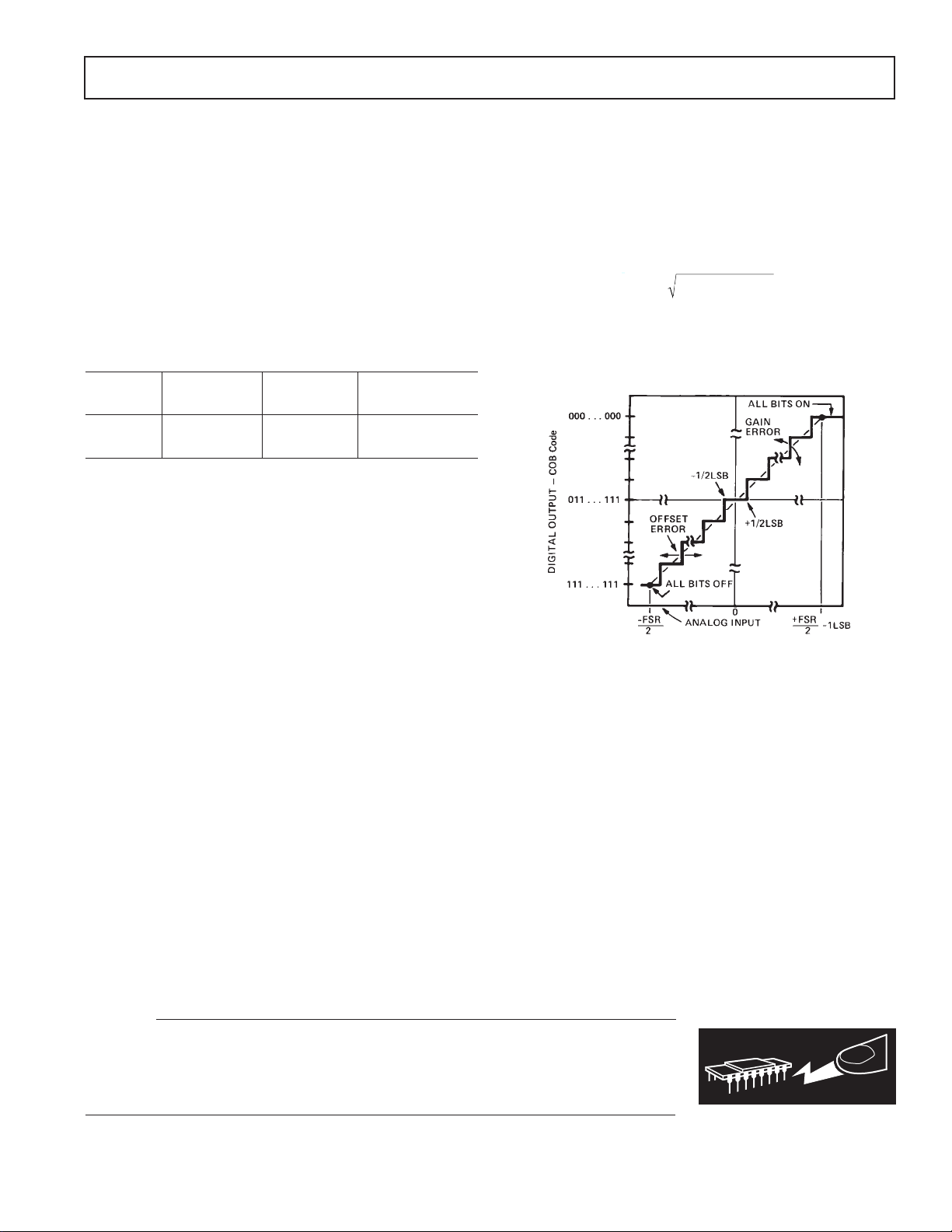
significant bit step size (Figure 1).
Monotonic behavior requires that the differential linearity error
be less than 1 LSB; however, a monotonic converter can have
missing codes. The AD1380 is specified as having no missing
codes over temperature ranges as specified on the data page.
There are three types of drift error over temperature: offset, gain
and linearity. Offset drift causes a shift of the transfer characteristic left or right on the diagram over the operating temperature
range. Gain drift causes a rotation of the transfer characteristic
about the zero for unipolar ranges or minus full-scale point for
bipolar ranges. The worst case accuracy drift is the summation
of all three drift errors over temperature. Statistically, however,
the drift error behaves as the root-sum-squared (RSS) and can
be shown as:
2
2
RSS =∈
G
+∈
2
+∈
O
L
∈G = Gain Drift Error (ppm/°C)
= 0ffset Drift Error (ppm of FSR/°C)
∈
O
= Linearity Error (ppm of FSR/°C)
∈
L
Figure 1. Transfer Characteristics for an Ideal Bipolar A/D
DESCRIPTION OF OPERATION
On receipt of a CONVERT START command, the AD1380
converts the voltage at its analog input into an equivalent 16-bit
binary number. This conversion is accomplished as follows: the
16-bit successive approximation register (SAR) has its 16-bit
outputs connected to both the device bit output pins and the
corresponding bit inputs of the feedback DAC. The analog
input is successively compared to the feedback DAC output,
one bit at a time (MSB first, LSB last). The decision to keep
or reject each bit is then made at the completion of each bit
comparison period, depending on the state of the comparator
at that time.
CAUTION
ESD (electrostatic discharge) sensitive device. Electrostatic charges as high as 4000 V readily
accumulate on the human body and test equipment and can discharge without detection.
Although the AD1380 features proprietary ESD protection circuitry, permanent damage may
occur on devices subjected to high energy electrostatic discharges. Therefore, proper ESD
precautions are recommended to avoid performance degradation or loss of functionality.
REV. B
–3–
WARNING!
ESD SENSITIVE DEVICE
 Loading...