

Page 1

January 2011
HIV51001-2.3
HIV51001-2.3
1. HardCopy IV Device Family Overview
This chapter provides an overview of features available in the HardCopy®IV device
family. More details about these features can be found in their respective chapters.
HardCopy IV ASICs are the only 40-nm system-capable ASICs designed with an
FPGA design flow. Altera's fifth generation of HardCopy IV ASICs deliver low-cost
and high-performance at low-power. Based on a 0.9-V, 40-nm process, the
HardCopy IV family is supported by Stratix®IV FPGAs, which have complementary
pin-outs, densities, and architectures that deliver in-system, at-speed prototyping—
resulting in first-time-right ASICs. The Quartus®II software provides a complete set
of tools for designing the Stratix IV FPGA prototypes and HardCopy IV ASICs. One
design, one RTL, one set of intellectual property, and one tool deliver both ASIC and
FPGA implementations. Other front-end design tools from Synopsys and Mentor
Graphics® are also supported.
To reduce risk, HardCopy IV device features, such as phase-locked loops (PLLs),
embedded memory, transceivers, and I/O elements (IOEs), are functionally and
electrically equivalent to the Stratix IV FPGA features. To reduce cost, Altera®
HardCopy IV devices are customized using only two metal and three via layers. The
combination of the Quartus II software for design, Stratix IV FPGAs for in-system
prototype and design verification, and HardCopy IV devices for high-volume
production provides the fastest time to market, lowest total cost, and lowest risk
system design and production solution to meet your business needs.
The HardCopy IV device family contains two variants optimized to meet different
application needs:
■ HardCopy IV GX transceiver ASICs—up to 11.5 M usable ASIC equivalent gates,
20,736 Kbits dedicated RAM, 1,288 18 × 18-bit multipliers, and 36 full-duplex clock
data recovery (CDR)-based transceivers at up to 6.5 Gbps
■ HardCopy IV E ASICs—up to 14.6 M usable ASIC equivalent gates, 18,792 Kbits
dedicated RAM, and 1,288 18 × 18 bit multipliers
© 2011 Altera Corporation. All rights reserved. ALTERA, ARRIA, CYCLONE, HARDCOPY, MAX, MEGACORE, NIOS, QUARTUS and STRATIX are Reg. U.S. Pat. & Tm. Off.
and/or trademarks of Altera Corporation in the U.S. and other countries. All other trademarks and service marks are the property of their respective holders as described at
www.altera.com/common/legal.html. Altera warrants performance of its semiconductor products to current specifications in accordance with Altera’s standard warranty, but
reserves the right to make changes to any products and services at any time without notice. Altera assumes no responsibility or li ab ility aris ing out of the app lic atio n or us e of any
information, product, or service described herein except as expressly agreed to in writing by Altera. Altera customers are advised to obtain the latest version of device
specifications before relying on any published information and before placing orders for products or services.
HardCopy IV Device Handbook Volume 1: Device Interfaces and Integration
January 2011
Subscribe
Page 2

1–2 Chapter 1: HardCopy IV Device Family Overview
Features
Features
HardCopy IV devices offer the following features:
■ General
■ Fine-grained HCell architecture resulting in a low-cost, high-performance,
low-power ASIC
■ Fully tested production-quality samples typically available 14 weeks from the
date of your design submission
■ Design functionality the same as the Stratix IV FPGA prototype
■ System performance and power
■ Core logic performance up to 50% faster than the Stratix IV FPGA prototype
■ Power consumption reduction of typically 50% from the Stratix IV FPGA
prototype
■ Robust on-chip hot socketing and power sequencing support
■ Support for instant-on or instant-on-after-50 ms power-up modes
■ I/O:GND:PWR ratio of 8:1:1 along with on-die and on-package decoupling for
robust signal integrity
1 The actual performance and power consumption improvements described
in this data sheet are design-dependent.
■ Transceivers (HardCopy IV GX family)
■ Up to 36 full-duplex CDR-based transceivers in HardCopy IV GX devices
supporting data rates up to 6.5 Gbps
■ Dedicated circuitry to support physical layer functionality for popular serial
protocols, such as PCI Express (PIPE) Gen1 and Gen2, Gigabit Ethernet, Serial
RapidIO, SONET/SDH, XAUI/HiGig, (OIF) CEI-6G, SD/HD/3G-SDI, Fibre
Channel, SFI-5, and Interlaken
■ Complete PCI Express (PIPE) protocol solution with embedded PCI Express
hard IP blocks that implement PHY-MAC layer, Data Link layer, and
Transaction layer functionality
■ Programmable transmitter pre-emphasis and receiver equalization circuitry to
compensate for frequency-dependent losses in the physical medium
■ Typical physical medium attachment (PMA) power consumption of 100 mW at
3.125 Gbps and 135 mW at 6.375 Gbps per channel
■ Logic and Digital Signal Processing (DSP)
■ 3.8 to 15 million usable gates for both logic and DSP functions (as shown in
Table 1–1)
■ High-speed DSP functions supporting 9 × 9, 12 × 12, 18 × 18, and 36 × 36
multipliers, multiple accumulate functions, and finite impulse response (FIR)
filters
HardCopy IV Device Handbook Volume 1: Device Interfaces and Integration January 2011 Altera Corporation
Page 3

Chapter 1: HardCopy IV Device Family Overview 1–3
Features
■ Internal memory
■ TriMatrix memory, consisting of three RAM block sizes to implement true
dual-port memory and first-in first-out (FIFO) buffers
■ Up to 20, 736 Kbits RAM in embedded RAM blocks (including parity bits)
■ Memory logic array blocks (MLAB) implemented in HCell logic fabric
■ Clock resources PLLs
■ Up to 16 global clocks, 88 regional clocks, and 88 peripheral clocks per device
■ Clock control block supporting dynamic clock network enable/disable and
dynamic global clock network source selection
■ Up to 12 PLLs per device supporting PLL reconfiguration, clock switchover,
programmable bandwidth, clock synthesis, and dynamic phase shifting
■ I/O standards, external memory interface, and intellectual property (IP)
■ Support for numerous single-ended and differential I/O standards, such as
LVTTL, LVCMOS, PCI, PCI-X, SSTL, HSTL, and LVDS
■ High-speed differential I/O support with serializer/deserializer (SERDES) and
dynamic phase alignment (DPA) circuitry for 1.25 Gbps performance
■ Support for high-speed networking and communications bus standards,
including SPI-4.2, SFI-4, SGMII, Utopia IV, 10 Gigabit Ethernet XSLI,
Rapid I/O, and NPSI
■ Memory interface support with dedicated DQS logic on all I/O banks
■ Dynamic On-Chip Termination (OCT) with auto-calibration support on all I/O
banks
■ Support for high-speed external memory interfaces, including DDR, DDR2,
DDR3 SDRAM, RLDRAM II, QDR II, and QDR II+ SRAM on up to 20 modular
I/O banks
■ Support for multiple intellectual property megafunctions from Altera
MegaCore® functions and Altera Megafunction Partners Program (AMPPSM)
■ Nios
■ JTAG—IEEE 1149.1 boundary scan testing (BST) support
■ Packaging
■ Pin-compatible with Stratix IV FPGA prototypes
■ Up to 880 user I/O pins available
■ Flip chip, space-saving FineLine BGA packages available (Table 1–5)
®
II embedded processor support
January 2011 Altera Corporation HardCopy IV Device Handbook Volume 1: Device Interfaces and Integration
Page 4
1–4 Chapter 1: HardCopy IV Device Family Overview
Features
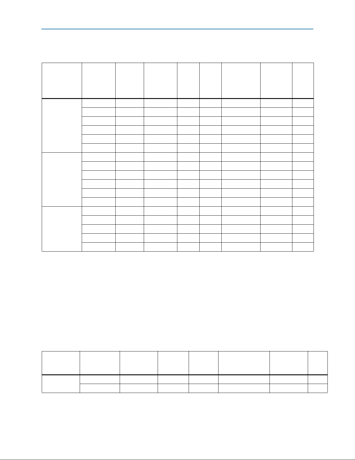
Table 1–1 and Table 1–2 list the HardCopy IV ASIC devices and available features.
Table 1–1. HardCopy IV GX ASIC Features
Tot al
Hard Copy IV G X
ASIC
Stratix IV GX
FPGA
Prototy pe
ASIC
Equivalent
Gates (1)
Transceivers
6.5 Gbps (2)
M9K
Blocks
M144K
Blocks
Dedicated
RAM Bits
(not including
18 × 18-Bit
Multi pliers
(FIR Mode)
PLLs
MLABs) (3)
EP4SGX70 2.8 M 8, 0 462 16 6,462 Kb 384 3
EP4SGX110 3.8 M 8, 0 660 16 8,244 Kb 512 3
EP4SGX180 6.7 M 8, 0 660 20 8,820 Kb 920 3
HC4GX15
EP4SGX230 9.2 M 8, 0 660 22 9,108 Kb 1,288 3
EP4SGX290 7.7 M 8, 0 660 24 9,396 Kb 832 2
EP4SGX360 9.4 M 8, 0 660 24 9,396 Kb 1,040 2
EP4SGX110 3.8 M 16, 0 660 16 8,244 Kb 512 4
EP4SGX180 6.7 M 16, 8 (6) 936 20 11,304 Kb 920 6
EP4SGX230 9.2 M 16, 8 (6) 936 22 11,592 Kb 1,288 6
HC4GX25
EP4SGX290 7.7 M 16, 8 (6) 936 36 13,608 Kb 832 6 (4)
EP4SGX360 9.4 M 16, 8 (6) 936 36 13,608 Kb 1,040 6 (4)
EP4SGX530 11.5 M 16, 8 (6) 936 36 13,608 Kb 1,024 6
EP4SGX180 6.7 M 24, 12 (7) 950 20 11,430 Kb 920 8
EP4SGX230 9.2 M 24, 12 (7) 1,235 22 14,283 Kb 1,288 8 (5)
EP4SGX290 7.7 M 24, 12 (7) 936 36 13,608 Kb 832 8
HC4GX35
EP4SGX360 9.4 M 24, 12 (7) 1,248 48 18,144 Kb 1,040 8 (5)
EP4SGX530 11.5 M 24, 12 (7) 1,280 64 20,736 Kb 1,024 8 (5)
Notes to Tab le 1– 1:
(1) This is the number of ASIC- equivalent gates ava ilable in the HardCopy IV base array, shared between both adaptive logic module (ALM) logic and
DSP functions from a Stratix IV FPGA prototype. The number of usable ASIC-equivalent gates is bounded by the number of ALMs in the
companion Stratix IV FPGA device.
(2) The first number indicates the number of transceivers with PMA and PCS; the second number indicates the number of CMU (PMA Only)
transceivers.
(3) MLAB RAMs are implemented with HCells in the HardCopy IV ASICs.
(4) This device has six PLLs in the F1152 package and four PLLs in the F780 package.
(5) This device has eight PLLs in the F1517 package and six PLLs in the F1152 package.
(6) Devices in the cost-optimized LF780 and LF1152 packages have 16 transceivers and no CMU transceiver. Devices in the performance-optimized
FF1152 package have 16 transceivers and eight CMU transceivers.
(7) Devices in the F1152 package have 16 transceivers a nd eight CMU t ransceivers. Devices in the performance-optimized F F1517 package have 24
transceivers and 12 CMU transceivers.
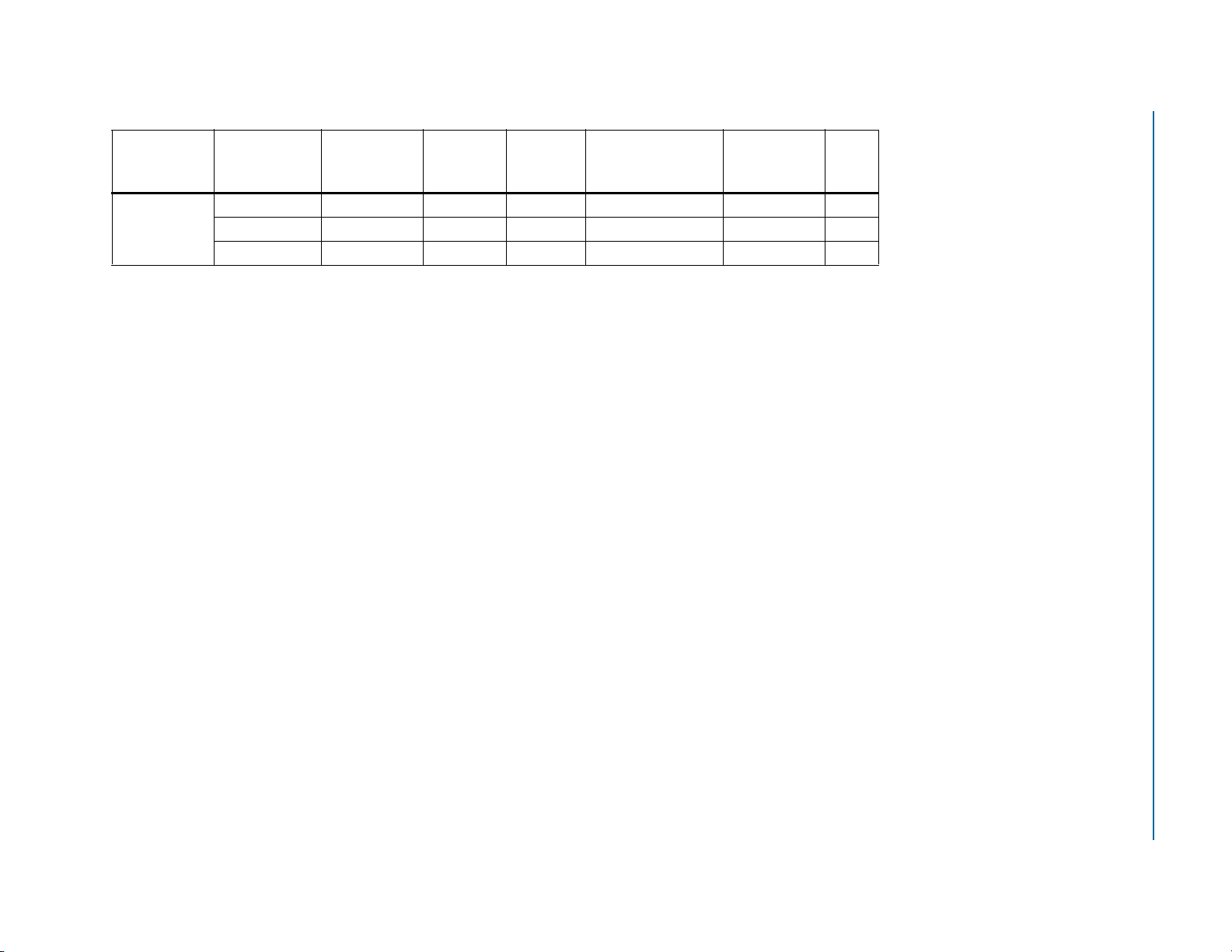
Table 1–2. HardCopy IV E ASIC Features (Part 1 of 2)
HardCopy IV E
ASIC
HC4E25
Stratix IV E
Prot otype
Device
EP4SE230 9.2 M 864 22 10,944 Kb 1,288 4
EP4SE360 9.4 M 864 32 12,384 Kb 1,040 4
ASIC
Equivalent
Gates (1)
M9K
Blocks
M144K
Blocks
Total Dedicated
RAM Bits (excluding
MLABs) (2)
18 × 18-Bit
Multipliers
(FIR Mode)
PLLs
HardCopy IV Device Handbook Volume 1: Device Interfaces and Integration January 2011 Altera Corporation
Page 5
Chapter 1: HardCopy IV Device Family Overview 1–5
January 2011 Altera Corporation HardCopy IV Device Handbook Volume 1: Device Interfaces and Integration
Table 1–2. HardCopy IV E ASIC Features (Part 2 of 2)
Features
HardCopy IV E
ASIC
HC4E35
Notes to Ta bl e 1– 2:
(1) This is the number of ASIC-equivalent gates available in the HardCopy IV E base array, shared between both adaptive logic module (ALM) logic and DSP functions
from a Stratix IV E FPGA prototype. The number of usable ASIC-equivalent gates is bounded by the number of ALMs in the companion Stratix IV E FPGA device.
(2) MLAB RAMs are implemented with HCells in the HardCopy IV ASICs.
(3) This device has 12 PLLs in the F1517 package and eight PLLs in the F1152 package.
Stratix IV E
Prototype
Device
EP4SE360 9.4 M 1,248 48 18,144 Kb 1,040 8
EP4SE530 11.5 M 1,280 48 18,432 Kb 1,024 12 (3)
EP4SE820 14.6 M 1,320 48 18,792 Kb 960 12 (3)
ASIC
Equivalent
Gates (1)
M9K
Blocks
M144K
Blocks
Total Dedicated
RAM Bits (excludin g
MLABs) (2)
18 × 18-Bit
Multipliers
(FIR Mode)
PLLs
HardCopy IV ASIC and Stratix IV FPGA Mapping Paths
HardCopy IV devices offer pin-to-pin compatibility with the Stratix IV prototype, making them drop-in replacements for the
FPGAs. Therefore, the same system board and software developed for prototyping and field trials can be retained, enabling the
lowest risk and fastest time-to-market for high-volume production.
HardCopy IV devices also offer non-socket replacement mapping paths to smaller standard or customized packages. For
example, you can map the EP4SE230 device in the 780-pin FBGA package to the HC4E25 device in the 484-pin FBGA standard
package, or to the 400-pin FBGA customized package. Because the pin-out for the two packages are not the same, you need a
separate board design for the Stratix IV device and the HardCopy IV device.
The non-socket replacement offerings extend cost reduction further and allow for a smaller foot print occupied by the
HardCopy IV device. The non-socket replacement to a standard package is supported in the Quartus II software. The
customized package option is not visible in the Quartus II software. For more information, refer to “HardCopy IV Package
Pro” on page 1–9.
For the non-socket replacement to a standard package, select I/Os in the Stratix IV device that can be mapped to the
HardCopy IV device. Not all I/Os in the Stratix IV device are available in the HardCopy IV non-socket replacement device.
Check the pin-out information for both the Stratix IV device and HardCopy IV device to ensure that the I/Os can be mapped,
and select the companion device in the Quartus II project setting during design development. By selecting the companion
device, the Quartus II software ensures that common resources and compatible I/Os are used during the mapping from the
Stratix FPGA to the HardCopy ASIC.
There are a number of FPGA prototype choices for each HardCopy IV device, as listed in Table 1–3 and Table 1–4. To obtain the
best value and the lowest system cost, architect your system to maximize silicon resource utilization.
Page 6
HardCopy IV Device Handbook Volume 1: Device Interfaces and Integration January 2011 Altera Corporation
1–6 Chapter 1: HardCopy IV Device Family Overview
Table 1–3. Stratix IV GX FPGA Prototy pe-to-HardCopy IV GX ASIC Mapping Paths
HardCopy IV GX ASIC
Device Package
HC4GX15
780-pin
FineLine BGA
780-pin
HC4GX25
FineLine BGA
1152-pin
FineLine BGA
1152-pin
HC4GX35
FineLine BGA
1517-pin
FineLine BGA
Note to Tab le 1 –3 :
(1) The Hybrid FBGA package for Stratix IV GX FPGAs requires additional unused board space along the edges beyond the footprint, but its foot print is compatible with the regular FBGA package. HardCopy IV GX
ASICs are in the regular FBGA packages.
EP4SGX70 EP4SGX110 EP4SGX180 EP4SGX230 EP4SGX290 EP4SGX360 EP4SGX530
F780 F780 F1152 F780 F1152 F1517 F780 F1152 F1517 H780 F1152 F1517 H780 F1152 F1517 H1152 H1517
vv — v — — v ——
— ————————
—— v — v —— v —— v ——v —
— ——————v —————
— ————v ——v ——v —
Stratix IV GX FPGA Prototype and Package
v
(1)
v
(1)
——
——
v
(1)
v
(1)
——— —
——— —
v
—
—
v
v
(1)
v
(1)
—
—
—
v
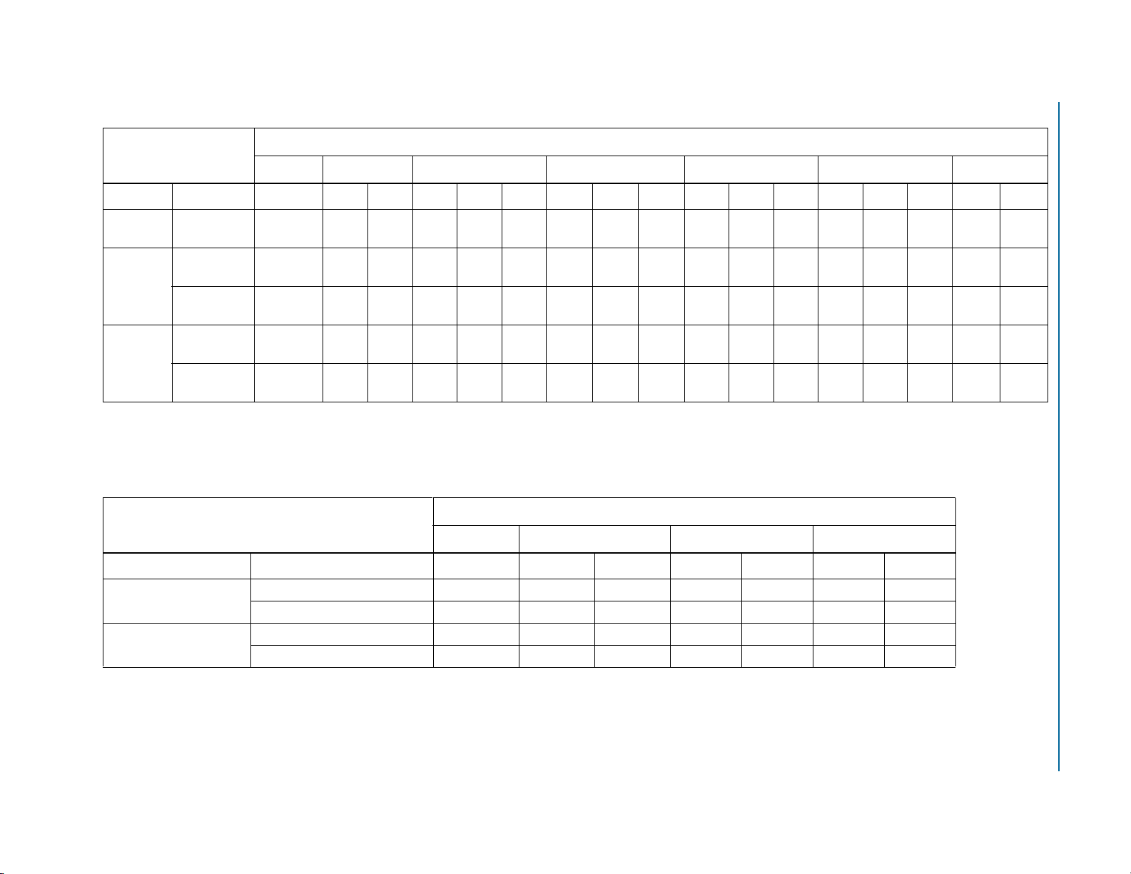
Table 1– 4. Stratix IV E FPGA Prototy pe-to-HardCopy IV E ASIC Mapping Paths
HardCopy IV E ASIC
EP4SE230 EP4SE360 EP4SE530 EP4SE820
Stratix IV E FPGA Prototype and Package
Device Package
HC4E25
HC4E35
Notes to Table 1 –4:
(1) This mapping is a non-socket replacement path that requires a different board design for the Stratix IV E device and the HardCopy IV E device.
(2) The Hybrid FBGA package for the Stratix IV E FPGAs requires additional unused board space along the edges beyond the footprint, but its footprint is c ompatible with the regular FBGA
package. The HardCopy IV E ASICs are in the regular FBGA packages.
484-pin FineLine BGA v (1) — — ————
780-pin FineLine BGA vv (2) —————
1152-pin FineLine BGA — — vv (2) — v (2) —
1517-pin FineLine BGA — — — — v (2) — v
F780 H780 F1152 H1152 H1517 H1152 H1517
Features
Page 7

Chapter 1: HardCopy IV Device Family Overview 1–7
Features
Three different FineLine BGA package substrate options are available for the
HardCopy IV devices:
■ Performance-optimized flip chip package (F)
■ Cost-optimized flip chip package (L, LA)
■ Low-cost wire bond package (W)—available for HardCopy IV E ASICs only
All three package types support direct replacement of the Stratix IV FPGA prototype.
The performance-optimized flip chip package supports equivalent performance and
the same number of I/Os as the corresponding FPGA prototype. The cost-optimized
flip chip package uses a substrate with fewer layers and no on-package decoupling
(OPD) capacitors to offer a low-cost package option. The performance is reduced from
that of the FPGA prototype. However, the number of available I/Os remains the
same. The wire bond package offers another low-cost package option, but with the
trade-off of reduced performance and fewer available I/Os.
1 If you are going to use the low-cost wire bond package, make sure your design uses
I/Os that are available in that package.
For HardCopy IV E non-socket replacement devices, only the performance-optimized
flip chip package and the low-cost wire bond package are supported.
Table 1–5 and Table 1–6 show the available packages for HardCopy IV devices.
Table 1–5. HardCopy IV GX and Stratix IV GX Package, I/O Pin Count, LVDS Pair Count, and Transceiver Mapping
(Part 1 of 2) (Note 1), (2)
HardCopy IV
GX ASIC
HC4GX15
HC4GX25
HC4GX35
Companion
Mapping
LAF780 (3) LF780 (4) LF1152 (5) FF1152 (5) FF1517 (6)
372, 28, 8+0 257, 0, 8+0 — — — — —
— 289, 0, 16+0 564, 44, 16+0 564, 44, 16+8 — 564, 44, 16+8 —
— — — — 564, 44, 16+8 564, 44, 16+8 744, 88, 24+12
Stratix IV GX
FPGA
Prototype
EP4SGX70
EP4SGX110
EP4SGX180
EP4SGX230
EP4SGX290
EP4SGX360
F780 H780 F1152 F1152 F1152 H1152 F1517
372, 28, 8+0 — — — — — —
372, 28, 8+0 — 372, 28, 16+0 — — — —
372, 28, 8+0 — 564, 44, 16+0 564, 44, 16+8 — — 744, 88, 24+12
372, 28, 8+0 — 564, 44, 16+0 564, 44, 16+8 564, 44, 16+8 — 744, 88, 24+12
— 289, 0, 16+0 564, 44, 16+0 564, 44, 16+8 — — 744, 88, 24+12
— 289, 0, 16+0 564, 44, 16+0 564, 44, 16+8 564, 44, 16+8 — 744, 88, 24+12
January 2011 Altera Corporation HardCopy IV Device Handbook Volume 1: Device Interfaces and Integration
Page 8

1–8 Chapter 1: HardCopy IV Device Family Overview
Features
Table 1–5. HardCopy IV GX and Stratix IV GX Package, I/O Pin Count, LVDS Pair Count, and Transceiver Mapping
(Part 2 of 2) (Note 1), (2)
HardCopy IV
GX ASIC
EP4SGX530
Notes to Tab le 1– 5:
(1) The numbers in the table indicate I/O pin count, full duplex LVDS pairs, and transceivers (PMA and PCS) + CMU transceivers (PMA Only).
(2) The first letter (two letters in the LA packa ge) in the HardCopy IV GX package name refers to the following: F–Performance-optimized flip chip
package, L or LA –Cost-optimized flip chip package.
(3) The I/O pin count for the LAF780 package includes the four dedicated clock inputs (
(4) The I/O pin count for the LF780 package includes one dedicated clock input (
(5) The I/O pin count for the F1152 package includes the four dedicated clock inputs (
(6) The I/O pin count for the F1517 package includes the eight dedicated clock inputs (
CLK10p
LAF780 (3) LF780 (4) LF1152 (5) FF1152 (5) FF1517 (6)
— — — — — 564, 44, 16+8 744, 88, 24+12
CLK1n, CLK1p, CLK3n
CLK1p
).
CLK1n, CLK1p, CLK10n
).
CLK1n, CLK1p, CLK3n, CLK3p, CLK8n, CLK8p, CLK10n
, and
, and
CLK3p
CLK10p
).
).
, and
Table 1–6. HardCopy IV E and Stratix IV E Package, I/O Pin Count, and LVDS Pair Count Mapping (Note 1), (2), (3), (4)
HardCopy IV E
ASIC
HC4E25
HC4E35
WF484
FF484
WF780 FF780
LF1152
FF1152
LF1517
FF1517
296, 48 392, 48 488, 56 — —
— — — 744, 88 880, 88
Companion
Mapping
Strat ix IV E
FPGA
Prototype
EP4SE230
EP4SE360
EP4SE530
EP4SE820
Notes to Tab le 1– 6:
(1) The numbers in the table indicate I/O pin count, full duplex LVDS pairs.
(2) The first letter in the HardCopy IV E package name refers to the following: F–Performance-optimized flip chip package, L–Cost opt imized
flip-chip package, W–Low-cost wire bond package.
(3) For the F484, F780, and F1152 packaged device s, the I/O pin counts include the eight dedicated cloc k inputs (
CLK8n, CLK10p
(4) For the F1517 packaged device, the I/O pin count includes the eight dedicated clock inputs (
and
CLK10n
PLL_R4_CLKn, PLL_R1_C LKp
F780 F780 H780 F780 H780 F1152 H1152 F1517 H1517
488, 56 488, 56 — 488, 56 — — — — —
— — 488, 56 — 488, 56 744, 88 — — —
— —————744, 88 — 976, 112
— —————744, 88 — 976, 112
, and
CLK10n
) that you can use for inputs.
) and the eight dedicated corner PLL clock inputs (
, and
PLL_R1_CLK n
) that you can use for data inputs.
PLL_L1_CLK p, PLL_L1_CLKn, PLL_L4_CLKp, PLL_L4_CLK n, PLL_R4_CLKp
CLK1p, CLK1n, CLK3p, CLK3n, CLK8p, CLK8n, CLK10p
CLK1p, CLK1n, CLK3p, CLK3n, CLK8p
,
,
,
HardCopy IV Device Handbook Volume 1: Device Interfaces and Integration January 2011 Altera Corporation
Page 9

Chapter 1: HardCopy IV Device Family Overview 1–9
Features
HardCopy IV Package Pro
The Hardcopy IV Package Pro is a customized package program, which gives you the
option to select a package tailored to the number of I/O's used in your design. This
customized package will support less I/O's than what is available as a standard
package offering. HardCopy IV Package Pro will have a smaller foot print than a
Stratix IV FPGA prototype or a HardCopy IV non-socket replacement standard
package. The optimized package may further extend the cost savings over traditional
HardCopy IV device offerings.
The HardCopy IV Package Pro option is available for the HardCopy IV E device.
A HardCopy IV GX option is not offered at this time. Table 1–7 lists the available
FineLine Ball-Grid Array (FBGA) packages and the maximum supported I/O for
HardCopy IV E devices.
Table 1–7. HardCopy IV E FBGA Maximum I/O Pin Count
HardCopy IV E
ASIC
FF400 FF484 WF572 (1) FF572 WF672 (1) FF672 FF780 FF1020
Package
Dimension (mm)
21 × 21 23 × 23 25 × 25 25 × 25 27 × 27 27 × 27 29 × 29 33 × 33
(2)
HC4E25 216 — 336 336 384 384 — —
HC4E35 — 264 — 304 — 352 456 640
Notes to Tab le 1– 7:
(1) Low-Cost Wirebond Package (W)
(2) Dimensions are approximate. See the Altera Dev ice Package Information Datasheet for specifications that resemble the package offering in this
table.
HardCopy IV Package Pro is also offered in Ultra FineLine Ball-Grid Array (UBGA)
packages. These packages have a 0.8 mm ball pitch, which increases the I/O count
when compared to an FPGA package of the same dimension. Table 1–8 lists the
available UBGA packages and the maximum supported I/O for HardCopy IV E
devices.
Table 1–8. HardCopy IV E UBGA Maximum I/O Pin Count
HardCopy IV E ASIC FU572 FU672 WU780 (1) FU780
Package Dimension (mm)
(2)
21 × 21 23 × 23 25 × 25 25 × 25
HC4E25 336 384 384 480
HC4E35 — 352 — 456
Notes to Tab le 1– 8:
(1) Low-Cost Wirebond Package (W)
(2) Dimensions are approximate. See the Altera Device Package Information Datasheet for specifications that
resemble the package offering in this table.
HardCopy IV Package Pro is not visible in the Quartus II software, so you will not be
able to select a Package Pro device as a companion device to your Stratix IV device.
However, you still need the Quartus II software to compile your design into an
appropriate HardCopy IV device prior to migrating to a Package Pro option.
January 2011 Altera Corporation HardCopy IV Device Handbook Volume 1: Device Interfaces and Integration
Page 10

1–10 Chapter 1: HardCopy IV Device Family Overview
Features
1 HardCopy IV Package Pro details and specifications are not provided in the
HardCopy IV handbook, and electrical and thermal performance must be considered
when designing with Package Pro. Contact your Altera representative to engage the
HardCopy IV Package Pro program.
Differences Between HardCopy IV and Stratix IV Devices
HardCopy IV devices have several architectural differences from Stratix IV devices.
When implementing your design and laying out your board, consider these
differences. Use the following information to ensure that your design maps from the
Stratix IV FPGA to the HardCopy IV ASIC:
■ Configuration is not required for HardCopy IV devices; therefore, the following
Stratix IV features are not supported:
■ Programming modes and features such as remote update and Programmers
Object File (.pof) encryption
■ Cyclical redundancy check (CRC) for configuration error detection
■ 256-bit (AES) volatile and non-volatile security keys to protect designs
■ JTAG instructions used for configuration.
■ FPGA configuration emulation mode is not supported in HardCopy IV devices.
■ Boundary scan (BSCAN) chain length is different and varies with device density.
■ HardCopy IV devices contain up to a maximum of 20 I/O banks; Stratix IV
devices contain up to a maximum of 24 I/O.
■ Memory Initialization Files (.mif) for embedded memories used as RAM are not
supported. The .mifs for memories used as ROM are supported, because the data
are mask-programmed into the memory cells.
■ Stratix IV LAB, MLAB, and DSP functions are implemented with HCells in
HardCopy IV devices instead of dedicated blocks. However, they remain
functionally and electrically equivalent between the FPGAs and the HardCopy
ASICs.
■ Stratix IV programmable power technology is not supported in HardCopy IV
devices. However, the HardCopy IV architecture offers performance similar to
Stratix IV devices with significantly lower power consumption.
■ There are eight on-chip termination (OCT) calibration blocks in HardCopy IV
devices instead of up to 10 OCT calibration blocks in Stratix IV devices.
HardCopy IV Device Handbook Volume 1: Device Interfaces and Integration January 2011 Altera Corporation
Page 11

Chapter 1: HardCopy IV Device Family Overview 1–11
Architectural Features
Architectural Features
This section describes the architectural features of HardCopy IV ASICs.
Logic Array Block and Adaptive Logic Module Function Support
HardCopy IV devices fully support the Stratix IV LAB and ALM functions. The basic
building blocks of Stratix IV LABs are composed of ALMs that you can configure to
implement logic, arithmetic, and register functions. Each LAB consists of 10 ALMs,
carry chains, shared arithmetic chains, LAB control signals, local interconnect, and
register chain connection lines.
In HardCopy IV devices, the basic building blocks of the core array are HCells, which
are a collection of logic transistors connected together to provide the same
functionality as the Stratix IV LABs and ALMs. The Quartus II software maps these
LAB and ALM functions to HCell macros, which define how the HCells are connected
together in the HardCopy IV core array. Only HCells required to implement the
customer design are used, and unused HCells are powered down. This allows
efficient use of the core fabric and offers significant static power savings.
The Stratix IV LAB derivative, called MLAB, is also supported in HardCopy IV
devices. The MLAB adds static random access memory (SRAM) capability to the LAB
and can provide a maximum of 640 bits of simple dual-port SRAM. Like the LAB
functions, the Quartus II software maps MLAB functions to HCell macros in
HardCopy IV devices to provide the same Stratix IV functionality.
f For more information about LABs and ALMs, refer to the Logic Array Block and
Adaptive Logic Module Implementation in HardCopy IV Devices chapter.
f For more information about MLAB modes, features, and design considerations, refer
to the TriMatrix Embedded Memory Blocks in HardCopy IV Devices chapter.
DSP Function Support
HardCopy IV devices fully support the DSP block functions of Stratix IV devices.
Complex systems such as WiMAX, 3GPP WCDMA, CDMA2000, voice over Internet
protocol (VoIP), H.264 video compression, and high-definition television (HDTV)
require high-performance DSP circuits to handle large amounts of data with high
throughput. These system designs typically use DSP to implement finite impulse
response (FIR) filters, complex FIR filters, infinite impulse response (IIR) filters, fast
Fourier transform (FFT) functions, and discrete cosine transform (DCT) functions.
In HardCopy IV devices, these DSP block functions are implemented with HCells.
The Quartus II software maps the Stratix IV DSP functions to HCell macros in
HardCopy IV devices, preserving the same functionality. Implementing DSP
functions using HCells also allows efficient use of the HardCopy IV device core fabric
and offers significant static power savings.
HardCopy IV devices support all Stratix IV DSP configurations (9 × 9, 12 × 12, 18 × 18,
and 36 × 36 multipliers) and block features, such as dynamic sign controls, dynamic
addition and subtraction, dynamic rounding and saturation, and dynamic input shift
registers. All five operational modes of the Stratix IV DSP block are supported:
■ Independent multiplier (9 × 9, 12 × 12, 18 × 18, and 36 × 36)
January 2011 Altera Corporation HardCopy IV Device Handbook Volume 1: Device Interfaces and Integration
Page 12

1–12 Chapter 1: HardCopy IV Device Family Overview
Architectural Features
■ Two-multiplier adder
■ Four-multiplier adder
■ Multiply accumulate
■ Shift mode
f For more information about DSP blocks, refer to the DSP Block Implementation in
HardCopy IV Devices chapter.
TriMatrix Embedded Memory Blocks
TriMatrix embedded memory blocks provide three different sizes of embedded
SRAM to efficiently address the needs of HardCopy IV ASIC designs. TriMatrix
memory includes the following types of blocks:
■ 640-bit MLAB blocks optimized to implement filter delay lines, small FIFO buffers,
and shift registers. MLAB blocks are implemented in HCell macros.
■ 9-Kbit M9K blocks that can be used for general purpose memory applications.
■ 144-Kbit M144K blocks that are ideal for processor code storage, packet, and video
frame buffering.
You can configure each embedded memory block independently to be a single- or
dual-port RAM, ROM, or shift register using the Quartus II MegaWizard™ Plug-In
Manager. Multiple blocks of the same type can also be stitched together to produce
larger memories with minimal timing penalty. TriMatrix memory provides up to an
equivalent of 20.3 Mbits of dedicated, embedded SRAM.
f For more information about TriMatrix memory blocks, modes, features, and design
considerations, refer to the TriMatrix Embedded Memory Blocks in HardCopy IV Devices
chapter.
Clock Networks and PLLs
HardCopy IV devices provide dedicated global clock networks (GCLKs), regional
clock networks (RCLKs), and periphery clock networks (PCLKs). These clocks are
organized into a hierarchical clock structure that provides up to 192 unique clock
domains (16 GCLK + 88 RCLK + 88 PCLK) within the HardCopy IV device and allows
up to 60 unique GCLK/RCLK/PCLK clock sources (16 GCLK + 22 RCLK + 22 PCLK)
per device quadrant.
HardCopy IV devices deliver abundant PLL resources, with up to 12 PLLs per device
and up to 10 outputs per PLL. You can configure each output independently, creating
a unique, customizable clock frequency with no fixed relation to any other input or
output clock. Inherent jitter filtration and fine granularity control over multiply,
divide ratios, and dynamic phase-shift reconfiguration provide the high-performance
precision required in today’s high-speed applications. HardCopy IV PLLs are
feature-rich, supporting advanced capabilities such as clock switchover,
reconfigurable phase shift, PLL reconfiguration, and reconfigurable bandwidth. You
can use PLLs for general-purpose clock management, supporting multiplication,
phase shifting, and programmable duty cycles. HardCopy IV PLLs also support
external feedback mode, spread-spectrum input clock tracking, and post-scale counter
cascading.
HardCopy IV Device Handbook Volume 1: Device Interfaces and Integration January 2011 Altera Corporation
Page 13

Chapter 1: HardCopy IV Device Family Overview 1–13
Architectural Features
f For more information about clock networks and PLLs, refer to the Clock Networks and
PLLs in HardCopy IV Devices chapter.
I/O Banks and I/O Structure
HardCopy IV devices contain up to 20 modular I/O banks, each containing 24, 32, 40,
or 48 I/Os (not including dedicated clock inputs). The left- and right-side I/O banks
contain circuitry to support external memory interfaces and high-speed differential
I/O interfaces capable of performance at up to 1.25 Gbps. The top and bottom I/O
banks also contain circuitry to support external memory interfaces.
HardCopy IV devices support a wide range of industry I/O standards, including
single-ended, voltage referenced single-ended, and differential I/O standards. The
HardCopy IV I/O supports bus hold, pull-up resistor, slew rate, output delay control,
and open-drain output. HardCopy IV devices also support on-chip series (RS) and
on-chip parallel (RT) termination with auto calibration for single-ended I/O
standards. The left and right I/O banks support on-chip differential termination (RD)
to meet LVDS I/O standards. Bidirectional I/O pins on all I/O banks also support
Dynamic OCT.
f For more information about I/O features, refer to the HardCopy IV Device I/O Features
chapter.
External Memory Interfaces
The HardCopy IV I/O structure is equivalent to the Stratix IV I/O structure,
providing high-performance support for existing and emerging external memory
standards such as DDR, DDR2, DDR3, QDRII, QDRII+, and RLDRAM II.
Packed with features such as dynamic on-chip termination, trace mismatch
compensation, read and write leveling, half-rate registers, and 4- to 36-bit DQ group
widths, HardCopy IV I/Os supply the built-in functionality required for rapid and
robust implementation of external memory interfaces. Double data-rate support is
found on all sides of the HardCopy IV device. HardCopy IV devices provide an
efficient architecture to quickly and easily fit wide external memory interfaces
precisely.
A self-calibrating soft IP core (ALTMEMPHY) optimized to take advantage of
HardCopy IV device I/Os along with the Quartus II timing analysis tool (the
TimeQuest Timing Analyzer) provides the total solution for the highest reliable
frequency of operation across process, voltage, and temperature (PVT).
f For more information about external memory interfaces, refer to the External Memory
Interfaces in HardCopy IV Devices chapter.
High-Speed Differential I/O Interfaces with DPA
HardCopy IV devices contain dedicated circuitry for supporting differential
standards at speeds up to 1.25 Gbps. High-speed differential I/O circuitry supports
the following high-speed I/O interconnect standards and applications:
■ Utopia IV
■ SPI-4.2
January 2011 Altera Corporation HardCopy IV Device Handbook Volume 1: Device Interfaces and Integration
Page 14

1–14 Chapter 1: HardCopy IV Device Family Overview
Architectural Features
■ SFI-4
■ 10 Gigabit Ethernet XSLI
■ Rapid I/O
■ NPSI
HardCopy IV devices support 2×, 4×, 6×, 7×, 8×, and 10× SERDES modes for
high-speed differential I/O interfaces, and 4×, 6×, 7×, 8×, and 10× SERDES modes
when using the dedicated DPA circuitry. DPA minimizes bit errors, simplifies PCB
layout and timing management for high-speed data transfer, and eliminates
channel-to-channel and channel-to-clock skews in high-speed data transmission
systems. The Stratix IV soft CDR function can also be implemented using HCells in
HardCopy IV devices, enabling low-cost 1.25-Gbps clock-embedded serial links.
HardCopy IV devices have the following dedicated circuitry for high-speed
differential I/O support:
■ Differential I/O buffer
■ Transmitter serializer
■ Receiver deserializer
■ Data realignment
■ Dynamic phase aligner (DPA)
■ Soft CDR functionality
■ Synchronizer (FIFO buffer)
■ PLLs
f For more information about dedicated circuitry for high-speed differential support,
refer to the High Speed Differential I/O Interfaces with DPA in HardCopy IV Devices
chapter.
Hot Socketing and Power-On Reset
HardCopy IV devices offer hot socketing, which is also known as hot plug-in or hot
swap, and power sequencing support without the use of any external devices.
On-chip hot socketing and power-sequencing support ensures proper device
operation independent of the power-up sequence. You can insert or remove a
HardCopy IV board during system operation without causing undesirable effects to
the running system bus or the board itself.
The hot socketing feature also makes it easier to use HardCopy IV devices on PCBs
that contain a mixture of 3.0-V, 2.5-V, 1.8-V, 1.5-V, and 1.2-V devices. With the
HardCopy IV hot socketing feature, you do not need to ensure a proper power-up
sequence for each device on the board.
1 HardCopy IV devices have a maximum V
voltage of 3.0 V, but can tolerate a 3.3-V
CCIO
input level.
f For more information about hot socketing, refer to the Hot Socketing and Power-On
Reset in HardCopy IV Devices chapter.
HardCopy IV Device Handbook Volume 1: Device Interfaces and Integration January 2011 Altera Corporation
Page 15

Chapter 1: HardCopy IV Device Family Overview 1–15
Software Support and Part Number Information
IEEE 1149.1 (JTAG) Boundary Scan Testing
HardCopy IV devices support the JTAG IEEE Std. 1149.1 specification. The
Boundary-Scan Test (BST) architecture offers the capability to both test pin
connections without using physical test probes and capture functional data while a
device is operating normally. Boundary-scan cells in the HardCopy IV device can
force signals onto pins or capture data from the pin or core signals. Forced test data is
serially shifted into the boundary-scan cells. Captured data is serially shifted out and
externally compared to expected results.
f For more information about JTAG, refer to the IEEE 1149.1 (JTAG) Boundary Scan
Testing in HardCopy IV Devices chapter.
Signal Integrity
HardCopy IV devices simplify the challenge of maintaining signal integrity through a
number of chip-, package-, and board-level enhancements to enable efficient
high-speed data transfer into and out of the device. These enhancements include:
■ 8:1:1 user I/O/GND/V
■ Dedicated power supply for each I/O bank, with an I/O limit of 24 to 48 I/Os per
ratio to reduce loop inductance in the package
CC
bank to help limit simultaneous switching noise (SSN)
■ Slew-rate support with up to four settings to match the desired I/O standard,
control noise, and overshoot
■ Output-current drive strength support with up to four settings to match desired
I/O standard performance
■ Output-delay support to control rise and fall times and adjust duty cycle,
compensate for skew, and reduce simultaneous switching output (SSO) noise
■ Dynamic OCT with auto-calibration support for series and parallel OCT and
differential OCT support for LVDS I/O standard on the left and right banks
1 The supported settings for slew-rate control, output-current drive strength, and
output-delay control are mask-programmed into the HardCopy IV devices and
cannot be changed after the silicon is fabricated.
f For more information about signal integrity support in the Quartus II software, refer
to the Quartus II Handbook.
Software Support and Part Number Information
This section describes HardCopy IV device software support and part number
information.
January 2011 Altera Corporation HardCopy IV Device Handbook Volume 1: Device Interfaces and Integration
Page 16

1–16 Chapter 1: HardCopy IV Device Family Overview
Software Support and Part Number Information
Software Support
HardCopy IV devices are supported by the Altera Quartus II design software, which
provides a comprehensive environment for system-on-chip (SOC) design. The
Quartus II software includes HDL and schematic design entry, compilation and logic
synthesis, full simulation and advanced timing analysis, SignalTap™II logic analyzer,
and device configuration.
f For more information about the Quartus II software features, refer to the Quartus II
Handbook.
The Quartus II software supports the Windows and Linux Red Hat operating
systems. You can obtain the specific operating system for the Quartus II software from
the Quartus II Readme.txt file or
http://www.altera.com/download/os-support/oss-index.html. The Quartus II
software also supports seamless integration with industry-leading EDA tools through
the NativeLink interface.
Part Number Information
Figure 1–1 shows the generic part number for HardCopy IV devices.
Figur e 1–1. HardCopy IV Device Part Number Information
HC4GX 35
HC4GX: HardCopy IV GX Family
HC4E: HardCopy IV E Family
Device Type
15 (HardCopy IV GX only)
25
35
Package Subsrate
Typ e
F: Performance-optimized flip chip package
L, LA: Cost-Optimized flip chip package
W: Low-cost wire bond package
F
Package Type
F: FineLine BGA (FBGA)
F
1517
N
Optional SuffixFa m i l y S i g n a t u r e
Indicat es specific device options
N: RoHS compliant
Pin Count
Number of pins for a particular package:
484
780
1152
1517
HardCopy IV Device Handbook Volume 1: Device Interfaces and Integration January 2011 Altera Corporation
Page 17

Chapter 1: HardCopy IV Device Family Overview 1–17
Document Revision History
Document Revision History
Table 1–9 lists the revision history for this chapter.
Table 1–9. Document Revision History
Date Version Changes
■ Updated “Features” on page 1–2.
■ Updated “HardCopy IV ASIC and Stratix IV FPGA Mapping Paths” on page 1–5.
January 2011 2.3
January 2010 2.2
July 2009 2.1 Updated “Features” on page 1–2
June 2009 2.0
December 2008 1.0 Initial release.
■ Added “HardCopy IV Package Pro” on page 1–9.
■ Used new document template.
■ Made minor text edits.
■ Updated Table 1–2.
■ Updated Table 1–5.
■ Updated Table 1–8.
■ Made minor text edits.
■ Updated “Introduction” on page 1–1.
■ Updated “Features” on page 1–2.
■ Updated Table 1–1.
■ Added Table 1–2
■ Updated Table 1–3.
■ Added Table 1–4
■ Added Table 1–5.
■ Added Table 1–6
■ Updated Figure 1–1.
January 2011 Altera Corporation HardCopy IV Device Handbook Volume 1: Device Interfaces and Integration
Page 18

1–18 Chapter 1: HardCopy IV Device Family Overview
Document Revision History
HardCopy IV Device Handbook Volume 1: Device Interfaces and Integration January 2011 Altera Corporation
 Loading...