

Page 1
2015.03.06
www.altera.com
101 Innovation Drive, San Jose, CA 95134
Device-Specific Power Delivery Network (PDN) Tool
2.0 User Guide
UG-01157
Subscribe
Send Feedback
This user guide provides a brief overview of the various tabs in the device-specific PDN tool 2.0. You can
quickly and accurately design a robust power delivery network with the PDN tool 2.0. This is done by
calculating an optimum number of capacitors that meet the target impedance requirements for a given
power supply.
Note: The PDN tool 2.0 only supports Microsoft Excel 2007 and newer, and either US or UK English
language.
Table 1: PDN Tool 2.0 Software Verification
Altera® has tested and verified that the PDN tool 2.0 is compatible with these platforms and software versions.
Operating System Excel Versions
Windows 8 (32-bit) 2007, 2010, 2013
Windows 8 (64-bit) 2010, 2013
Windows 7 (32-bit) 2007, 2010, 2013
Windows 7 (64-bit) 2010, 2013
Windows XP 2007, 2010
Overview
The Altera PDN tool 2.0 helps PCB designers estimate the number, value, and type of decoupling
capacitors needed to develop an efficient PCB decoupling strategy. It allows you to do this during the
early design phase, without going through extensive pre-layout simulations.
The PDN tool 2.0 is a Microsoft Excel-based spreadsheet that calculates an impedance profile based on
your input. For a given power supply, the spreadsheet only requires basic design information to calculate
the impedance profile and the optimum number of capacitors to meet the desired impedance target
(Z
TARGET
specifications, for example. The tool also provides device- and power rail-specific PCB decoupling cut-off
frequency (F
estimate and not as a specification. For an accurate impedance profile, Altera recommends a post-layout
simulation approach using any available EDA tool, such as Sigrity PowerSI, Ansoft SIWave, Cadence
Allegro PCB PI, and so on.
©
2015 Altera Corporation. All rights reserved. ALTERA, ARRIA, CYCLONE, ENPIRION, MAX, MEGACORE, NIOS, QUARTUS and STRATIX words and logos are
trademarks of Altera Corporation and registered in the U.S. Patent and Trademark Office and in other countries. All other words and logos identified as
trademarks or service marks are the property of their respective holders as described at www.altera.com/common/legal.html. Altera warrants performance
of its semiconductor products to current specifications in accordance with Altera's standard warranty, but reserves the right to make changes to any
products and services at any time without notice. Altera assumes no responsibility or liability arising out of the application or use of any information,
product, or service described herein except as expressly agreed to in writing by Altera. Altera customers are advised to obtain the latest version of device
specifications before relying on any published information and before placing orders for products or services.
). Basic design information includes the board stackup, transient current information, and ripple
EFFECTIVE
). The results obtained through the PDN tool 2.0 are intended only as a preliminary
ISO
9001:2008
Registered
Page 2
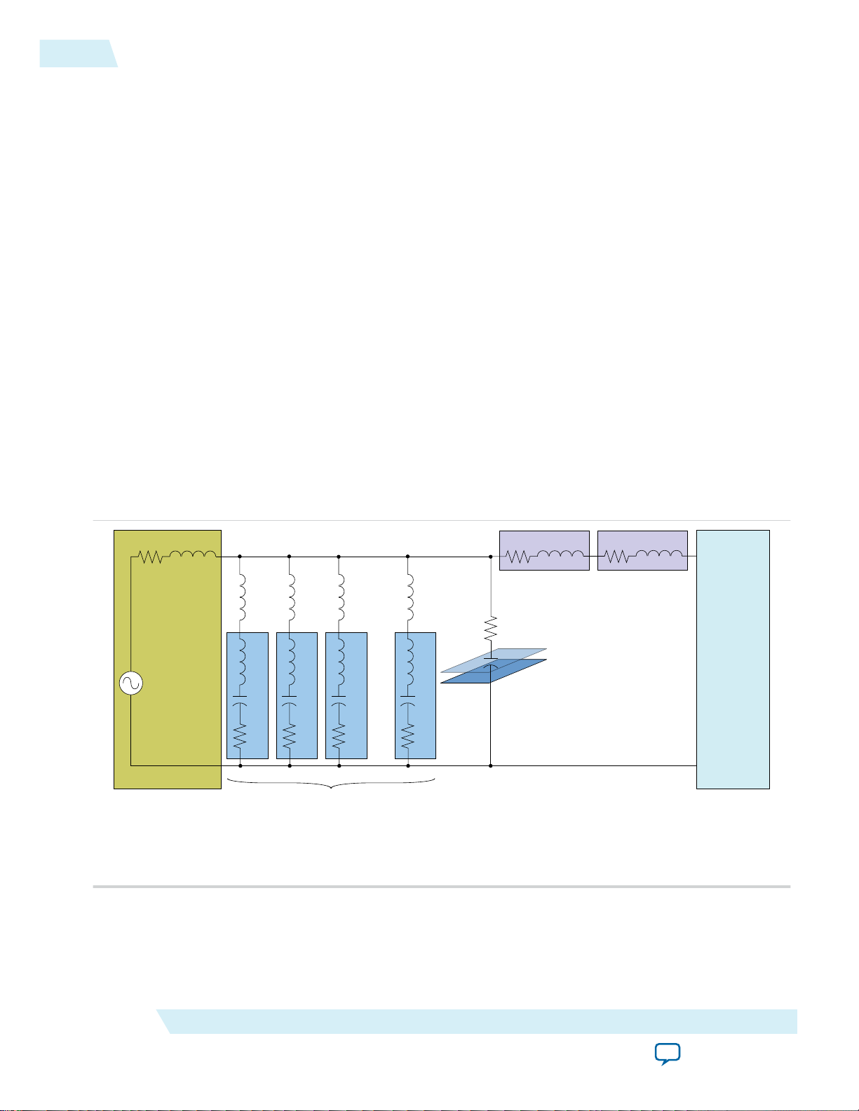
Lc1
Cc1
Rc1
Lmnt1
Lc2
Cc2
Rc2
Lmnt2
Lc3
Cc3
Rc3
Lmnt3
Lc N
Cc N
Rc N
Lmnt N
Rp
Cp
Planar
R and C
(4)
Rs Ls
Rv Lv
Spreading R and L
(3)
BGA Via R and L
(3)
Rvrm Lvrm
VRM Model
(1)
Decoupling CAP Model
(2)
Altera
FPGA Device
VRM
Notes:
1. You can define or change VRM parameters in the Library sheet of the PDN tool.
2. You can define or change Decoupling CAPs parameters in the Cap Mount, X2Y Mount, and Library sheets of the PDN tool.
3. Rs and Ls are parasitic capacitances and inductances from BGA balls and PCB traces and connections.
4. Represents PCB layers dedicated to power and ground planes.
2
PDN Decoupling Methodology Review
The device families supported by the Altera device-specific PDN tool 2.0 are shown at the top of the
Release Notes tab and they include:
• Arria® 10
• Arria V
• Arria II GZ
• Cyclone® V
• Cyclone IV E
• Cyclone IV GX
• Stratix® V
• MAX® 10
PDN Decoupling Methodology Review
UG-01157
2015.03.06
The PDN tool 2.0 provides two parameters for guiding PCB decoupling design: Z
PDN Circuit Topology
The PDN tool 2.0 is based on a lumped equivalent model representation of the power delivery network
topology.
Figure 1: PDN Topology Modeled as Part of the Tool
The PDN impedance profile is the impedance-over-frequency looking from the device side.
TARGET
and F
EFFECTIVE
.
Altera Corporation
Device-Specific Power Delivery Network (PDN) Tool 2.0 User Guide
Send Feedback
Page 3

Z
TARGET
=
Voltage Rail ×
100
Die Noise Tolerance%
( )
Maximum Dynamic Current Change
Z
TARGET
=
2 × 0.5
0.09 Ω
=
1.8 × 0.05
UG-01157
2015.03.06
Z
TARGET
3
For first order analysis, the VRM can be simply modeled as a series-connected resistor and inductor as
shown above. The VRM has a very low impedence and can respond to the instantaneous current require‐
ments of the FPGA in the following circumstances:
• At low frequencies up to approximately 50 KHz
• Depending on the voltage regulation module you use
The equivalent series resistance (ESR) and equivalent series inductance (ESL) values can be obtained from
the VRM manufacturer. At higher frequency, the VRM impedance is primarily inductive, making it
incapable of meeting the transient current requirement.
PCB decoupling capacitors are used for reducing the PDN impedance up to 100-150 MHz. The on-board
discrete decoupling capacitors provide the required low impedance. This depends on the capacitorintrinsic parasitics (RcN, CcN, LcN) and the capacitor mounting inductance (L
). The inter-planar
mntN
capacitance between the power-ground planes typically has lower inductance than the discrete decoupling
capacitor network, making it more effective at higher frequencies up to 150 MHz. As frequency increases,
the PCB decoupling capacitors become less effective. The limitation comes from the parasitic inductance
seen with respect to the FPGA. FPGA parasitic inductance includes capacitor mounting inductance, PCB
spreading inductance, ball grid array (BGA) via inductance, and packaging parasitic inductance. All of
these parasitics are modeled in the PDN tool 2.0 to capture the effect of the PCB decoupling capacitors
accurately. To simplify the circuit topology, all parasitics are represented with lumped inductors and
resistors despite the distributed nature of PCB spreading inductance.
Z
TARGET
Figure 2: Z
Figure 3: Z
According to Ohm’s law, voltage drop across a circuit is proportional to the current flow through the
circuit, and impedance of the circuit. The dynamic component of PDN current gives rise to voltage
fluctuation within the PDN, which may lead to logic and timing issues. You can reduce excessive voltage
fluctuation by reducing PDN impedance. One design guideline is target impedance, Z
TARGET
. Z
TARGET
defined using the maximum allowable die noise tolerance and dynamic current change, and is calculated
as follows.
Equation
TARGET
For example, to reliably decouple a 1.8-volt power rail that allows 5% of die noise tolerance and a
maximum 2 A current draw, 50% of which is dynamically changing, the desired target impedance is
calculated as follows.
Example Equation
TARGET
is
Device-Specific Power Delivery Network (PDN) Tool 2.0 User Guide
Send Feedback
Altera Corporation
Page 4
4
Z
TARGET
UG-01157
2015.03.06
To accurately calculate the Z
TARGET
for any power rail, you must know the following information:
• The maximum dynamic current change requirements for all devices in the system that are powered by
the power rail under consideration. You can obtain this information from manufacturers of the
respective devices. You can calculate the maximum dynamic current change of a device using the
maximum total current and the dynamic current change percentage.
Note: The dynamic current change is intended to parameterize the high-frequency current draws
required to provide the energy for CMOS transistors changing state. In the case of the core rail,
the transients are generated by switching inside the FPGA core. Thus, a design which involves
extensive logical switching generates higher % transients (dynamic current change) than a more
static design. For information about recommended settings, refer to the table in the Introduc‐
tion tab of the PDN tool 2.0.
Note: You can obtain accurate estimations on the maximum total current for Altera devices using the
Altera PowerPlay Early Power Estimator (EPE) tool or the Quartus® II PowerPlay Power
Analyzer tools.
• The maximum allowable die noise tolerance on the power rail is given as a percentage of the supply
voltage.
Device switching activity leads to transient noise (high frequency spikes) seen on the power supply rails.
This noise can cause functionality issues if they are too high. The noise must be damped within a range
defined as a percentage of power supply voltage. The recommended values for the maximum allowable
AC die noise tolerance are listed in the Introduction tab of the PDN tool 2.0. Different rails have different
specifications because of their sensitivity to the transient voltage noise as well as how much current is used
by the power rail.
This AC die noise tolerance differs from the minimum and maximum voltage specifications in the device
datasheet in that the voltage specifications in the device datasheet are DC values. The (DC) ripple of the
voltage regulator module (VRM) is the change in the power supply voltage level. Altera devices are
designed to operate within a specific voltage range, which is considered the DC specification. The DC
specification is, in turn, translated to the requirement for the VRM ripple specification. This DC specifica‐
tion is not included in the die noise tolerance field in the PDN tool 2.0.
Refer to the Introduction tab of the PDN tool 2.0 for more information about Z
TARGET
.
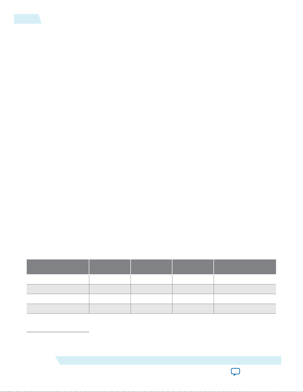
Table 2: Settings for the Arria 10 Device Power Rails
This information is from the PDN tool 2.0 for an Arria 10 device.
Rail Name
(1)
Voltage (V) Die Noise
Tolerance (%)
Dynamic Current
Change (%)
Description
VCC 0.85 - 0.9 5 50 Core
VCCIO 1.2 - 3.0 5 100 I/O Bank
VCCPT 1.8 5 50 I/O Pre-Drivers
VCCPGM 1.2/1.5/1.8 5 50 Programming Power
(1)
For more information about power rail functions, refer to the Pin Connection Guidelines for the selected
device family.
Altera Corporation
Device-Specific Power Delivery Network (PDN) Tool 2.0 User Guide
Send Feedback
Page 5
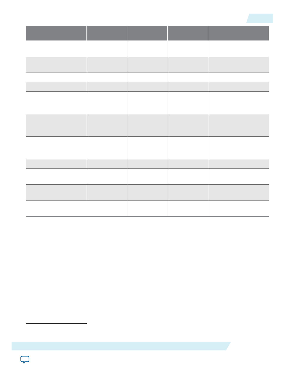
UG-01157
2015.03.06
Z
TARGET
5
Rail Name
(1)
Voltage (V) Die Noise
Tolerance (%)
Dynamic Current
Change (%)
Description
VCCERAM 0.95 5 50 Programmable Power
Tech Aux
VCCBAT 1.2/1.5/1.8 5 100 Battery Back-up Power
Supply
VCCA_PLL 1.8 5 10 PLL (Analog)
VCCA_FPLL 1.8 5 10 FPLL
VCCR_GXB 0.9/1.0/1.1 3 30
XCVR
RX (Analog)
VCCT_GXB 0.9/1.0/1.1 2 60
XCVR
TX (Analog)
VCCA_GXB 0.9/1.0/1.1 5 10
XCVR
/CDB (Analog)
VCCH_GXB 0.9/1.0/1.1 3 15 XCVR I/O Buffer Block
VCCR_GTB 0.9/1.0/1.1 3 30 28 Gbps XCVR RX
(Analog)
VCCT_GTB 0.9/1.0/1.1 2 60 28 Gpbs XCVR TX
(Analog)
VCCP 0.9 5 33 Periphery Supply
Voltage
Related Information
• Altera PowerPlay Early Power Estimator (EPE)
• Arria 10 GX, GT, and SX Device Family Pin Connection Guidelines.
• MAX 10 Device Family Pin Connection Guidelines.
• Stratix V E, GS, and GX Device Family Pin Connection Guidelines.
• Stratix V GT Device Family Pin Connection Guidelines.
• Arria V GT, GX, ST, and SX Device Family Pin Connection Guidelines.
• Arria II Device Family Pin Connection Guidelines.
• Cyclone V Device Family Pin Connection Guidelines.
• Cyclone IV Device Family Pin Connection Guidelines.
(1)
For more information about power rail functions, refer to the Pin Connection Guidelines for the selected
device family.
Device-Specific Power Delivery Network (PDN) Tool 2.0 User Guide
Send Feedback
Altera Corporation
Page 6
6
F
EFFECTIVE
F
EFFECTIVE
UG-01157
2015.03.06
As previously illustrated, a capacitor reduces PDN impedance by providing a least-impedance route
between power and ground. Impedance of a capacitor at high frequency is determined by its parasitics
(ESL and ESR). For a PCB-mount capacitor, the parasitics include not only the parasitic from the
capacitors themselves but also those associated with mounting, PCB spreading, and packaging. Therefore,
PCB capacitor parasitics are generally higher than those of on-package decoupling capacitor and on-diecapacitance. Decoupling using PCB capacitors becomes ineffective at high frequency. Using PCB
capacitors for PDN decoupling beyond their effective frequency range brings little improvement to PDN
performance and raises the bill of materials (BOM) cost.
To help reduce over-design of PCB decoupling, this release of the PDN tool provides a suggested PCB
decoupling design cut-off frequency (F
EFFECTIVE
package, and die parasitics. You only need to design PCB decoupling that keeps Z
F
EFFECTIVE
.
) as another guideline. It is calculated using the PCB,
under Z
EFF
TARGET
up to
Refer to Troubleshooting Z
EFF
if the Z
too high.
Note: F
EFFECTIVE
may not be enough when the Altera FPGA device shares a power rail with another
device. The noise generated from other devices propagates along the PDN and affects FPGA device
performance. The frequency of the noise is determined by the transfer impedance between the
noise source and the FPGA device, and can be higher than F
inductance and increasing the isolation between the FPGA device and noise source reduces this
risk. You must perform a transfer impedance analysis to clearly identify any noise interference risk.
Related Information
• Troubleshooting ZEFF on page 27
• For more information about the PDN decoupling methodology behind the Altera PDN design
tool, refer to the Power Distribution Network Design Using Altera PDN Design Tools online
course.
Major Tabs of the PDN Tool 2.0
The tabs at the bottom of the PDN tool 2.0 application help you calculate your impedance profile.
Table 3: PDN Tool 2.0 Tabs
Tab Description
is too high or the number of capacitors for decoupling becomes
EFF
EFFECTIVE
. Reducing PDN parasitic
Release_Notes Provides the legal disclaimers, the revision history of the tool,
Introduction
Altera Corporation
and the user agreement.
Displays the schematic representation of the circuit that is
modeled as part of the PDN tool 2.0. It also provides the
following related information:
• a quick start instruction
• recommended settings for some power rails
• a brief description of decoupling design procedures under
different power supply connection schemes
Device-Specific Power Delivery Network (PDN) Tool 2.0 User Guide
Send Feedback
Page 7

UG-01157
2015.03.06
System_Decap
Tab Description
System_Decap The principal tab that allows you to decouple your system. It
displays by default when you launch the application. This tab
provides an interface to enter your power sharing scheme for a
selected FPGA device and derive the decoupling based on the
input.
Stackup Provides an interface to enter your stackup information into the
PDN tool.
Library Points to various libraries (capacitor, dielectric materials, and so
on) that are called by other tabs. You can change the default
values listed as part of these libraries.
BGA_Via Provides an interface to calculate the BGA mounting inductance
based on design-specific via parameters and the number of vias.
Plane_Cap Provides an interface to calculate the plane capacitance based on
design-specific parameters.
Cap_Mount Provides an interface to input design-specific parameters for
calculating the capacitor mounting inductance for two different
capacitor orientations (Via on Side [VOS] and Via on End
[VOE]).
7
X2Y_Mount Provides an interface to input design-specific parameters for
calculating the capacitor mounting inductance for X2Y type
capacitors.
Enlarged_Graph Provides an enlarged view of the Z-profile shown in the System_
Decap tab.
System_Decap
You can determine the decoupling of selected FPGA devices based on the power sharing scheme entered
in the System_Decap tab.
The System_Decap tab is divided into the following sections:
• Device selection
• Power rail data and configuration
• VRM Data
• Rail group summary
• VRM Impedance
• BGA Via
• Plane
• Spreading
• F
EFFECTIVE
• Decoupling selection
• Result summary
Device-Specific Power Delivery Network (PDN) Tool 2.0 User Guide
Send Feedback
Altera Corporation
Page 8
8
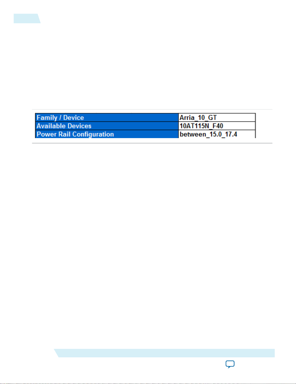
Device Selection Section
Device Selection Section
1. Select the Family/Device using the pull-down list.
2. Select your device from the Available Devices pull-down list.
3. Select your desired power rail configuration from the Power Rail Configuration pull-down list.
The pull-down selections are based on examples from the pin connection guidelines for the device. Select
the closest one to your design, and use it as a basis for entering your design data. Refer to the pin
connection guidelines for your device on the Altera website.
The tool updates the list of power rails and the contents in the power rail configuration sections based on
your selections.
Figure 4: Device Selection
Related Information
UG-01157
2015.03.06
• Arria 10 GX, GT, and SX Device Family Pin Connection Guidelines.
• MAX 10 Device Family Pin Connection Guidelines.
• Stratix V E, GS, and GX Device Family Pin Connection Guidelines.
• Stratix V GT Device Family Pin Connection Guidelines.
• Arria V GT, GX, ST, and SX Device Family Pin Connection Guidelines.
• Arria II Device Family Pin Connection Guidelines.
• Cyclone V Device Family Pin Connection Guidelines.
• Cyclone IV Device Family Pin Connection Guidelines.
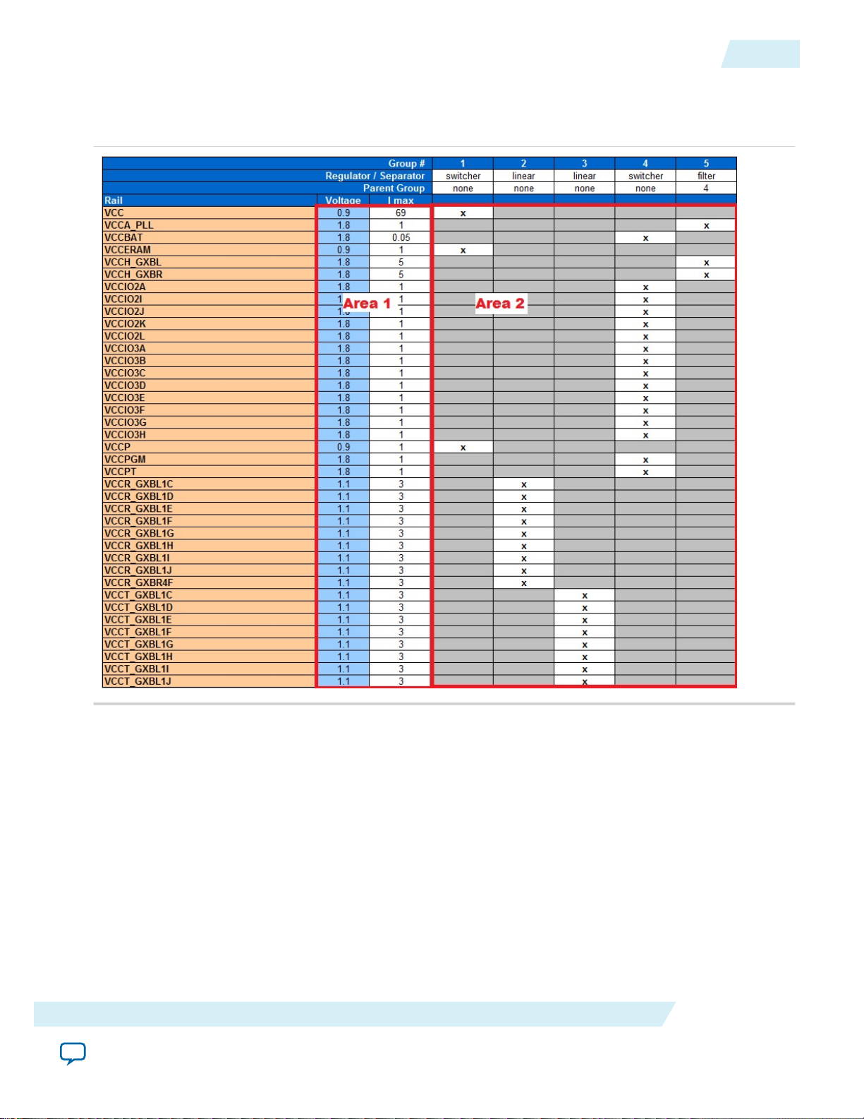
Power Rail Data and Configuration Section
This section of the application is divided into two areas. Area 1 is for the device power rail information,
and Area 2 is for the power rail configuration.
1. Enter the power supply voltage in the Voltage column for each power rail listed in Area 1 by selecting
a value from the pull-down menu, or by manually entering your own value.
Note:
You must enter the total current consumption of related power rails before you can use the
system decoupling function.
You can optionally adjust the recommended number up or down slightly based on knowledge of the
intended application.
2. Enter the current consumption in the I max column for each power rail.
The earliest data from the Altera PowerPlay Early Power Estimator (EPE) can provide good values for
the current entries. The EPE delivers bulk data for the transceiver channels. Each bank of transceiver
channels should be assigned the total EPE value divided by the number of banks. Later in the design
cycle, the Quartus II Power Play Power Analyzer (PPPA) can derive much better data for each bank
rail.
3. Setup your device power sharing scheme in Area 2.
Altera Corporation
Device-Specific Power Delivery Network (PDN) Tool 2.0 User Guide
Send Feedback
Page 9
UG-01157
2015.03.06
Power Rail Data and Configuration Section
Figure 5: Power Rail Data and Power Sharing Scheme Section
This configuration is an example of how this section of the spreadsheet should look. Every design will
vary slightly.
9
Each column in Area 2 represents a power group in your system. Add or remove a power group using
the Add Group or Remove Group buttons. The first row of each group is the Regulator/Separator
type. Set the source type for the power group and available options from the pull-down list as switcher,
linear, or filter.
The second row is the Parent Group type. The available options for this row are None and the number
representing all listed power groups. Input your power sharing hierarchy in this column, and set the
power rail connection using the remaining rows.
Note:
The PDN tool 2.0 defines the power rail configuration using the Parent/Child power group. A
power group is a child power group if it attaches to another power group. The other power
group is the parent group in this case. A parent group can have multiple child groups. A parent
power group number is required for the child group. The parent group number of a parent
power group is assigned to None because the group has no parent group.
Device-Specific Power Delivery Network (PDN) Tool 2.0 User Guide
Send Feedback
Altera Corporation
Page 10

10
VRM Data Section
The available options are:
• " " — Device rail does not connect to the power group.
• x — Device rail connects to the power group.
• x/related— Device rail connects to the group, and its activity is related to other rails that connect to
Note: Two IO rails are related if their output activities are synchronous. For example, when two
The PDN tool 2.0 sets the default power rail sharing configuration based on the selected Alterarecommended power rail configuration listed above. Make changes to better match your design.
Related Information
Altera PowerPlay Early Power Estimator (EPE)
VRM Data Section
UG-01157
2015.03.06
the same group. You must select x/related if that VCCIO/VCCPT power rail is related to other rails
within the same power rail group.
VCCIO rails are assigned to the same memory interface. The maximum current will usually be
reached at the same time for these related rails. As a result, the total current of related rails
equals the sum of the current of all shared rails. The total current of unrelated rails is calculated
using the root-mean-square (RMS) method.
Enter the voltage regulator module (VRM) parameters for DC supply voltage at Switcher VRM
Efficiency and Switcher VRM Input Current.
Rail Group Summary Section
In this section, you can find a list of the following calculated key parameters of all power groups:
• Voltage
• Total Current
• Dynamic Current Change
• Die Noise Tolerance
• Core Clock Frequency
• Current Ramp Up Period
• Z
TARGET
These options allow you to customize how the data is collected or analyzed.
The Dynamic Current Change parameter has a pull-down menu with the following options:
• Calculate
• Override
Dynamic current change percentage requires a lot of diligence. The EPE and PPPA both deliver values for
current usage that include:
• the maximum static current (does not vary)
• the maximum current usage by the active elements
This calculation yields both a very high total current and a fairly high dynamic current usage. Calculations
for a value to insert into the Dynamic Current Change field could yield a value much lower than the
auto-populated value, which represents a safe engineering value.
Altera Corporation
Device-Specific Power Delivery Network (PDN) Tool 2.0 User Guide
Send Feedback
Page 11

UG-01157
2015.03.06
VRM Impedance Section
11
The Die Noise Tolerance parameter has a pull-down menu with the following options:
• Calculate
• Override
Some PDN tool variants allow you to add data for the Core Clock Frequency and Current Ramp Up
Period parameters using the pull-down menus. These values tell the tool how to calculate the current
ramp up period for transient events, sometimes reducing transient current changes. The values relate to
how fast the clock for the section is running, and the length of the data pipeline. Given a transient change
in the input data, there are clock cycles in the pipeline for the algorithm to deliver the results. If the input
data change activates a broad yet short pipeline, the transient is abrupt. This results in a large current
change for the number of logic elements being used. If the pipeline is narrow and long, the overall change
in current usage is proportionately smaller.
You can set the Core Clock Frequency parameter to a High, Medium, Low, or Custom set of input
frequencies. The Custom option allows you to enter a specific input frequency.
The Current Ramp Up Period parameter allows you to specify the number of clock cycles consumed by
the pipeline. You can select a High, Medium, Low, or Custom setting. Altera recommends using a
smaller value unless you have already entered a complete design in Quartus II and determined the precise
value.
VRM Impedance Section
Enter the VRM impedance values for the regulators. Use the pull-down menu to enter data for VRM
Resistance and VRM Inductance.
There are three ways to change the voltage regulator module (VRM) parameters. Depending on what you
select in the VRM Impedence pull-down menu, you can:
• Select Custom and set your desired Rvrm and Lvrm values.
• Select Library and get the suggested typical Rvrm and Lvrm values. This depends on the type of
regulator (for example, switching, linear, or filter) you have selected.
• For switching regulators, you can choose a specific Enpirion® VRM (based on ordering code) directly
in the pull-down menu.
You can use the PowerPlay Early Power Estimator (EPE) to help select the appropriate Enpirion VRM
module to use for each power supply in your system.
BGA Via Section
In the BGA Via table shows the L and R values per via. You can set the tool to Calculate, Custom, or
Ignore. For a fully customized workflow in which each rail group can have different settings:
1. Select the System_Decap tab in the PDN tool 2.0.
2. Set the total effective R and L values in the BGA Via section to match your system.
Setting the BGA Via table to Calculate or Ignore causes the System_Decap tab to use the same global
settings for all rail groups.
Plane Section
In the Plane table, you can set the tool to Calculate, Custom, or Ignore. For a fully customized workflow
in which each rail group can have different settings:
Device-Specific Power Delivery Network (PDN) Tool 2.0 User Guide
Send Feedback
Altera Corporation
Page 12

12
Spreading Section
1. Select the Plane_Cap tab in the PDN tool 2.0.
2. Set the parameters to match your system, and notice that the Total planar capacitance and Total
sheet resistance values are updated automatically .
3. In the System_Decap tab, select the Custom option for each group where a custom plane is required.
4. Enter the calculated Ctotal and Rtotal values into the Plane section of the System_Decap tab.
Setting the Plane table to Calculate or Ignore causes the System_Decap tab to use the same global
settings for all rail groups.
Spreading Section
In the Spreading table, you can set the tool to one of the following options:
• Ignore
• Low
• Medium
• High
• Custom
For a fully customized workflow in which each rail group can have different settings:
1. Select the Library tab in the PDN tool 2.0.
2. Set the parameters in the Spreading R and L table to match your system.
3. Examine the range of spreading R and L values to determine if you need a custom R and L. If a custom
R and L is warranted, select Custom in the System_Decap tab and set the R and L values directly.
UG-01157
2015.03.06
Setting the Spreading table to Low, Medium, High, or Ignore causes the System_Decap tab to use the
same global settings for all rail groups.
F
EFFECTIVE
Section
You can set Feffective to Calculate or Override. Select the Calculate option to use the Altera
recommended cut off frequency based on package and die parasitics.
Decoupling Section
You can set Decoupling to Manual or Auto. If you select the Auto option, any change you make to the
system is automatically reflected in the decoupling solution. You can also view the impedance chart per
rail group or VRM.
Selecting the Manual option allows you to:
• Lock in calculated decoupling solutions from being further optimized by any changes made to the
System_Decap tab.
• Add or remove the number and type of decoupling capacitors in the Results Summary section. You
can see its immediate impact on the impedance profile curve.
Results Summary Section
You can find the list of the number and type of capacitors used for each group, and the summary of all the
capacitors used. The values in each column indicate the number of capacitors needed of each value for
each rail.
Altera Corporation
Device-Specific Power Delivery Network (PDN) Tool 2.0 User Guide
Send Feedback
Page 13
UG-01157
2015.03.06
Recommended Flow for Deriving Decoupling for FPGA System using the
System_Decap Tab
Figure 6: Results Summary Section of the System_Decap Tab
Recommended Flow for Deriving Decoupling for FPGA System using the System_Decap Tab
To use the System_Decap tab, perform the following steps:
13
Stackup
1. Select the Altera device family or device.
2. Set up the stack up information in the Stackup tab.
3. Select the decoupling scheme.
The tool updates the power rail connection configuration to the scheme recommended in the Pin
Connection Guidelines.
4. Ensure that the following default parameters match your system, and make the necessary changes such
as:
• power rail configuration
• relativity of power rails within the same power group
• power group layer
• number of power/ground Via pairs
• DC voltage supply for VRM module
• decoupling cap location
5. Enter the projected current consumption of each power rail.
If you applied the Custom setting, refer to BGA Via Section on page 11, Plane Section on page 11, or
Spreading Section on page 12 to enter your values.
Enter the PCB stackup information of your design in the Stackup tab. This tab updates related data in the
BGA_Via, Plane_Cap, Cap_Mount and the X2Y_Mount tabs. The stackup information in this tab is also
used for the System_Decap tab. Follow the instructions provided at the beginning of the tab to fill in the
content for this tab.
Device-Specific Power Delivery Network (PDN) Tool 2.0 User Guide
Send Feedback
Altera Corporation
Page 14

14
Stackup Data
Figure 7: Stackup Tab
UG-01157
2015.03.06
Stackup Data
The Stackup Data section is where you enter board dimension data and other parameters, such as board
stackup settings, power via, and dielectric material.
Stackup Stub
The content in this section is updated based on the settings in Stackup Configuration, in the Stackup
Data section. Enter the thickness of the metal/dielectric material for each layer. The stackup shown in this
section is used as the basic unit to construct the complete PCB stackup.
Full Stackup
This section lists the complete stackup of your board. You can modify content in the section to better
match your board design. The last column in the section is the PWR plane types. In a single rail analysis
case, assign the layer where the power rail is located as target, and the ground layer that the power rail
refers to as reference.
Altera Corporation
Device-Specific Power Delivery Network (PDN) Tool 2.0 User Guide
Send Feedback
Page 15
UG-01157
2015.03.06
Table 4: Full Stackup Buttons
Button Label Description
Construct Stackup Populates the Full Stackup section to the number of layers
Import Geometries Updates geometry parameters in the BGA_Via, Plane_Cap,
Proceed to System Decap Opens the System_Decap tab.
BGA_Via
The BGA Via tab calculates the vertical via loop inductance under the BGA pin field.
BGA_Via
defined in the Stackup Data section using the blocks listed in
the Stackup Stub section.
Cap_Mount, and X2Y_Mount tabs using your input from the
Stackup Data section. The tool also checks that the PWR
Planes column in the Full Stackup section has only one target
layer, and provides a warning for this error.
15
Device-Specific Power Delivery Network (PDN) Tool 2.0 User Guide
Send Feedback
Altera Corporation
Page 16

16
Plane_Cap
Figure 8: BGA_Via Tab
The values in the Unit column indicate a unit value per one pair.
UG-01157
2015.03.06
Enter the layout-specific information such as via drill diameters, via length, via pitch, and the number of
power/ground via pairs under the BGA in the BGA Via Inductance table. The tool calculates the effective
via loop inductance and resistance value. You can save the change made to the tab, restore the changes, or
restore the tab back to the default settings.
Plane_Cap
The Plane Cap tab calculates the distributed plane capacitance in microfarads (µF) that is developed
between the power/ground planes based on the parallel plate capacitor equation.
Altera Corporation
Device-Specific Power Delivery Network (PDN) Tool 2.0 User Guide
Send Feedback
Page 17

UG-01157
2015.03.06
Figure 9: Plane_Cap Tab
Cap_Mount
17
Enter the design specific information such as plane dimensions, plane configuration and the dielectric
material used in the Planar Capacitance table. The tool calculates a plane capacitance value. You can save
custom values, restore custom values, or restore the default settings.
Cap_Mount
The Cap Mount tab calculates the capacitor mounting inductance seen by the decoupling capacitor.
Note:
Device-Specific Power Delivery Network (PDN) Tool 2.0 User Guide
Send Feedback
Power rails on different layers have different mounting inductances. For the best results, run the
PDN separately for each layer set.
Altera Corporation
Page 18
18
X2Y_Mount
Figure 10: Cap Mount Tab
UG-01157
2015.03.06
The capacitor mounting calculation is based on the assumption that the decoupling capacitor is a twoterminal device. The capacitor mounting calculation is applicable to any two-terminal capacitor with the
following footprints: 0201, 0402, 0603, 0805, and 1206. Enter all the information relevant to your layout,
and the tool provides a mounting inductance for a capacitor mounted on either the top or bottom layer of
the board. Depending on the layout, you can choose between VOE (Via on End) or VOS (Via on Side) to
achieve an accurate capacitor mounting inductance value.
If you plan to use a footprint capacitor other than a regular two-terminal capacitor or X2Y capacitor for
decoupling, you can skip the Cap Mount tab. In this case, you can directly enter the capacitor parasitics
and capacitor mounting inductance in the Library tab (under the Custom field in the Decoupling Cap
section of the library). As with the other tabs, you can save the changes made to the tab, restore the
changes, or restore the tab back to the default settings.
X2Y_Mount
The X2Y Mount tab calculates the capacitor mounting inductance seen by the X2Y decoupling capacitor.
Altera Corporation
Device-Specific Power Delivery Network (PDN) Tool 2.0 User Guide
Send Feedback
Page 19

UG-01157
2015.03.06
Figure 11: X2Y_Mount Tab
Library
19
Enter all the information relevant to your layout in the X2Y CAP Mounting Inductance table. The tool
then provides a mounting inductance for an X2Y capacitor mounted on either the top or bottom layer of
the board. You can save the changes made to the tab, restore the changes, or restore the tab back to the
default settings.
Library
The Library tab stores all the device parameters that are referred to in the other tabs.
Device-Specific Power Delivery Network (PDN) Tool 2.0 User Guide
Send Feedback
Altera Corporation
Page 20

20
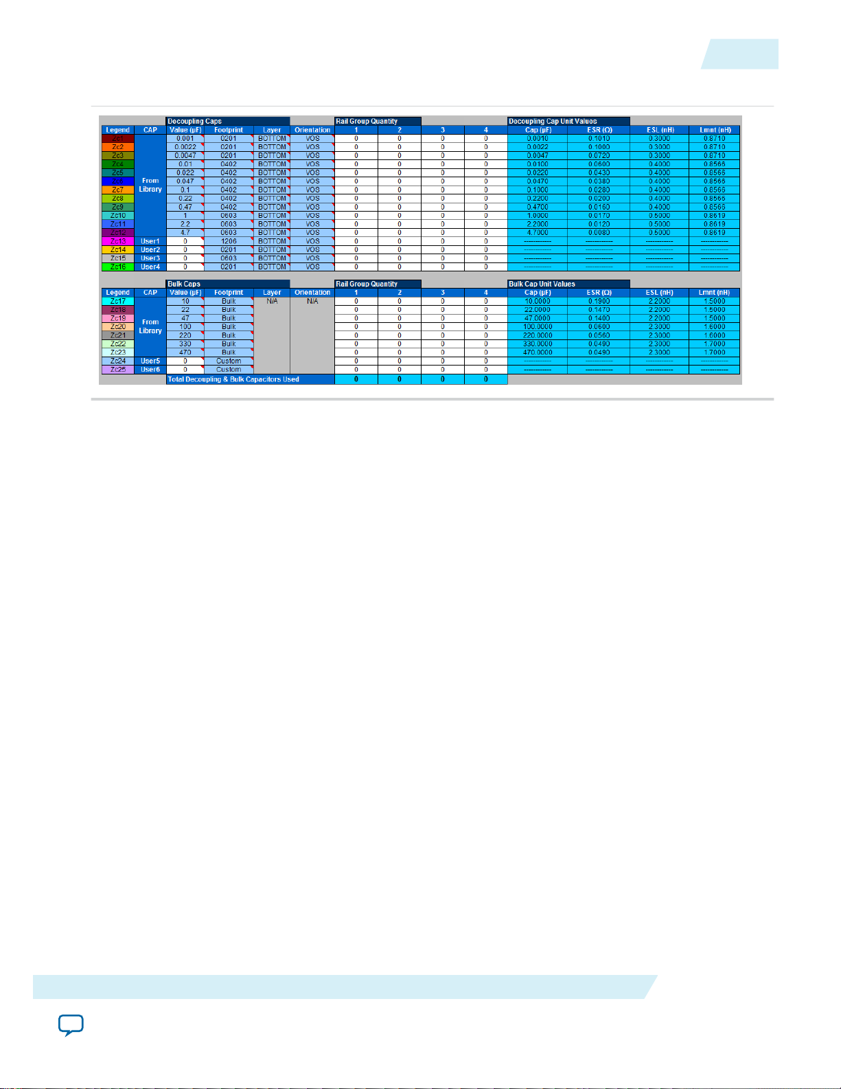
Two-Terminal Decoupling Capacitors
Figure 12: Library Tab
UG-01157
2015.03.06
You can change each of the default values listed in the respective sections to meet the specific needs of
your design.
Two-Terminal Decoupling Capacitors
The decoupling capacitors section contains the default ESR and ESL values for the various two-terminal
capacitors in the following footprints:
Altera Corporation
Device-Specific Power Delivery Network (PDN) Tool 2.0 User Guide
Send Feedback
Page 21

UG-01157
2015.03.06
Bulk Capacitors
• 0201
• 0402
• 0603
• 0805
• 1206
You also have the option to either modify the default values or enter your own commonly used custom
values in the Custom field. If you are using a capacitor with a footprint that is not available in the tool,
you must use the Custom field to enter the capacitor parasitics and the corresponding mounting
inductance.
The decoupling capacitors section also provides the option for the user defined capacitors (such as
User1,...,User4). You can define the ESR and ESL parasitics for the various footprints and enter the
corresponding capacitor value in the System_Decap tab. Choose the corresponding footprint when
defining the capacitor values.
Bulk Capacitors
The bulk capacitors section contains the commonly used capacitor values for decoupling the power
supply at mid and low frequencies. You can change the default values to reflect the parameters specific to
the design.
21
X2Y Decoupling Capacitors
The X2Y decoupling capacitors section contains the default ESR and ESL values for the various X2Y
capacitors in the 0603, 0805, 1206, and 1210 footprints. You also can replace the default ESR and ESL
values with your own commonly used custom values.
BGA Via and Plane Capacitance
This section allows you to directly enter the values for effective via loop inductance under the BGA and
plane capacitance during the pre-layout phase when no design-specific information is available.
If you have access to design-specific information, you can ignore this section and enter the design-specific
information in the Plane Cap and BGA Via tabs that calculate the plane capacitance and the BGA via
parasitics, respectively.
VRM Library
The VRM section lists the default values for both the linear and switcher regulators. In the Custom field,
you can change the VRM parasitics listed under the linear/switcher rows or add the custom parasitics for
the VRM relevant to the design.
Spreading R, L Parasitics
This library provides various options for the default effective spreading inductance values that the
decoupling capacitors see with respect to the FPGA. These values are based on the quality of the PDN
Device-Specific Power Delivery Network (PDN) Tool 2.0 User Guide
Send Feedback
Altera Corporation
Page 22

22
Dielectric Material Library
design. You can choose a Low value of effective spreading inductance if you have optimally designed your
PDN Network. Optimum PDN design involves implementing the following design rules:
• PCB stackup that provides a wide solid power/ground sandwich for a given supply with a thin
dielectric between the planes. This minimizes the current loop, which reduces the spreading
inductance. The thickness of the dielectric material between the power/ground pair directly influences
the amount of spreading/loop inductance that a decoupling cap can see with respect to the FPGA.
• Placing the capacitors closer to the FPGA from an electrical standpoint.
• Minimizing via perforations in the power/ground sandwich in the current path from the decoupling
caps to the FPGA device.
Due to layout and design constraints, the PDN design may not be optimal. In this case, you can choose
either a Medium or High value of spreading R and L. You can also change the default values or use the
Custom field listed in the library specific to the design.
Dielectric Material Library
This library lists the dielectric constant values for the various commonly used dielectric materials. These
values are used in the plane capacitance calculations listed under the Plane_Cap tab. You can change the
values listed in this section.
If you change the default values listed in the various sections in the Library tab, you can save the changes
by clicking Save Custom. You can restore the default library by clicking Restore Default located at the
top right-hand corner of the Library page. You can also restore the saved custom library by clicking
Restore Custom.
UG-01157
2015.03.06
User Set F
EFFECTIVE
You must decouple to a F
device families. In this case, you must set the F
The PDN tool 2.0 then uses the F
Enlarged_Graph
In the Enlarged_Graph tab, you can view the enlarged Z-profile plot. The PDN tool 2.0 switches to this
tab when you click on the Z-profile plot in the System_Decap tab. You can go back to the System_Decap
tab when you click the Return button.
EFFECTIVE
EFFECTIVE
higher than what is calculated for the power rails of some Altera
EFFECTIVE
option to Override in the System_Decap tab.
value entered here.
Altera Corporation
Device-Specific Power Delivery Network (PDN) Tool 2.0 User Guide
Send Feedback
Page 23

UG-01157
2015.03.06
Figure 13: Enlarged_Graph Tab
Design PCB Decoupling Using the PDN Tool 2.0
23
Design PCB Decoupling Using the PDN Tool 2.0
PCB decoupling keeps PDN Z
tion up to the frequency where the capacitor on the package and die take over the PDN decoupling. This
procedure uses the PDN tool 2.0 in different power rail configurations and provides design examples
using the Arria 10 device PDN tool.
Pre-Layout Instructions
The PDN tool 2.0 provides an accurate estimate of the number and types of capacitors needed to design a
robust power delivery network, regardless of where you are in the design phase. However, the accuracy of
the results depends highly on the user inputs for the various parameters.
If you have finalized the board stackup and have access to board database and layout information, you can
proceed through the tabs and enter the required information to arrive at an accurate decoupling scheme.
Device-Specific Power Delivery Network (PDN) Tool 2.0 User Guide
Send Feedback
smaller than Z
EFF
TARGET
with the properly chosen PCB capacitor combina‐
Altera Corporation
Page 24

24
Pre-Layout Instructions
In the pre-layout phase of the design cycle when you do not have specific information about the board
stack-up and board layout, you can follow these instructions to explore the solution space when finalizing
key design parameters such as stackup, plane size, capacitor count, capacitor orientation, and so on.
In the pre-layout phase, ignore the Plane Cap and Cap Mount tabs and go directly to the Library tab
when you do not have the layout information. If available, enter the values shown below in the Library
tab. To use the default values, go directly to the System_Decap tab to begin the analysis.
Figure 14: Library Tab Fields
The callouts correspond to the fields in which you must enter values.
UG-01157
2015.03.06
Altera Corporation
Device-Specific Power Delivery Network (PDN) Tool 2.0 User Guide
Send Feedback
Page 25

UG-01157
2015.03.06
1. Enter the ESR, ESL, and Lmnt values for the capacitors listed in the Custom field.
2. Enter the effective BGA via (loop) parasitics for the power supply being decoupled in the BGA Via &
Plane Cap field..
3. Enter the plane capacitance seen by the power/ground plane pair on the board for the power supply in
the BGA Via & Plane Cap field.
4. Enter the VRM parasitics, if available, in the Custom row of the VRM field.
5. Enter the effective spreading inductance seen by the decoupling capacitors in the Custom row of the
Spreading R and L field.
Deriving Decoupling in a Single-Rail Scenario
A power supply connects to only one power rail on the FPGA device in a single-rail scenario. The PDN
noise is created by the dynamic current change of the single rail. You determine Z
based on the parameters related to the selected rail only.
The PDN tool 2.0 provides two ways to derive a decoupling network. You can set up the tool with the
information needed and let the tool derive the PDN decoupling for your system. You can also manually
enter the information and derive decoupling. To derive the desired capacitor combination:
1. Select the device/power rail to work with.
2. Select the parameter settings for the PDN components.
3. Enter the electric parameters to set Z
You need to have a good estimate of the parameters entered to derive the proper decoupling guidelines
(Z
TARGET
scenario, pessimistic settings result in hard-to-achieve guidelines and over design of your PCB
decoupling.
4. Derive the PCB decoupling scheme.
and F
EFFECTIVE
). Although you need to determine those guidelines based on the worst-case
TARGET
and F
Deriving Decoupling in a Single-Rail Scenario
and F
EFFECTIVE
TARGET
.
25
EFFECTIVE
You must adjust the number and value of the PCB capacitors in the Decoupling Capacitor (Mid/High
Frequency) and Decoupling Capacitor (Bulk) fields to keep the plotted Z
F
EFFECTIVE
. You can derive the decoupling for the selected power rail manually. You can also select the
below Z
EFF
TARGET
until
Auto Decouple button and let the PDN tool 2.0 derive the decoupling scheme. If you are not able to
find a capacitor combination that meets your design goal, you can try to change the parameters at step
2. For example, you can reduce the BGA via inductance used in the Calculate option by reducing the
BGA via length in the BGA_VIA tab and using the low option for plane spreading. These changes
reduce parasitic inductance and make it easier to achieve your decoupling goal. To achieve the low
spreading setting, you must place the mid to high frequency PCB capacitors close to the FPGA device.
You also must minimize the dielectric thickness between the power and ground plane. Refer to
Troubleshooting Z
if the Z
EFF
is too high or the number of capacitors for decoupling becomes too
EFF
high.
If you are not able to meet the Z
TARGET
have reached its physical limitation under the electrical parameters you entered for Z
F
EFFECTIVE
. You should re-examine these parameters to check if they are overly pessimistic.
requirement with the changes above, the PDN in your design may
TARGET
and
Device-Specific Power Delivery Network (PDN) Tool 2.0 User Guide
Send Feedback
Altera Corporation
Page 26

26
Deriving Decoupling in the Power-Sharing Scenarios
UG-01157
2015.03.06
Figure 15: Enlarged Plot of Z
EFF
The design is a decoupling example for a 10AX115R_F40 VCC power rail. Assume that the minimum
voltage supply is 0.9 V, I
is 10 A, dynamic current change is 50% of I
MAX
, and the maximum allowable
MAX
die noise tolerance is 5% of supply voltage. The VCC rail has 50 power BGA vias. The length of BGA via is
assumed to be 60 mil.
The PDN tool 2.0 calculated that Z
TARGET
is 0.0090 Ω and F
shows one of the capacitor combinations that you can select to meet the design goal. As shown in the plot,
Z
remains under Z
EFF
TARGET
up to F
EFFECTIVE
. There are many combinations, but the ideal solution is to
minimize the quantity and the type of capacitors needed to achieve a flat impedance profile below the
Z
TARGET
Related Information
.
Troubleshooting ZEFF on page 27
Deriving Decoupling in the Power-Sharing Scenarios
It is a common practice that several power rails in the FPGA device share the same power supply. For
example, you can connect VCCPT, VCCA_PLL, VCCA_FPLL rails that require the same supply voltage
to the same PCB power plane. This can be required by the design, such as in the memory interface case.
This can also come from the need to reduce bill of materials (BOM) cost. You can use the System_Decap
tab to facilitate the decoupling design for the power sharing scenarios.
When deriving decoupling capacitors for multiple FPGAs sharing the same power plane, each FPGA
should be analyzed separately using the PDN tool 2.0. For each FPGA design, combine the required
power rails as described above and analyze the decoupling scheme as if the FPGA was the only device on
the power rail, taking note of how the current is divided across the devices.
High frequency decoupling capacitors are meant to provide the current needed for AC transitions, and
must be placed in a close proximity to the FPGA power pins. Thus, the PDN tool 2.0 should be used to
derive the required decoupling capacitors for the unique power requirements for each FPGA on the
board.
EFFECTIVE
is 22.5 MHz. The figure above
Altera Corporation
Device-Specific Power Delivery Network (PDN) Tool 2.0 User Guide
Send Feedback
Page 27

UG-01157
2015.03.06
Troubleshooting Z
EFF
27
The power regulators must be able to supply the total combined current requirements for each load on the
supply, but the decoupling capacitor selections should be analyzed on a single FPGA basis.
Troubleshooting Z
EFF
When the decoupling mode is set to Auto, this may result in a Z
happen when the PCB parameters you entered result in an inefficient PDN, and the current to be
decoupled by the PCB are unrealistically high.
With difficult PCB and current parameters, auto decoupling continues to add decoupling capacitors until
it determines they have little effect. This results in hundreds of capacitors. You can achieve decoupling
schemes with similar performance manually using far fewer capacitors.
Strategies for Correcting a High Z
As well as decoupling manually, you can reduce the decoupling burden by accurately estimating your
current requirements and making your PCB more efficient. You may be able to achieve reduced PCB
current requirements in the following ways:
• Estimating realistic current requirements in the Altera Early Power Estimator (EPE).
• Entering realistic toggle rate figures for the logic in the EPE. Unrealistic, high toggle rates dramatically
increases dynamic current requirements.
• Entering realistic logic requirements in the EPE.
• Entering realistic clock frequencies in the EPE.
• Using the Quartus II software (Power Play Power Analyzer) PPPA and .vcd simulation entry for
accurate current requirement estimation.
• Considering Root Sum Squared (RSS) averaging for shared power supply rails. Refer to the Introduc‐
tion tab of the PDN tool for more information on this method.
EFF
value that is too high. This can
EFF
You can make the PCB more efficient in the following ways:
• Increasing inter-plane capacitance of your Power (PWR) and Ground (GND) plane pair by reducing
their dielectric thickness.
• Increasing inter-plane capacitance of your PWR and GND plane pair by increasing their surface area.
• Reducing loop inductance from the PWR and GND plane pair to the FPGA. You can do this by
moving them closer to the surface of the PCB where the FPGA is mounted.
• Reducing loop inductance from the high frequency decoupling capacitors to the PWR and GND plane
pair. You can do this by placing them on the surface of the PCB that is closest to the planes.
• Using Via On Side (VOS) instead of Via On End (VOE) capacitor mounting topologies to help at high
frequencies.
• Using ultra-low Effective Series Inductance (ESL) mounting capacitors to help at high frequencies, for
example, X2Y package style.
• Using ultra-low Effective Series Resistance (ESR) bulk capacitors to help at low frequencies.
• Considering larger vias with less ESL.
Device-Specific Power Delivery Network (PDN) Tool 2.0 User Guide
Send Feedback
Altera Corporation
Page 28

28
Document Revision History
UG-01157
2015.03.06
Realistic tool entry can make decoupling easier to achieve. The following factors affect the calculation of
Z
TARGET
:
• An increase in dynamic current reduces Z
guidelines above.
• Enter realistic noise or ripple figures into the PDN tool. Use the noise figure listed in the device and
rail specific table in the Introduction tab of the PDN Tool. You should not use the DC specification
from the device datasheet. Unrealistic ripple requirements reduce Z
difficult.
• Enter realistic transient % figures into the PDN tool. Use the transient % figure listed in the device and
rail specific table in the Introduction tab of the PDN Tool. Unrealistic transient % requirements
reduce Z
TARGET
and make decoupling difficult.
Document Revision History
Date Version Changes
March 2015 2015.03.06
TARGET
and makes decoupling difficult to achieve. See the
TARGET
and make decoupling
Made the following changes:
• Added MAX 10 to the list of supported devices in the Overview
section.
• Changed the "Device Selection" figure.
• Clarified options for entering power supply voltage in the
Power Rail Data and Configuration Section section.
• Changed the "Power Rail Data and Power Sharing Scheme
Section" figure.
• Added new parameters and descriptions to the Rail Group
Summary Section section.
• Added a note to the Cap_Mount section.
• Added the Troubleshooting Z
High Z
sections.
EFF
and Strategies for Correcting
EFF
September 2014 2014.09.29
September 2014 2014.09.12 Initial release.
Altera Corporation
• Added notes to the "PDN Topology Modeled as Part of the
Tool" figure.
• Added detailed explanation of the options availabe in the VRM
Impedence pull-down menu in the "VRM Impedence Section."
Device-Specific Power Delivery Network (PDN) Tool 2.0 User Guide
Send Feedback
 Loading...