

Page 1

Data Conversion HSMC
Reference Manual
101 Innovation Drive
San Jose, CA 95134
www.altera.com
Document Version: 1.1
Document Date: November 2008
Page 2

Copyright © 2008 Altera Corporation. All rights reserved. Altera, The Programmable Solutions Company, the stylized Altera logo, specific device designations, and all other
words and logos that are identified as trademarks and/or service marks are, unless noted otherwise, the trademarks and service marks of Altera Corporation in the U.S. and other
countries. All other product or service names are the property of their respective holders. Altera products are protected under numerous U.S. and foreign patents and pending applications, maskwork rights, and copyrights. Altera warrants performance of its semiconductor products to current specifications in accordance with Altera's standard warranty,
but reserves the right to make changes to any products and services at any time without notice. Altera assumes no responsibility or liability arising out of the application or use of
any information, product, or service described herein except as expressly agreed to in writing by Altera Corporation. Altera customers are advised to obtain the latest version of
device specifications before relying on any published information and before placing orders for products or services
.
MNL-01041-1.1
Page 3

Contents
Chapter 1. Overview
General Description . . . . . . . . . . . . . . . . . . . . . . . . . . . . . . . . . . . . . . . . . . . . . . . . . . . . . . . . . . . . . . . . . . . . . 1–1
Components and Block Diagram . . . . . . . . . . . . . . . . . . . . . . . . . . . . . . . . . . . . . . . . . . . . . . . . . . . . . . . . . . 1–2
Components . . . . . . . . . . . . . . . . . . . . . . . . . . . . . . . . . . . . . . . . . . . . . . . . . . . . . . . . . . . . . . . . . . . . . . . . . 1–2
Block Diagram . . . . . . . . . . . . . . . . . . . . . . . . . . . . . . . . . . . . . . . . . . . . . . . . . . . . . . . . . . . . . . . . . . . . . . . . 1–2
Chapter 2. Board Components and Interfaces
Board Overview . . . . . . . . . . . . . . . . . . . . . . . . . . . . . . . . . . . . . . . . . . . . . . . . . . . . . . . . . . . . . . . . . . . . . . . . . 2–1
Configuration, Status, and Setup Elements . . . . . . . . . . . . . . . . . . . . . . . . . . . . . . . . . . . . . . . . . . . . . . . . . . 2–3
A/D Converter Clock Select Jumper (J3, J7) . . . . . . . . . . . . . . . . . . . . . . . . . . . . . . . . . . . . . . . . . . . . . . . 2–3
Power Down Select Jumper (J2, J6) . . . . . . . . . . . . . . . . . . . . . . . . . . . . . . . . . . . . . . . . . . . . . . . . . . . . . . 2–4
D/A Converter Clock Select Jumper (J15, J17) . . . . . . . . . . . . . . . . . . . . . . . . . . . . . . . . . . . . . . . . . . . . . 2–4
Mode Select Jumper (J11) . . . . . . . . . . . . . . . . . . . . . . . . . . . . . . . . . . . . . . . . . . . . . . . . . . . . . . . . . . . . . . 2–5
Gain Select Jumper (J10) . . . . . . . . . . . . . . . . . . . . . . . . . . . . . . . . . . . . . . . . . . . . . . . . . . . . . . . . . . . . . . . 2–5
Sleep Select Jumper (J13) . . . . . . . . . . . . . . . . . . . . . . . . . . . . . . . . . . . . . . . . . . . . . . . . . . . . . . . . . . . . . . . 2–5
External Clock Output Select Jumper (J23) . . . . . . . . . . . . . . . . . . . . . . . . . . . . . . . . . . . . . . . . . . . . . . . . 2–6
Clocks . . . . . . . . . . . . . . . . . . . . . . . . . . . . . . . . . . . . . . . . . . . . . . . . . . . . . . . . . . . . . . . . . . . . . . . . . . . . . . . . . 2–6
External Clock Input SMA Connectors (J26, J30) . . . . . . . . . . . . . . . . . . . . . . . . . . . . . . . . . . . . . . . . . . . 2–6
External Clock Output SMA Connectors (J25, J28) . . . . . . . . . . . . . . . . . . . . . . . . . . . . . . . . . . . . . . . . . 2–7
Component Interfaces . . . . . . . . . . . . . . . . . . . . . . . . . . . . . . . . . . . . . . . . . . . . . . . . . . . . . . . . . . . . . . . . . . . . 2–7
A/D Converter (U1, U2) . . . . . . . . . . . . . . . . . . . . . . . . . . . . . . . . . . . . . . . . . . . . . . . . . . . . . . . . . . . . . . . 2–7
A/D Converter Clocks . . . . . . . . . . . . . . . . . . . . . . . . . . . . . . . . . . . . . . . . . . . . . . . . . . . . . . . . . . . . . . 2–9
A/D Converter Input SMA Connector (J4, J8) . . . . . . . . . . . . . . . . . . . . . . . . . . . . . . . . . . . . . . . . . . . . 2–11
D/A Converter (U3) . . . . . . . . . . . . . . . . . . . . . . . . . . . . . . . . . . . . . . . . . . . . . . . . . . . . . . . . . . . . . . . . . . 2–11
D/A Converter Clocks . . . . . . . . . . . . . . . . . . . . . . . . . . . . . . . . . . . . . . . . . . . . . . . . . . . . . . . . . . . . . 2–13
D/A Converter Output SMA Connector (J12, J14) . . . . . . . . . . . . . . . . . . . . . . . . . . . . . . . . . . . . . . . . 2–14
Audio CODEC Converter (U5) . . . . . . . . . . . . . . . . . . . . . . . . . . . . . . . . . . . . . . . . . . . . . . . . . . . . . . . . . 2–14
Audio Jacks (J19, J20, J21, J42) . . . . . . . . . . . . . . . . . . . . . . . . . . . . . . . . . . . . . . . . . . . . . . . . . . . . . . . . . . 2–15
HSMC Connector (J1) . . . . . . . . . . . . . . . . . . . . . . . . . . . . . . . . . . . . . . . . . . . . . . . . . . . . . . . . . . . . . . . . . 2–15
2
I
C Serial EEPROM (U14) . . . . . . . . . . . . . . . . . . . . . . . . . . . . . . . . . . . . . . . . . . . . . . . . . . . . . . . . . . . . . 2–16
Power Supply . . . . . . . . . . . . . . . . . . . . . . . . . . . . . . . . . . . . . . . . . . . . . . . . . . . . . . . . . . . . . . . . . . . . . . . . . . 2–17
A/D Power Supplies (U6, U7, U8) . . . . . . . . . . . . . . . . . . . . . . . . . . . . . . . . . . . . . . . . . . . . . . . . . . . . . . 2–17
Appendix A. Pin-Out Information for the Cyclone III (3C120) Development Board
Appendix B. Pin-Out Information for the Stratix III (3SL150) Development Board
Appendix C. Pin-Out Information for the Cyclone III (3C25) Starter Board
Additional Information
Revision History . . . . . . . . . . . . . . . . . . . . . . . . . . . . . . . . . . . . . . . . . . . . . . . . . . . . . . . . . . . . . . . . . . . . . Info–1
How to Contact Altera . . . . . . . . . . . . . . . . . . . . . . . . . . . . . . . . . . . . . . . . . . . . . . . . . . . . . . . . . . . . . . . . Info–1
Typographic Conventions . . . . . . . . . . . . . . . . . . . . . . . . . . . . . . . . . . . . . . . . . . . . . . . . . . . . . . . . . . . . . Info–2
© November 2008 Altera Corporation Data Conversion HSMC Reference Manual
Preliminary
Page 4

iv Contents
Data Conversion HSMC Reference Manual © November 2008 Altera Corporation
Preliminary
Page 5
General Description
Data Conversion HSMC
Cyclone III FPGA Development Board
This manual provides information about the Data Conversion High-Speed Mezzanine
Card (HSMC). You can use the HSMC to develop digital signal processing (DSP)
applications with Altera
The Data Conversion HSMC provides a set of analog to digital (A/D) and digital to
analog (D/A) interfaces including an audio coder/decoder (CODEC) interface. This
manual describes each of the hardware interfaces on the Data Conversion HSMC.
f For the latest information about HSMC, go to
www.altera.com/products/devkits/kit-index.html.
1. Overview
®
development boards that feature the HSMC connector.
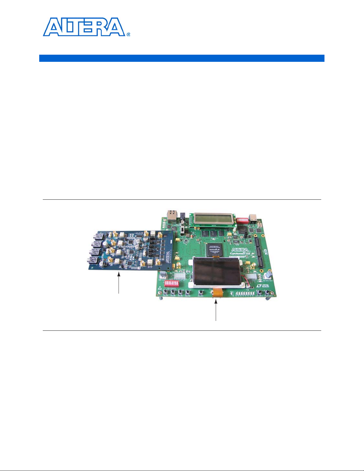
Figure 1–1 shows the Data Conversion HSMC connected to the Cyclone
development board.
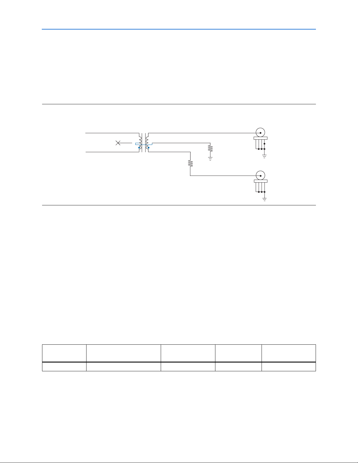
Figure 1–1. Data Conversion HSMC Connected to the Cyclone III FPGA Development Board
f For more information, refer to the DSP Development Kit Getting Started User Guide.
®
III FPGA
© November 2008 Altera Corporation Data Conversion HSMC Reference Manual
Page 6
1–2 Chapter 1: Overview
A/D Channel A
External Clock Input
14-Bit - 150 MS/s
A/D Converter
SMA
SI
CKT
XT_CLK
XT_CLK
SI
CKT
A/D Channel B
SI
CKT
CLK
SEL
14-Bit - 150 MS/s
A/D Converter
SI
CKT
DATA
CNTL
ADA_DCO
ADB_DCO
160 Pin
HSMC
Connector
CLK_A
CLK_B
XT_CLK
14-Bit - 250 MS/s
D/A Converter
SI
CKT
SI
CKT
CLK_A
CLK_B
CLK_A
CLK_B
ADA_DCO
ADB_DCO
SI
CKT
SI
CKT
D/A Channel A
D/A Channel B
14-Bit - 250 MS/s
D/A Converter
SI
CKT
DATA
DATA
DATA
CNTL
Stereo Audio
CODEC
Line in
Mic in
Line out
Headphone
SI
CKT
Note: SI Circuit consists of
a BALUN and Terminators
SMA
SMA
SMA
1/8
"
Phone
Jack
1/8
"
Phone
Jack
1/8
"
Phone
Jack
1/8
"
Phone
Jack
SMA
SMA
CLK_A
CLK_B
XT_CLK
CLK_A
CLK_B
XT_CLK
CLK_A
CLK_B
XT_CLK
External Clock Output
DATA
CNTL
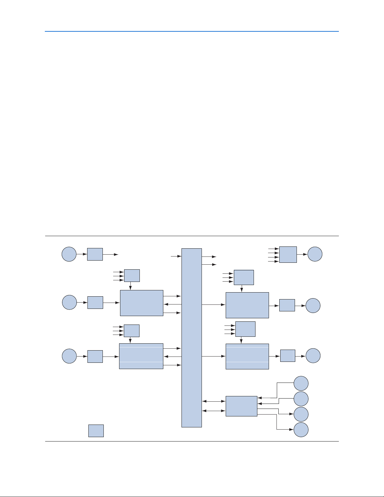
Components and Block Diagram
Components and Block Diagram
Components
The Data Conversion HSMC contains the following components:
■ Interfaces
■ HSMC interface
■ Audio CODEC interface
■ External Clock In interface
■ External Clock Out interface
■ A/D Converter Channels A and B Input interface
■ D/A Converter Channels A and B Output interface
■ Power Supply
2
■ I
C Serial EEPROM
Block Diagram
Figure 1–2 shows the functional block diagram of the Data Conversion HSMC.
Figure 1–2. Data Conversion HSMC Block Diagram
Data Conversion HSMC Reference Manual © November 2008 Altera Corporation
Page 7
2. Board Components and Interfaces
Board Overview
This chapter provides operational and connectivity details about the Data Conversion
HSMC’s major components and interfaces.
Board schematics, board layout database, and assembly files for the Data Conversion
HSMC are included in the board_design_files subdirectory of the installed kit
directory. For information about powering up the Data Conversion HSMC and
installing the demo software and examples, refer to the user guide provided with
your kit.
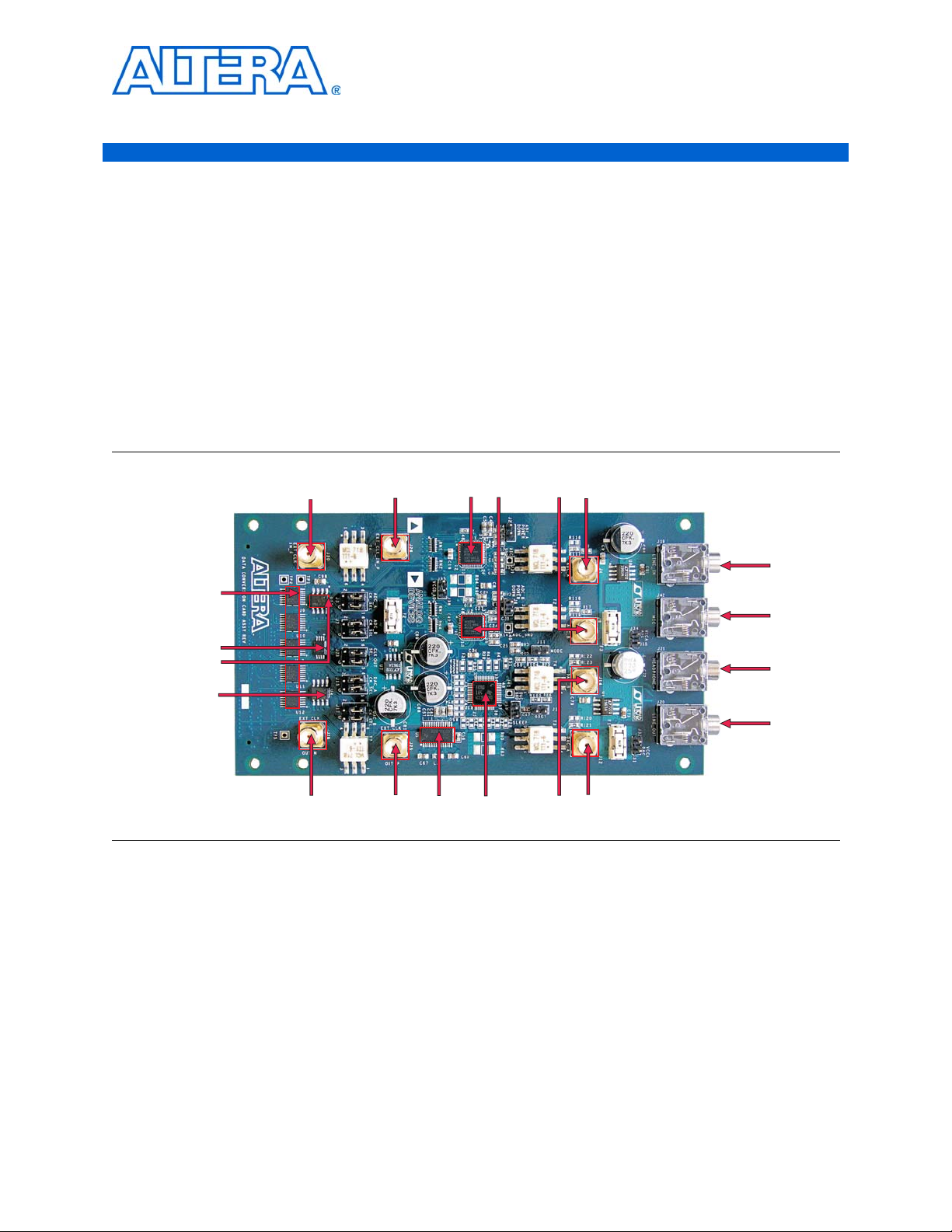
Figure 2–1 shows the layout and components of the Data Conversion HSMC.
Figure 2–1. Data Conversion HSMC Layout and Components
Differential to LVDS
(U9, U10, U11, U12, U13)
Multiplexer
2
IC
Serial
EEPROM (U14)
LVDS Driver
(U15)
LVDS Receiver (U4)
External Clock ln-n
(J30)
External Clock Out-n
(J28)
External Clock ln-p
(J26)
External Clock Out-p
(J25)
Audio
CODEC
Converter
A/D Converter
Channel A (U1)
Channel B (U2)
D/A Converter
Channel A and
Channel B (U3)
A/D Converter Input
Channel A (J4)
Channel B (J8)
D/A Converter Output
Channel A (J12)
Channel B (J14)
Line ln
(J19)
Mic Connecter
(J42)
Headphone
(J21)
Line Out
(J20)
© November 2008 Altera Corporation Data Conversion HSMC Reference Manual
Page 8
2–2 Chapter 2: Board Components and Interfaces
Board Overview
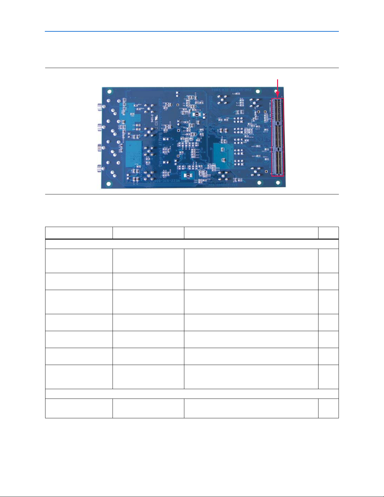
Figure 2–2 shows the back view of the Data Conversion HSMC.
Figure 2–2. Data Conversion HSMC—Back View
HSMC Connector (J1)
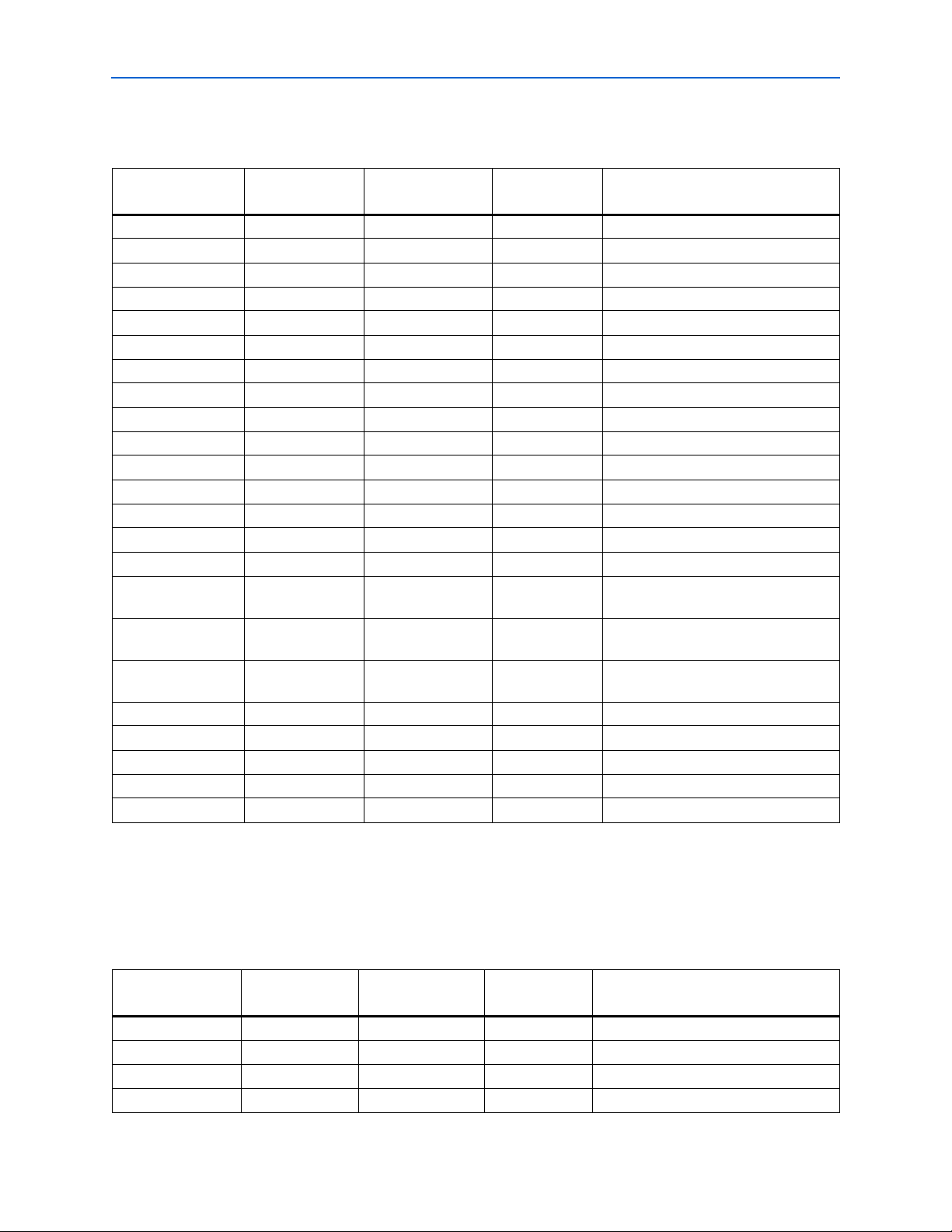
Tab le 2– 1 lists the components and their corresponding board references.
Table 2–1. Data Conversion HSMC Feature Overview (Part 1 of 2)
Board Reference Name Description Page
Configuration, Status, and Setup Elements
J3 (Channel A)
J7 (Channel B)
A/D converter clock select
jumper
Controls which of the three input clock signals
(FPGA clock A, B, or the external SMA clock) is routed
to the A/D converter.
J2 (Channel A)
J6 (Channel B)
J15 (Channel A)
J17 (Channel B)
Power down select jumper Controls whether the A/D converter operates in
power down or power up state.
D/A converter clock select
jumper
Controls which of the three input clock signals
(FPGA clock A, B, or the external SMA clock) is routed
to the D/A converter.
J11 Mode select jumper Controls whether the D/A converter operates in dual
bus mode or interleaved mode.
J10 Gain setting select jumper Controls whether the D/A converter channel’s gain is
set through one or two resistors.
J13 Sleep select jumper Controls whether the D/A converter operates in
power down or power up state.
J23 External clock output select
jumper
Selects which of the four input clocks (FPGA clock A, B
or A/D converter Data Clock Output) is routed to the
SMA clock out (J28).
Clock
J26 (External Clock In-p)
J30 (External Clock In-n)
External clock input SMA
connectors
SMA connectors for a differential clock input. 2–6
2–3
2–4
2–4
2–5
2–5
2–5
2–6
Data Conversion HSMC Reference Manual © November 2008 Altera Corporation
Page 9
Chapter 2: Board Components and Interfaces 2–3
Configuration, Status, and Setup Elements
Table 2–1. Data Conversion HSMC Feature Overview (Part 2 of 2)
Board Reference Name Description Page
J25 (External Clock Out-p)
J28 (External Clock Out-n)
Components and Interfaces
U1 (Channel A)
U2 (Channel B)
J4 (Channel A)
J8 (Channel B)
U3 (Channels A and B) D/A converter Texas Instruments DAC5672. 14-bit, 175 MS/s
J12 (Channel A)
J14 (Channel B)
U5 Audio CODEC Texas Instruments TLV320AK23. Stereo Audio CODEC,
J19 Line-in audio jack 3.5-mm audio connector for line-in 2–15
J20 Line-out audio jack 3.5-mm audio connector for line-out 2–15
J21 Headphone jack 3.5-mm audio connector for headphone 2–15
J42 Mic jack 3.5-mm audio connector for microphone 2–15
J1 HSMC Expansion connector used to interface with Altera
U14 I
External clock output SMA
connectors
A/D converter Analog Devices AD9254. 14-bit, 150 MS/s ADC 2–7
A/D converter input SMAs SMAs that drive the A/D converter inputs 2–11
D/A converter output SMAs SMA outputs for the D/A converters 2–14
2
C EEPROM ISSI EEPROM IS24C02B, 2 Kbits 2–16
SMA connectors for a differential clock output 2–7
2–11
D/A converter
2–14
96 KHz, with integrated headphone amplifier
2–15
development boards
Configuration, Status, and Setup Elements
This section describes configuration, status, and setup elements.
A/D Converter Clock Select Jumper (J3, J7)
Tab le 2– 2 lists the J3 (channel A) and J7 (channel B) jumper settings used to select the
A/D converter clock.
Table 2–2. A/D Converter Clock Select Jumper (J3, J7) Settings (Part 1 of 2)
Schematic Signal Name
Clock Source Board Reference
FPGA Clock HSMC Connector FPGA_CLK_A_P
FPGA Clock HSMC Connector FPGA_CLK_B_P
External Clock External Clock Input SMA XT_IN_P
(1), (2), (3)
FPGA_CLK_A_N
FPGA_CLK_B_N
XT_IN_N
A/D Converter Clock Select (J3 or J7)
Jumper Setting
Pins 3 and 5
Pins 4 and 6
Pins 1 and 3
Pins 4 and 6
Pins 3 and 5
Pins 2 and 4
© November 2008 Altera Corporation Data Conversion HSMC Reference Manual
Page 10
2–4 Chapter 2: Board Components and Interfaces
Configuration, Status, and Setup Elements
Table 2–2. A/D Converter Clock Select Jumper (J3, J7) Settings (Part 2 of 2)
Schematic Signal Name
Clock Source Board Reference
(1), (2), (3)
No Clock — NO_CLK_P
NO_CLK_N
Notes to Table 2–2:
(1) Refer to the appendices for FPGA pin numbers for specific development boards.
(2) On the schematic, MUX (U9) output signal names are ADA_CLK_SEL_P and ADA_CLK_SEL_N.
(3) On the schematic, MUX (U10) output signal names are ADB_CLK_SEL_P and ADB_CLK_SEL_N.
A/D Converter Clock Select (J3 or J7)
Jumper Setting
Pins 1 and 3
Pins 2 and 4
Power Down Select Jumper (J2, J6)
The power down configuration of the A/D converter is selectable through J2 (channel
A) or J6 (channel B). Table 2–3 lists the jumper settings for power down options. A/D
converters should be powered down when not used to reduce spurious noise output.
Table 2–3. Power Down Select Jumper Settings for AD9254 A/D Converter (U1, U2)
A/D Converter Jumper Settings (1) Description
U1 (Channel A) J2 Jumper OFF A/D converter channel A in normal (operational) state
U1 (Channel A) J2 Jumper ON A/D converter channel A in power down
U2 (Channel B) J6 Jumper OFF A/D converter channel B in normal (operational) state
U2 (Channel B) J6 Jumper ON A/D converter channel B in power down
Note to Table 2–3:
(1) If jumper pins are left open, A/D converter will be in normal state.
D/A Converter Clock Select Jumper (J15, J17)
Tab le 2– 4 lists the J15 (channel A) and J17 (channel B) jumper settings used to select
the D/A converter clock.
Table 2–4. D/A Converter Clock Select Jumper (J15, J17) Settings
Schematic Signal Name
Clock Source Board Reference
FPGA Clock HSMC Connector FPGA_CLK_A_P
FPGA_CLK_A_N
FPGA Clock HSMC Connector FPGA_CLK_B_P
FPGA_CLK_B_N
External Clock External Clock Input SMA XT_IN_P
XT_IN_N
No Clock — NO_CLK_P
NO_CLK_N
Notes to Table 2–4:
(1) On the schematic, MUX (U11) output signal names are DAC_CLK_1_P and DAC_CLK_1_N.
(2) On the schematic, MUX (U12) output signal names are DAC_CLK_2_P and DAC_CLK_2_N.
(1) , (2)
D/A Converter Clock Select (J15
or J17) Jumper Setting
Pins 3 and 5
Pins 4 and 6
Pins 1 and 3
Pins 4 and 6
Pins 3 and 5
Pins 2 and 4
Pins 1 and 3
Pins 2 and 4
Data Conversion HSMC Reference Manual © November 2008 Altera Corporation
Page 11
Chapter 2: Board Components and Interfaces 2–5
Configuration, Status, and Setup Elements
Mode Select Jumper (J11)
The mode select jumper is used to put the D/A converter in either dual bus or
interleaved mode. It is selectable through J11 (channel A and channel B). Tab le 2– 5
lists the jumper settings for mode select options.
Table 2–5. Mode Select Jumper (J11) Settings for DAC5672 D/A Converter
Jumper Settings (J11) Description
Jumper ON Interleaved mode
Jumper OFF Dual bus mode
Gain Select Jumper (J10)
The gain setting select jumper is used to set gain of the D/A converter’s channels. It is
selectable through J10 (channel A and channel B). Table 2–6 lists the jumper settings
for gain settings options.
Table 2–6. Gain Select Jumper (J10) Settings for DAC5672 D/A Converter
Jumper Settings
(J10) Description
Jumper ON Sets gain of channel A through RSET on BiasJ_A pin, and of channel B
through RSET on BiasJ_B pin.
Jumper OFF Gain of channels A and B is set through RSET on BiasJ_A pin only and
RSET on BiasJ_B pin is ignored.
Sleep Select Jumper (J13)
The sleep select jumper is used to put the D/A converter in power down mode. It is
selectable through J13 (channel A and channel B). Table 2–7 lists the jumper settings
for sleep select options. The D/A converter when not in use should be put in sleep
mode.
Table 2–7. Sleep Select Jumper (J13) Settings for DAC5672 D/A Converter
Jumper Settings
(J13) Description
Jumper ON Puts D/A converter in power down mode
Jumper OFF D/A converter in normal state
© November 2008 Altera Corporation Data Conversion HSMC Reference Manual
Page 12
2–6 Chapter 2: Board Components and Interfaces
External Clock In
J26 LTI-SASF54GT
XT_CK_IN_N
J30
54
3
2
XT_CK_IN_P
1
54
3
2
R75
1
Unipolar
XT_CK_IN_UNI
R111
0
R112
Bipolar
0
XT_CK_IN_BI
4
5
6
T6
3
2
1
TT1_8_KK91
PS
VTT_XCK
XT_IN_P
1.00K, 1%
XT_IN_N
1.00K, 1%
3.3 V
R78
C70
0.1µF
LTI-SASF54GT
Clocks
External Clock Output Select Jumper (J23)
Tab le 2– 8 lists the external clock output select jumper (J23) settings.
Table 2–8. External Clock Output Select Jumper (J23) Settings
Schematic Signal Name
Clock Source Board Reference
(1)
FPGA Clock HSMC Connector FPGA_CLK_A_P
FPGA_CLK_A_N
FPGA Clock HSMC Connector FPGA_CLK_B_P
FPGA_CLK_B_N
A/D A DCO A/D Channel A ADA_DCO_P
ADA_DCO_N
A/D B DCO A/D Channel B ADB_DCO_P
ADB_DCO_N
Note to Table 2–8:
(1) On the schematic, MUX (U13) output signal names are RX_CLK_P and RX_CLK_N.
Clocks
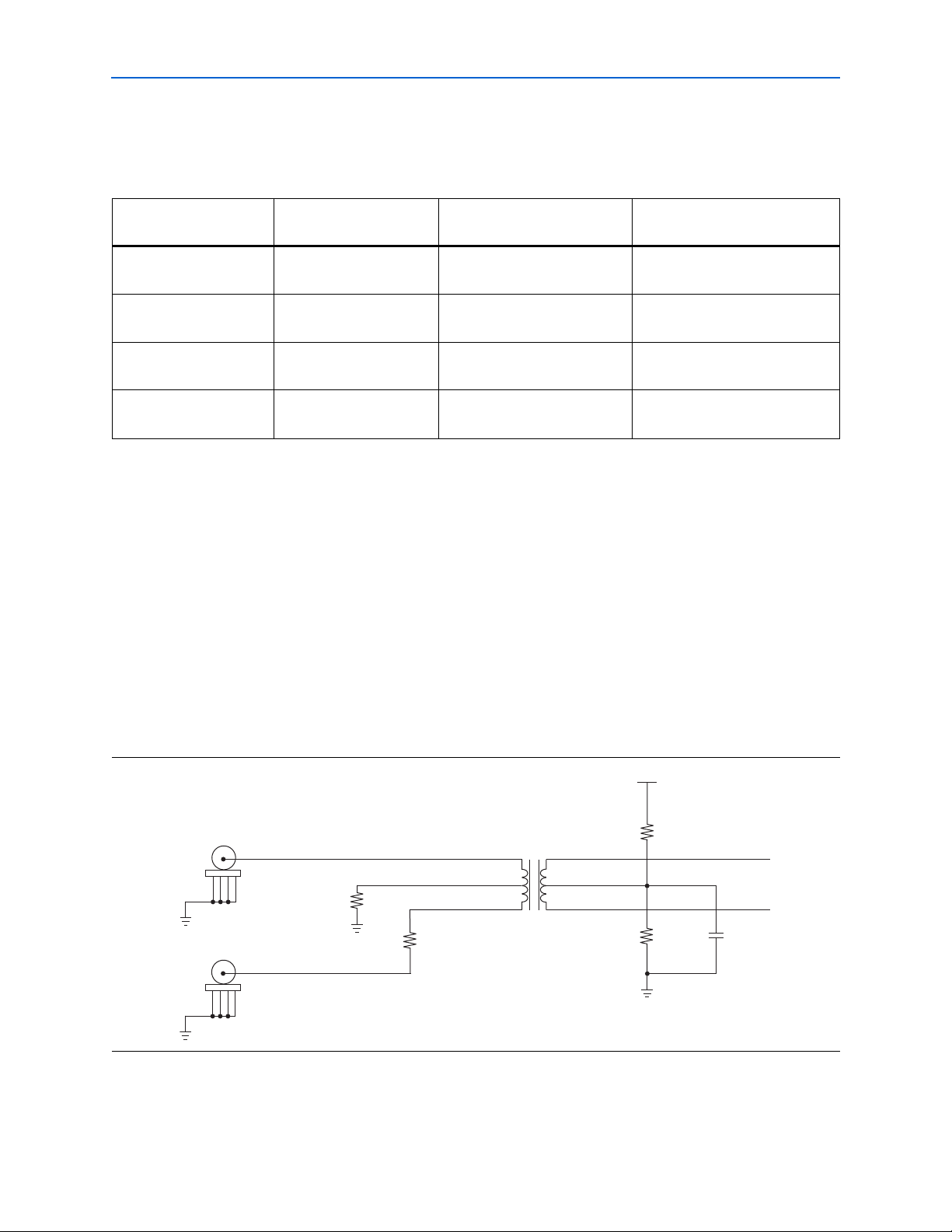
This section describes the external clock input and output SMA connectors.
External Clock Input SMA Connectors (J26, J30)
The CLK SMA connector (J26 or J30) provides an external clock input. It can be
selected to be the input to U1, U2, and U3 (Figure 2–3). An external clock input
provides (while using a particular design) the flexibility to use the same external clock
source for the entire system under test. If you choose to use a single-ended clock, R112
must be removed and R111 be installed.
External Clock Output Select
Jumper (J23) Settings
Pins 3 and 5
Pins 4 and 6
Pins 1 and 3
Pins 4 and 6
Pins 3 and 5
Pins 2 and 4
Pins 1 and 3
Pins 2 and 4
Figure 2–3. External Clock Input Schematic
Data Conversion HSMC Reference Manual © November 2008 Altera Corporation
Page 13
Chapter 2: Board Components and Interfaces 2–7
Component Interfaces
External Clock Output SMA Connectors (J25, J28)
The CLK SMA connector (J25 or J28) provides an external clock output. Different
clocks can be selected by using differential LVDS multiplexer (U13) and clock select
jumper (J23) (Figure 2–4). The external clock source provides (while using a particular
design) the flexibility to alter the input frequency to verify f
choose to use a single-ended clock, R110 must be removed and R109 be installed.
Figure 2–4. External Clock Output Schematic
External Clock Out
tolerances. If you
MAX
RX_CLK_P
RX_CLK_N
Component Interfaces
This section describes the user interfaces, which consist of the A/D converter, D/A
converter, audio CODEC converter, HSMC connector, and I
A/D Converter (U1, U2)
The Data Conversion HSMC contains two AD9254 14-bit 150 MS/s A/D converters.
This device is designed for high-speed and high-performance applications.
The inputs to these A/D converters are transformer-coupled in order to create a
balanced input. The signal-to-noise ratio for the system is up to 72 dB for input signals
from 1 MHz to the Nyquist frequency of the converter. The maximum differential
input voltage to the converter is 2 VPP. Usable voltage input to the SMA connector is
approximately 512 mV when driven from a 50-Ω source.
4
5
NC
6
ADT1_1WT
T7
1
PS
XT_CK_OUT_UNI
2
XT_CK_OUT_BI
3
Bipolar
R110
0
XT_CK_OUT_P
R109
Unipolar
0
LTI-SASF54GT
XT_CK_OUT_N
2
J25LTI-SASF54GT
1
5432
J28
1
5432
C Serial EEPROM.
Tab le 2– 9 lists the A/D converter board reference and manufacturing information.
Table 2–9. A/D Converter Component Reference
Board Reference Device Description Manufacturer
Manufacturing
Part Number
Manufacturer
Website
U1, U2 14-bit, 150 MS/s A/D converter Analog Device AD9254 www.analog.com
© November 2008 Altera Corporation Data Conversion HSMC Reference Manual
Page 14
2–8 Chapter 2: Board Components and Interfaces
Component Interfaces
Tab le 2– 10 provides the pin-out details of the A/D converter channel A.
Table 2–10. A/D converter Channel A (U1) Pin-Out Information
Device
HSMC Signal HSMC Pin Device Signal
Pin Number Description
ADA_D0 79 D0 45 Data Output Bit 0
ADA_D1 77 D1 46 Data Output Bit1
ADA_D2 73 D2 1 Data Output Bit 2
ADA_D3 71 D3 2 Data Output Bit 3
ADA_D4 67 D4 3 Data Output Bit 4
ADA_D5 65 D5 4 Data Output Bit 5
ADA_D6 61 D6 5 Data Output Bit 6
ADA_D7 59 D7 6 Data Output Bit 7
ADA_D8 55 D8 9 Data Output Bit 8
ADA_D9 53 D9 10 Data Output Bit 9
ADA_D10 49 D10 11 Data Output Bit 10
ADA_D11 47 D11 12 Data Output Bit 11
ADA_D12 43 D12 13 Data Output Bit 12
ADA_D13 41 D13 14 Data Output Bit 13
ADA_OR 83 OR 15 Out-of-Range Indicator
AD_SDIO 91 SDIO/DCS 18 Serial Port Interface (SPI) Data
Input/Output (Serial Port Mode)
AD_SCLK 92 SCLK/DFS 19 Serial Port Interface Clock (Serial Port
Mode)
ADA_SPI_CS 89 CSB 20 Serial Port Interface Chip Select
(Active Low)
ADA_OE 85 OEB 43 Output Enable (Active Low)
ADA_DCO 156 DCO 44 Data Clock Output
——ADA_CLK_P 38 (1) Clock Input
——ADA_CLK_N 39 (2) Clock Input
——ADA_PWDN
Notes to Table 2–10:
(1) This pin is connected to Multiplexer pin U9.15.
(2) This pin is connected to Multiplexer pin U9.14.
(3) This pin is connected to Jumper pin J2.2.
36 (3) Power-Down Function Select
Tab le 2– 11 provides the pin-out details of the A/D converter channel B.
Table 2–11. A/D Converter Channel B (U2) Pin-Out Information (Part 1 of 2)
Device
HSMC Signal HSMC Pin Device Signal
Pin Number Description
ADB_D0 80 D0 45 Data Output Bit 0
ADB_D1 78 D1 46 Data Output Bit1
ADB_D2 74 D2 1 Data Output Bit 2
ADB_D3 72 D3 2 Data Output Bit 3
Data Conversion HSMC Reference Manual © November 2008 Altera Corporation
Page 15

Chapter 2: Board Components and Interfaces 2–9
Component Interfaces
Table 2–11. A/D Converter Channel B (U2) Pin-Out Information (Part 2 of 2)
Device
HSMC Signal HSMC Pin Device Signal
Pin Number Description
ADB_D4 68 D4 3 Data Output Bit 4
ADB_D5 66 D5 4 Data Output Bit 5
ADB_D6 62 D6 5 Data Output Bit 6
ADB_D7 60 D7 6 Data Output Bit 7
ADB_D8 56 D8 9 Data Output Bit 8
ADB_D9 54 D9 10 Data Output Bit 9
ADB_D10 50 D10 11 Data Output Bit 10
ADB_D11 48 D11 12 Data Output Bit 11
ADB_D12 44 D12 13 Data Output Bit 12
ADB_D13 42 D13 14 Data Output Bit 13
ADB_OR 84 OR 15 Out-of-Range Indicator
AD_SDIO 91 SDIO/DCS 18 Serial Port Interface (SPI) Data
Input/Output (Serial Port Mode)
AD_SCLK 92 SCLK/DFS 19 Serial Port Interface Clock (Serial Port
Mode)
ADB_SPI_CS 90 CSB 20 Serial Port Interface Chip Select
(Active Low)
ADB_OE 86 OEB 43 Output Enable (Active Low)
ADB_DCO 158 DCO 44 Data Clock Output
——ADB_CLK_P 38 (1) Clock Input
——ADB_CLK_N 39 (2) Clock Input
——ADB_PWDN 36 (3) Power-Down Function Select
Notes to Table 2–11:
(1) This pin is connected to Multiplexer pin U10.15.
(2) This pin is connected to Multiplexer pin U10.14.
(3) This pin is connected to Jumper pin J6.2.
A/D Converter Clocks
Figure 2–5 shows the components involved in selecting the clock signal to be sent to
the AD9254 A/D converter (U1 for channel A, U2 for channel B). J3 (channel A) or J7
(channel B) selects the A/D clock from the FPGA clock A, the FPGA clock B, or the
external SMA clock (J26 and J30). The selected A/D clock passes through a differential
to LVDS clock multiplexer (U9 for channel A, U10 for channel B), which provides the
clock signal to the AD9254.
© November 2008 Altera Corporation Data Conversion HSMC Reference Manual
Page 16

2–10 Chapter 2: Board Components and Interfaces
ADA_OE
ADA_CLK_P
ADA_CLK_N
ADA_OE
ADA_CLK_N
ADA_CLK_P
ADA_SPI_CS
ADA_SDIO
ADA_ACLK
FPGA_CLK_A_P
NO_CLK_P
NO_CLK_N
ADA_CLK_S1
ADA_CLK_S0
PCLK0P
PCLK0N
PCLK1P
PCLK1N
PCLK2P
PCLK2N
PCLK3P
PCLK3N
SEL0
SEL1
VDD
VDD
QP
QN
GND
GND
3.3 V
ADA_CLK_SEL_N
ADA_CLK_SEL_P
ADA_SPI_CS
ADA_SDIO
ADA_SCLK
FPGA_CLK_A_N
FPGA_CLK_A_P
FPGA_CLK_A_N12
3
4
FPGA_CLK_B_P
FPGA_CLK_B_N
FPGA_CLK_B_P
FPGA_CLK_B_N
XT_IN_P
XT_IN_N
XT_IN_P
XT_IN_N
9
10
11
12
NO_CLK_P
NO_CLK_N
6
7
13
8
15
14
5
16
C98
C99
C100
10µF 0.1µF 1.0nF
ICS854054
U9
ADB_OE
ADB_CLK_P
ADB_CLK_N
ADB_OE
ADB_CLK_N
ADB_CLK_P
ADB_SPI_CS
AD_SDIO
AD_SCLK
FPGA_CLK_A_P
NO_CLK_P
NO_CLK_N
ADB_CLK_S1
ADB_CLK_S0
PCLK0P
PCLK0N
PCLK1P
PCLK1N
PCLK2P
PCLK2N
PCLK3P
PCLK3N
SEL0
SEL1
VDD
VDD
QP
QN
GND
GND
3.3 V
ADB_CLK_SEL_N
ADB_CLK_SEL_P
ADB_SPI_CS
AD_SDIO
AD_SCLK
FPGA_CLK_A_N
FPGA_CLK_A_P
FPGA_CLK_A_N12
3
4
FPGA_CLK_B_P
FPGA_CLK_B_N
FPGA_CLK_B_P
FPGA_CLK_B_N
XT_IN_P
XT_IN_N
XT_IN_P
XT_IN_N
9
10
11
12
NO_CLK_P
NO_CLK_N
6
7
13
8
15
14
5
16
C101 C102
1.0nF0.1µF
ICS854054
U10
Component Interfaces
Figure 2–5. A/D Converter Clocking Options
Table 2–12. Differential to LVDS Clock Multiplexer (U9, U10) Pin-Out Information (Part 1 of 2)
Schematic Signal
FPGA_CLK_A_P 95 PCLK0P 1 Non-inverting Differential clock input
FPGA_CLK_A_N 97 PCLK0N 2 Inverting Differential clock input
FPGA_CLK_B_P 155 PCLK1P 3 Non-inverting Differential clock input
FPGA_CLK_B_N 157 PCLK1N 4 Inverting Differential clock input
Data Conversion HSMC Reference Manual © November 2008 Altera Corporation
Tab le 2– 12 provides the differential to LVDS clock multiplexer pin-out details.
HSMC
Connector
Pin Number Device Signal
Device Pin
Number Description
Page 17

Chapter 2: Board Components and Interfaces 2–11
Component Interfaces
Table 2–12. Differential to LVDS Clock Multiplexer (U9, U10) Pin-Out Information (Part 2 of 2)
HSMC
Connector
Schematic Signal
XT_IN_P 96 PCLK2P 9 Non-inverting Differential clock input
XT_IN_N 98 PCLK2N 10 Inverting Differential clock input
AD(A,B)_CLK_SEL_P — QP 15 Non-inverting Differential Clock Output
AD(A,B)_CLK_SEL_N — QN 14 Inverting Differential Clock Output
Pin Number Device Signal
Device Pin
Number Description
A/D Converter Input SMA Connector (J4, J8)
J4 (channel A) and J8 (channel B) are standard through-hole SMA connectors used to
interface the AD9254 A/D converter input with SMA cables.
D/A Converter (U3)
The D/A converter (U3 for channels A and B) on the Data Conversion HSMC
provides 14-bit resolution and produces samples at rates up to 275 MS/s. It is a
high-speed TI DAC5672 D/A converter and is set up to drive a differential-to-single
output through a transformer. The output is transformer coupled and can be found on
the SMA connector (J12 for channel A, J14 for channel B). The output of the
TI DAC5672 D/A converter is set to the maximum output current of 20 mA. The
signal-to-noise ratio for the system is up to 60 dB for output signals from 1 MHz to the
Nyquist frequency of the converter.
Tab le 2– 13 lists the D/A converter board reference and manufacturing information.
Table 2–13. D/A Converter Component Reference
Manufacturing
Board Reference Device Description Manufacturer
U3 14-bit, 275 MS/s D/A converter Texas Instruments DAC5672 www.ti.com
Part Number
Manufacturer
Website
Tab le 2– 14 provides the pin-out details of the D/A converter channel A and
channel B.
Table 2–14. D/A Converter Channel A and Channel B (U3) Pin-Out Information (Part 1 of 2)
Device Pin
HSMC Signal HSMC Pin Device Signal
DA0 139 DA0 14 Data port A0
DA1 137 DA1 13 Data port A1
DA2 133 DA2 12 Data port A2
DA3 131 DA3 11 Data port A3
DA4 127 DA4 10 Data port A4
DA5 125 DA5 9 Data port A5
DA6 121 DA6 8 Data port A6
DA7 119 DA7 7 Data port A7
DA8 115 DA8 6 Data port A8
DA9 113 DA9 5 Data port A9
Number Description
© November 2008 Altera Corporation Data Conversion HSMC Reference Manual
Page 18

2–12 Chapter 2: Board Components and Interfaces
Component Interfaces
Table 2–14. D/A Converter Channel A and Channel B (U3) Pin-Out Information (Part 2 of 2)
Device Pin
HSMC Signal HSMC Pin Device Signal
Number Description
DA10 109 DA10 4 Data port A10
DA11 107 DA11 3 Data port A11
DA12 103 DA12 2 Data port A12
DA13 101 DA13 1 Data port A13
DB0 140 DB0 36 Data port B0
DB1 138 DB1 35 Data port B1
DB2 134 DB2 34 Data port B2
DB3 132 DB3 33 Data port B3
DB4 128 DB4 32 Data port B4
DB5 126 DB5 31 Data port B5
DB6 122 DB6 30 Data port B6
DB7 120 DB7 29 Data port B7
DB8 116 DB8 28 Data port B8
DB9 114 DB9 27 Data port B9
DB10 110 DB10 26 Data port B10
DB11 108 DB11 25 Data port B11
DB12 104 DB12 24 Data port B12
DB13 102 DB13 23 Data port B13
——CLKA 18 (1) Clock input for DACA, CLKIQ in
interleaved mode
——CLKB 19 (2) Clock input for DACB, RESETIQ in
——GSET 42 (3) Gain-setting mode: H – 1 resistor,
——MODE 48 (4) Mode Select: H – Dual Bus,
——SLEEP 37 (5)
Notes to Table 2–14:
(1) This pin is connected to Differential Receiver pin U4.7.
(2) This pin is connected to Differential Receiver pin U4.6.
(3) This pin is connected to Jumper pin J10.1.
(4) This pin is connected to Jumper pin J11.1.
(5) This pin is connected to Jumper pin J13.2.
interleaved mode
L – 2 resistors. Internal pull-up.
L – Interleaved. Internal pull-up.
Sleep function control input: H – DAC in
power-down mode, L – DAC in operating
mode. Internal pull-down.
Data Conversion HSMC Reference Manual © November 2008 Altera Corporation
Page 19

Chapter 2: Board Components and Interfaces 2–13
FPGA_CLK_A_P
NO_CLK_P
NO_CLK_N
DAA_CLK_S1
DAA_CLK_S0
PCLK0P
PCLK0N
PCLK1P
PCLK1N
PCLK2P
PCLK2N
PCLK3P
PCLK3N
SEL0
SEL1
VDD
VDD
QP
QN
GND
GND
3.3 V
DAC_CLK_1_N
DAC_CLK_1_P
FPGA_CLK_A_N
FPGA_CLK_A_P
FPGA_CLK_A_N12
3
4
FPGA_CLK_B_P
FPGA_CLK_B_N
FPGA_CLK_B_P
FPGA_CLK_B_N
XT_IN_P
XT_IN_N
XT_IN_P
XT_IN_N
9
10
11
12
NO_CLK_P
NO_CLK_N
6
7
13
8
15
14
5
16
C103
C104
0.1µF
1.0nF
ICS854054
U11
FPGA_CLK_A_P
NO_CLK_P
NO_CLK_N
DAB_CLK_S1
DAB_CLK_S0
PCLK0P
PCLK0N
PCLK1P
PCLK1N
PCLK2P
PCLK2N
PCLK3P
PCLK3N
SEL0
SEL1
VDD
VDD
QP
QN
GND
GND
3.3 V
DAC_CLK_2_N
DAC_CLK_2_P
FPGA_CLK_A_N
FPGA_CLK_A_P
FPGA_CLK_A_N12
3
4
FPGA_CLK_B_P
FPGA_CLK_B_N
FPGA_CLK_B_P
FPGA_CLK_B_N
XT_IN_P
XT_IN_N
XT_IN_P
XT_IN_N
9
10
11
12
NO_CLK_P
NO_CLK_N
6
7
13
8
15
14
5
16
C105 C106
1.0nF0.1µF
ICS854054
U12
Component Interfaces
D/A Converter Clocks
Figure 2–6 shows the components involved in selecting the clock signal to be sent to
the DAC5672 (U3 for channels A and B). J15 (channel A) or J17 (channel B) selects the
D/A clock from the FPGA clock A, the FPGA clock B, or the SMA clock (J26 and J30).
The selected D/A clock passes through a differential to LVDS clock multiplexer (U11
for channel A, U12 for channel B), which provides the clock signal to 2-bit high-speed
differential receiver FIN1028, which in turn outputs clock to the DAC5672 (refer to
“D/A Converter Clock Select Jumper (J15, J17)” on page 2–4.)
Figure 2–6. D/A Converter Clocking Options
© November 2008 Altera Corporation Data Conversion HSMC Reference Manual
Page 20

2–14 Chapter 2: Board Components and Interfaces
Component Interfaces
Tab le 2– 15 provides the differential to LVDS clock multiplexer pin-out details.
Table 2–15. Differential to LVDS Clock Multiplexer (U11, U12) Pin-Out Information
HSMC
Connector
Schematic Signal
FPGA_CLK_A_P 95 PCLK0P 1 Non-inverting Differential clock input
FPGA_CLK_A_N 97 PCLK0N 2 Inverting Differential clock input
FPGA_CLK_B_P 155 PCLK1P 3 Non-inverting Differential clock input
FPGA_CLK_B_N 157 PCLK1N 4 Inverting Differential clock input
XT_IN_P 96 PCLK2P 9 Non-inverting Differential clock input
XT_IN_N 98 PCLK2N 10 Inverting Differential clock input
DA(A,B)_CLK_SEL_P — QP 15 Non-inverting Differential Clock Output
DA(A,B)_CLK_SEL_N — QN 14 Inverting Differential Clock Output
Pin Number Device Signal
Device
Pin Number Description
D/A Converter Output SMA Connector (J12, J14)
J12 (channel A) and J14 (channel B) are standard through-hole SMA connectors used
to interface the DAC5672 D/A converter output with SMA cables.
Audio CODEC Converter (U5)
The Data Conversion HSMC contains three stereo jack and one mic jack connectors
which provide one stereo output, one stereo input, one amplified stereo headphone
output, and one microphone input. The stereo jacks are driven by a stereo audio
CODEC running at 8 to 96 kHz. Tab le 2– 16 lists the audio CODEC board reference
and manufacturing information.
Table 2–16. Audio CODEC Converter Component Reference
Manufacturing
Board Reference Description Manufacturer
U5 Stereo Audio CODEC, 8–96 KHz, with
Integrated Headphone Amplifier
Texas Instruments TLV320AIC23 www.ti.com
Part Number
Tab le 2– 17 provides the TI TLV320AIC23 audio CODEC pin-out details.
Table 2–17. Audio CODEC Converter (U5) Pin-Out Information (Part 1 of 2)
Device
HSMC Signal HSMC Pin Device Signal
AIC_XCLK 150 XTI/MCLK 25 Crystal or external-clock input. Used for derivation of all
AIC_LRCOUT 146 LRCOUT 7 I2S A/D converter-word clock signal. In audio master
AIC_LRCIN 145 LRCIN 5 I2S D/A converter-word clock signal. In audio master
Pin Number Description
internal clocks on the AIC23B.
mode, the AIC23B generates this framing signal and sends
it to the DSP. In audio slave mode, the signal is generated
by the DSP.
mode, the AIC23B generates this framing signal and sends
it to the DSP. In audio slave mode, the signal is generated
by the DSP.
Manufacturer
Website
Data Conversion HSMC Reference Manual © November 2008 Altera Corporation
Page 21

Chapter 2: Board Components and Interfaces 2–15
Component Interfaces
Table 2–17. Audio CODEC Converter (U5) Pin-Out Information (Part 2 of 2)
Device
HSMC Signal HSMC Pin Device Signal
Pin Number Description
AIC_DIN 143 DIN 4 I2S format serial data input to the sigma-delta stereo
D/A converter.
AIC_DOUT 144 DOUT 6 I2S format serial data output from the sigma-delta stereo
A/D converter.
AD_SCLK 92 SCLK 24 Control-port serial-data clock. For serial peripheral
interface (SPI) and 2-wire control modes, this is the
serial-clock input.
AD_SDIO 91 SDIN 23 I2S format serial data input to the sigma-delta stereo
D/A converter.
AIC_SPI_CS 151 CS_n 21 Serial Control Interface Chip Select (Active Low).
AIC_BCLK 149 BCLK 3 I2S serial-bit clock. In audio master mode, the AIC23B
generates this signal and sends it to the DSP. In audio slave
mode, the signal is generated by the DSP.
Audio Jacks (J19, J20, J21, J42)
The Data Conversion HSMC contains the following audio connectors:
■ J19—an audio connector for line-in
■ J20—an audio connector for line-out
■ J21—an audio connector for amplified line-out
■ J42—an audio connector for microphone
HSMC Connector (J1)
The Data Conversion HSMC connects to Altera FPGA starter and development
boards through a single HSMC connector (J6).
Tab le 2– 18 lists the HSMC connector board reference and manufacturing information.
Table 2–18. Audio CODEC Converter Component Reference
Manufacturing
Board Reference Description Manufacturer
Part Number
J1 High-Speed Mezzanine Card Connector Samtec ASP-122952-01 www.samtec.com
The HSMC connector is a modified version of the standard high-speed Samtec
connectors. To provide better integrity between host boards and daughter cards when
using high-speed transceivers, the standard high-speed Samtec connector is modified
by removing every third pin in bank 1.
Manufacturer
Website
1 CMOS utilization of the HSMC pins is assumed and no options for supporting other
differential signaling are provided with the board. The eight clock-data-recovery
high-speed transceiver channels are not connected on this HSMC.
© November 2008 Altera Corporation Data Conversion HSMC Reference Manual
Page 22

2–16 Chapter 2: Board Components and Interfaces
2.413
((90 POS / 30 x .7875) + .050)
.78 REF
.626 REF
.036 REF
.006 REF
.245 REF
.150 REF
01
02
.285 REF
DP Bank
.571
(29 EQ Spaces @ .0197)
Component Interfaces
Figure 2–7 shows the HSMC connector layout.
Figure 2–7. Samtec Header Connector
I2C Serial EEPROM (U14)
There is a 2-Kbit I2C Serial EEPROM on the Data Conversion HSMC. Table 2–19 lists
2
the I
C Serial EEPROM board reference and manufacturing information.
Table 2–19. I2C Serial EEPROM Component Reference
Manufacturing
Board Reference Description Manufacturer
2
U14 2-Kbit I
C Serial EEPROM ISSI IS24C02B www.issi.com
Tab le 2– 20 provides the pin-out details of the I
2
Part Number
C Serial EEPROM with HSMC
connector.
Table 2–20. I2C Serial EEPROM (U14) Pin-Out Information
Device
HSMC Signal HSMC Pin Device Signal
Pin Number Description
SCL 34 SCL 6 Serial Clock Input
SDA 33 SDA 5 Serial Address/Data I/O
Manufacturer
Website
Data Conversion HSMC Reference Manual © November 2008 Altera Corporation
Page 23

Chapter 2: Board Components and Interfaces 2–17
3.3 V
R95
R99
R100
NL-1.00K, 1%
NL-1.00K, 1%
NL-1.00K, 1%
R101
R102
R103
1.00K, 1%
1.00K, 1%
1.00K, 1%
U14
VCC
SCL
A0
A1
A2
SDA
WP
GND
3.3 V
8
1
2
3
IS24C02B
7
4
5
6
SCL
SDA
Power Supply
Figure 2–8 shows the I2C Serial EEPROM schematic.
Figure 2–8. I2C Serial EEPROM Schematic
Power Supply
A/D Power Supplies (U6, U7, U8)
The power supply block distributes clean power from the 12-V and 3.3-V input
supply (from the host board through the HSMC connector) to the Data Conversion
HSMC through on-board regulators. To provide various voltage options, the board
uses several Linear Technologies regulators.
Tab le 2– 21 lists the Power Supplies board reference and manufacturing information.
Table 2–21. Power Supplies Component Reference
Board Reference Description Manufacturer
U6, U7, U8 LT1963A - 1.5A, Low Noise, Fast
Transient Response LDO Regulators
Linear
Technologies
Manufacturing
Part Number
Manufacturer
Website
LT1963 www.linear.com
© November 2008 Altera Corporation Data Conversion HSMC Reference Manual
Page 24

2–18 Chapter 2: Board Components and Interfaces
Power Supply
Data Conversion HSMC Reference Manual © November 2008 Altera Corporation
Page 25

A. Pin-Out Information for the Cyclone III
(3C120) Development Board
Tab le A– 1 provides the HSMC Port A interface pin-out information for the Cyclone III
EP3C120F780 development board.
Table A–1. HSMC Port A Interface Pin-Out Information (Part 1 of 4)
Data Conversion HSMC Schematic Development Board Schematic
Cyclone
Board
Reference
(J1) Description
33 Management serial data SDA HSMA_SDA 2.5 V AC1
34 Management serial clock SCL HSMA_SCL 2.5 V AC3
41 Dedicated CMOS I/O bit 0 ADA_D13 HSMA_D0 2.5 V AB6
42 Dedicated CMOS I/O bit 1 ADB_D13 HSMA_D1 2.5 V AF2
43 Dedicated CMOS I/O bit 2 ADA_D12 HSMA_D2 2.5 V AE3
44 Dedicated CMOS I/O bit 3 ADB_D12 HSMA_D3 2.5 V AC5
47 LVDS TX or CMOS I/O bit 0 ADA_D11 HSMA_TX_D_P0 LVDS or
48 LVDS RX or CMOS I/O bit 0 ADB_D11 HSMA_RX_D_P0 LVDS or
49 LVDS TX or CMOS I/O bit 0 ADA_D10 HSMA_TX_D_N0 LVDS or
50 LVDS RX or CMOS I/O bit 0 ADB_D10 HSMA_RX_D_N0 LVDS or
53 LVDS TX bit 1p or CMOS I/O data 8 ADA_D9 HSMA_TX_D_P1 LVDS or
54 LVDS RX bit 1p or CMOS I/O data 9 ADB_D9 HSMA_RX_D_P1 LVDS or
55 LVDS TX bit 1n or CMOS I/O data bit 10 ADA_D8 HSMA_TX_D_N1 LVDS or
56 LVDS RX bit 1n or CMOS I/O data bit 11 ADB_D8 HSMA_RX_D_N1 LVDS or
59 LVDS TX bit 2p or CMOS I/O data bit 12 ADA_D7 HSMA_TX_D_P2 LVDS or
60 LVDS RX bit 2p or CMOS I/O data bit 13 ADB_D7 HSMA_RX_D_P2 LVDS or
61 LVDS TX bit 2n or CMOS I/O data bit 14 ADA_D6 HSMA_TX_D_N2 LVDS or
62 LVDS RX bit 2n or CMOS I/O data bit 15 ADB_D6 HSMA_RX_D_N2 LVDS or
65 LVDS TX bit 3p or CMOS I/O data bit 16 ADA_D5 HSMA_TX_D_P3 LVDS or
Schematic
Signal Name
Schematic
Signal Name
I/O
Standard
2.5 V
2.5 V
2.5 V
2.5 V
2.5 V
2.5 V
2.5 V
2.5 V
2.5 V
2.5 V
2.5 V
2.5 V
2.5 V
Number
III
Pin
R7
AB2
R6
AB1
V4
Y4
V3
Y3
T4
U3
T3
U4
R3
© November 2008 Altera Corporation Data Conversion HSMC Reference Manual
Page 26

A–2 Appendix A: Pin-Out Information for the Cyclone III (3C120)
Development Board
Table A–1.
HSMC Port A Interface Pin-Out Information (Part 2 of 4)
Data Conversion HSMC Schematic Development Board Schematic
Board
Reference
(J1) Description
Schematic
Signal Name
Schematic
Signal Name
I/O
Standard
66 LVDS RX bit 3p or CMOS I/O data bit 17 ADB_D5 HSMA_RX_D_P3 LVDS or
2.5 V
67 LVDS TX bit 3n or CMOS I/O data bit 18 ADA_D4 HSMA_TX_D_N3 LVDS or
2.5 V
68 LVDS RX bit 3n or CMOS I/O data bit 19 ADB_D4 HSMA_RX_D_N3 LVDS or
2.5 V
71 LVDS TX bit 4p or CMOS I/O data bit 20 ADA_D3 HSMA_TX_D_P4 LVDS or
2.5 V
72 LVDS RX bit 4p or CMOS I/O data bit 21 ADB_D3 HSMA_RX_D_P4 LVDS or
2.5 V
73 LVDS TX or 4n CMOS I/O data bit 22 ADA_D2 HSMA_TX_D_N4 LVDS or
2.5 V
74 LVDS RX 4n or CMOS I/O data bit 23 ADB_D2 HSMA_RX_D_N4 LVDS or
2.5 V
77 LVDS TX 5p or CMOS I/O data bit 24 ADA_D1 HSMA_TX_D_P5 LVDS or
2.5 V
78 LVDS RX 5p or CMOS I/O data bit 25 ADB_D1 HSMA_RX_D_P5 LVDS or
2.5 V
79 LVDS TX 5n or CMOS I/O data bit 26 ADA_D0 HSMA_TX_D_N5 LVDS or
2.5 V
80 LVDS RX 5n or CMOS I/O data bit 27 ADB_D0 HSMA_RX_D_N5 LVDS or
2.5 V
83 LVDS TX 6p or CMOS I/O data bit 28 ADA_OR HSMA_TX_D_P6 LVDS or
2.5 V
84 LVDS RX 6p or CMOS I/O data bit 29 ADB_OR HSMA_RX_D_P6 LVDS or
2.5 V
85 LVDS TX 6n or CMOS I/O data bit 30 ADA_OE HSMA_TX_D_N6 LVDS or
2.5 V
86 LVDS RX 6n or CMOS I/O data bit 31 ADB_OE HSMA_RX_D_N6 LVDS or
2.5 V
89 LVDS TX 7p or CMOS I/O data bit 32 ADA_SPI_CS HSMA_TX_D_P7 LVDS or
2.5 V
90 LVDS RX 7p or CMOS I/O data bit 33 ADB_SPI_CS HSMA_RX_D_P7 LVDS or
2.5 V
91 LVDS TX 7n or CMOS I/O data bit 34 AD_SDIO HSMA_TX_D_N7 LVDS or
2.5 V
92 LVDS RX 7n or CMOS I/O data bit 35 AD_SCLK HSMA_RX_D_N7 LVDS or
2.5 V
95 LVDS or CMOS clock out FPGA_CLK_A_P HSMA_CLK_OUT_P1 LVDS or
2.5 V
Cyclone
III
Pin
Number
W2
R4
W1
M8
V2
M7
V1
P2
U2
P1
U1
M4
U6
M3
U5
M2
R2
M1
R1
G6
Data Conversion HSMC Reference Manual © November 2008 Altera Corporation
Page 27

Appendix A: Pin-Out Information for the Cyclone III (3C120) Development Board A–3
Table A–1.
HSMC Port A Interface Pin-Out Information (Part 3 of 4)
Data Conversion HSMC Schematic Development Board Schematic
Board
Reference
(J1) Description
Schematic
Signal Name
Schematic
Signal Name
I/O
Standard
96 LVDS or CMOS clock in XT_IN_P HSMA_CLK_IN_P1 LVDS or
2.5 V
97 LVDS or CMOS clock out FPGA_CLK_A_N HSMA_CLK_OUT_N1 LVDS or
2.5 V
98 LVDS or CMOS clock in XT_IN_N HSMA_CLK_IN_N1 LVDS or
2.5 V
101 LVDS TX 8p or CMOS I/O data bit 40 DA13 HSMA_TX_D_P8 LVDS or
2.5 V
102 LVDS RX 8p or CMOS I/O data bit 41 DB13 HSMA_RX_D_P8 LVDS or
2.5 V
103 LVDS TX 8n or CMOS I/O data bit 42 DA12 HSMA_TX_D_N8 LVDS or
2.5 V
104 LVDS RX 8n or CMOS I/O data bit 43 DB12 HSMA_RX_D_N8 LVDS or
2.5 V
107 LVDS TX 9p or CMOS I/O data bit 44 DA11 HSMA_TX_D_P9 LVDS or
2.5 V
108 LVDS RX 9p or CMOS I/O data bit 45 DB11 HSMA_RX_D_P9 LVDS or
2.5 V
109 LVDS TX 9n or CMOS I/O data bit 46 DA10 HSMA_TX_D_N9 LVDS or
2.5 V
110 LVDS RX 9n or CMOS I/O data bit 47 DB10 HSMA_RX_D_N9 LVDS or
2.5 V
113 LVDS TX 10p or CMOS I/O data bit 48 DA9 HSMA_TX_D_P10 LVDS or
2.5 V
114 LVDS RX 10p or CMOS I/O data bit 49 DB9 HSMA_RX_D_P10 LVDS or
2.5 V
115 LVDS TX 10n or CMOS I/O data bit 50 DA8 HSMA_TX_D_N10 LVDS or
2.5 V
116 LVDS RX 10n or CMOS I/O data bit 51 DB8 HSMA_RX_D_N10 LVDS or
2.5 V
119 LVDS TX 11p or CMOS I/O data bit 52 DA7 HSMA_TX_D_P11 LVDS or
2.5 V
120 LVDS RX 11p or CMOS I/O data bit 53 DB7 HSMA_RX_D_P11 LVDS or
2.5 V
121 LVDS TX 11n or CMOS I/O data bit 54 DA6 HSMA_TX_D_N11 LVDS or
2.5 V
122 LVDS RX 11n or CMOS I/O data bit 55 DB6 HSMA_RX_D_N11 LVDS or
2.5 V
125 LVDS TX 12p or CMOS I/O data bit 56 DA5 HSMA_TX_D_P12 LVDS or
2.5 V
Cyclone
III
Pin
Number
Y2
G5
Y1
L7
N4
L6
N3
K8
L4
L8
L3
K4
L2
K3
L1
J4
K2
J3
K1
J7
© November 2008 Altera Corporation Data Conversion HSMC Reference Manual
Page 28

A–4 Appendix A: Pin-Out Information for the Cyclone III (3C120)
Development Board
Table A–1. HSMC Port A Interface Pin-Out Information (Part 4 of 4)
Data Conversion HSMC Schematic Development Board Schematic
Cyclone
Board
Reference
(J1) Description
Schematic
Signal Name
Schematic
Signal Name
I/O
Standard
126 LVDS RX 12p or CMOS I/O data bit 57 DB5 HSMA_RX_D_P12 LVDS or
III
Pin
Number
J6
2.5 V
127 LVDS TX 12n or CMOS I/O data bit 58 DA4 HSMA_TX_D_N12 LVDS or
K7
2.5 V
128 LVDS RX 12n or CMOS I/O data bit 59 DB4 HSMA_RX_D_N12 LVDS or
J5
2.5 V
131 LVDS TX 13p or CMOS I/O data bit 60 DA3 HSMA_TX_D_P13 LVDS or
G2
2.5 V
132 LVDS RX 13p or CMOS I/O data bit 61 DB3 HSMA_RX_D_P13 LVDS or
H4
2.5 V
133 LVDS TX 13n or CMOS I/O data bit 62 DA2 HSMA_TX_D_N13 LVDS or
G1
2.5 V
134 LVDS RX 13n or CMOS I/O data bit 63 DB2 HSMA_RX_D_N13 LVDS or
H3
2.5 V
137 LVDS TX 14p or CMOS I/O data bit 64 DA1 HSMA_TX_D_P14 LVDS or
F5
2.5 V
138 LVDS TX 14p or CMOS I/O data bit 65 DB1 HSMA_RX_D_P14 LVDS or
G4
2.5 V
139 LVDS RX 14n or CMOS I/O data bit 66 DA0 HSMA_TX_D_N14 LVDS or
F4
2.5 V
140 LVDS RX 14n or CMOS I/O data bit 67 DB0 HSMA_RX_D_N14 LVDS or
G3
2.5 V
143 LVDS RX 15p or CMOS I/O data bit 68 AIC_DIN HSMA_TX_D_P15 LVDS or
E2
2.5 V
144 LVDS TX 15p or CMOS I/O data bit 69 AIC_DOUT HSMA_RX_D_P15 LVDS or
F2
2.5 V
145 LVDS RX 15n or CMOS I/O data bit 70 AIC_LRCIN HSMA_TX_D_N15 LVDS or
E1
2.5 V
146 LVDS TX 15n or CMOS I/O data bit 71 AIC_LRCOUT HSMA_RX_D_N15 LVDS or
F1
2.5 V
149 LVDS RX 16p or CMOS I/O data bit 72 AIC_BCLK HSMA_TX_D_P16 LVDS or
D3
2.5 V
150 LVDS TX 16p or CMOS I/O data bit 73 AIC_XCLK HSMA_RX_D_P16 LVDS or
E3
2.5 V
151 LVDS TX 16n or CMOS I/O data bit 74 AIC_SPI_CS HSMA_TX_D_N16 LVDS or
C2
2.5 V
155 LVDS or CMOS clock out FPGA_CLK_B_P HSMA_CLK_OUT_P2 LVDS D2
156 LVDS or CMOS clock in ADA_DCO HSMA_CLK_IN_P2 LV DS J2
157 LVDS or CMOS clock out FPGA_CLK_B_N HSMA_CLK_OUT_N2 2.5 V D1
158 LVDS or CMOS clock in ADB_DCO HSMA_CLK_IN_N2
2.5 V J1
Data Conversion HSMC Reference Manual © November 2008 Altera Corporation
Page 29

Appendix A: Pin-Out Information for the Cyclone III (3C120) Development Board A–5
Tab le A– 2 provides the HSMC Port B interface pin-out information for the Cyclone III
EP3C120F780 development board.
Table A–2. HSMC Port B Interface Pin-Out Information (Part 1 of 4)
Data Conversion HSMC Schematic Development Board Schematic
Cyclone
Board
Reference
(J1) Description
Schematic
Signal Name
Schematic
Signal Name
I/O
Standard
III
Pin
Number
33 Management serial data SDA HSMB_SDA 2.5 V H26
34 Management serial clock SCL HSMB_SCL 2.5 V H25
41 Dedicated CMOS I/O bit 0 ADA_D13 HSMB_D0 2.5 V G24
42 Dedicated CMOS I/O bit 1 ADB_D13 HSMB_D1 2.5 V H23
43 Dedicated CMOS I/O bit 2 ADA_D12 HSMB_D2 2.5 V G25
44 Dedicated CMOS I/O bit 3 ADB_D12 HSMB_D3 2.5 V H24
47 LVDS TX 0p or CMOS I/O data bit 4 ADA_D11 HSMB_TX_D_P0 LVDS or
J25
2.5 V
48 LVDS RX 0p or CMOS I/O data bit 5 ADB_D11 HSMB_RX_D_P0 LVDS or
F27
2.5 V
49 LVDS TX 0n or CMOS I/O data bit 6 ADA_D10 HSMB_TX_D_N0 LVDS or
J26
2.5 V
50 LVDS RX 0n or CMOS I/O data bit 7 ADB_D10 HSMB_RX_D_N0 LVDS or
F28
2.5 V
53 LVDS TX 1p or CMOS I/O data bit 8 ADA_D9 HSMB_TX_D_P1 LVDS or
L23
2.5 V
54 LVDS RX 1p or CMOS I/O data bit 9 ADB_D9 HSMB_RX_D_P1 LVDS or
G27
2.5 V
55 LVDS TX 1n or CMOS I/O data bit 10 ADA_D8 HSMB_TX_D_N1 LVDS or
L24
2.5 V
56 LVDS RX 1n or CMOS I/O data bit 11 ADB_D8 HSMB_RX_D_N1 LVDS or
G28
2.5 V
59 LVDS TX 2p or CMOS I/O data bit 12 ADA_D7 HSMB_TX_D_P2 LVDS or
M25
2.5 V
60 LVDS RX 2p or CMOS I/O data bit 13 ADB_D7 HSMB_RX_D_P2 LVDS or
K25
2.5 V
61 LVDS TX 2n or CMOS I/O data bit 14 ADA_D6 HSMB_TX_D_N2 LVDS or
M26
2.5 V
62 LVDS RX 2n or CMOS I/O data bit 15 ADB_D6 HSMB_RX_D_N2 LVDS or
K26
2.5 V
65 LVDS TX 3p or CMOS I/O data bit 16 ADA_D5 HSMB_TX_D_P3 LVDS or
N25
2.5 V
66 LVDS RX 3p or CMOS I/O data bit 17 ADB_D5 HSMB_RX_D_P3
LVDS or
K27
2.5 V
67 LVDS TX 3n or CMOS I/O data bit 18 ADA_D4 HSMB_TX_D_N3 LVDS or
N26
2.5 V
68 LVDS RX 3n or CMOS I/O data bit 19 ADB_D4 HSMB_RX_D_N3 LVDS or
K28
2.5 V
© November 2008 Altera Corporation Data Conversion HSMC Reference Manual
Page 30

A–6 Appendix A: Pin-Out Information for the Cyclone III (3C120)
Development Board
Table A–2.
HSMC Port B Interface Pin-Out Information (Part 2 of 4)
Data Conversion HSMC Schematic Development Board Schematic
Board
Reference
(J1) Description
Schematic
Signal Name
Schematic
Signal Name
I/O
Standard
71 LVDS TX 4p or CMOS I/O data bit 20 ADA_D3 HSMB_TX_D_P4 LVDS or
2.5 V
72 LVDS RX 4p or CMOS I/O data bit 21 ADB_D3 HSMB_RX_D_P4 LVDS or
2.5 V
73 LVDS TX 4n or CMOS I/O data bit 22 ADA_D2 HSMB_TX_D_N4 LVDS or
2.5 V
74 LVDS RX 4n or CMOS I/O data bit 23 ADB_D2 HSMB_RX_D_N4 LVDS or
2.5 V
77 LVDS TX 5p or CMOS I/O data bit 24 ADA_D1 HSMB_TX_D_P5 LVDS or
2.5 V
78 LVDS RX 5p or CMOS I/O data bit 25 ADB_D1 HSMB_RX_D_P5 LVDS or
2.5 V
79 LVDS TX 5n or CMOS I/O data bit 26 ADA_D0 HSMB_TX_D_N5 LVDS or
2.5 V
80 LVDS RX 5n or CMOS I/O data bit 27 ADB_D0 HSMB_RX_D_N5 LVDS or
2.5 V
83 LVDS TX 6p or CMOS I/O data bit 28 ADA_OR HSMB_TX_D_P6 LVDS or
2.5 V
84 LVDS RX 6p or CMOS I/O data bit 29 ADB_OR HSMB_RX_D_P6 LVDS or
2.5 V
85 LVDS TX 6n or CMOS I/O data bit 30 ADA_OE HSMB_TX_D_N6 LVDS or
2.5 V
86 LVDS RX 6n or CMOS I/O data bit 31 ADB_OE HSMB_RX_D_N6 LVDS or
2.5 V
89 LVDS TX 7p or CMOS I/O data bit 32 ADA_SPI_CS HSMB_TX_D_P7 LVDS or
2.5 V
90 LVDS RX 7p or CMOS I/O data bit 33 ADB_SPI_CS HSMB_RX_D_P7 LVDS or
2.5 V
91 LVDS TX 7n or CMOS I/O data bit 34 AD_SDIO HSMB_TX_D_N7 LVDS or
2.5 V
92 LVDS RX 7n or CMOS I/O data bit 35 AD_SCLK HSMB_RX_D_N7 LVDS or
2.5 V
95 LVDS or CMOS clock out FPGA_CLK_A_P HSMB_CLK_OUT_P1 LVDS or
2.5 V
96 LVDS or CMOS clock in XT_IN_P HSMB_CLK_IN_P1 LVDS or
2.5 V
97 LVDS or CMOS clock out FPGA_CLK_A_N HSMB_CLK_OUT_N1 LVDS or
2.5 V
98 LVDS or CMOS clock in XT_IN_N HSMB_CLK_IN_N1 LVDS or
2.5 V
Cyclone
III
Pin
Number
R27
L27
R28
L28
R25
M27
R26
M28
U25
P25
U26
P26
V27
P27
V28
P28
AC26
J27
AD26
J28
Data Conversion HSMC Reference Manual © November 2008 Altera Corporation
Page 31

Appendix A: Pin-Out Information for the Cyclone III (3C120) Development Board A–7
Table A–2.
HSMC Port B Interface Pin-Out Information (Part 3 of 4)
Data Conversion HSMC Schematic Development Board Schematic
Board
Reference
(J1) Description
Schematic
Signal Name
Schematic
Signal Name
I/O
Standard
101 LVDS TX 8p or CMOS I/O data bit 40 DA13 HSMB_TX_D_P8 LVDS or
2.5 V
102 LVDS RX 8p or CMOS I/O data bit 41 DB13 HSMB_RX_D_P8 LVDS or
2.5 V
103 LVDS TX 8n or CMOS I/O data bit 42 DA12 HSMB_TX_D_N8 LVDS or
2.5 V
104 LVDS RX 8n or CMOS I/O data bit 43 DB12 HSMB_RX_D_N8 LVDS or
2.5 V
107 LVDS TX 9p or CMOS I/O data bit 44 DA11 HSMB_TX_D_P9 LVDS or
2.5 V
108 LVDS RX 9p or CMOS I/O data bit 45 DB11 HSMB_RX_D_P9 LVDS or
2.5 V
109 LVDS TX 9n or CMOS I/O data bit 46 DA10 HSMB_TX_D_N9 LVDS or
2.5 V
110 LVDS RX 9n or CMOS I/O data bit 47 DB10 HSMB_RX_D_N9 LVDS or
2.5 V
113 LVDS TX 10p or CMOS I/O data bit 48 DA9 HSMB_TX_D_P10 LVDS or
2.5 V
114 LVDS RX 10p or CMOS I/O data bit 49 DB9 HSMB_RX_D_P10 LVDS or
2.5 V
115 LVDS TX 10n or CMOS I/O data bit 50 DA8 HSMB_TX_D_N10 LVDS or
2.5 V
116 LVDS RX 10n or CMOS I/O data bit 51 DB8 HSMB_RX_D_N10 LVDS or
2.5 V
119 LVDS TX 11p or CMOS I/O data bit 52 DA7 HSMB_TX_D_P11 LVDS or
2.5 V
120 LVDS RX 11p or CMOS I/O data bit 53 DB7 HSMB_RX_D_P11 LVDS or
2.5 V
121 LVDS TX 11n or CMOS I/O data bit 54 DA6 HSMB_TX_D_N11 LVDS or
2.5 V
122 LVDS RX 11n or CMOS I/O data bit 55 DB6 HSMB_RX_D_N11 LVDS or
2.5 V
125 LVDS TX 12p or CMOS I/O data bit 56 DA5 HSMB_TX_D_P12 LVDS or
2.5 V
126 LVDS RX 12p or CMOS I/O data bit 57 DB5 HSMB_RX_D_P12 LVDS or
2.5 V
127 LVDS TX 12n or CMOS I/O data bit 58 DA4 HSMB_TX_D_N12 LVDS or
2.5 V
128 LVDS RX 12n or CMOS I/O data bit 59 DB4 HSMB_RX_D_N12 LVDS or
2.5 V
Cyclone
III
Pin
Number
V25
P21
V26
R21
W25
R22
W26
R23
Y25
T25
Y26
T26
AA25
U27
AA26
U28
AB25
U22
AB26
V22
© November 2008 Altera Corporation Data Conversion HSMC Reference Manual
Page 32

A–8 Appendix A: Pin-Out Information for the Cyclone III (3C120)
Development Board
Table A–2. HSMC Port B Interface Pin-Out Information (Part 4 of 4)
Data Conversion HSMC Schematic Development Board Schematic
Cyclone
Board
Reference
(J1) Description
Schematic
Signal Name
Schematic
Signal Name
I/O
Standard
131 LVDS TX 13p or CMOS I/O data bit 60 DA3 HSMB_TX_D_P13 LVDS or
III
Pin
Number
Y23
2.5 V
132 LVDS RX 13p or CMOS I/O data bit 61 DB3 HSMB_RX_D_P13 LVDS or
W28
2.5 V
133 LVDS TX 13n or CMOS I/O data bit 62 DA2 HSMB_TX_D_N13 LVDS or
Y24
2.5 V
134 LVDS RX 13n or CMOS I/O data bit 63 DB2 HSMB_RX_D_N13 LVDS or
W27
2.5 V
137 LVDS TX 14p or CMOS I/O data bit 64 DA1 HSMB_TX_D_P14 LVDS or
AE27
2.5 V
138 LVDS TX 14p or CMOS I/O data bit 65 DB1 HSMB_RX_D_P14 LVDS or
V23
2.5 V
139 LVDS RX 14n or CMOS I/O data bit 66 DA0 HSMB_TX_D_N14 LVDS or
AE28
2.5 V
140 LVDS RX 14n or CMOS I/O data bit 67 DB0 HSMB_RX_D_N14 LVDS or
V24
2.5 V
143 LVDS RX 15p or CMOS I/O data bit 68 AIC_DIN HSMB_TX_D_P15 LVDS or
W22
2.5 V
144 LVDS TX 15p or CMOS I/O data bit 69 AIC_DOUT HSMB_RX_D_P15 LVDS or
AB27
2.5 V
145 LVDS RX 15n or CMOS I/O data bit 70 AIC_LRCIN HSMB_TX_D_N15 LVDS or
Y22
2.5 V
146 LVDS RX 15n or CMOS I/O data bit 70 AIC_LRCOUT HSMB_RX_D_N15 LVDS or
AB28
2.5 V
149 LVDS RX 16p or CMOS I/O data bit 72 AIC_BCLK HSMB_TX_D_P16 LVDS or
V21
2.5 V
150 LVDS TX 16p or CMOS I/O data bit 73 AIC_XCLK HSMB_RX_D_P16 LVDS or
AC27
2.5 V
151 LVDS TX 16n or CMOS I/O data bit 74 AIC_SPI_CS HSMB_TX_D_N16 LVDS or
W21
2.5 V
155 LVDS or CMOS clock out FPGA_CLK_B_P HSMB_CLK_OUT_P2 LVDS AD27
156 LVDS or CMOS clock in ADA_DCO HSMB_CLK_IN_P2 LVDS Y2 7
157 LVDS or CMOS clock out FPGA_CLK_B_N HSMB_CLK_OUT_N2 2.5 V AD28
158 LVDS or CMOS clock in ADB_DCO HSMB_CLK_IN_N2 2.5 V Y28
Data Conversion HSMC Reference Manual © November 2008 Altera Corporation
Page 33

B. Pin-Out Information for the Stratix III
Tab le B– 1 provides the HSMC Port A interface pin-out information for the Stratix III
(3SL150) development board.
Table B–1. HSMC Port A Interface Pin-Out Information (Part 1 of 3)
Data Conversion HSMC Schematic Development Board Schematic
(3SL150) Development Board
Board
Reference
(J1) Description
33 Management serial data SDA HSMA_SDA 2.5 V P8
34 Management serial clock SCL HSMA_SCL 2.5 V AA32
41 Dedicated CMOS I/O bit 0 ADA_D13 HSMA_D0 2.5 V AK9
42 Dedicated CMOS I/O bit 1 ADB_D13 HSMA_D1 2.5 V AJ9
43 Dedicated CMOS I/O bit 2 ADA_D12 HSMA_D2 2.5 V AL7
44 Dedicated CMOS I/O bit 3 ADB_D12 HSMA_D3 2.5 V AL9
47 LVDS TX or CMOS I/O bit 0 ADA_D11 HSMA_TX_P0 LVDS or 2.5 V AC11
48 LVDS RX or CMOS I/O bit 0 ADB_D11 HSMA_RX_P0 LVDS or 2.5 V AJ4
49 LVDS TX or CMOS I/O bit 0 ADA_D10 HSMA_TX_N0 LVDS or 2.5 V AB10
50 LVDS RX or CMOS I/O bit 0 ADB_D10 HSMA_RX_N0 LVDS or 2.5 V AJ3
53 LVDS TX or CMOS I/O bit 1 ADA_D9 HSMA_TX_P1 LVDS or 2.5 V AC9
54 LVDS RX or CMOS I/O bit 1 ADB_D9 HSMA_RX_P1 LVDS or 2.5 V AG4
55 LVDS TX or CMOS I/O bit 1 ADA_D8 HSMA_TX_N1 LVDS or 2.5 V AC8
56 LVDS RX or CMOS I/O bit 1 ADB_D8 HSMA_RX_N1 LVDS or 2.5 V AG3
59 LVDS TX or CMOS I/O bit 2 ADA_D7 HSMA_TX_P2 LVDS or 2.5 V AH5
60 LVDS RX or CMOS I/O bit 2 ADB_D7 HSMA_RX_P2 LVDS or 2.5 V AM2
61 LVDS TX or CMOS I/O bit 2 ADA_D6 HSMA_TX_N2 LVDS or 2.5 V AH4
62 LVDS RX or CMOS I/O bit 2 ADB_D6 HSMA_RX_N2 LVDS or 2.5 V AM1
65 LVDS TX or CMOS I/O bit 3 ADA_D5 HSMA_TX_P3 LVDS or 2.5 V AE8
66 LVDS RX or CMOS I/O bit 3 ADB_D5 HSMA_RX_P3 LVDS or 2.5 V AL2
67 LVDS TX or CMOS I/O bit 3 ADA_D4 HSMA_TX_N3 LVDS or 2.5 V AE7
68 LVDS RX or CMOS I/O bit 3 ADB_D4 HSMA_RX_N3 LVDS or 2.5 V AL1
71 LVDS TX or CMOS I/O bit 4 ADA_D3 HSMA_TX_P4 LVDS or 2.5 V AF6
72 LVDS RX or CMOS I/O bit 4 ADB_D3 HSMA_RX_P4 LVDS or 2.5 V AJ2
73 LVDS TX or CMOS I/O bit 4 ADA_D2 HSMA_TX_N4 LVDS or 2.5 V AF5
74 LVDS RX or CMOS I/O bit 4 ADB_D2 HSMA_RX_N4 LVDS or 2.5 V AK1
77 LVDS TX or CMOS I/O bit 5 ADA_D1 HSMA_TX_P5 LVDS or 2.5 V AD7
78 LVDS RX or CMOS I/O bit 5 ADB_D1 HSMA_RX_P5 LVDS or 2.5 V AH2
79 LVDS TX or CMOS I/O bit 5 ADA_D0 HSMA_TX_N5 LVDS or 2.5 V AD6
80 LVDS RX or CMOS I/O bit 5
Schematic
Signal Name
ADB_D0 HSMA_RX_N5 LVDS or 2.5 V AJ1
Schematic
Signal Name I/O Standard
Stratix III
Pin
Number
© November 2008 Altera Corporation Data Conversion HSMC Reference Manual
Page 34

B–2 Appendix B: Pin-Out Information for the Stratix III (3SL150)
Development Board
Table B–1. HSMC Port A Interface Pin-Out Information (Part 2 of 3)
Data Conversion HSMC Schematic Development Board Schematic
Board
Reference
(J1) Description
Schematic
Signal Name
Schematic
Signal Name I/O Standard
Stratix III
Pin
Number
83 LVDS TX or CMOS I/O bit 6 ADA_OR HSMA_TX_P6 LVDS or 2.5 V AE6
84 LVDS RX or CMOS I/O bit 6 ADB_OR HSMA_RX_P6 LVDS or 2.5 V AF4
85 LVDS TX or CMOS I/O bit 6 ADA_OE HSMA_TX_N6 LVDS or 2.5 V AE5
86 LVDS RX or CMOS I/O bit 6 ADB_OE HSMA_RX_N6 LVDS or 2.5 V AF3
89 LVDS TX or CMOS I/O bit 7 ADA_SPI_CS HSMA_TX_P7 LVDS or 2.5 V AD4
90 LVDS RX or CMOS I/O bit 7 ADB_SPI_CS HSMA_RX_P7 LVDS or 2.5 V AG1
91 LVDS TX or CMOS I/O bit 7 AD_SDIO HSMA_TX_N7 LVDS or 2.5 V AD3
92 LVDS RX or CMOS I/O bit 7 AD_SCLK HSMA_RX_N7 LVDS or 2.5 V AH1
95 LVDS or CMOS clock out FPGA_CLK_A_P HSMA_CLK_OUT_P1 LVDS or 2.5 V V10
96 LVDS or CMOS clock in XT_IN_P HSMA_CLK_IN_P1 LVDS or 2.5 V Y4
97 LVDS or CMOS clock out FPGA_CLK_A_N HSMA_CLK_OUT_N1 LVDS or 2.5 V W9
98 LVDS or CMOS clock in XT_IN_N HSMA_CLK_IN_N1 LVDS or 2.5 V W3
101 LVDS TX or CMOS I/O bit 8 DA13 HSMA_TX_P8 LVDS or 2.5 V AC6
102 LVDS RX or CMOS I/O bit 8 DB13 HSMA_RX_P8 LVDS or 2.5 V AF2
103 LVDS TX or CMOS I/O bit 8 DA12 HSMA_TX_N8 LVDS or 2.5 V AC5
104 LVDS RX or CMOS I/O bit 8 DB12 HSMA_RX_N8 LVDS or 2.5 V AF1
107 LVDS TX or CMOS I/O bit 9 DA11 HSMA_TX_P9 LVDS or 2.5 V AB6
108 LVDS RX or CMOS I/O bit 9 DB11 HSMA_RX_P9 LVDS or 2.5 V AE2
109 LVDS TX or CMOS I/O bit 9 DA10 HSMA_TX_N9 LVDS or 2.5 V AB5
110 LVDS RX or CMOS I/O bit 9 DB10 HSMA_RX_N9 LVDS or 2.5 V AE1
113 LVDS TX or CMOS I/O bit 10 DA9 HSMA_TX_P10 LVDS or 2.5 V AB8
114 LVDS RX or CMOS I/O bit 10 DB9 HSMA_RX_P10 LVDS or 2.5 V AE4
115 LVDS TX or CMOS I/O bit 10 DA8 HSMA_TX_N10 LVDS or 2.5 V AC7
116 LVDS RX or CMOS I/O bit 10 DB8 HSMA_RX_N10 LVDS or 2.5 V AE3
119 LVDS TX or CMOS I/O bit 11 DA7 HSMA_TX_P11 LVDS or 2.5 V Y6
120 LVDS RX or CMOS I/O bit 11 DB7 HSMA_RX_P11 LVDS or 2.5 V AC2
121 LVDS TX or CMOS I/O bit 11 DA6 HSMA_TX_N11 LVDS or 2.5 V Y5
122 LVDS RX or CMOS I/O bit 11 DB6 HSMA_RX_N11 LVDS or 2.5 V AD1
125 LVDS TX or CMOS I/O bit 12 DA5 HSMA_TX_P12 LVDS or 2.5 V AA7
126 LVDS RX or CMOS I/O bit 12 DB5 HSMA_RX_P12 LVDS or 2.5 V AB2
127 LVDS TX or CMOS I/O bit 12 DA4 HSMA_TX_N12 LVDS or 2.5 V AA6
128 LVDS RX or CMOS I/O bit 12 DB4 HSMA_RX_N12 LVDS or 2.5 V AC1
131 LVDS TX or CMOS I/O bit 13 DA3 HSMA_TX_P13 LVDS or 2.5 V Y8
132 LVDS RX or CMOS I/O bit 13 DB3 HSMA_RX_P13
LVDS or 2.5 V AA1
133 LVDS TX or CMOS I/O bit 13 DA2 HSMA_TX_N13 LVDS or 2.5 V Y7
134 LVDS RX or CMOS I/O bit 13 DB2 HSMA_RX_N13 LVDS or 2.5 V AB1
137 LVDS TX or CMOS I/O bit 14 DA1 HSMA_TX_P14 LVDS or 2.5 V Y10
Data Conversion HSMC Reference Manual © November 2008 Altera Corporation
Page 35

Appendix B: Pin-Out Information for the Stratix III (3SL150) Development Board B–3
Table B–1. HSMC Port A Interface Pin-Out Information (Part 3 of 3)
Data Conversion HSMC Schematic Development Board Schematic
Board
Reference
(J1) Description
Schematic
Signal Name
Schematic
Signal Name I/O Standard
Stratix III
Pin
Number
138 LVDS RX or CMOS I/O bit 14 DB1 HSMA_RX_P14 LVDS or 2.5 V AC4
139 LVDS TX or CMOS I/O bit 14 DA0 HSMA_TX_N14 LVDS or 2.5 V Y9
140 LVDS RX or CMOS I/O bit 14 DB0 HSMA_RX_N14 LVDS or 2.5 V AB3
143 LVDS TX or CMOS I/O bit 15 AIC_DIN HSMA_TX_P15 LVDS or 2.5 V W12
144 LVDS RX or CMOS I/O bit 15 AIC_DOUT HSMA_RX_P15 LVDS or 2.5 V AB4
145 LVDS TX or CMOS I/O bit 15 AIC_LRCIN HSMA_TX_N15 LVDS or 2.5 V Y11
146 LVDS RX or CMOS I/O bit 15 AIC_LRCOUT HSMA_RX_N15 LVDS or 2.5 V AA3
149 LVDS TX or CMOS I/O bit 16 AIC_BCLK HSMA_TX_P16 LVDS or 2.5 V AA12
150 LVDS RX or CMOS I/O bit 16 AIC_XCLK HSMA_RX_P16 LVDS or 2.5 V AA4
151 LVDS TX or CMOS I/O bit 16 AIC_SPI_CS HSMA_TX_N16 LVDS or 2.5 V AB11
155 LVDS or CMOS clock out FPGA_CLK_B_P HSMA_CLK_OUT_P2 LV DS W 8
156 LVDS or CMOS clock in ADA_DCO HSMA_CLK_IN_P2 LVDS T 2
157 LVDS or CMOS clock out FPGA_CLK_B_N HSMA_CLK_OUT_N2 2.5 V W7
158 LVDS or CMOS clock in ADB_DCO HSMA_CLK_IN_N2 2.5 V T1
Tab le B– 2 provides the HSMC Port B interface pin-out information for the Stratix III
(3SL150) development board.
Table B–2. HSMC Port B Interface Pin-Out Information (Part 1 of 3)
Data Conversion HSMC Schematic Development Board Schematic
Board
Reference
(J1) Description
Schematic
Signal Name
Schematic
Signal Name I/O Standard
Stratix III
Number
33 Serial data SDA HSMB_SDA 2.5 V U11
34 Serial clock SCL HSMB_SCL 2.5 V AD31
41 Dedicated CMOS I/O bit 0 ADA_D13 HSMB_D0 2.5 V AB24
42 Dedicated CMOS I/O bit 1 ADB_D13 HSMB_D1 2.5 V AB25
43 Dedicated CMOS I/O bit 2 ADA_D12 HSMB_D2 2.5 V AF32
44 Dedicated CMOS I/O bit 3 ADB_D12 HSMB_D3 2.5 V AF31
47 LVDS TX or CMOS I/O bit 0 ADA_D11 HSMB_TX_P0 LVDS or 2.5 V P11
48 LVDS RX or CMOS I/O bit 0 ADB_D11 HSMB_RX_P0 LVDS or 2.5 V R4
49 LVDS TX or CMOS I/O bit 0 ADA_D10 HSMB_TX_N0 LVDS or 2.5 V P10
50 LVDS RX or CMOS I/O bit 0 ADB_D10 HSMB_RX_N0 LVDS or 2.5 V R3
53 LVDS TX or CMOS I/O bit 1 ADA_D9 HSMB_TX_P1 LVDS or 2.5 V T9
54 LVDS RX or CMOS I/O bit 1 ADB_D9 HSMB_RX_P1 LVDS or 2.5 V P4
55 LVDS TX or CMOS I/O bit 1 ADA_D8 HSMB_TX_N1 LVDS or 2.5 V T8
56 LVDS RX or CMOS I/O bit 1 ADB_D8 HSMB_RX_N1 LVDS or 2.5 V P3
59 LVDS TX or CMOS I/O bit 2 ADA_D7 HSMB_TX_P2 LVDS or 2.5 V T7
Pin
© November 2008 Altera Corporation Data Conversion HSMC Reference Manual
Page 36

B–4 Appendix B: Pin-Out Information for the Stratix III (3SL150)
Development Board
Table B–2. HSMC Port B Interface Pin-Out Information (Part 2 of 3)
Data Conversion HSMC Schematic Development Board Schematic
Board
Reference
(J1) Description
Schematic
Signal Name
Schematic
Signal Name I/O Standard
Stratix III
Pin
Number
60 LVDS RX or CMOS I/O bit 2 ADB_D7 HSMB_RX_P2 LVDS or 2.5 V P2
61 LVDS TX or CMOS I/O bit 2 ADA_D6 HSMB_TX_N2 LVDS or 2.5 V U6
62 LVDS RX or CMOS I/O bit 2 ADB_D6 HSMB_RX_N2 LVDS or 2.5 V R1
65 LVDS TX or CMOS I/O bit 3 ADA_D5 HSMB_TX_P3 LVDS or 2.5 V T5
66 LVDS RX or CMOS I/O bit 3 ADB_D5 HSMB_RX_P3 LVDS or 2.5 V N2
67 LVDS TX or CMOS I/O bit 3 ADA_D4 HSMB_TX_N3 LVDS or 2.5 V T4
68 LVDS RX or CMOS I/O bit 3 ADB_D4 HSMB_RX_N3 LVDS or 2.5 V P1
71 LVDS TX or CMOS I/O bit 4 ADA_D3 HSMB_TX_P4 LVDS or 2.5 V R10
72 LVDS RX or CMOS I/O bit 4 ADB_D3 HSMB_RX_P4 LVDS or 2.5 V M1
73 LVDS TX or CMOS I/O bit 4 ADA_D2 HSMB_TX_N4 LVDS or 2.5 V R9
74 LVDS RX or CMOS I/O bit 4 ADB_D2 HSMB_RX_N4 LVDS or 2.5 V N1
77 LVDS TX or CMOS I/O bit 5 ADA_D1 HSMB_TX_P5 LVDS or 2.5 V R7
78 LVDS RX or CMOS I/O bit 5 ADB_D1 HSMB_RX_P5 LVDS or 2.5 V L2
79 LVDS TX or CMOS I/O bit 5 ADA_D0 HSMB_TX_N5 LVDS or 2.5 V R6
80 LVDS RX or CMOS I/O bit 5 ADB_D0 HSMB_RX_N5 LVDS or 2.5 V L1
83 LVDS TX or CMOS I/O bit 6 ADA_OR HSMB_TX_P6 LVDS or 2.5 V N9
84 LVDS RX or CMOS I/O bit 6 ADB_OR HSMB_RX_P6 LVDS or 2.5 V K4
85 LVDS TX or CMOS I/O bit 6 ADA_OE HSMB_TX_N6 LVDS or 2.5 V N8
86 LVDS RX or CMOS I/O bit 6 ADB_OE HSMB_RX_N6 LVDS or 2.5 V K3
89 LVDS TX or CMOS I/O bit 7 ADA_SPI_CS HSMB_TX_P7 LVDS or 2.5 V M7
90 LVDS RX or CMOS I/O bit 7 ADB_SPI_CS HSMB_RX_P7 LVDS or 2.5 V J4
91 LVDS TX or CMOS I/O bit 7 AD_SDIO HSMB_TX_N7 LVDS or 2.5 V M6
92 LVDS RX or CMOS I/O bit 7 AD_SCLK HSMB_RX_N7 LVDS or 2.5 V J3
95 LVDS or CMOS clock out FPGA_CLK_A_P HSMB_CLK_OUT_P1 LVDS or 2.5 V P6
96 LVDS or CMOS clock in XT_IN_P HSMB_CLK_IN_P1 LVDS or 2.5 V N4
97 LVDS or CMOS clock out FPGA_CLK_A_N HSMB_CLK_OUT_N1 LVDS or 2.5 V P5
98 LVDS or CMOS clock in XT_IN_N HSMB_CLK_IN_N1 LVDS or 2.5 V N3
101 LVDS TX or CMOS I/O bit 8 DA13 HSMB_TX_P8 LVDS or 2.5 V L7
102 LVDS RX or CMOS I/O bit 8 DB13 HSMB_RX_P8 LVDS or 2.5 V H2
103 LVDS TX or CMOS I/O bit 8 DA12 HSMB_TX_N8 LVDS or 2.5 V L6
104 LVDS RX or CMOS I/O bit 8 DB12 HSMB_RX_N8 LVDS or 2.5 V J1
107 LVDS TX or CMOS I/O bit 9 DA11 HSMB_TX_P9 LVDS or 2.5 V L5
108 LVDS TX or CMOS I/O bit 9 DB11 HSMB_RX_P9 LVDS or 2.5 V G2
109 LVDS RX or CMOS I/O bit 9 DA10 HSMB_TX_N9
LVDS or 2.5 V L4
110 LVDS RX or CMOS I/O bit 9 DB10 HSMB_RX_N9 LVDS or 2.5 V H1
113 LVDS TX or CMOS I/O bit 10 DA9 HSMB_TX_P10 LVDS or 2.5 V K6
114 LVDS RX or CMOS I/O bit 10 DB9 HSMB_RX_P10 LVDS or 2.5 V F1
Data Conversion HSMC Reference Manual © November 2008 Altera Corporation
Page 37

Appendix B: Pin-Out Information for the Stratix III (3SL150) Development Board B–5
Table B–2. HSMC Port B Interface Pin-Out Information (Part 3 of 3)
Data Conversion HSMC Schematic Development Board Schematic
Board
Reference
(J1) Description
Schematic
Signal Name
Schematic
Signal Name I/O Standard
Stratix III
Pin
Number
115 LVDS TX or CMOS I/O bit 10 DA8 HSMB_TX_N10 LVDS or 2.5 V K5
116 LVDS RX or CMOS I/O bit 10 DB8 HSMB_RX_N10 LVDS or 2.5 V G1
119 LVDS TX or CMOS I/O bit 11 DA7 HSMB_TX_P11 LVDS or 2.5 V J7
120 LVDS RX or CMOS I/O bit 11 DB7 HSMB_RX_P11 LVDS or 2.5 V H4
121 LVDS TX or CMOS I/O bit 11 DA6 HSMB_TX_N11 LVDS or 2.5 V J6
122 LVDS RX or CMOS I/O bit 11 DB6 HSMB_RX_N11 LVDS or 2.5 V H3
125 LVDS TX or CMOS I/O bit 12 DA5 HSMB_TX_P12 LVDS or 2.5 V H6
126 LVDS RX or CMOS I/O bit 12 DB5 HSMB_RX_P12 LVDS or 2.5 V E2
127 LVDS TX or CMOS I/O bit 12 DA4 HSMB_TX_N12 LVDS or 2.5 V H5
128 LVDS RX or CMOS I/O bit 12 DB4 HSMB_RX_N12 LVDS or 2.5 V E1
131 LVDS TX or CMOS I/O bit 13 DA3 HSMB_TX_P13 LVDS or 2.5 V K8
132 LVDS RX or CMOS I/O bit 13 DB3 HSMB_RX_P13 LVDS or 2.5 V C1
133 LVDS TX or CMOS I/O bit 13 DA2 HSMB_TX_N13 LVDS or 2.5 V K7
134 LVDS RX or CMOS I/O bit 13 DB2 HSMB_RX_N13 LVDS or 2.5 V D1
137 LVDS TX or CMOS I/O bit 14 DA1 HSMB_TX_P14 LVDS or 2.5 V L9
138 LVDS RX or CMOS I/O bit 14 DB1 HSMB_RX_P14 LVDS or 2.5 V D3
139 LVDS TX or CMOS I/O bit 14 DA0 HSMB_TX_N14 LVDS or 2.5 V L8
140 LVDS RX or CMOS I/O bit 14 DB0 HSMB_RX_N14 LVDS or 2.5 V D2
143 LVDS TX or CMOS I/O bit 15 AIC_DIN HSMB_TX_P15 LVDS or 2.5 V M10
144 LVDS RX or CMOS I/O bit 15 AIC_DOUT HSMB_RX_P15 LVDS or 2.5 V G5
145 LVDS TX or CMOS I/O bit 15 AIC_LRCIN HSMB_TX_N15 LVDS or 2.5 V M9
146 LVDS RX or CMOS I/O bit 15 AIC_LRCOUT HSMB_RX_N15 LVDS or 2.5 V G4
149 LVDS TX or CMOS I/O bit 16 AIC_BCLK HSMB_TX_P16 LVDS or 2.5 V N11
150 LVDS RX or CMOS I/O bit 16 AIC_XCLK HSMB_RX_P16 LVDS or 2.5 V F4
151 LVDS TX or CMOS I/O bit 16 AIC_SPI_CS HSMB_TX_N16 LVDS or 2.5 V N10
155 LVDS or CMOS clock out FPGA_CLK_B_P HSMB_CLK_OUT_P2 LVDS R12
156 LVDS or CMOS clock in ADA_DCO HSMB_CLK_IN_P2 LVDS U 4
157 LVDS or CMOS clock out FPGA_CLK_B_N HSMB_CLK_OUT_N2 2.5 V T11
158 LVDS or CMOS clock in ADB_DCO HSMB_CLK_IN_N2 2.5 V U3
© November 2008 Altera Corporation Data Conversion HSMC Reference Manual
Page 38

B–6 Appendix B: Pin-Out Information for the Stratix III (3SL150)
Development Board
Data Conversion HSMC Reference Manual © November 2008 Altera Corporation
Page 39

C. Pin-Out Information for the Cyclone III
(3C25) Starter Board
Tab le C– 1 provides the HSMC port interface pin-out information for the Cyclone III
(3C25) starter board.
Table C–1. HSMC Port Interface Pin-Out Information (Part 1 of 3)
Data Conversion HSMC Schematic Development Board Schematic
Board
Reference
(J1) Description
33 Serial EEPROM data SDA HSMC_SDA 2.5 V E1
34 Serial EEPROM clock SCL HSMC_SCL 2.5 V F3
41 A/D A bit 13 to Host ADA_D13 HSMC_D0 2.5 V H6
42 A/D B bit 13 to Host ADB_D13 HSMC_D1 2.5 V D3
43 A/D A bit 12 to Host ADA_D12 HSMC_D2 2.5 V M5
44 A/D B bit 12 to Host ADB_D12 HSMC_D3 2.5 V L6
47 A/D A bit 11 to Host ADA_D11 HSMC_D4 2.5 V T1
48 A/D B bit 11 to Host ADB_D11 HSMC_D5 2.5 V M3
49 A/D A bit 10 to Host ADA_D10 HSMC_D6 2.5 V N7
50 A/D A bit 10 to Host ADB_D10 HSMC_D7 2.5 V T2
53 A/D A bit 9 to Host ADA_D9 HSMC_D8 2.5 V N8
54 A/D B bit 9 to Host ADB_D9 HSMC_D9 2.5 V H15
55 A/D A bit 8 to Host ADA_D8 HSMC_D10 2.5 V J13
56 A/D B bit 8 to Host ADB_D8 HSMC_D11 2.5 V H16
59 A/D A bit 7 to Host ADA_D7 HSMC_D12 2.5 V N10
60 A/D B bit 7 to Host ADB_D7 HSMC_D13 2.5 V N16
61 A/D A bit 6 to Host ADA_D6 HSMC_D14 2.5 V N11
62 A/D B bit 6 to Host ADB_D6 HSMC_D15 2.5 V N15
65 A/D A bit 5 to Host ADA_D5 HSMC_D16 2.5 V K17
66 A/D A bit 5 to Host ADB_D5 HSMC_D17 2.5 V R16
67 A/D A bit 4 to Host ADA_D4 HSMC_D18 2.5 V P11
68 A/D B bit 4 to Host ADB_D4 HSMC_D19 2.5 V T16
71 A/D A bit 3 to Host ADA_D3 HSMC_TX_p4 2.5 V B2
72 A/D B bit 3 to Host ADB_D3 HSMC_RX_p4 2.5 V C2
73 A/D A bit 2 to Host ADA_D2 HSMC_TX_n4 2.5 V B1
74 A/D B bit 2 to Host ADB_D2 HSMC_RX_n4 2.5 V C1
77 A/D A bit 1 to Host ADA_D1 HSMC_TX_p5 2.5 V G2
78 A/D B bit 1 to Host ADB_D1 HSMC_RX_p5 2.5 V H2
79 A/D A bit 0 to Host ADA_D0 HSMC_TX_n5 2.5 V G1
80 A/D B bit 0 to Host ADB_D0 HSMC_RX_n5 2.5 V H1
Schematic
Signal Name
Schematic
Signal Name
I/O
Standard
Cyclone III
Pin Number
© November 2008 Altera Corporation Data Conversion HSMC Reference Manual
Page 40

C–2 Appendix C: Pin-Out Information for the Cyclone III (3C25) Starter Board
Table C–1. HSMC Port Interface Pin-Out Information (Part 2 of 3)
Data Conversion HSMC Schematic Development Board Schematic
Board
Reference
(J1) Description
Schematic
Signal Name
Schematic
Signal Name
I/O
Standard
Cyclone III
Pin Number
83 A/D A Overrun to Host ADA_OR HSMC_TX_p6 2.5 V K2
84 A/D B Overrun to Host ADB_OR HSMC_RX_p6 2.5 V K5
85 A/D A Output Enable from
ADA_OE HSMC_TX_n6 2.5 V K1
Host
86 A/D B Output Enable from
ADB_OE HSMC_RX_n6 2.5 V L5
Host
89 A/D A SPI CS from Host ADA_SPI_CS HSMC_TX_p7 2.5 V L2
90 A/D B SPI CS from Host ADB_SPI_CS HSMC_RX_p7 2.5 V L4
91 Common A/D SDIO from Host AD_SDIO HSMC_TX_n7 2.5 V L1
92 Common A/D SCLK from
AD_SCLK HSMC_RX_n7 2.5 V L3
Host
95 A/D Clock A from Host
FPGA_CLK_A_P HSMC_CLKOUT_p1 LVDS D14
Differential P
96 External Clock from SMAs to
XT_IN_P HSMC_CLKIN_p1 LV DS F17
Host Differential P
97 A/D Clock A from Host
FPGA_CLK_A_N HSMC_CLKOUT_n1 LVD S C 14
Differential N
98 External Clock from SMAs to
XT_IN_N HSMC_CLKIN_n1 LV DS F18
Host Differential N
101 D/A A bit 13 from Host DA13 HSMC_TX_p8 2.5 V M2
102 D/A A bit 13 from Host DB13 HSMC_RX_p8 2.5 V P2
103 D/A A bit 12 from Host DA12 HSMC_TX_n8 2.5 V M1
104 D/A B bit 12 from Host DB12 HSMC_RX_n8 2.5 V P1
107 D/A A bit 11 from Host DA11 HSMC_TX_p9 2.5 V R2
108 D/A B bit 11 from Host DB11 HSMC_RX_p9 2.5 V T3
109 D/A A bit 10 from Host DA10 HSMC_TX_n9 2.5 V R1
110 D/A B bit 10 from Host DB10 HSMC_RX_n9 2.5 V R3
113 D/A A bit 9 from Host DA9 HSMC_TX_p10 2.5 V E17
114 D/A B bit 9 from Host DB9 HSMC_RX_p10 2.5 V G17
115 D/A A bit 8 from Host DA8 HSMC_TX_n10 2.5 V E18
116 D/A B bit 8 from Host DB8 HSMC_RX_n10 2.5 V G18
119 D/A A bit 7 from Host DA7 HSMC_TX_p11 2.5 V H17
120 D/A B bit 7 from Host DB7 HSMC_RX_p11 2.5 V K18
121 D/A A bit 6 from Host DA6 HSMC_TX_n11 2.5 V H18
122 D/A B bit 6 from Host DB6 HSMC_RX_n11 2.5 V L18
125 D/A A bit 5 from Host DA5 HSMC_TX_p12 2.5 V L17
126 D/A B bit 5 from Host DB5 HSMC_RX_p12 2.5 V L16
127 D/A A bit 4 from Host DA4 HSMC_TX_n12 2.5 V M18
128 D/A B bit 4 from Host
DB4 HSMC_RX_n12 2.5 V M17
Data Conversion HSMC Reference Manual © November 2008 Altera Corporation
Page 41

Appendix C: Pin-Out Information for the Cyclone III (3C25) Starter Board C–3
Table C–1. HSMC Port Interface Pin-Out Information (Part 3 of 3)
Data Conversion HSMC Schematic Development Board Schematic
Board
Reference
(J1) Description
Schematic
Signal Name
Schematic
Signal Name
I/O
Standard
Cyclone III
Pin Number
131 D/A A bit 3 from Host DA3 HSMC_TX_p13 2.5 V L14
132 D/A B bit 3 from Host DB3 HSMC_RX_p13 2.5 V L13
133 D/A A bit 2 from Host DA2 HSMC_TX_n13 2.5 V L15
134 D/A B bit 2 from Host DB2 HSMC_RX_n13 2.5 V M14
137 D/A A bit 1 from Host DA1 HSMC_TX_p14 2.5 V P17
138 D/A B bit 1 from Host DB1 HSMC_RX_p14 2.5 V R17
139 D/A A bit 0 from Host DA0 HSMC_TX_n14 2.5 V P18
140 D/A B bit 0 from Host DB0 HSMC_RX_n14 2.5 V R18
143 Audio Codec Data In from
AIC_DIN HSMC_TX_p15 2.5 V R5
Host
144 Audio Codec Data Out to Host AIC_DOUT HSMC_RX_p15 2.5 V M6
145 Audio Codec L/R In from Host AIC_LRCIN HSMC_TX_n15 2.5 V R4
146 Audio Codec L/R Out to Host AIC_LRCOUT HSMC_RX_n15 2.5 V N6
149 Audio Codec Bclk from Host AIC_BCLK HSMC_TX_p16 2.5 V T17
150 Audio Codec XTI/MCLK from
AIC_XCLK HSMC_RX_p16 2.5 V M13
Host
151 Audio Codec SPI Chip Select
AIC_SPI_CS HSMC_TX_n16 2.5 V T18
from Host
155 A/D Clock B from Host
FPGA_CLK_B_P HSMC_CLKOUT_p2 LVDS U18
Differential P
156 A/D A Data Clock Out to Host ADA_DCO HSMC_CLKIN_p2 2.5 V N17
157 A/D Clock B from Host
FPGA_CLK_B_N HSMC_CLKOUT_n2 LV DS V 18
Differential N
158 A/D B Data Clock Out to Host ADB_DCO HSMC_CLKIN_n2 2.5 V N18
© November 2008 Altera Corporation Data Conversion HSMC Reference Manual
Page 42

C–4 Appendix C: Pin-Out Information for the Cyclone III (3C25) Starter Board
Data Conversion HSMC Reference Manual © November 2008 Altera Corporation
Page 43

Revision History
The following table displays the revision history for this reference manual.
Date Version Changes Made
November 2008 1.1 Updated pin-out information in the appendices.
March 2008 1.0 First publication
How to Contact Altera
For the most up-to-date information about Altera products, refer to the following
table.
Contact
Contact (Note 1)
Technical support Website www.altera.com/support
Technical training Website www.altera.com/training
Product literature Website www.altera.com/literature
Non-technical support (General) Email nacomp@altera.com
(Software Licensing) Email authorization@altera.com
Note to Table:
(1) You can also contact your local Altera sales office or sales representative.
Method Address
Email custrain@altera.com
Additional Information
© November 2008 Altera Corporation Data Conversion HSMC Reference Manual
Preliminary
Page 44

Info–2 Additional Information
Typographic Conventions
Typographic Conventions
This document uses the typographic conventions shown in the following table.
Visual Cue Meaning
Bold Type with Initial Capital
Letters
bold type Indicates directory names, project names, disk drive names, file names, file name
Italic Type with Initial Capital Letters Indicates document titles. For example, AN 519: Stratix IV Design Guidelines.
Italic type Indicates variables. For example, n + 1.
Initial Capital Letters Indicates keyboard keys and menu names. For example, Delete key and the Options
“Subheading Title” Quotation marks indicate references to sections within a document and titles of
Courier type Indicates signal, port, register, bit, block, and primitive names. For example, data1,
1., 2., 3., and
a., b., c., and so on.
■ ■ Bullets indicate a list of items when the sequence of the items is not important.
1 The hand points to information that requires special attention.
c
w
r The angled arrow instructs you to press Enter.
f The feet direct you to more information about a particular topic.
Indicates command names, dialog box titles, dialog box options, and other GUI
labels. For example, Save As dialog box.
extensions, and software utility names. For example, \qdesigns directory, d: drive,
and chiptrip.gdf file.
Variable names are enclosed in angle brackets (< >). For example, <file name> and
<project name>.pof file.
menu.
Quartus II Help topics. For example, “Typographic Conventions.”
tdi, and input. Active-low signals are denoted by suffix n. For example,
resetn.
Indicates command line commands and anything that must be typed exactly as it
appears. For example, c:\qdesigns\tutorial\chiptrip.gdf.
Also indicates sections of an actual file, such as a Report File, references to parts of
files (for example, the AHDL keyword SUBDESIGN), and logic function names (for
example, TRI).
Numbered steps indicate a list of items when the sequence of the items is important,
such as the steps listed in a procedure.
A caution calls attention to a condition or possible situation that can damage or
destroy the product or your work.
A warning calls attention to a condition or possible situation that can cause you
injury.
Data Conversion HSMC Reference Manual © November 2008 Altera Corporation
Preliminary
 Loading...