

Page 1

June 2012
CV-52005-2.0
CV-52005-2.0
5. I/O Features in Cyclone V Devices
This chapter provides details about the features of the Cyclone®V I/O elements
(IOEs) and how the IOEs work in compliance with current and emerging I/O
standards and requirements.
Cyclone V I/Os support a wide range of features:
■ Single-ended, non voltage-referenced, and voltage-referenced I/O standards
■ Low-voltage differential signaling (LVD S), scalable low-voltage signaling (SLVS),
RSDS, mini-LVDS, HSTL, HSUL, and SSTL I/O standards
■ Serializer/deserializer (SERDES)
■ Programmable output current strength
■ Programmable slew-rate
■ Programmable bus-hold
■ Programmable pull-up resistor
■ Programmable pre-emphasis
■ Programmable I/O delay
■ Programmable voltage output differential (V
■ Open-drain output
■ On-chip series termination (R
■ On-chip parallel termination (R
■ On-chip differential termination (R
■ High-speed differential I/O support
OCT)
S
OCT)
T
OCT)
D
OD
)
1 The information in this chapter is applicable to all Cyclone V variants, unless noted
otherwise.
This chapter contains the following sections:
■ “I/O Standards Support” on page 5–2
■ “Design Considerations” on page 5–4
■ “I/O Banks” on page 5–8
■ “IOE Features” on page 5–13
■ “Programmable IOE Features” on page 5–16
■ “OCT Schemes” on page 5–19
© 2012 Altera Corporation. All rights reserved. ALTERA, ARRIA, CYCLONE, HARDCOPY, MAX, MEGACORE, NIOS, QUARTUS and STRATIX words and logos
are trademarks of Altera Corporation and registered in the U.S. Patent and Trademark Office and in other countries. All other words and logos identified as
trademarks or service marks are the property of their respective holders as described at www.altera.com/common/legal.html. Altera warrants performance of its
semiconductor products to current specifications in accordance with Altera's standard warranty, but reserves the right to make changes to any products and
services at any time without notice. Altera assumes no responsibility or liability arising out of the application or use of any information, product, or service
described herein except as expressly agreed to in writing by Altera. Altera customers are advised to obtain the latest version of device specifications before relying
on any published information and before placing orders for products or services.
Cyclone V Device Handbook
Volume 1: Device Interfaces and Integration
June 2012
Feedback Subscribe
ISO
9001:2008
Registered
Page 2
5–2 Chapter 5: I/O Features in Cyclone V Devices
■ “I/O Standards Termination Schemes” on page 5–27
■ “High-Speed Differential I/O Interfaces” on page 5–36
■ “LVDS Channels and Dedicated Circuitry” on page 5–40
■ “Fractional PLLs and Cyclone V Clocking” on page 5–44
■ “Differential Transmitter” on page 5–45
■ “Differential Receiver” on page 5–49
■ “Source-Synchronous Timing Budget” on page 5–56
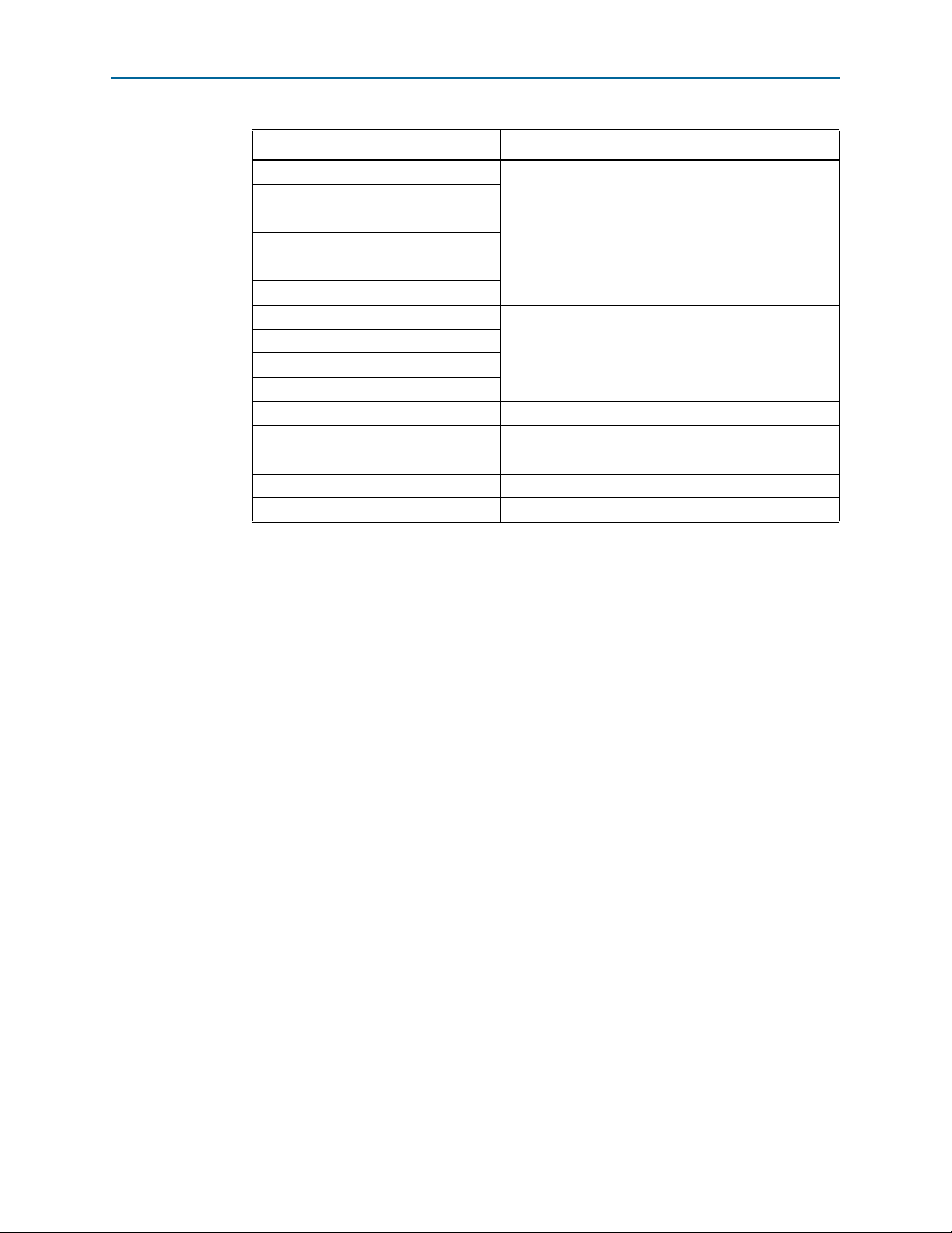
I/O Standards Support
I/O Standards Support
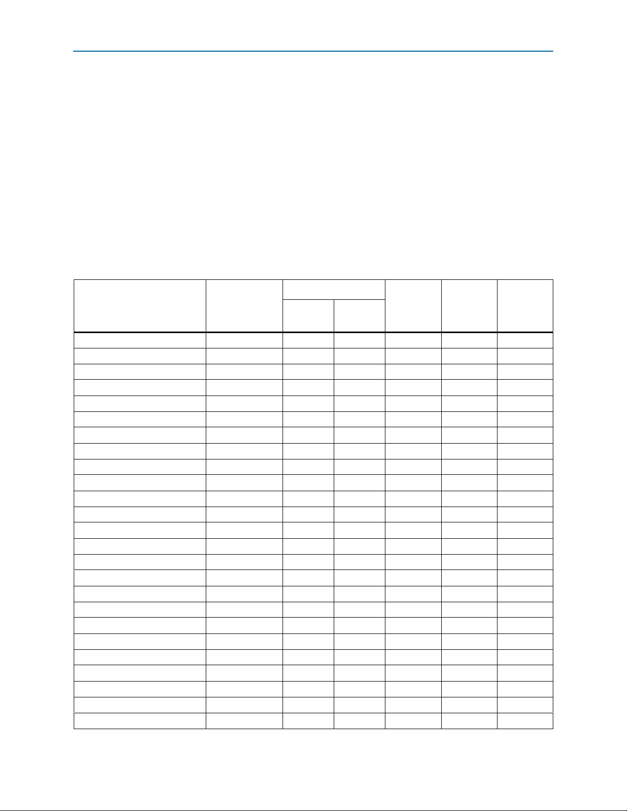
Tab le 5– 1 lists the supported I/O standards and typical power supply values
Table 5–1. Cyclone V I/O Standards and Voltage Levels
I/O Standard Standard Support
3.3-V LVTTL/3.3-V LVCMOS
3.0-V LVTTL/3.0-V LVCMOS
2.5-V LVCMOS
1.8-V LVCMOS
1.5-V LVCMOS
(2)
(2), (3)
(2)
(2)
(2)
JESD8-B 3.3/3.0/2.5 3.3 3.3 — —
JESD8-B 3.0/2.5 3.0 3.0 — —
JESD8-5 3.0/2.5 2.5 2.5 — —
JESD8-7 1.8/1.5 1.8 2.5 — —
JESD8-11 1.8/1.5 1.5 2.5 — —
(1)
(Part 1 of 2)
V
Input
Operation
(V) V
CCIO
Output
Operation
(V)
CCPD
(Pre-Driver
Voltage)
V
(V)
REF
(Input Ref
Voltage)
V
(Board
Termination
Voltage)
1.2-V LVCMOS JESD8-12 1.2 1.2 2.5 — —
3.0-V PCI
3.0-V PCI-X
SSTL-2 Class I JESD8-9B
SSTL-2 Class II JESD8-9B
SSTL-18 Class I
SSTL-18 Class II
SSTL-15 Class I
SSTL-15 Class II
SSTL-15 JESD79-3D
SSTL-135
SSTL-125
1.8-V HSTL Class I JESD8-6
1.8-V HSTL Class II JESD8-6
1.5-V HSTL Class I
1.5-V HSTL Class II
1.2-V HSTL Class I JESD8-16A
1.2-V HSTL Class II JESD8-16A
HSUL-12
Differential SSTL-2 Class I JESD8-9B
(4)
(3)
(3)
(4), (5)
(3)
PCI Rev. 2.2 3.0 3.0 3.0 — —
PCI-X Rev. 1.0 3.0 3.0 3.0 — —
(6)
(6)
(3)
(3)
(3)
(3)
JESD8-15
JESD8-15
—
—
—
—
(2)
(2)
JESD8-6
JESD8-6
—
(6)
(6)
(6)
(6)
(6)
(6)
(6)
(6)
(6)
(6)
(6)
(6)
(6)
(6)
(6)
2.5 2.5 1.25 1.25
2.5 2.5 1.25 1.25
1.8 2.5 0.90 0.90
1.8 2.5 0.90 0.90
1.5 2.5 0.75 0.75
1.5 2.5 0.75 0.75
1.5 2.5 0.75 —
1.35 2.5 0.675 —
1.25 2.5 0.625 —
1.8 2.5 0.90 0.90
1.8 2.5 0.90 0.90
1.5 2.5 0.75 0.75
1.5 2.5 0.75 0.75
1.2 2.5 0.6 0.6
1.2 2.5 0.6 0.6
1.2 2.5 0.6 —
2.5 2.5 — 1.25
TT
(V)
(7)
(7)
(7)
(7)
Cyclone V Device Handbook June 2012 Altera Corporation
Volume 1: Device Interfaces and Integration
Page 3
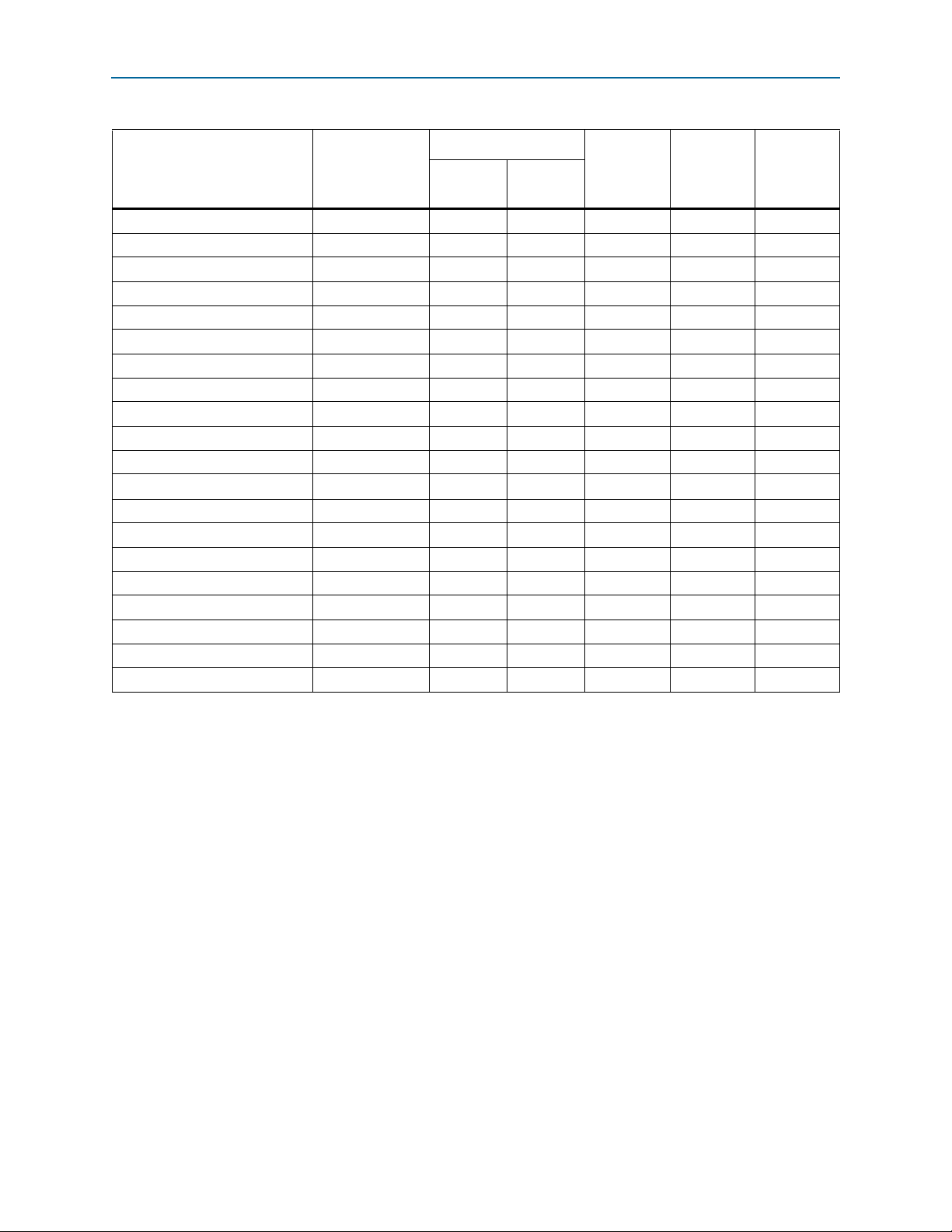
Chapter 5: I/O Features in Cyclone V Devices 5–3
I/O Standards Support
Table 5–1. Cyclone V I/O Standards and Voltage Levels
I/O Standard Standard Support
Differential SSTL-2 Class II JESD8-9B
Differential SSTL-18 Class I JESD8-15
Differential SSTL-18 Class II JESD8-15
Differential SSTL-15 Class I —
Differential SSTL-15 Class II —
Differential 1.8-V HSTL Class I JESD8-6
Differential 1.8-V HSTL Class II JESD8-6
Differential 1.5-V HSTL Class I JESD8-6
Differential 1.5-V HSTL Class II JESD8-6
Differential 1.2-V HSTL Class I JESD8-16A
Differential 1.2-V HSTL Class II JESD8-16A
Differential SSTL-15
JESD79-3D
Differential SSTL-135 —
Differential SSTL-125 —
Differential HSUL-12 —
LVDS ANSI/TIA/EIA-644
RSDS —
Mini-LVDS —
LVPECL
SLVS
(8)
(9)
—
JESD8-13
(1)
(Part 2 of 2)
V
Input
Operation
(6)
(6)
(6)
(6)
(6)
(6)
(6)
(6)
(6)
(6)
(6)
(6)
(6)
(6)
(6)
(6)
(6)
(6)
(6)
(6)
(V) V
CCIO
CCPD
(V)
(Pre-Driver
Output
Voltage)
Operation
2.5 2.5 — 1.25
1.8 2.5 — 0.90
1.8 2.5 — 0.90
1.5 2.5 — 0.75
1.5 2.5 — 0.75
1.8 2.5 — 0.90
1.8 2.5 — 0.90
1.5 2.5 — 0.75
1.5 2.5 — 0.75
1.2 2.5 — 0.60
1.2 2.5 — 0.60
1.5 2.5 — —
1.35 2.5 — —
1.25 2.5 — —
1.2 2.5 — —
2.5 2.5 — —
2.5 2.5 — —
2.5 2.5 — —
—2.5 — —
—2.5 — —
Notes to Table 5–1:
(1) You cannot assign SSTL, HSTL, and HSUL outputs on
(2) Supported in the hard processor system (HPS) column I/Os.
(3) Supported in the HPS row I/Os.
(4) The 3.3 V PCI and PCI-X I/O standards are not supported.
(5) PCI-X does not meet the PCI-X I-V curve requirement at the linear region.
(6) Single-ended HSTL/SSTL/HSUL, differential SSTL/HSTL/HSUL, and LVD S input buffers are powered by V
(7) This I/O standard typically does not require board termination.
(8) The support for the LVPECL I/O standard is only for input clock operation.
(9) The support for the SLVS I/O standard is only for input operation.
VREF
pins, even if there are no SSTL, HSTL, and HSUL inputs in the bank.
(Input Ref
Voltage)
.
CCPD
V
(V)
V
(V)
REF
TT
(Board
Termination
Voltage)
(7)
(7)
(7)
(7)
June 2012 Altera Corporation Cyclone V Device Handbook
Volume 1: Device Interfaces and Integration
Page 4

5–4 Chapter 5: I/O Features in Cyclone V Devices
Design Considerations
Design Considerations
There are several considerations that require your attention to ensure the success of
your designs.
f For more information about absolute maximum rating and maximum allowed
overshoot during transitions, refer to the Cyclone V Device Datasheet.
I/O Bank Restrictions
The following sections provide guidelines for mixing non-voltage-referenced and
voltage-referenced I/O standards in the devices.
Non-Voltage-Referenced Standards
Each Cyclone V I/O bank has its own
1.25, 1.35, 1.5, 1.8, 2.5, 3.0, or 3.3 V). An I/O bank can simultaneously support any
number of input signals with different I/O standard assignments if the I/O standards
support the V
level of the I/O bank.
CCIO
For output signals, a single I/O bank supports non-voltage-referenced output signals
that drive at the same voltage as V
value, it can only drive out the value for non-voltage-referenced signals.
VCCIO
pins and supports only one V
. Because an I/O bank can only have one V
CCIO
CCIO
(1.2,
CCIO
For example, an I/O bank with a 2.5-V V
setting can support 2.5-V standard
CCIO
inputs and outputs, and 3.0-V LVCMOS inputs only.
Voltage-Referenced Standards
To accommodate voltage-referenced I/O standards, each Cyclone V I/O bank
contains a dedicated
and a single voltage reference (V
VREF
pin. Each bank can have only a single V
) level.
REF
voltage level
CCIO
An I/O bank featuring single-ended or differential standards can support different
voltage-referenced standards if the V
Voltage-referenced bidirectional and output signals must be the same as the V
CCIO
and V
are the same levels.
REF
CCIO
voltage of the I/O bank.
For example, you can place only SSTL-2 output pins in an I/O bank with a
2.5-V V
CCIO
.
Mixing Voltage-Referenced and Non-Voltage-Referenced Standards
An I/O bank can support voltage-referenced and non-voltage-referenced pins by
applying each of the rule sets individually.
First example: an I/O bank can support SSTL-18 inputs and outputs, and 1.8-V inputs
and outputs with a 1.8-V V
Second example: an I/O bank can support 1.5-V standards, 1.8-V inputs (but not
outputs), and 1.5-V HSTL I/O standards with a 1.5-V V
and a 0.9-V V
CCIO
REF
.
and 0.75-V V
CCIO
REF
.
Cyclone V Device Handbook June 2012 Altera Corporation
Volume 1: Device Interfaces and Integration
Page 5

Chapter 5: I/O Features in Cyclone V Devices 5–5
Design Considerations
V
Restriction
CCPD
One
VCCPD
pin is shared in a group of I/O banks. The V
grouping on Cyclone V
CCPD
are as follows. Each line item is a separate group:
■ BANK 3A
■ BANK3B + BANK4A
■ BANK5A
■ BANK5B
■ BANK6A
■ BANK7A + BANK8A
First example: if one I/O bank in a group uses 3.0-V V
same group must also use 3.0-V V
same group to also use a 3.0-V V
Second example: if one I/O bank in a group uses a 2.5-V V
same group must also use 2.5-V V
V
CCIO
V
Restriction
CCIO
When planning the I/O bank usage, you must ensure the V
with the V
power pin. This limits the possible V
VCCPD
First example: if
4A can be connected to any of the following voltages: 1.2 V, 1.25 V, 1.35 V, 1.5 V, 1.8 V,
or 2.5 V.
Second example: if
4A must also be connected to 3.0 V.
V
Pin Restriction
REF
You cannot assign shared
, other I/O banks in the
CCPD
. This would also require each I/O bank in the
CCPD
.
CCIO
, other I/O banks in the
CCPD
. However, each I/O bank can use different
CCPD
voltages provided they are 1.2, 1.25, 1.35, 1.5, 1.8, or 2.5 V.
CCIO
voltage of the same bank. Some banks may share the same
CCPD
voltages that can be used on banks that share
CCIO
power pins.
VCCPD3B
is connected to 2.5 V, then the
VCCPD3B
is connected to 3.0 V, then the
VREF
pins as LVD S or external memory interface pins.
VCCIO
pins for banks 3B and
VCCIO
voltage is compatible
VCCPD
pins for banks 3B and
SSTL, HSTL, and HSUL I/O standards do not support shared
For example, if a particular
B1p/B1n
Shared
pin pair do not have LVDS transmitter support.
VREF
pins will have reduced performance when used as normal I/Os. You
B1p
or
B1n
pin is a shared
VREF
must perform SI analysis using your board design to determine the F
VREF
pins.
pin, the corresponding
for your
MAX
system.
3.3-V I/O Interface
To ensure device reliability and proper operation when you use the Cyclone V device
for 3.3-V I/O interfacing, do not violate the absolute maximum ratings of the device.
For a transmitter, use slow slew-rate and series termination to limit the overshoot and
undershoot at the I/O pins.
June 2012 Altera Corporation Cyclone V Device Handbook
Volume 1: Device Interfaces and Integration
Page 6

5–6 Chapter 5: I/O Features in Cyclone V Devices
For a receiver, use the on-chip clamp diode to limit the overshoot and undershoot
voltage at the I/O pins.
f For more information about absolute maximum rating and maximum allowed
overshoot during transitions, refer to the Cyclone V Device Datasheet.
1 Altera recommends that you perform IBIS or SPICE simulations to make sure the
overshoot and undershoot voltages are within the specifications.
Design Considerations
LVDS Channels
For LV DS applications, you must use the phase-locked loops (PLLs) in integer PLL
mode.
Differential Pin Placement
When you use LVD S channels, adhere to the guidelines in the following sections.
The Quartus
message if the guidelines are not followed to ensure proper high-speed operation.
®
II compiler automatically checks the design and issues an error
For more information about the Cyclone V device high-speed differential I/O
interfaces, refer to “High-Speed Differential I/O Interfaces” on page 5–36.
LVDS Channel Driving Distance
Each PLL can drive all the LVD S channels in the entire quadrant.
Using Corner and Center PLLs
You can use a corner PLL to drive all transmitter channels and a center PLL to drive
all LV DS receiver channels in the same I/O bank.
A corner PLL and a center PLL can drive duplex channels in the same I/O quadrant if
the channels that are driven by each PLL are not interleaved.
You do not require separation between the group of channels that are driven by the
corner and center, left and right PLLs.
Cyclone V Device Handbook June 2012 Altera Corporation
Volume 1: Device Interfaces and Integration
Page 7
Chapter 5: I/O Features in Cyclone V Devices 5–7
Design Considerations
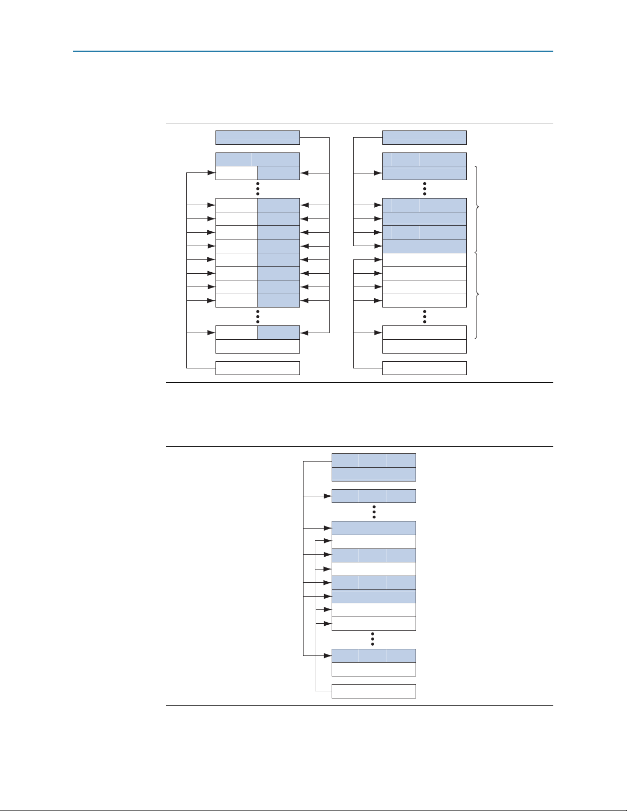
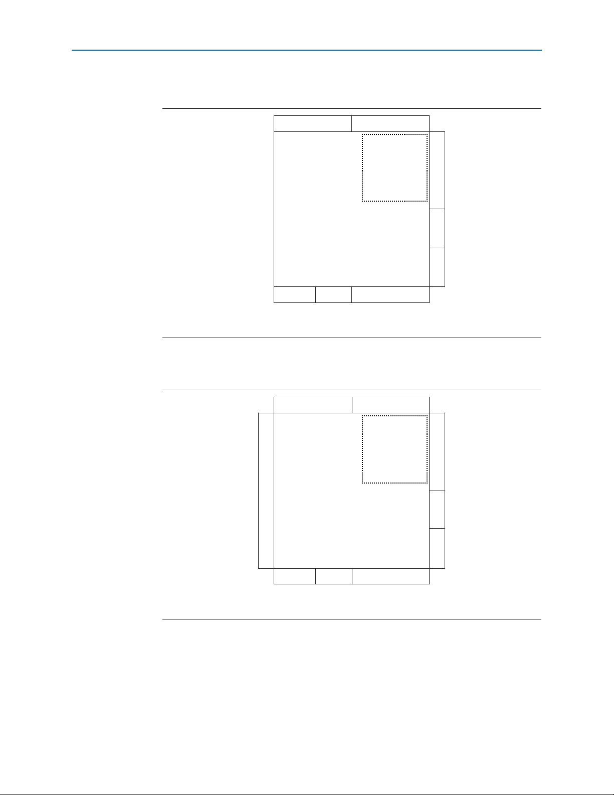
Figure 5–1 shows two different PLLs driving a transmitter channel and a receiver
channel in the same LVD S module.
3
Figure 5–1. Corner and Center PLLs Driving LVDS Differential I/Os in the Same Quadrant
Corner PLL
Reference CLK
Diff RX Diff TX
Diff RX Diff TX
Diff RX Diff TX
Diff RX Diff TX
Diff RX Diff TX
Diff RX Diff TX
Diff RX Diff TX
Diff RX Diff TX
Diff RX Diff TX
Diff RX Diff TX
Reference CLK
Center PLL
Corner PLL
Reference CLK
LVDS I/O
LVDS I/O
LVDS I/O
LVDS I/O
LVDS I/O
LVDS I/O
LVDS I/O
LVDS I/O
LVDS I/O
LVDS I/O
Reference CLK
Center PLL
Channels Driven
by Corner PLL
No Separation
Buffer Needed
Channels Driven
by Center PLL
Figure 5–2. shows invalid placement of the LVD S I/Os.
Figure 5–2. Invalid Placement of LVDS I/Os Due to Interleaving of Channels Driven by the Corner
and Center PLLs
Corner PLL
Reference CLK
LVDS I/O
LVDS I/O
LVDS I/O
LVDS I/O
LVDS I/O
LVDS I/O
LVDS I/O
LVDS I/O
LVDS I/O
LVDS I/O
Reference CLK
Center PLL
June 2012 Altera Corporation Cyclone V Device Handbook
Volume 1: Device Interfaces and Integration
Page 8
5–8 Chapter 5: I/O Features in Cyclone V Devices
I/O Banks
I/O Banks
The number of Cyclone V I/O banks in a particular device depends on the device
density.
Each I/O bank can simultaneously support multiple I/O standards.
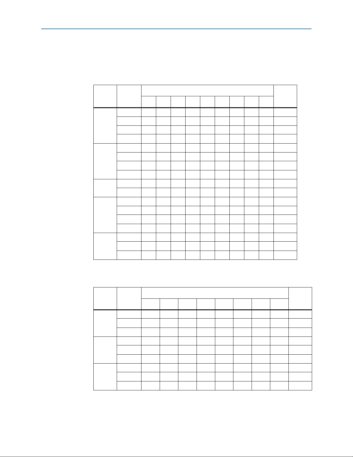
Figure 5–3 shows the I/O banks in Cyclone V E devices.
Figure 5–3. I/0 Banks for Cyclone V E Devices
Bank 8A
Bank 2A
Note to Figure 5–3:
(1) This is a top view of the silicon die that corresponds to a reverse view of the device package.
(1)
Bank 7A
Bank 6A
Bank 5BBank 5A
Bank 3BBank 3A
Bank 4A
Figure 5–4 shows the I/O banks in Cyclone V GX and GT devices.
Figure 5–4. I/0 Banks for Cyclone V GX and GT Devices
(1)
Bank 8A
Transceiver Block
Bank 3BBank 3A
Note to Figure 5–4:
(1) This is a top view of the silicon die that corresponds to a reverse view of the device package.
Cyclone V Device Handbook June 2012 Altera Corporation
Volume 1: Device Interfaces and Integration
Bank 7A
Bank 6A
Bank 5BBank 5A
Bank 4A
Page 9
Chapter 5: I/O Features in Cyclone V Devices 5–9
I/O Banks
Figure 5–5 shows the I/O banks in Cyclone V SE devices.
Figure 5–5. I/0 Banks for Cyclone V SE Devices
Bank 8A HPS Column I/O
(1)
HPS Core
HPS Row I/OBank 5BBank 5A
Bank 3BBank 3A
Bank 4A
Note to Figure 5–5:
(1) This is a top view of the silicon die that corresponds to a reverse view of the device package.
Figure 5–6 shows the I/O banks in Cyclone V SX and ST devices.
Figure 5–6. I/0 Banks for Cyclone V SX and ST Devices
(1)
Bank 8A HPS Column I/O
HPS Core
HPS Row I/OBank 5BBank 5A
Transceiver Block
Bank 3BBank 3A
Note to Figure 5–6:
(1) This is a top view of the silicon die that corresponds to a reverse view of the device package.
Bank 4A
June 2012 Altera Corporation Cyclone V Device Handbook
Volume 1: Device Interfaces and Integration
Page 10
5–10 Chapter 5: I/O Features in Cyclone V Devices
I/O Banks
Modular I/O Banks
The I/O pins in Cyclone V devices are arranged in groups called modular I/O banks.
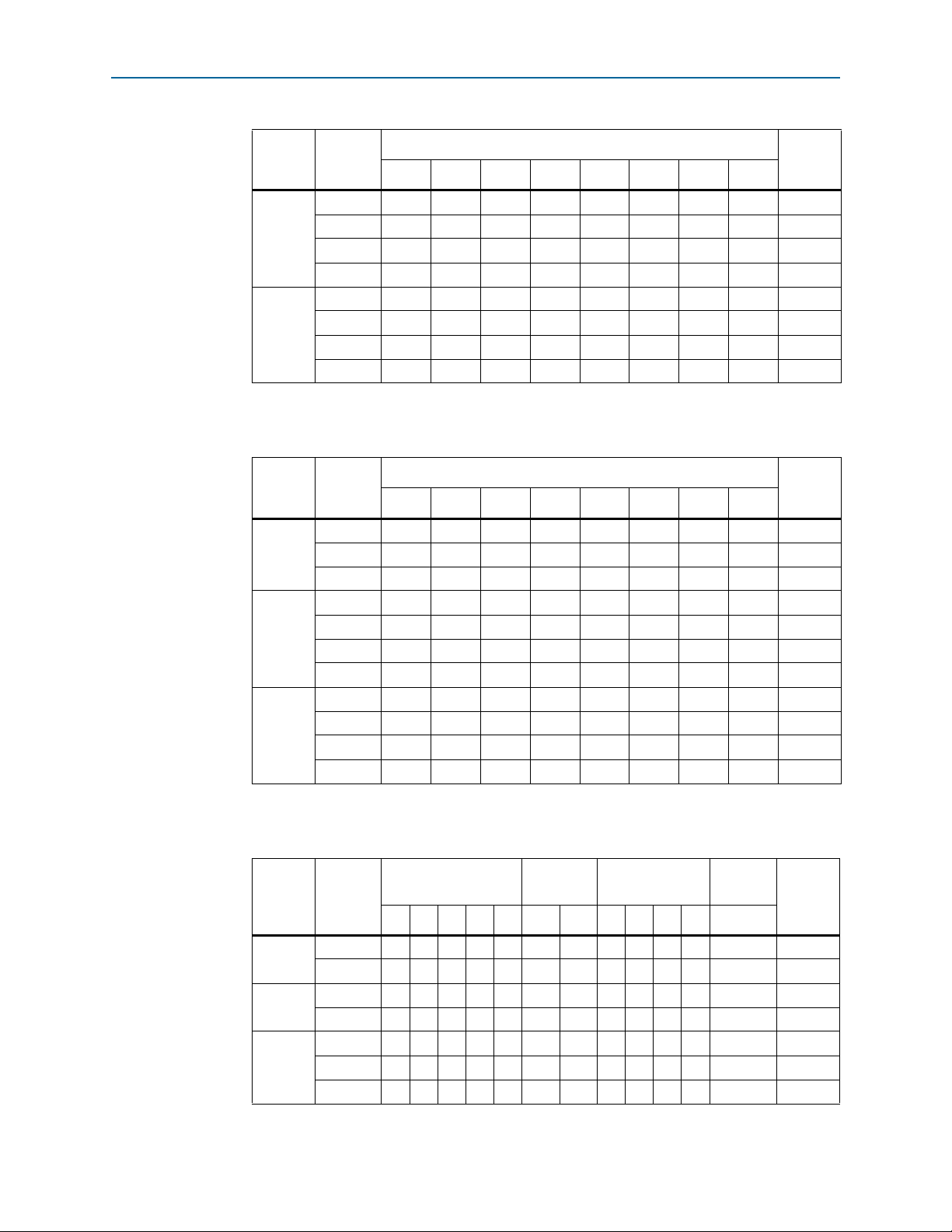
Tab le 5 –2 list the modular I/O banks for Cyclone V E devices.
Table 5–2. Modular I/O Banks for Cyclone V E Devices —Preliminary
Member
Code
A2
A4
A5
A7
A9
Package
Tot al
2A 3A 3B 4A 5A 5B 6A 7A 8A
F256 16 16 16 16 16 16 — 16 16 128
U324 32 16 16 32 16 16 — 32 16 176
U484 16 16 32 48 16 16 — 48 32 224
F484 16 16 32 48 16 16 — 48 32 224
F256 16 16 16 16 16 16 — 16 16 128
U324 32 16 16 32 16 16 — 32 16 176
U484 16 16 32 48 16 16 — 48 32 224
F484 16 16 32 48 16 16 — 48 32 224
U484 —1632481632—4832 224
F484 —1632481616—8032 240
U484 —1632481648—4832 240
F484 —1632481616—8032 240
F672 —1632801664168032 336
F896 —3248803248808080 480
F484 —1632481616—6432 224
F672 —1632801632488032 336
F896 —3248803248808080 480
FPGA I/O Bank
Tab le 5 –3 list the modular I/O banks for Cyclone V GX devices.
Table 5–3. Modular I/O Banks for Cyclone V GX Devices (Part 1 of 2)—Preliminary
Member
Code
Package
3A 3B 4A 5A 5B 6A 7A 8A
FPGA I/O Bank
Total
U324 TBD TBD TBD TBD TBD TBD TBD TBD TBD
C3
U484 16 32 48 16 16 — 48 32 208
F484 16 32 48 16 16 — 48 32 208
U484 16 32 48 16 32 — 48 32 224
C4
F484 16 32 48 16 16 — 80 32 240
F672 16 32 80 16 64 16 80 32 336
U484 16 32 48 16 32 — 48 32 224
C5
F484 16 32 48 16 16 — 80 32 240
F672 16 32 80 16 64 16 80 32 336
Cyclone V Device Handbook June 2012 Altera Corporation
Volume 1: Device Interfaces and Integration
Page 11
Chapter 5: I/O Features in Cyclone V Devices 5–11
I/O Banks
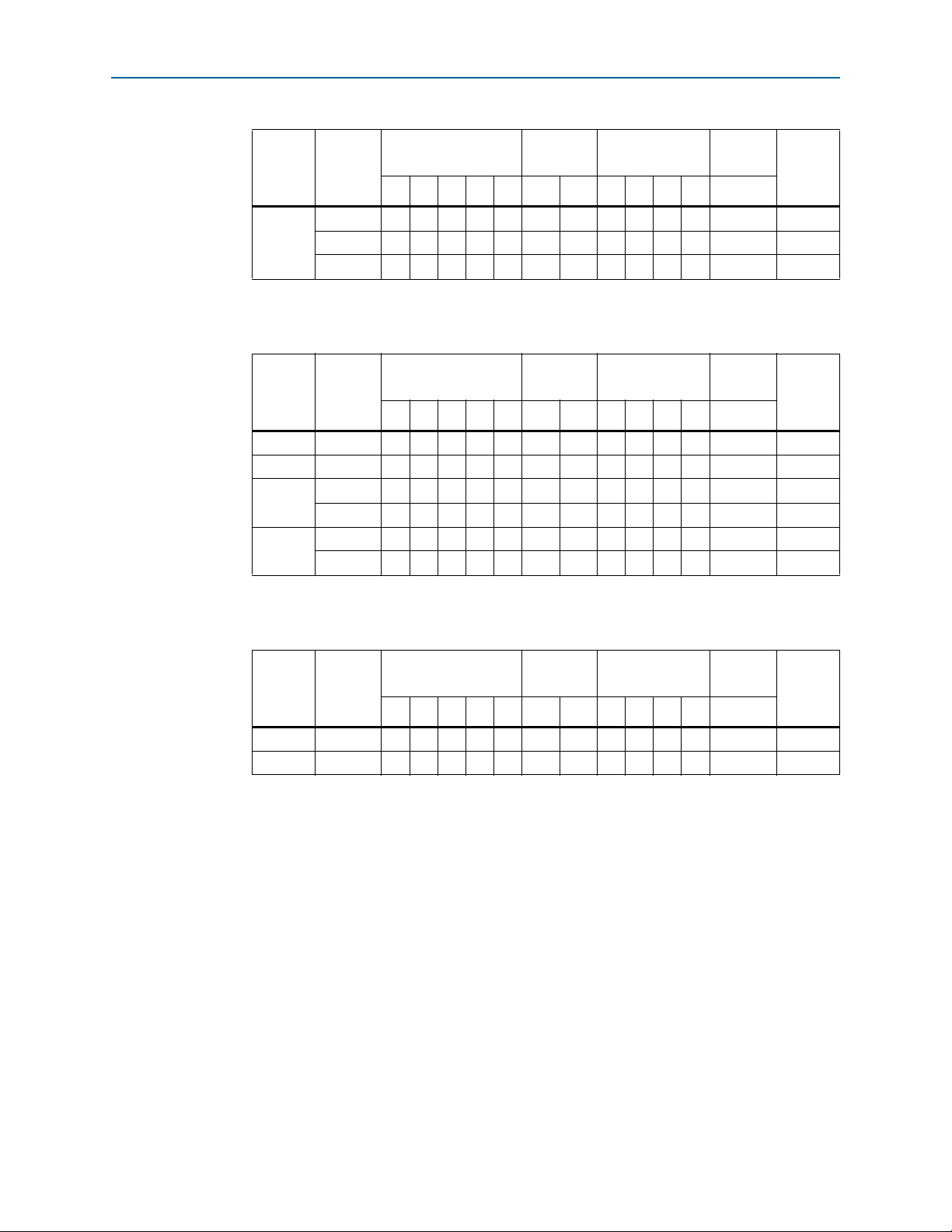
Table 5–3. Modular I/O Banks for Cyclone V GX Devices (Part 2 of 2)—Preliminary
Member
Code
Package
3A 3B 4A 5A 5B 6A 7A 8A
FPGA I/O Bank
U484 16 32 48 16 48 — 48 32 240
C7
F484 16 32 48 16 16 — 80 32 240
F672 16 32 80 16 64 16 80 32 336
F896 32 48 80 32 48 80 80 80 480
F484 16 32 48 16 16 — 64 32 224
C9
F672 16 32 80 16 32 48 80 32 336
F896 32 48 80 32 48 80 80 80 480
F1152 TBD TBD TBD TBD TBD TBD TBD TBD TBD
Tab le 5 –4 list the modular I/O banks for Cyclone V GT devices.
Table 5–4. Modular I/O Banks for Cyclone V GT Devices —Preliminary
Member
Code
Package
3A 3B 4A 5A 5B 6A 7A 8A
FPGA I/O Bank
U484 16 32 48 16 32 — 48 32 224
D5
F484 16 32 48 16 16 — 80 32 240
F672 16 32 80 16 64 16 80 32 336
U484 16 32 48 16 48 — 48 32 240
D7
F484 16 32 48 16 16 — 80 32 240
F672 16 32 80 16 64 16 80 32 336
F896 32 48 80 32 48 80 80 80 480
F484 16 32 48 16 16 — 64 32 224
D9
F672 16 32 80 16 32 48 80 32 336
F896 32 48 80 32 48 80 80 80 480
F1152 TBD TBD TBD TBD TBD TBD TBD TBD TBD
Total
Total
Tab le 5 –5 list the modular I/O banks for Cyclone V SE devices.
Table 5–5. Modular I/O Banks for Cyclone V SE Devices (Part 1 of 2)—Preliminary
Member
Code
Package
FPGA I/O Bank
HPS Row
I/O Bank
HPS Column I/O
Bank
FPGA I/O
Bank
Total
3A 3B 4A 5A 5B 6A 6B 7A 7B 7C 7D 8A
A2
A4
U484 16 6 22 16 — 52 23 19 21 8 14 6 203
U672 16 32 68 16 — 56 44 19 22 12 14 13 312
U484 16 6 22 16 — 52 23 19 21 8 14 6 203
U672 16 32 68 16 — 56 44 19 22 12 14 13 312
U484 16 6 22 16 — 52 23 19 21 8 14 6 203
A5
U672 16 32 68 16 — 56 44 19 22 12 14 13 312
F896 32 48 80 32 16 56 44 19 22 12 14 80 455
June 2012 Altera Corporation Cyclone V Device Handbook
Volume 1: Device Interfaces and Integration
Page 12
5–12 Chapter 5: I/O Features in Cyclone V Devices
I/O Banks
Table 5–5. Modular I/O Banks for Cyclone V SE Devices (Part 2 of 2)—Preliminary
Member
Code
Package
FPGA I/O Bank
HPS Row
I/O Bank
HPS Column I/O
Bank
FPGA I/O
Bank
3A 3B 4A 5A 5B 6A 6B 7A 7B 7C 7D 8A
U484 16 6 22 16 — 52 23 19 21 8 14 6 203
A6
U672 16 32 68 16 — 56 44 19 22 12 14 13 312
F896 32 48 80 32 16 56 44 19 22 12 14 80 455
Tab le 5 –6 list the modular I/O banks for Cyclone V SX devices.
Table 5–6. Modular I/O Banks for Cyclone V SX Devices —Preliminary
Member
Code
Package
FPGA I/O Bank
HPS Row
I/O Bank
HPS Column I/O
Bank
FPGA I/O
Bank
3A 3B 4A 5A 5B 6A 6B 7A 7B 7C 7D 8A
C2 U672 16 32 68 16 — 56 44 19 22 12 14 13 312
C4 U672 16 32 68 16 — 56 44 19 22 12 14 13 312
C5
C6
U672 16 32 68 16 — 56 44 19 22 12 14 13 312
F896 32 48 80 32 16 56 44 19 22 12 14 80 455
U672 16 32 68 16 — 56 44 19 22 12 14 13 312
F896 32 48 80 32 16 56 44 19 22 12 14 80 455
Total
Total
Tab le 5 –7 list the modular I/O banks for Cyclone V ST devices.
Table 5–7. Modular I/O Banks for Cyclone V ST Devices —Preliminary
Member
Code
Package
FPGA I/O Bank
HPS Row
I/O Bank
HPS Column I/O
Bank
FPGA I/O
Bank
3A 3B 4A 5A 5B 6A 6B 7A 7B 7C 7D 8A
D5 F896 32 48 80 32 16 56 44 19 22 12 14 80 455
D6 F896 32 48 80 32 16 56 44 19 22 12 14 80 455
Total
Cyclone V Device Handbook June 2012 Altera Corporation
Volume 1: Device Interfaces and Integration
Page 13
Chapter 5: I/O Features in Cyclone V Devices 5–13
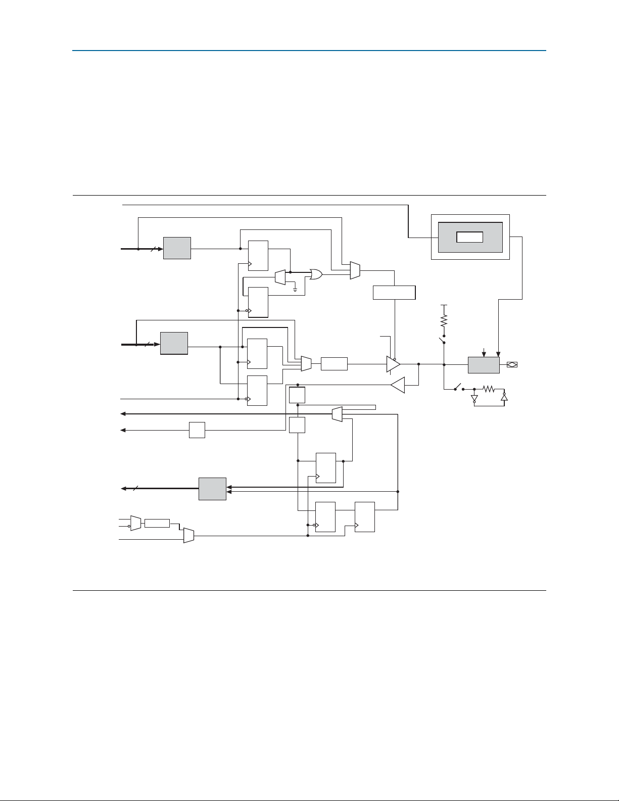
IOE Features
IOE Features
The IOEs in Cyclone V devices contain a bidirectional I/O buffer and I/O registers to
support a complete embedded bidirectional single data rate (SDR) or double data rate
(DDR) transfer.
The IOEs are located in I/O blocks around the periphery of the Cyclone V device.
Figure 5–7 shows the Cyclone V IOE structure.
Figure 5–7. IOE Structure for Cyclone V Devices
From Core
OE
from
Core
Write
Data
from
Core
clkout
To
Core
To
Core
Read
Data
to
Core
DQS
CQn
clkin
2
Half Data
Rate Block
Half Data
4
Rate Block
D3_1
Delay
4
D4 Delay
Read
FIFO
OE Register
PRN
DQ
OE Register
PRN
DQ
Output Register
PRN
DQ
Output Register
PRN
DQ
(1), (2)
D3_0
Delay
D1
Delay
D5 Delay
Input Register
PRN
DQ
Input Register
PRN
Q
D
Programmable
Current
Strength and
Slew Rate
Control
Open Drain
Input Register
PRN
Q
D
D5 Delay
Output Buffer
Input Buffer
DQS Logic Block
D5_OCT
Dynamic OCT Control
V
CCIO
Programmable
Pull-Up Resistor
From OCT
Calibration
Block
On-Chip
Termination
Bus-Hold
Circuit
(2)
Notes to Figure 5–7:
(1) The D3_0 and D3_1 delays have the same available settings in the Quartus II software.
(2) One dynamic OCT control is available for each DQ/DQS group.
June 2012 Altera Corporation Cyclone V Device Handbook
Volume 1: Device Interfaces and Integration
Page 14
5–14 Chapter 5: I/O Features in Cyclone V Devices
IOE Features
Current Strength
You can use the programmable current strength to mitigate the effects of high signal
attenuation that is caused by a long transmission line or a legacy backplane.
The output buffer for each Cyclone V device I/O pin has a programmable current
strength control for the following I/O standards.
Tab le 5 –8 lists the programmable current strength settings for Cyclone V devices.
Table 5–8. Programmable Current Strength Settings —Preliminary
I/O Standard I
3.3-V LVTTL
(2)
3.3-V LVCMOS
3.0-V LVTTL
(2)
3.0-V LVCMOS
2.5-V LVCMOS
1.8-V LVCMOS
1.5-V LVCMOS
(2)
(2)
(2)
(2)
(2)
Current Strength Setting (mA)
OH/IOL
(3)
16
, 8, 4
2
16, 12, 8, 4
16, 12, 8, 4
16, 12, 8, 4
12, 10, 8, 6, 4, 2
12, 10, 8, 6, 4, 2
1.2-V LVCMOS 8, 6, 4, 2
SSTL-2 Class I 12, 10, 8
SSTL-2 Class II 16
SSTL-18 Class I
SSTL-18 Class II
SSTL-15 Class I
SSTL-15 Class II
(2)
(2)
(2)
(2)
12, 10, 8, 6, 4
16
12, 10, 8, 6, 4
16
1.8-V HSTL Class I 12, 10, 8, 6, 4
1.8-V HSTL Class II 16
1.5-V HSTL Class I
1.5-V HSTL Class II
(2)
(2)
12, 10, 8, 6, 4
16
1.2-V HSTL Class I 12, 10, 8, 6, 4
1.2-V HSTL Class II 16
Notes to Table 5–8:
(1) The default current strength setting in the Quartus II software is the current strength shown in bold.
(2) Supported in HPS.
(3) Not Supported in HPS.
(1)
1 Altera recommends that you perform IBIS or SPICE simulations to determine the best
current strength setting for your specific application.
Cyclone V Device Handbook June 2012 Altera Corporation
Volume 1: Device Interfaces and Integration
Page 15
Chapter 5: I/O Features in Cyclone V Devices 5–15
IOE Features
MultiVolt I/O Interface
The MultiVolt I/O interface feature that allows Cyclone V devices in all packages to
interface with systems of different supply voltages.
Tab le 5 –9 lists Cyclone V MultiVolt I/O support.
Table 5–9. MultiVolt I/O Support in Cyclone V Devices
V
CCIO
(V)
1.2 1.25 1.35 1.5 1.8 2.5 3.0 3.3 1.2 1.25 1.35 1.5 1.8 2.5 3.0 3.3
Input Signal (V) Output Signal (V)
(1), (2)
1.2 Y ————— — — Y ———————
1.25— Y ———— — — — Y ——————
1.35—— Y ——— — — —— Y —————
1.5 ——— Y Y — — — ——— Y ————
1.8 ——— Y Y — — — ———— Y ———
2.5 ————— Y Y
3.0 ————— Y Y
3.3 ————— Y Y
(3)
(3)
(3)
Notes to Table 5–9:
(1) The pin current may be slightly higher than the default value. Verify that the VOL maximum and VOH minimum voltages of the driving device do
not violate the applicable V
(2) For V
(3) Altera recommends using the on-chip clamp diode on the I/O pins when the input signal is 3.0 V or 3.3 V.
= 1.2, 1.25, 1.35, 1.5, 1.8, and 2.5 V, V
CCIO
maximum and VIH minimum voltage specifications of the Cyclone V device.
IL
= 2.5 V. For V
CCPD
(3)
Y
(3)
Y
(3)
Y
= 3.0 V, V
CCIO
————— Y ——
—————— Y —
——————— Y
= 3.0 V. For V
CCPD
= 3.3 V, V
CCIO
CCPD
= 3.3 V.
June 2012 Altera Corporation Cyclone V Device Handbook
Volume 1: Device Interfaces and Integration
Page 16
5–16 Chapter 5: I/O Features in Cyclone V Devices
Programmable IOE Features
Programmable IOE Features
The Cyclone V I/O supports programmable features, as listed in Table 5–10.
(1)
2 = high
(1)
OCT feature.
S
—
For LVDS I/O standard only. Not supported for
differential HSTL and SSTL I/O standards.
—
Table 5–10. Supported I/O Features and Settings
Feature Setting Condition
Slew Rate Control 0 = Slow, 1 = Fast (default) Disabled when you use the R
I/O Delay
Open-Drain Output On, Off (default) —
Bus-Hold On, Off (default) Disabled when you use the weak pull-up resistor feature.
Weak Pull-up Resistor On, Off (default) Disabled when you use the bus-hold feature.
Pre-Emphasis 0 = Disabled, 1 = Enabled (default)
Differential Output Voltage
On-Chip Clamp Diode
Notes to Table 5–10:
(1) For information about the programmable IOE features, refer to the Cyclone V Device Datasheet.
(2) The PCI on-chip clamp diode is available on all general purpose I/O (GPIO) pins in all Cyclone V device variants.
(2)
0 = low, 1 = medium (default),
On, Off (default) Recommended to turn on for 3.3-V I/O standards
Slew-Rate Control
The programmable output slew-rate control in the output buffer of each regular- and
dual-function I/O pin allows you to configure the following:
■ Fast slew rate—provides high-speed transitions for high-performance systems.
■ Slow slew rate—reduces system noise and crosstalk but adds a nominal delay to
the rising and falling edges.
You can specify the slew rate on a pin-by-pin basis because each I/O pin contains a
slew-rate control.
1 Altera recommends that you perform IBIS or SPICE simulations to determine the best
slew rate setting for your specific application.
I/O Delay
The following sections describe the programmable IOE delay and the programmable
output buffer delay.
Programmable IOE Delay
You can activate the programmable delays to ensure zero hold times, minimize setup
times, or increase clock-to-output times.
This feature helps read and write timing margins because it minimizes the
uncertainties between signals in the bus.
Each pin can have a different input delay from pin-to-input register or a delay from
output register-to-output pin values to ensure that the signals within a bus have the
same delay going into or out of the device.
Cyclone V Device Handbook June 2012 Altera Corporation
Volume 1: Device Interfaces and Integration
Page 17

Chapter 5: I/O Features in Cyclone V Devices 5–17
Programmable IOE Features
f For more information about programmable IOE delay specifications, refer to the
Cyclone V Device Datasheet.
Programmable Output Buffer Delay
The device supports delay chains built inside the single-ended output buffer.
There are four levels of output buffer delay settings. By default, there is no delay.
The following actions allow you to independently control the rising and falling edge
delays of the output buffer:
■ Adjust the output-buffer duty cycle
■ Compensate channel-to-channel skew
■ Reduce simultaneous switching output (SSO) noise by deliberately introducing
channel-to-channel skew
■ Improve high-speed memory-interface timing margins
f For more information about programmable output buffer delay specifications, refer to
the Cyclone V Device Datasheet.
Open-Drain Output
The optional open-drain output for each I/O pin is equivalent to an open collector
output.
When configured as an open drain, the logic value of the output is either high-Z or
logic low.
Use an external resistor to pull the signal to a logic high.
Bus-Hold
Each I/O pin provides an optional bus-hold feature that is active only after
configuration. When the device enters user mode, the bus-hold circuit captures the
value that is present on the pin by the end of the configuration.
The bus-hold circuitry uses a resistor with a nominal resistance (R
7k
Ω, to weakly pull the signal level to the last-driven state of the pin. The bus-hold
circuitry holds this pin state until the next input signal is present. Because of this, you
do not require an external pull-up or pull-down resistor to hold a signal level when
the bus is tri-stated.
For each I/O pin, you can individually specify that the bus-hold circuitry pulls
non-driven pins away from the input threshold voltage—where noise can cause
unintended high-frequency switching. To prevent over-driving signals, the bus-hold
circuitry drives the voltage level of the I/O pin lower than the V
If you enable the bus-hold feature, you cannot use the programmable pull-up option.
To configure the I/O pin for differential signals, disable the bus-hold feature.
), approximately
BH
level.
CCIO
June 2012 Altera Corporation Cyclone V Device Handbook
Volume 1: Device Interfaces and Integration
Page 18

5–18 Chapter 5: I/O Features in Cyclone V Devices
Programmable IOE Features
Pull-Up Resistor
The pull-up resistor weakly holds the I/O to the V
The Cyclone V device supports programmable weak pull-up resistors only on user
I/O pins but not on dedicated configuration pins, JTAG pins, or dedicated clock pins.
Each I/O pin provides an optional programmable pull-up resistor during user mode.
If you enable this option, you cannot use the bus-hold feature.
Pre-Emphasis
Pre-emphasis boosts the output current momentarily.
The overshoot introduced by the extra current happens only during a change of state
switching to increase the output slew rate and does not ring, unlike the overshoot
caused by signal reflection.
The V
a high-speed transmission signal. At a high frequency, the slew rate may not be fast
enough to reach the full V
jitter.
The amount of pre-emphasis required depends on the attenuation of the
high-frequency component along the transmission line.
For more information, refer to “Programmable Pre-Emphasis” on page 5–48.
level.
CCIO
setting and the output impedance of the driver set the output current limit of
OD
level before the next edge, producing pattern-dependent
OD
Differential Output Voltage
The Cyclone V LV DS transmitters support programmable VOD.
The programmable V
optimize the trace length and power consumption. A higher V
voltage margins at the receiver end, and a smaller V
consumption.
For more information, refer to “Programmable V
f For the weak pull-up resistor value, refer to the Cyclone V Device Datasheet.
settings allow you to adjust the output eye opening to
OD
OD
swing reduces power
OD
” on page 5–47.
OD
swing improves
Cyclone V Device Handbook June 2012 Altera Corporation
Volume 1: Device Interfaces and Integration
Page 19

Chapter 5: I/O Features in Cyclone V Devices 5–19
OCT Schemes
OCT Schemes
Dynamic RS and RT OCT provides I/O impedance matching and termination
capabilities. OCT maintains signal quality, saves board space, and reduces external
component costs.
Cyclone V devices support OCT in all I/O banks.
Tab le 5 –11 lists the OCT schemes supported in Cyclone V devices.
Table 5–11. OCT Schemes in Cyclone V
Direction OCT Schemes
OCT R
with calibration
Output
Input
S
OCT RS without calibration
OCT R
with calibration
T
OCT RD (LVDS I/O standard only)
Bidirectional Dynamic OCT R
Note to Tab le 5 –11:
(1) For information about OCT support for the selectable I/O standards, refer to Table 5–12.
(1)
(1)
and OCT R
S
(1)
T
June 2012 Altera Corporation Cyclone V Device Handbook
Volume 1: Device Interfaces and Integration
Page 20

5–20 Chapter 5: I/O Features in Cyclone V Devices
OCT Schemes
OCT Calibration Block
You can calibrate the OCT using any of the available three OCT calibration blocks for
each device. Each calibration block contains one
RZQ
pin.
Figure 5–8 shows the location of I/O banks with OCT calibration blocks and
Figure 5–8. OCT Calibration Block and RZQ Pin Location
RZQ pin
Bank 8A
Transceiver Block
Bank 3BBank 3A
(1)
—Preliminary
Bank 7A
Calibration block
Bank 4A
Bank 6A
Bank 5BBank 5A
RZQ pin
RZQ
pins.
RZQ pin
Note to Figure 5–8:
(1) This is a top view of the silicon die that corresponds to a reverse view of the device package. This figure illustrates
the highest density for Cyclone V devices.
You c a n use R
and R
OCT use the same V
T
and RT OCT in the same I/O bank for different I/O standards if the RS
S
supply voltage. You cannot configure the RSOCT and
CCIO
the programmable current strength for the same I/O buffer.
Connect the
RZQ
pin shares the same V
RZQ
pin to the GND pin through a resistor with the specified value. The
supply voltage with the I/O bank where the pin is
CCIO
located.
Cyclone V devices support calibrated R
and calibrated RT on all I/O pins except for
S
dedicated configuration pins.
Cyclone V Device Handbook June 2012 Altera Corporation
Volume 1: Device Interfaces and Integration
Page 21

Chapter 5: I/O Features in Cyclone V Devices 5–21
OCT Schemes
Tab le 5 –1 2 lists the input and output termination settings for calibrated and
uncalibrated OCT on different I/O standards.
Table 5–12. Selectable I/O Standards for RS and RT OCT with and without Calibration (Part 1 of 2)
Output Termination Input Termination
I/O standards
Uncalibrated
OCT Setting
(Ω)R
R
S
Calibrated OCT Setting Calibrated OCT Setting
S
(Ω)
(1)
RZQ (Ω)R
T
(Ω)
(1)
RZQ (Ω)
3.3-V LVTTL/3.3-V LVCMOS —————
3.0-V LVVTL/3.0-V LVCMOS 25/50 25/50 100 — —
2.5-V LVCMOS 25/50 25/50 100 — —
1.8-V LVCMOS 25/50 25/50 100 — —
1.5-V LVCMOS 25/50 25/50 100 — —
1.2-V LVCMOS 25/50 25/50 100 — —
SSTL-2 Class I 50 50 100 50 100
SSTL-2 Class II 25 25 100 50 100
SSTL-18 Class I 50 50 100 50 100
SSTL-18 Class II 25 25 100 50 100
SSTL-15 Class I 50 50 100 50 100
SSTL-15 Class II 25 25 100 50 100
1.8-V HSTL Class I 50 50 100 50 100
1.8-V HSTL Class II 25 25 100 50 100
1.5-V HSTL Class I 50 50 100 50 100
1.5-V HSTL Class II 25 25 100 50 100
1.2-V HSTL Class I 50 50 100 50 100
1.2-V HSTL Class II 25 25 100 50 100
SSTL-15 —
25/50 100
34/40 240
SSTL-135 — 34/40 240
SSTL-125 — 34/40 240
20, 30, 40, 60,
120
20, 30, 40, 60,
120
20, 30, 40, 60,
120
240
240
240
HSUL-12 — 34/40/48/60/80 240 — —
Differential SSTL-2 Class I 50 50 100 50 100
Differential SSTL-2 Class II 25 25 100 50 100
Differential SSTL-18 Class I 50 50 100 50 100
Differential SSTL-18 Class II 25 25 100 50 100
Differential SSTL-15 Class I 50 50 100 50 100
Differential SSTL-15 Class II 25 25 100 50 100
Differential 1.8-V HSTL Class I 50 50 100 50 100
Differential 1.8-V HSTL Class II 25 25 100 50 100
Differential 1.5-V HSTL Class I 50 50 100 50 100
June 2012 Altera Corporation Cyclone V Device Handbook
Volume 1: Device Interfaces and Integration
Page 22

5–22 Chapter 5: I/O Features in Cyclone V Devices
OCT Schemes
Table 5–12. Selectable I/O Standards for RS and RT OCT with and without Calibration (Part 2 of 2)
Output Termination Input Termination
I/O standards
Uncalibrated
OCT Setting
R
(Ω)R
S
Calibrated OCT Setting Calibrated OCT Setting
S
(Ω)
(1)
RZQ (Ω)R
T
(Ω)
(1)
RZQ (Ω)
Differential 1.5-V HSTL Class II 25 25 100 50 100
Differential 1.2-V HSTL Class I 50 50 100 50 100
Differential 1.2-V HSTL Class II 25 25 100 50 100
Differential SSTL-15 —
25/50 100
34/40 240
Differential SSTL-135 — 34/40 240
Differential SSTL-125 — 34/40 240
20, 30, 40, 60,
120
20, 30, 40, 60,
120
20, 30, 40, 60,
120
240
240
240
Differential HSUL-12 — 34/40/48/60/80 240 — —
Note to Table 5–12:
(1) The final values for the calibrated RS and RTOCT are pending silicon characterization.
Cyclone V Device Handbook June 2012 Altera Corporation
Volume 1: Device Interfaces and Integration
Page 23

Chapter 5: I/O Features in Cyclone V Devices 5–23
I/O bank with the same V
CCIO
I/O bank with different V
CCIO
CB3
Bank 8A
Transceiver Block
Bank 7A
Bank 6A
Bank 5BBank 5A
Bank 4A
Bank 3BBank 3A
OCT Schemes
Sharing an OCT Calibration Block on Multiple I/O Banks
An OCT calibration block has the same V
All I/O banks with the same V
can share one OCT calibration block, even if that
CCIO
particular I/O bank has an OCT calibration block.
I/O banks that do not have calibration blocks share the calibration blocks in the I/O
banks that have calibration blocks.
as the I/O bank that contains the block.
CCIO
All I/O banks support OCT calibration with different V
voltage standards, up to
CCIO
the number of available OCT calibration blocks.
You can configure the I/O banks to receive calibration codes from any OCT
calibration block with the same V
. If a group of I/O banks has the same V
CCIO
CCIO
voltage, you can use one OCT calibration block to calibrate the group of I/O banks
placed around the periphery.
For example, Figure 5–9 shows a group of I/O banks that is using the same V
CCIO
voltage. This figure does not show transceiver calibration blocks.
Figure 5–9. Example of Calibrating Multiple I/O Banks with One Shared OCT Calibration
(1)
Block
—Preliminary
Note to Figure 5–9:
(1) This is a top view of the silicon die that corresponds to a reverse view of the device package. This figure illustrates
the highest density for Cyclone V devices.
Because banks 5A, and 7A have the same V
as bank 3A, you can calibrate all three
CCIO
I/O banks (3A, 5A, and 7A) with the OCT calibration block (CB3) located in bank 3A.
To enable this calibration, serially shift out the R
calibration block in bank 3A to the I/O banks around the periphery.
OCT calibration codes from the OCT
S
f For more information about the OCT calibration block, refer to the Dynamic Calibrated
On-Chip Termination (ALTOCT) Megafunction User Guide.
June 2012 Altera Corporation Cyclone V Device Handbook
Volume 1: Device Interfaces and Integration
Page 24

5–24 Chapter 5: I/O Features in Cyclone V Devices
Cyclone V Driver
Series Termination
V
CCIO
R
S
R
S
GND
Z
0
Receiver
OCT Schemes
RS OCT with Calibration
Cyclone V devices support RSOCT with calibration in all banks.
The R
external reference resistor connected to the
OCT calibration circuit compares the total impedance of the I/O buffer to the
S
RZQ
pin and dynamically enables or
disables the transistors until they match.
Calibration occurs at the end of device configuration. When the calibration circuit
finds the correct impedance, the circuit powers down and stops changing the
characteristics of the drivers.
Figure 5–10 shows the R
as the intrinsic impedance of the output transistors.
S
Figure 5–10. RS OCT with Calibration
Cyclone V Driver
Series Termination
V
CCIO
GND
R
S
Z
= 50
0
R
S
Receiver
RS OCT Without Calibration
Cyclone V devices support RSOCT for single-ended and voltage-referenced I/O
standards.
Driver-impedance matching provides the I/O driver with controlled output
impedance that closely matches the impedance of the transmission line. As a result,
you can significantly reduce signal reflections on PCB traces.
When you select matching impedance, current strength is no longer selectable.
Figure 5–11 shows the R
Figure 5–11. RS OCT Without Calibration
as the intrinsic impedance of the output transistors.
S
Cyclone V Device Handbook June 2012 Altera Corporation
Volume 1: Device Interfaces and Integration
Page 25

Chapter 5: I/O Features in Cyclone V Devices 5–25
Transmitter
Cyclone V OCT
GND
Z
0
V
CCIO
100
100
V
REF
Receiver
OCT Schemes
RT OCT with Calibration
Cyclone V devices support RTOCT with calibration in all banks.
The R
external resistor connected to the
OCT calibration circuit compares the total impedance of the I/O buffer to the
T
RZQ
pin. The circuit dynamically enables or disables
the transistors until the total impedance of the I/O buffer matches the external
resistor.
Calibration occurs at the end of the device configuration. When the calibration circuit
finds the correct impedance, the circuit powers down and stops changing the
characteristics of the drivers.
Figure 5–12 shows R
OCT with calibration.
T
Figure 5–12. RTOCT with Calibration
OCT with calibration is available only for configuration of input and bidirectional
R
T
pins. Output pin configurations do not support R
use R
enable the R
OCT, the V
T
T
OCT.
of the bank must match the I/O standard of the pin where you
CCIO
OCT with calibration. When you
T
Dynamic OCT
Dynamic OCT is useful for terminating a high-performance bidirectional path by
optimizing the signal integrity depending on the direction of the data.
Dynamic R
I/O acts as a receiver or driver, as listed in Ta bl e 5– 13 .
Table 5–13. Dynamic OCT Based on Bidirectional I/O
Dynamic R
Dynamic R
OCT or RSOCT is enabled or disabled based on whether the bidirectional
T
Dynamic OCT Bidirectional I/O State
T
S
OCT
OCT
Acts as a receiver Enabled
Acts as a driver Disabled
Acts as a receiver Disabled
Acts as a driver Enabled
June 2012 Altera Corporation Cyclone V Device Handbook
Volume 1: Device Interfaces and Integration
Page 26

5–26 Chapter 5: I/O Features in Cyclone V Devices
TransmitterReceiver
50 Ω
100 Ω
100 Ω
50 Ω
GND
Transmitter Receiver
Cyclone V OCT Cyclone V OCT
Z0 = 50 Ω
V
CCIO
100 Ω
100 Ω
GND
V
CCIO
50 Ω
100 Ω
100 Ω
50 Ω
GND
Cyclone V OCT Cyclone V OCT
Z0 = 50 Ω
V
CCIO
100 Ω
100 Ω
GND
V
CCIO
100 Ω
ReceiverTransmitter
Z0 = 50 Ω
Z0 = 50 Ω
OCT Schemes
Figure 5–13 shows the dynamic RTOCT supported in the device.
Figure 5–13. Dynamic RT OCT in Cyclone V Devices
1 Altera recommends that you use dynamic OCT for the DDR3 memory interface if you
use the SSTL-15, SSTL-135, and SSTL-125 I/O standards. These I/O standards save
board space by reducing the number of external termination resistors used.
LVDS Input RD OCT
Cyclone V devices support RDOCT in all I/O banks.
You can use R
Cyclone V devices support OCT for differential LVD S input buffers with a nominal
resistance value of 100
Figure 5–14. Differential Input OCT
OCT when you set the V
D
Ω, as shown in Figure 5–14.
CCIO
and V
CCPD
o
to 2.5 V.
Cyclone V Device Handbook June 2012 Altera Corporation
Volume 1: Device Interfaces and Integration
Page 27

Chapter 5: I/O Features in Cyclone V Devices 5–27
I/O Standards Termination Schemes
I/O Standards Termination Schemes
The following sections describe the different termination schemes for the I/O
standards supported in Cyclone V devices.
Tab le 5 –1 4 lists the external termination schemes for the different I/O standards.
Table 5–14. I/O Standards External Termination Scheme (Part 1 of 2)
I/O standards External Termination Scheme
3.3-V LVTTL/3.3-V LVCMOS
3.0-V LVVTL/3.0-V LVCMOS
2.5-V LVCMOS
1.8-V LVCMOS
1.5-V LVCMOS
1.2-V LVCMOS
3.0-V PCI
3.0-V PCI-X
SSTL-2 Class I
SSTL-2 Class II
SSTL-18 Class I
SSTL-18 Class II
SSTL-15 Class I
SSTL-15 Class II
1.8-V HSTL Class I
1.8-V HSTL Class II
1.5-V HSTL Class I
1.5-V HSTL Class II
1.2-V HSTL Class I
1.2-V HSTL Class II
SSTL-15
SSTL-135
SSTL-125
(1)
(1)
(1)
HSUL-12
Differential SSTL-2 Class I
Differential SSTL-2 Class II
Differential SSTL-18 Class I
Differential SSTL-18 Class II
Differential SSTL-15 Class I
Differential SSTL-15 Class II
No external termination required
Single-Ended SSTL I/O Standard Termination
Single-Ended HSTL I/O Standard Termination
No external termination required
Differential SSTL I/O Standard Termination
June 2012 Altera Corporation Cyclone V Device Handbook
Volume 1: Device Interfaces and Integration
Page 28
5–28 Chapter 5: I/O Features in Cyclone V Devices
I/O Standards Termination Schemes
Table 5–14. I/O Standards External Termination Scheme (Part 2 of 2)
I/O standards External Termination Scheme
Differential 1.8-V HSTL Class I
Differential 1.8-V HSTL Class II
Differential 1.5-V HSTL Class I
Differential 1.5-V HSTL Class II
Differential HSTL I/O Standard Termination
Differential 1.2-V HSTL Class I
Differential 1.2-V HSTL Class II
Differential SSTL-15
Differential SSTL-135
Differential SSTL-125
(1)
(1)
(1)
No external termination required
Differential HSUL-12
LVDS LVDS I/O Standard Termination
(2)
RSDS
Mini-LVDS
(3)
RSDS/mini-LVDS I/O Standard Termination
LVPECL Differential LVPECL I/O Standard Termination
SLVS SLVS I/O Standard Termination
Notes to Table 5–14:
(1) Altera recommends using dynamic OCT with these I/O standards to save board space and cost by reducing the
number of external termination resistors.
(2) Cyclone V devices support the true RSDS output standard with data rates of up to 230 Mbps using true LV DS
output buffer types on all I/O banks.
(3) Cyclone V devices support the true mini-LVDS output standard with data rates of up to 340 Mbps using true LVD S
output buffer types on all I/O banks.
Cyclone V Device Handbook June 2012 Altera Corporation
Volume 1: Device Interfaces and Integration
Page 29

Chapter 5: I/O Features in Cyclone V Devices 5–29
Transmitter Receiver
50 Ω
V
REF
25 Ω
25 Ω
Series
OCT 50 Ω
Series
OCT 50 Ω
FPGA
Parallel OCT
100 Ω
100 Ω
GND
FPGA FPGA FPGA FPGA
50 Ω
V
CCIO
100 Ω
100 Ω
GND
V
CCIO
Series
OCT 25 Ω
Series
OCT 25 Ω
100 Ω
100 Ω
GND
50 Ω
V
CCIO
100 Ω
100 Ω
GND
V
CCIO
100 Ω
100 Ω
GND
V
CCIO
Transmitter Receiver
50 Ω
V
REF
Series OCT 50 Ω
Transmitter Receiver
50 Ω
50 Ω
V
REF
V
TT
25 Ω
FPGA
Parallel OCT
100 Ω
100 Ω
GND
V
CCIO
50 Ω
V
TT
Transmitter Receiver
50 Ω
V
REF
Series OCT 25 Ω
50 Ω
V
TT
50 Ω
V
TT
Transmitter Receiver
50 Ω
V
REF
50 Ω
V
TT
Transmitter Receiver
50 Ω
V
REF
50 Ω
V
TT
50 Ω
25 Ω
V
TT
SSTL Class ITermination
External
On-Board
Termination
OCT Transmit
OCT Receive
OCT in
Bidirectional
Pins
SSTL Class II
I/O Standards Termination Schemes
Single-Ended I/O Standard Termination
Voltage-referenced I/O standards require an input V
(V
). The reference voltage of the receiving device tracks the termination voltage of
TT
the transmitting device.
The supported I/O standards such as SSTL-15, SSTL-135, SSTL-125, and SSTL-12
typically do not require external board termination.
Altera recommends using dynamic OCT with these I/O standards to save board
space and cost. Dynamic OCT reduces the number of external termination resistors
used.
Figure 5–15 shows the details of SSTL I/O termination on Cyclone V devices.
Figure 5–15. SSTL I/O Standard Termination
and a termination voltage
REF
June 2012 Altera Corporation Cyclone V Device Handbook
Volume 1: Device Interfaces and Integration
Page 30

5–30 Chapter 5: I/O Features in Cyclone V Devices
Transmitter Receiver
50 Ω
V
REF
Series
OCT 50 Ω
Series
OCT 50 Ω
FPGA
Parallel OCT
100 Ω
100 Ω
GND
50 Ω
V
CCIO
100 Ω
100 Ω
GND
V
CCIO
Series
OCT 25 Ω
Series
OCT 25 Ω
100 Ω
100 Ω
GND
50 Ω
V
CCIO
100 Ω
100 Ω
GND
V
CCIO
100 Ω
100 Ω
GND
V
CCIO
Transmitter Receiver
50 Ω
V
REF
Series OCT 50 Ω
Transmitter Receiver
50 Ω
50 Ω
V
REF
V
TT
FPGA
Parallel OCT
100 Ω
100 Ω
GND
V
CCIO
50 Ω
V
TT
Transmitter Receiver
50 Ω
V
REF
Series OCT 25 Ω
50 Ω
V
TT
50 Ω
V
TT
Transmitter Receiver
50 Ω
V
REF
50 Ω
V
TT
Transmitter Receiver
50 Ω
V
REF
50 Ω
V
TT
50 Ω
V
TT
FPGA FPGA FPGA FPGA
HSTL Class ITermination
External
On-Board
Termination
OCT Transmit
OCT Receive
OCT in
Bidirectional
Pins
HSTL Class II
I/O Standards Termination Schemes
Figure 5–16 shows the details of HSTL I/O termination on Cyclone V devices.
Figure 5–16. HSTL I/O Standard Termination
1 You cannot use R
Differential I/O Standard Termination
Cyclone V Device Handbook June 2012 Altera Corporation
Volume 1: Device Interfaces and Integration
“Dynamic OCT” on page 5–25.
The I/O pins are organized in pairs to support differential I/O standards. Each I/O
pin pair can support differential input and output buffers.
The supported I/O standards such as differential SSTL-12, differential SSTL-15,
differential SSTL-125, and differential SSTL-135 typically do not require external
board termination.
Altera recommends using these I/O standards with dynamic OCT schemes to save
board space and costs by reducing the number of external termination resistors used.
Differential HSTL, SSTL, and HSUL inputs use LVD S differential input buffers.
However, R
and RT OCT simultaneously. For more information, refer to
S
support is only available if the I/O standard is LVDS .
D
Page 31

Chapter 5: I/O Features in Cyclone V Devices 5–31
Transmitter Receiver Transmitter Receiver
Series OCT 25 Ω
Transmitter Receiver
Series OCT 50 Ω
Transmitter Receiver
Z0 = 50 Ω
25 Ω
50 Ω
50 Ω
V
TT
25 Ω
50 Ω
50 Ω
V
TT
25 Ω
50 Ω
50 Ω
V
TT
25 Ω
50 Ω
50 Ω
V
TT
50 Ω
V
TT
50 Ω
V
TT
50 Ω
V
TT
100 Ω
100 Ω
GND
V
CCIO
100 Ω
100 Ω
GND
V
CCIO
50 Ω
V
TT
Z0 = 50 Ω
Z
0
= 50 Ω
100 Ω
100 Ω
GND
V
CCIO
100 Ω
100 Ω
GND
V
CCIO
Z0 = 50 Ω
Differential SSTL Class ITermination
External
On-Board
Termination
OCT
Differential SSTL Class II
Transmitter Receiver Transmitter Receiver
Series OCT 25 Ω
Transmitter Receiver
Series OCT 50 Ω
Transmitter Receiver
Z0 = 50 Ω
50 Ω
50 Ω
V
TT
50 Ω
50 Ω
V
TT
50 Ω
50 Ω
V
TT
50 Ω
50 Ω
V
TT
50 Ω
V
TT
50 Ω
V
TT
50 Ω
V
TT
100 Ω
100 Ω
GND
V
CCIO
100 Ω
100 Ω
GND
V
CCIO
50 Ω
V
TT
Z0 = 50 Ω
Z
0
= 50 Ω
100 Ω
100 Ω
GND
V
CCIO
100 Ω
100 Ω
GND
V
CCIO
Z0 = 50 Ω
Differential HSTL Class ITe rmination
External
On-Board
Termination
OCT
Differential HSTL Class II
I/O Standards Termination Schemes
Differential HSTL, SSTL, and HSUL outputs are not true differential outputs. They
use two single-ended outputs with the second output programmed as inverted.
Figure 5–17 shows the details of Differential SSTL I/O termination on Cyclone V
devices.
Figure 5–17. Differential SSTL I/O Standard Termination
Figure 5–18 shows the details of Differential HSTL I/O standard termination on
Cyclone V devices.
Figure 5–18. Differential HSTL I/O Standard Termination
June 2012 Altera Corporation Cyclone V Device Handbook
Volume 1: Device Interfaces and Integration
Page 32

5–32 Chapter 5: I/O Features in Cyclone V Devices
Differential Outputs Differential Inputs
Differential Outputs Differential Inputs
50 Ω
100 Ω
50 Ω
50 Ω
100 Ω
50 Ω
LVDSTermination
External
On-Board
Termination
OCT Receiver
(True LVDS
Output)
Receiver
OCT
I/O Standards Termination Schemes
LVDS, RSDS, and Mini-LVDS I/O Standard Termination
All I/O banks have dedicated circuitry to support the true LVD S, RSDS, and miniLV DS I/O standards by using true LV DS output buffers without resistor networks.
Figure 5–19 shows the LVDS I/O standard termination. The on-chip differential
resistor is available in all I/O banks.
Figure 5–19. LVDS I/O Standard Termination
Cyclone V Device Handbook June 2012 Altera Corporation
Volume 1: Device Interfaces and Integration
Page 33

Chapter 5: I/O Features in Cyclone V Devices 5–33
Z0 = 50 Ω
V
ICM
Z0 = 50 Ω
50 Ω
50 Ω
LVPECL
Output Buffer
LVPECL
Input Buffer
0.1 μF
0.1 μF
I/O Standards Termination Schemes
LVPECL I/O Standard Termination
Cyclone V devices support the LVPECL I/O standard on input clock pins only.
LV PE CL output operation is not supported. Use LVD S input buffers to support the
LV PE CL input operation.
Use AC coupling when the LVPECL common-mode voltage of the output buffer does
not match the LV PE CL input common-mode voltage.
Figure 5–20 shows the AC-coupled termination scheme.
Figure 5–20. LVPECL AC-Coupled Termination
(1)
Note to Figure 5–20:
(1) The LVPECL AC/DC-coupled termination is applicable only when you use an Altera® FPGA transmitter.
Support for DC-coupled LVPECL is available if the LV PE CL output common mode
voltage is within the Cyclone V LVP EC L input buffer specification, as shown in
Figure 5–21.
Figure 5–21. LVPECL DC-Coupled Termination
LVPECL
Output Buffer
(1)
LVPECL
Input Buffer
Z0 = 50 Ω
100 Ω
Z
= 50 Ω
0
Note to Figure 5–21:
(1) The LVPECL AC/DC-coupled termination is applicable only when you use an Altera FPGA transmitter.
Emulated LVDS, RSDS, and Mini-LVDS I/O Standard Termination
The I/O banks also support emulated LVDS, RSDS, and mini-LVDS I/O standards.
Emulated LVDS , RSD S and mini-LVDS output buffers use two single-ended output
buffers with either an external single resistor for data rates up to 200 Mbps or an
external three-resistor network for data rates up to 1.1 Gbps, and can be tri-stated.
The output buffers are available in all I/O banks, as shown in Figure 5–22.
June 2012 Altera Corporation Cyclone V Device Handbook
Volume 1: Device Interfaces and Integration
Page 34

5–34 Chapter 5: I/O Features in Cyclone V Devices
I/O Standards Termination Schemes
Figure 5–22. Emulated LVDS, RSDS, or Mini-LVDS I/O Standard Termination
Emulated LVDS, RSDS, and mini-LVDSTermination
≤ 1 inch
50 Ω
R
100 Ω
P
50 Ω
Receiver
OCT
50 Ω
R
P
50 Ω
100 Ω
External
On-Board
Termination
OCT
Transmitter
R
S
R
S
External Resistor
≤ 1 inch
R
S
R
S
External Resistor
(1)
OCT Receive
(Single-Ended
Output with
Single Resistor
LVDS_E_1R)
OCT Receive
(Single-Ended
Output with
Three-Resistor
Network,
LVDS_E_3R)
Transmitter
Receiver
Single-Ended Outputs Differential Inputs
OCT
50 Ω
Transmitter
External
Resistor
R
1
50 Ω
100 Ω
Receiver
Single-Ended Outputs Differential Inputs
OCT
≤ 1 inch
50 Ω
R
P
50 Ω
100 Ω
Receiver
Transmitter
R
S
R
S
External Resistor
Note to Figure 5–22:
(1) The R1, RS, and RP values are pending characterization.
Cyclone V Device Handbook June 2012 Altera Corporation
Volume 1: Device Interfaces and Integration
Page 35

Chapter 5: I/O Features in Cyclone V Devices 5–35
R
S
R
P
2
------ -
×
R
S
R
P
2
------ -
+
-------------------- -
50 Ω=
I/O Standards Termination Schemes
To meet the RSDS or mini-LVDS specifications, you require a resistor network to
attenuate the output-voltage swing.
You can modify the three-resistor network values to reduce power or improve the
noise margin. Choose resistor values that satisfy Equation 5–1.
Equation 5–1. Resistor Network Calculation
1 Altera recommends that you perform additional simulations with IBIS or SPICE
models to validate that the custom resistor values meet the RSDS or mini-LVDS I/O
standard requirements.
f For more information about the RSDS I/O standard, refer to the RSDS Specification
document available on the National Semiconductor web site (www.national.com).
June 2012 Altera Corporation Cyclone V Device Handbook
Volume 1: Device Interfaces and Integration
Page 36

5–36 Chapter 5: I/O Features in Cyclone V Devices
+
-
10
Serializer
2
IOE
IOE Supports SDR, DDR, or
Non-Registered Datapath
DIN DOUT
LVDS Transmitter
tx_coreclock
tx_out
tx_in
(3)
rx_in
rx_out
(3)
3
(LVDS_LOAD_EN, diffioclk,
tx_coreclock)
FPGA
Fabric
IOE
2
IOE Supports SDR, DDR, or Non-Registered Datapath
LVDS Receiver
Deserializer Bit Slip
2
rx_inclock
LVDS Clock Domain
10
DOUT DIN DOUT DIN
(LVDS_LOAD_EN,
LVDS_diffioclk,
rx_outclk)
3
(LOAD_EN, diffioclk)
diffioclk
rx_outclock
+
Fractional PLL
High-Speed Differential I/O Interfaces
High-Speed Differential I/O Interfaces
This section describes the interface signals of the transmitter and receiver data path.
Figure 5–23 shows a transmitter and receiver block diagram for the LVD S SERDES
circuitry.
Figure 5–23. LVDS SERDES
(1), (2)
Notes to Figure 5–23:
(1) This diagram shows a shared PLL between the transmitter and receiver. If the transmitter and receiver do not share the same PLL, you require
two fractional PLLs.
(2) In single data rate (SDR) and double data rate (DDR) modes, the data width are 1 and 2 bits, respectively.
(3) The tx_in and rx_out ports have a maximum data width of 10 bits.
f For more information about the LVD S transmitter and receiver port list and settings
using ALTLVDS megafunction, refer to the LVDS SERDES Transmitter/Receiver
Cyclone V Device Handbook June 2012 Altera Corporation
Volume 1: Device Interfaces and Integration
(ALTLVDS_RX and ALTLVDS_TX) Megafunction User Guide.
Page 37

Chapter 5: I/O Features in Cyclone V Devices 5–37
FPGA Fabric
(Logic Elements, DSP,
Embedded Memory,
Clock Networks)
General Purpose I/O and High-Speed
LVDS I/O
General Purpose I/O and High-Speed
LVDS I/O with SERDES
Fractional PLL
FPGA Fabric
(Logic Elements, DSP,
Embedded Memory,
Clock Networks)
General Purpose I/O and High-Speed
LVDS I/O
Fractional PLL
Transceiver Block
General Purpose I/O and High-Speed
LVDS I/O with SERDES
High-Speed Differential I/O Interfaces
High-Speed Differential I/O Locations
The dedicated SERDES circuitry that supports high-speed differential I/Os is located
in the top and bottom banks of the Cyclone V devices.
Figure 5–24 shows the high-speed I/O locations in Cyclone V E A2 and A4 devices.
Figure 5–24. High-Speed Differential I/O Location for Cyclone V E A2 and A4 Devices
Figure 5–25 shows the high-speed I/O locations in Cyclone V GX C3 devices.
Figure 5–25. High-Speed Differential I/O Location for Cyclone V GX C3 Devices
June 2012 Altera Corporation Cyclone V Device Handbook
Volume 1: Device Interfaces and Integration
Page 38

5–38 Chapter 5: I/O Features in Cyclone V Devices
General Purpose I/O and High-Speed
LVDS I/O
Fractional PLL
Transceiver Block
FPGA Fabric
(Logic Elements, DSP,
Embedded Memory,
Clock Networks)
General Purpose I/O and High-Speed
LVDS I/O with SERDES
FPGA Fabric
(Logic Elements, DSP,
Embedded Memory,
Clock Networks)
General Purpose I/O and High-Speed
LVDS I/O
General Purpose I/O and High-Speed
LVDS I/O with SERDES
Fractional PLL
HPS I/O
HPS Core
High-Speed Differential I/O Interfaces
Figure 5–26 shows the high-speed I/O locations in Cyclone V C4, C5, C7, and C9
devices, and Cyclone V GT D5, D7, and D9 devices.
Figure 5–26. High-Speed Differential I/O Location for Cyclone V GX C4, C5, C7, and C9 Devices,
and Cyclone V GT D5, D7, and D9 Devices
Figure 5–27 shows the high-speed I/O locations in Cyclone V SX C2, C4, C5, and C6
devices, and Cyclone V ST D5 and D6 devices.
Figure 5–27. High-Speed Differential I/O Location for Cyclone V SX C2, C4, C5, and C6 Devices,
and Cyclone V ST D5 and D6 Devices
Cyclone V Device Handbook June 2012 Altera Corporation
Volume 1: Device Interfaces and Integration
Page 39

Chapter 5: I/O Features in Cyclone V Devices 5–39
FPGA Fabric
(Logic Elements, DSP,
Embedded Memory,
Clock Networks)
General Purpose I/O and High-Speed
LVDS I/O
General Purpose I/O and High-Speed
LVDS I/O with SERDES
Fractional PLL
HPS I/O
HPS Core
High-Speed Differential I/O Interfaces
Figure 5–27 shows the high-speed I/O locations in Cyclone V SE A2, A4, A5, and A6
devices.
Figure 5–28. High-Speed Differential I/O Location for Cyclone V SE A2, A4, A5, and A6 Devices
June 2012 Altera Corporation Cyclone V Device Handbook
Volume 1: Device Interfaces and Integration
Page 40

5–40 Chapter 5: I/O Features in Cyclone V Devices
LVDS Channels and Dedicated Circuitry
LVDS Channels and Dedicated Circuitry
The Cyclone V device family supports LV DS on all I/O banks. Row and column I/Os
support true LV DS input buffers with R
Dedicated SERDES is available for top and bottom banks only
Alternatively, you can configure the unutilized true LV DS input buffers as emulated
LV DS output buffers (eTX) that use two single-ended output buffers with an external
resistor network to support LVD S, mini-LVDS, and RSDS standards.
Cyclone V devices offer single-ended I/O reference clock support for the LV DS
SERDES.
1 Emulated differential output buffers support tri-state capability. True LVD S output
buffers cannot be tri-stated.
Tab le 5 –1 5 lists the number of true LV DS channels supported in Cyclone V devices.
Table 5–15. LVDS Channels Supported in Cyclone V Devices (Part 1 of 4)
OCT and true LV DS output buffers.
D
Variant
Cyclone V E
Member
Code
A2
A4
A5
A7
Package Side TX RX
256-pin FineLine BGA
484-pin Ultra FineLine BGA
484-pin FineLine BGA
324-pin FineLine BGA
484-pin Ultra FineLine BGA
484-pin FineLine BGA
672-pin FineLine BGA
484-pin Ultra FineLine BGA
484-pin FineLine BGA
672-pin FineLine BGA
896-pin FineLine BGA
Top/Bottom TBD TBD
Left/Right TBD TBD
Top 8 8
Right 12 12
Bottom 12 12
Top 20 20
Right 16 16
Bottom 20 20
Top 32 32
Right 28 28
Bottom 32 32
Top 20 20
Right 16 16
Bottom 24 24
Top 28 28
Right 8 8
Bottom 24 24
Top 28 28
Right 24 24
Bottom 32 32
Top 40 40
Right 40 40
Bottom 40 40
Cyclone V Device Handbook June 2012 Altera Corporation
Volume 1: Device Interfaces and Integration
Page 41

Chapter 5: I/O Features in Cyclone V Devices 5–41
LVDS Channels and Dedicated Circuitry
Table 5–15. LVDS Channels Supported in Cyclone V Devices (Part 2 of 4)
Variant
Member
Cyclone V E A9
Cyclone V GX
Code
C3
C4
C5
Package Side TX RX
672-pin FineLine BGA
896-pin FineLine BGA
1152-pin FineLine BGA
256-pin FineLine BGA
324-pin FineLine BGA
484-pin Ultra FineLine BGA
484-pin FineLine BGA
324-pin FineLine BGA
484-pin Ultra FineLine BGA
484-pin FineLine BGA
672-pin FineLine BGA
Top 28 28
Right 24 24
Bottom 32 32
Top 36 36
Right 40 40
Bottom 36 36
Top 48 48
Right 48 48
Bottom 48 48
Top 4 4
Right 8 8
Bottom 12 12
Top 8 8
Right 12 12
Bottom 12 12
Top 20 20
Right 16 16
Bottom 20 20
Top 8 8
Right 12 12
Bottom 12 12
Top 20 20
Right 16 16
Bottom 20 20
Top 32 32
Right 28 28
Bottom 32 32
June 2012 Altera Corporation Cyclone V Device Handbook
Volume 1: Device Interfaces and Integration
Page 42

5–42 Chapter 5: I/O Features in Cyclone V Devices
LVDS Channels and Dedicated Circuitry
Table 5–15. LVDS Channels Supported in Cyclone V Devices (Part 3 of 4)
Variant
Member
Code
C7
Cyclone V GX
C9
Cyclone V GT D5
Package Side TX RX
484-pin Ultra FineLine BGA
484-pin FineLine BGA
672-pin FineLine BGA
896-pin FineLine BGA
672-pin FineLine BGA
896-pin FineLine BGA
1152-pin FineLine BGA
324-pin FineLine BGA
484-pin Ultra FineLine BGA
484-pin FineLine BGA
672-pin FineLine BGA
Top 20 20
Right 16 16
Bottom 24 24
Top 28 28
Right 8 8
Bottom 24 24
Top 28 28
Right 24 24
Bottom 32 32
Top 40 40
Right 40 40
Bottom 40 40
Top 28 28
Right 24 24
Bottom 32 32
Left 0 0
Top 36 36
Right 40 40
Bottom 36 36
Top 48 48
Right 48 48
Bottom 48 48
Top 8 8
Right 12 12
Bottom 12 12
Top 20 20
Right 16 16
Bottom 20 20
Top 32 32
Right 28 28
Bottom 32 32
Cyclone V Device Handbook June 2012 Altera Corporation
Volume 1: Device Interfaces and Integration
Page 43

Chapter 5: I/O Features in Cyclone V Devices 5–43
LVDS Channels and Dedicated Circuitry
Table 5–15. LVDS Channels Supported in Cyclone V Devices (Part 4 of 4)
Variant
Cyclone V GT
Member
Code
D7
D9
Package Side TX RX
484-pin Ultra FineLine BGA
484-pin FineLine BGA
672-pin FineLine BGA
896-pin FineLine BGA
672-pin FineLine BGA
896-pin FineLine BGA
1152-pin FineLine BGA
Top 20 20
Right 16 16
Bottom 24 24
Top 28 28
Right 8 8
Bottom 24 24
Top 28 28
Right 24 24
Bottom 32 32
Top 40 40
Right 40 40
Bottom 40 40
Top 28 28
Right 24 24
Bottom 32 32
Top 36 36
Right 40 40
Bottom 36 36
Top 48 48
Right 48 48
Bottom 48 48
The Cyclone V device has dedicated circuitries for differential transmitter and
receiver to transmit or receive high-speed differential signals.
Tab le 5 –1 6 lists the features of the Cyclone V differential transmitter and receiver
dedicated circuitries.
Table 5–16. Differential Transmitter and Receiver Dedicated Circuitries in Cyclone V
Devices (Part 1 of 2)
Features
True differential buffer
Differential
Transmitter
LVDS, mini-LVDS,
and RSDS
SERDES Up to 10-bit serializer
Fractional PLL
Programmable V
June 2012 Altera Corporation Cyclone V Device Handbook
OD
Clocks the load and
shift registers
Static (0, 1, 2) —
Volume 1: Device Interfaces and Integration
Differential
Receiver
LVDS, SLVS,
mini-LVDS, and
RSDS
Up to 10-bit
deserializer
Generates different
phases of a clock for
data synchronizer
Page 44

5–44 Chapter 5: I/O Features in Cyclone V Devices
Table 5–16. Differential Transmitter and Receiver Dedicated Circuitries in Cyclone V
Devices (Part 2 of 2)
Fractional PLLs and Cyclone V Clocking
Features
Programmable pre-emphasis
Data realignment block (Bit-slip) —
Skew Adjustment — Manual
On-chip termination (OCT) —
Fractional PLLs and Cyclone V Clocking
You can use fractional PLLs to reduce the number of oscillators and the clock pins
used in the FPGA by synthesizing multiple clock frequencies from a single reference
clock source.
The Cyclone V device family supports fractional PLLs on each side of the device.
Figure 5–25 on page 5–37 and Figure 5–27 on page 5–38 show the location of the
fractional PLLs supported for the high-speed differential I/O receiver and transmitter
channels.
The center or corner fractional PLLs can drive the LV DS receiver and driver channels.
The clock tree network cannot cross over to different I/O regions.
Differential
Transmitter
Boosts output
current (0=disable,
1=enable)
Differential
Receiver
—
Inserts bit latencies
into serial data
100 Ω in LVDS and
SLVS standards
For example, the top left corner fractional PLL cannot cross over to drive the LV DS
receiver and driver channels on the top right I/O bank.
f For more information about fractional PLLs and clocking, refer to the Clock Networks
and PLLs in Cyclone V Devices chapter.
The MegaWizard Plug-In Manager software provides an option for implementing the
LV DS interface with the external PLL mode. With this mode enabled, you can control
the PLL settings, such as dynamically reconfiguring the PLL to support different data
rates, dynamic phase shift, and other settings. You also must instantiate the
appropriate megafunction to generate the various clocks and load enable signals.
f For more information about the external PLL mode, refer to “Generating Clock
Signals for LVD S Interface” section in the LVDS SERDES Transmitter/Receiver
(ALTLVDS_RX and ALTLVDS_TX) Megafunction User Guide.
Cyclone V Device Handbook June 2012 Altera Corporation
Volume 1: Device Interfaces and Integration
Page 45

Chapter 5: I/O Features in Cyclone V Devices 5–45
Differential Transmitter
Differential Transmitter
Figure 5–29 shows a block diagram of the Cyclone V transmitter.
Figure 5–29. Cyclone V Transmitter
tx_in
FPGA
Fabric
tx_coreclock
Notes to Figure 5–29:
(1) In SDR and DDR modes, the data width is 1 and 2 bits, respectively.
(2) The tx_in port has a maximum data width of 10 bits.
Transmitter Clocking
The fractional PLL generates the parallel clocks (
load enable (
serial data rate) that clocks the load and shift registers. You can statically set the
serialization factor to x4, x5, x6, x7, x8, x9, or x10 using the Quartus II software. The
load enable signal is derived from the serialization factor setting.
LVDS_LOAD_EN
(1), (2)
Serializer
10
DIN
3
Fractional PLL
2
IOE
DOUT
(LVDS_LOAD_EN, diffioclk, tx_coreclock)
tx_inclock
) signal and the
IOE supports SDR, DDR, or
Non-Registered Datapath
LVDS Transmitter
rx_outclock
diffioclk
tx_out
+
-
LVDS Clock Domain
and
tx_outclock
), the
signal (the clock running at
You can configure any Cyclone V transmitter data channel to generate a
source-synchronous transmitter clock output. This flexibility allows the placement of
the output clock near the data outputs to simplify board layout and reduce
clock-to-data skew.
Different applications often require specific clock-to-data alignments or specific
data-rate-to-clock-rate factors. You can specify these settings statically in the
Quartus II MegaWizard™ Plug-In Manager:
■ The transmitter can output a clock signal at the same rate as the data—with a
maximum output clock frequency that each speed grade of the device supports.
■ You can also divide the output clock by a factor of 1, 2, 4, 6, 8, or 10, depending on
the serialization factor.
■ You can set the phase of the clock in relation to the data at 0° or 180° (edge or
center aligned). The fractional PLLs provide additional support for other phase
shifts in 45° increments.
June 2012 Altera Corporation Cyclone V Device Handbook
Volume 1: Device Interfaces and Integration
Page 46

5–46 Chapter 5: I/O Features in Cyclone V Devices
Differential Transmitter
Figure 5–30 shows the Cyclone V transmitter in clock output mode. In clock output
mode, you can use an LV DS channel as a clock output channel.
Figure 5–30. Cyclone V Transmitter in Clock Output Mode
Transmitter Circuit
Parallel Series
FPGA
Fabric
Txclkout+
Txclkout–
Fractional
PLL
diffioclk
LVDS_LOAD_EN
Serializer Bypass for DDR and SDR Operations
You can bypass the Cyclone V serializer to support DDR (x2) and SDR (x1) operations
to achieve a serialization factor of 2 and 1, respectively. The I/O element (IOE)
contains two data output registers that can each operate in either DDR or SDR mode.
Figure 5–31 shows the serializer bypass path.
2
(1), (2), (3)
IOE
LVDS Transmitter
Figure 5–31. Cyclone V Serializer Bypass
tx_in
2
FPGA
Fabric
tx_coreclock
(LVDS_LOADEN, diffioclk, tx_coreclock)
Serializer
DOUTDOUT
DINDIN
33
Fractional PLL
IOE supports SDR, DDR, or
Non-Registered Datapath
tx_out
+
-
Notes to Figure 5–31:
(1) All disabled blocks and signals are grayed out.
(2) In DDR mode, tx_inclock clocks the IOE register. In SDR mode, data is passed directly through the IOE.
(3) In SDR and DDR modes, the data width to the IOE is 1 and 2 bits, respectively.
Cyclone V Device Handbook June 2012 Altera Corporation
Volume 1: Device Interfaces and Integration
Page 47

Chapter 5: I/O Features in Cyclone V Devices 5–47
Differential Transmitter
Programmable VOD
You can statically adjust the VOD of the differential signal by changing the VOD
settings in the Assignment Editor.
Figure 5–32 shows the V
Figure 5–32. Differential V
Single-Ended Waveform
Differential Waveform
Tab le 5 –1 7 lists the assignment name for programmable V
of the differential LVD S output.
OD
OD
V
OD
V
CM
V
(diff peak - peak) = 2 x
OD
V
OD
V
OD
OD
the Quartus II software Assignment Editor.
Table 5–17. Quartus II Software Assignment Editor—Programmable V
Field Assignment
To
tx_out
Assignment name Programmable Differential Output Voltage (VOD)
Allowed values 00 (low), 01 (medium—default), 10 (high)
Positive Channel (p)
Negative Channel (n)
Ground
(single-ended)
V
OD
p - n = 0V
and its possible values in
OD
June 2012 Altera Corporation Cyclone V Device Handbook
Volume 1: Device Interfaces and Integration
Page 48

5–48 Chapter 5: I/O Features in Cyclone V Devices
OUT
OUT
V
OD
V
P
V
P
Differential Transmitter
Programmable Pre-Emphasis
Pre-emphasis increases the amplitude of the high-frequency component of the output
signal, and thus helps to compensate for the frequency-dependent attenuation along
the transmission line.
Figure 5–33 shows the LVDS output with pre-emphasis.
Figure 5–33. Programmable Pre-Emphasis
(1)
Note to Figure 5–33:
(1) VP— voltage boost from pre-emphasis. VOD— differential output voltage (peak–peak).
Tab le 5 –1 8 lists the assignment name for programmable pre-emphasis and its possible
values in the Quartus II software Assignment Editor.
Table 5–18. Quartus II Software Assignment Editor—Programmable Pre-Emphasis
Field Assignment
To
tx_out
Assignment name Programmable Pre-emphasis
Allowed values 0 (enable–default) and 1 (disable)
Cyclone V Device Handbook June 2012 Altera Corporation
Volume 1: Device Interfaces and Integration
Page 49

Chapter 5: I/O Features in Cyclone V Devices 5–49
IOE
2
IOE Supports SDR, DDR, or Non-Registered Datapath
Deserializer Bit Slip
2
rx_inclock
LVDS Clock Domain
10
DOUT DIN DOUT DIN
(LVDS_LOAD_EN,
LVDS_diffioclk,
rx_outclk)
3
(LOAD_EN, diffioclk)
diffioclk
rx_out
rx_outclock
rx_in+
FPGA
Fabric
LVDS Receiver
Fractional PLL
Differential Receiver
Differential Receiver
The receiver has a differential buffer and fractional PLLs that you can share among
the transmitter and receiver, a data realignment block, and a deserializer.
The differential buffer can receive LVDS , mini-LVDS, and RSDS signal levels. You
can statically set the I/O standard of the receiver pins to LV DS , mini-LVDS, or RSDS
in the Quartus II software Assignment Editor.
The deserializer includes shift registers and parallel load registers, and sends a
maximum of 10 bits to the internal logic.
Figure 5–34 shows the hardware blocks of the Cyclone V receiver.
Figure 5–34. Receiver Block Diagram
(1), (2)
Notes to Figure 5–34:
(1) In SDR and DDR modes, the data width from the IOE is 1 and 2 bits, respectively.
(2) The rx_out port has a maximum data width of 10 bits.
June 2012 Altera Corporation Cyclone V Device Handbook
Volume 1: Device Interfaces and Integration
Page 50

5–50 Chapter 5: I/O Features in Cyclone V Devices
Differential Receiver
Receiver Hardware Blocks
The differential receiver has the following hardware blocks:
■ “Data Realignment Block (Bit Slip)”
■ “Deserializer” on page 5–52
Data Realignment Block (Bit Slip)
Each receiver channel has a dedicated data realignment circuit that realigns the data
by inserting bit latencies into the serial stream.
Skew in the transmitted data along with skew added by the link causes
channel-to-channel skew on the received serial data streams.
The data realignment block compensates for the channel-to-channel skew and
establishes the correct received word boundary at each channel.
An optional
RX_CHANNEL_DATA_ALIGN
port controls the bit insertion of each receiver
independently controlled from the internal logic. The data slips one bit on the rising
edge of
RX_CHANNEL_DATA_ALIGN
. The requirements for the
RX_CHANNEL_DATA_ALIGN
signal include:
■ The minimum pulse width is one period of the parallel clock in the logic array.
■ The minimum low time between pulses is one period of the parallel clock.
■ The signal is an edge-triggered signal.
■ The valid data is available two parallel clock cycles after the rising edge of
RX_CHANNEL_DATA_ALIGN
.
Cyclone V Device Handbook June 2012 Altera Corporation
Volume 1: Device Interfaces and Integration
Page 51

Chapter 5: I/O Features in Cyclone V Devices 5–51
Differential Receiver
Figure 5–35 shows receiver output (
RX_OUT
) after one bit slip pulse with the
deserialization factor set to 4.
Figure 5–35. Data Realignment Timing
rx_inclock
2
rx_in
rx_outclock
rx_channel_data_align
rx_out
3
1 0 3 2 1 0 3 2 1 0
3210
321x
xx21
0321
The data realignment circuit can have up to 11 bit-times of insertion before a rollover
occurs. The programmable bit rollover point can be from 1 to 11 bit-times,
independent of the deserialization factor. Set the programmable bit rollover point
equal to, or greater than, the deserialization factor—allowing enough depth in the
word alignment circuit to slip through a full word. You can set the value of the bit
rollover point using the MegaWizard Plug-In Manager. An optional status port,
RX_CDA_MAX
, is available to the FPGA fabric from each channel to indicate the reaching
of the preset rollover point.
Figure 5–36 shows a preset value of four bit-times before rollover occurs. The
rx_cda_max
signal pulses for one
rx_outclock
cycle to indicate that rollover has
occurred.
Figure 5–36. Receiver Data Realignment Rollover
rx_inclock
rx_channel_data_align
rx_outclock
rx_cda_max
June 2012 Altera Corporation Cyclone V Device Handbook
Volume 1: Device Interfaces and Integration
Page 52

5–52 Chapter 5: I/O Features in Cyclone V Devices
IOE
2
IOE Supports SDR, DDR, or Non-Registered Datapath
Deserializer Bit Slip
2
rx_inclock
LVDS Clock Domain
10
DOUT DIN DOUT DIN
(LVDS_LOAD_EN,
LVDS_diffioclk,
rx_outclk)
3
(LOAD_EN, diffioclk)
diffioclk
rx_out
rx_outclock
rx_in+
FPGA
Fabric
LVDS Receiver
Fractional PLL
Differential Receiver
Deserializer
You can statically set the deserialization factor to x4, x5, x6, x7, x8, x9, or x10 by using
the Quartus II software.
The IOE contains two data input registers that can operate in DDR or SDR mode. You
can bypass the Cyclone V deserializer in the Quartus II MegaWizard Plug-In Manager
to support DDR (x2) or SDR (x1) operations, as shown Figure 5–37. You cannot use the
data realignment circuit when you bypass the deserializer.
Figure 5–37. Deserializer Bypass
(1), (2), (3)
Notes to Figure 5–37:
(1) All disabled blocks and signals are grayed out.
(2) In DDR mode, rx_inclock clocks the IOE register. In SDR mode, data is directly passed through the IOE.
(3) In SDR and DDR modes, the data width from the IOE is 1 and 2 bits, respectively.
Cyclone V Device Handbook June 2012 Altera Corporation
Volume 1: Device Interfaces and Integration
Page 53

Chapter 5: I/O Features in Cyclone V Devices 5–53
2
ppo
ts SDR, DDR, or Non-Registered Datapat
O
Deserializer Bit Slip
2
rx_inclock
LVDS Clock Domain
10
DOUT DIN DOUT DIN
(LVDS_LOAD_EN,
LVDS_diffioclk,
rx_outclk)
3
(LOAD_EN, diffioclk)
diffioclk
rx_out
rx_outclock
rx_in
+
FPGA
Fabric
LVDS Receiver
Fractional PLL
Differential Receiver
Receiver Modes
The Cyclone V device family supports the following receiver modes:
■ LVD S Mod e
■ LVDS Direct Loopback Mode
LVDS Mode
Figure 5–38 shows the LVD S datapath block diagram. Input serial data is registered at
the rising edge of the serial
right PLLs.
You can select the rising edge option with the Quartus II MegaWizard Plug-In
Manager.
LVDS_diffioclk
clock that is produced by the left and
Figure 5–38. Receiver Data Path in LVDS Mode
IOE Su
(1), (2), (3)
I
Notes to Figure 5–38:
(1) All disabled blocks and signals are grayed out.
(2) In SDR and DDR modes, the data width from the IOE is 1 and 2 bits, respectively.
(3) The rx_out port has a maximum data width of 10 bits.
June 2012 Altera Corporation Cyclone V Device Handbook
LVDS Direct Loopback Mode
LV DS direct loopback mode allows you to verify the LVD S driver and receiver pair
by checking the incoming LV DS data from the true LVD S input buffer into the true
LV DS output buffer.
The Cyclone V device family supports direct loopback mode for the LV DS driver and
receiver pairs only in the same LVD S module. The LV DS module is a pair of receiver
and transmitter pins that share the same LAB row or LAB column.
Volume 1: Device Interfaces and Integration
Page 54

5–54 Chapter 5: I/O Features in Cyclone V Devices
Differential Receiver
Figure 5–39 shows the true LVD S input and output buffer from an I/O pair from the
same module.
LVDS
In
(1)
R
D
Loopback
= 100 Ω
LVDS
Out
Figure 5–39. LVDS Direct Loopback Path
RX1[p] RX1[n] TX1[p] TX1[n]
Note to Figure 5–39:
(1) The RD value is pending characterization.
You can turn the LV DS direct loopback mode on or off with the assignment editor in
the Quartus II software.
1 This option is available only for true differential I/O standards.
For example, you can apply the option on the LVD S output pair that is already being
used in the design. Turning on the LV DS direct loopback mode option overrides the
connection from the core with the signal from the true differential input buffer in the
same I/O module. You can disable this option after verifying the LV DS driver
receiver pair and recompiling your design.
Receiver Clocking
The fractional PLL receives the external clock input and generates different phases of
the same clock.
The physical medium connecting the transmitter and receiver LVDS channels may
introduce skew between the serial data and the source-synchronous clock. The
instantaneous skew between each LVDS channel and the clock also varies with the
jitter on the data and clock signals as seen by the receiver.
LVDS mode allows you to statically select the optimal phase between the source
synchronous clock and the received serial data to compensate skew.
Cyclone V Device Handbook June 2012 Altera Corporation
Volume 1: Device Interfaces and Integration
Page 55

Chapter 5: I/O Features in Cyclone V Devices 5–55
Differential Receiver
Differential I/O Termination
All I/O pins and dedicated clock input pins support RDOCT.
You can enable on-chip termination in the Quartus II software Assignment Editor.
Tab le 5 –1 9 lists the assignment name for R
OCT in the Quartus II software
D
Assignment Editor.
Table 5–19. Quartus II Software Assignment Editor—RDOCT
Field Assignment
To
rx_in
Assignment name Input Termination
Value Differential
For more information, refer to “LVDS Input R
OCT” on page 5–26.
D
June 2012 Altera Corporation Cyclone V Device Handbook
Volume 1: Device Interfaces and Integration
Page 56

5–56 Chapter 5: I/O Features in Cyclone V Devices
Source-Synchronous Timing Budget
Source-Synchronous Timing Budget
This section describes the timing budget, waveforms, and specifications for
source-synchronous signaling in the Cyclone V device family.
The LVD S I/O standard enables high-speed transmission of data resulting in better
overall system performance. To take advantage of the fast system performance, you
must analyze the timing for these high-speed signals. Timing analysis for the
differential block is different from traditional synchronous timing analysis techniques.
The basis of the source-synchronous timing analysis is the skew between the data and
the clock signals instead of the clock-to-output setup times. High-speed differential
data transmission requires the use of timing parameters provided by IC vendors and
is strongly influenced by board skew, cable skew, and clock jitter.
Differential Data Orientation
There is a set relationship between an external clock and the incoming data. For
operations at 840 Mbps and a serialization factor of 10, the external clock is multiplied
by 10. You can set phase-alignment in the PLL to coincide with the sampling window
of each data bit. The data is sampled on the falling edge of the multiplied clock.
Figure 5–40 shows the data bit orientation of the x10 mode.
Figure 5–40. Bit Orientation
inclock/outclock
data in
Differential I/O Bit Position
Data synchronization is necessary for successful data transmission at high
frequencies. The data bit orientation for a channel operation is based on the following
conditions:
■ The serialization factor is equal to the clock multiplication factor.
■ The phase alignment uses edge alignment.
■ The operation is implemented in hard SERDES.
MSB LSB
9 8 7 6 5 4 3 2 1 0
10 LVDS Bits
Cyclone V Device Handbook June 2012 Altera Corporation
Volume 1: Device Interfaces and Integration
Page 57

Chapter 5: I/O Features in Cyclone V Devices 5–57
Previous Cycle
76543210
MSB LSB
tx_outclock
tx_out
XXXXXXXX
XXX XX XXX
Current Cycle Next Cycle
Transmitter Channel
Operation (x8 Mode)
X
XXXXXXXX
rx_inclock
rx_in
76543210
XXX XXXXXXX XXXX X
Receiver Channel
Operation (x8 Mode)
rx_outclock
rx_out [7..0]
X X X X X X X X X X X X X X X X X X X X 7 6 5 4 3 2 1 0 X X X X
Source-Synchronous Timing Budget
Figure 5–41 shows the data bit orientation for a channel operation
Figure 5–41. Bit-Order and Word Boundary for One Differential Channel
(1)
Note to Figure 5–41:
(1) These waveforms are only functional waveforms and do not convey timing information.
For other serialization factors, use the Quartus II software tools to find the bit position
within the word.
Tab le 5 –2 0 lists the bit positions after deserialization.
Table 5–20. Differential Bit Naming
Internal 8-Bit Parallel Data
Receiver Channel Data Number
MSB Position LSB Position
170
2158
32316
43124
53932
64740
75548
86356
97164
10 79 72
11 87 80
12 95 88
13 103 96
14 111 104
15 119 112
16 127 120
17 135 128
18 143 136
June 2012 Altera Corporation Cyclone V Device Handbook
Volume 1: Device Interfaces and Integration
Page 58

5–58 Chapter 5: I/O Features in Cyclone V Devices
Source-Synchronous Timing Budget
Transmitter Channel-to-Channel Skew
Transmitter channel-to-channel skew (TCCS) is the difference between the fastest and
slowest data output transitions, including the T
LV DS transmitters, the TimeQuest Timing Analyzer provides a TCCS report, which
shows TCCS values for serial output ports.
The receiver skew margin (RSKM) calculation uses the TCCS—an important
parameter based on the Cyclone V transmitter in a source-synchronous differential
interface.
variation and clock skew. For
CO
f You can get the TCCS value from the TCCS report (
report_TCCS
) in the Quartus II
compilation report in the TimeQuest Timing Analyzer or from the Cyclone V Device
Datasheet.
Receiver Skew Margin for LVDS Mode
In LVDS mode, use RSKM, TCCS, and sampling window (SW) specifications for
high-speed source-synchronous differential signals in the receiver data path.
For LV DS receivers, the Quartus II software provides an RSKM report showing the
SW, time unit interval (TUI), and RSKM values for LVDS mode.
You can generate the RSKM report by executing the
TimeQuest Timing Analyzer. You can find the RSKM report in the Quartus II
compilation report in the TimeQuest Timing Analyzer section.
1 If you do not set any input delay in the TimeQuest Timing Analyzer, the receiver
channel-to-channel skew (RCCS) defaults to zero.
You can also directly set the input delay in a Synopsys Design Constraint file (.sdc)
using the
set_input_delay
command.
f For more information about the RSKM equation and calculation, refer to “Receiver
Skew Margin for Non-DPA Mode” in the LVDS SERDES Transmitter/Receiver
(ALTLVDS_RX and ALTLVDS_TX) Megafunction User Guide.
report_RSKM
command in the
f For more information about .sdc commands and to obtain the RKSM value from the
TimeQuest Timing Analyzer, refer to The Quartus II TimeQuest Timing Analyzer chapter
of the Quartus II Development Software Handbook.
Cyclone V Device Handbook June 2012 Altera Corporation
Volume 1: Device Interfaces and Integration
Page 59

Chapter 5: I/O Features in Cyclone V Devices 5–59
Document Revision History
Document Revision History
Tab le 5 –2 1 lists the revision history for this chapter.
Table 5–21. Document Revision History
Date Version Changes
Updated for the Quartus II software v12.0 release:
■ Restructured chapter.
■ Added “Design Considerations”, “V
June 2012 2.0
February 2012 1.2
November 2011 1.1
Banks”, and “OCT Calibration Block” sections.
■ Added Figure 5–3, Figure 5–4, Figure 5–5, Figure 5–6, and Figure 5–27.
■ Updated Table 5–1, Table 5–8, and Table 5–10.
■ Updated Figure 5–22 with emulated LVDS with external single resistor.
■ Updated Table 5–1, Table 5–2, Table 5–8, and Table 5–10.
■ Updated “I/O Banks” on page 5–8.
■ Minor text edits.
■ Updated Table 5–2.
■ Updated Figure 5–3, Figure 5–4.
■ Updated “Sharing an OCT Calibration Block on Multiple I/O Banks”, “High-Speed
Differential I/O Interfaces”, and “Fractional PLLs and Cyclone V Clocking” sections.
October 2011 1.0 Initial release.
Restriction”, “LVDS Channels”, “Modular I/O
CCIO
June 2012 Altera Corporation Cyclone V Device Handbook
Volume 1: Device Interfaces and Integration
Page 60

5–60 Chapter 5: I/O Features in Cyclone V Devices
Document Revision History
Cyclone V Device Handbook June 2012 Altera Corporation
Volume 1: Device Interfaces and Integration
 Loading...