

Page 1

Arria II Device Handbook Volume 1: Device Interfaces and Integration
Volume 1: Device Interfaces and Integration
Arria II Device Handbook
101 Innovation Drive
San Jose, CA 95134
www.altera.com
AIIGX5V1-4.4
Document last updated for Altera Complete Design Suite version:
Document publication date:
12.0
July 2012
Page 2

© 2012 Altera Corporation. All rights reserved. ALTERA, ARRIA, CYCLONE, HARDCOPY, MAX, MEGACORE, NIOS, QUARTUS and STRATIX are Reg. U.S. Pat.
& Tm. Off. and/or trademarks of Altera Corporation in the U.S. and other countries. All other trademarks and service marks are the property of their respective
holders as described at www.altera.com/common/legal.html. Altera warrants performance of its semiconductor products to current specifications in accordance
with Altera’s standard warranty, but reserves the right to make changes to any products and services at any time without notice. Altera assumes no responsibility or
liability arising out of the application or use of any information, product, or service described herein except as expressly agreed to in writing by Altera. Altera
customers are advised to obtain the latest version of device specifications before relying on any published information and before placing orders for products or
services.
Arria II Device Handbook Volume 1: Device Interfaces and Integration July 2012 Altera Corporation
Page 3

Contents
Chapter Revision Dates . . . . . . . . . . . . . . . . . . . . . . . . . . . . . . . . . . . . . . . . . . . . . . . . . . . . . . . . . . . . . . . . . . . . . . xi
Section I. Device Core for Arria II Devices
Revision History . . . . . . . . . . . . . . . . . . . . . . . . . . . . . . . . . . . . . . . . . . . . . . . . . . . . . . . . . . . . . . . . . . . . . . . . I–1
Chapter 1. Overview for the Arria II Device Family
Arria II Device Feature . . . . . . . . . . . . . . . . . . . . . . . . . . . . . . . . . . . . . . . . . . . . . . . . . . . . . . . . . . . . . . . . . . . 1–1
Arria II Device Architecture . . . . . . . . . . . . . . . . . . . . . . . . . . . . . . . . . . . . . . . . . . . . . . . . . . . . . . . . . . . . . . 1–6
High-Speed Transceiver Features . . . . . . . . . . . . . . . . . . . . . . . . . . . . . . . . . . . . . . . . . . . . . . . . . . . . . . . 1–7
PCIe Hard IP Block . . . . . . . . . . . . . . . . . . . . . . . . . . . . . . . . . . . . . . . . . . . . . . . . . . . . . . . . . . . . . . . . . . . . 1–9
Logic Array Block and Adaptive Logic Modules . . . . . . . . . . . . . . . . . . . . . . . . . . . . . . . . . . . . . . . . . . 1–9
Embedded Memory Blocks . . . . . . . . . . . . . . . . . . . . . . . . . . . . . . . . . . . . . . . . . . . . . . . . . . . . . . . . . . . . . 1–9
DSP Resources . . . . . . . . . . . . . . . . . . . . . . . . . . . . . . . . . . . . . . . . . . . . . . . . . . . . . . . . . . . . . . . . . . . . . . . 1–10
I/O Features . . . . . . . . . . . . . . . . . . . . . . . . . . . . . . . . . . . . . . . . . . . . . . . . . . . . . . . . . . . . . . . . . . . . . . . . 1–10
High-Speed LVDS I/O and DPA . . . . . . . . . . . . . . . . . . . . . . . . . . . . . . . . . . . . . . . . . . . . . . . . . . . . . . . 1–11
Clock Management . . . . . . . . . . . . . . . . . . . . . . . . . . . . . . . . . . . . . . . . . . . . . . . . . . . . . . . . . . . . . . . . . . . 1–11
Auto-Calibrating External Memory Interfaces . . . . . . . . . . . . . . . . . . . . . . . . . . . . . . . . . . . . . . . . . . . . 1–12
Nios II . . . . . . . . . . . . . . . . . . . . . . . . . . . . . . . . . . . . . . . . . . . . . . . . . . . . . . . . . . . . . . . . . . . . . . . . . . . . . . 1–12
Configuration Features . . . . . . . . . . . . . . . . . . . . . . . . . . . . . . . . . . . . . . . . . . . . . . . . . . . . . . . . . . . . . . . 1–12
SEU Mitigation . . . . . . . . . . . . . . . . . . . . . . . . . . . . . . . . . . . . . . . . . . . . . . . . . . . . . . . . . . . . . . . . . . . . . . 1–13
JTAG Boundary Scan Testing . . . . . . . . . . . . . . . . . . . . . . . . . . . . . . . . . . . . . . . . . . . . . . . . . . . . . . . . . . 1–13
Reference and Ordering Information . . . . . . . . . . . . . . . . . . . . . . . . . . . . . . . . . . . . . . . . . . . . . . . . . . . . . . 1–14
Document Revision History . . . . . . . . . . . . . . . . . . . . . . . . . . . . . . . . . . . . . . . . . . . . . . . . . . . . . . . . . . . . . 1–14
Chapter 2. Logic Array Blocks and Adaptive Logic Modules in Arria II Devices
Logic Array Blocks . . . . . . . . . . . . . . . . . . . . . . . . . . . . . . . . . . . . . . . . . . . . . . . . . . . . . . . . . . . . . . . . . . . . . . 2–1
LAB Interconnects . . . . . . . . . . . . . . . . . . . . . . . . . . . . . . . . . . . . . . . . . . . . . . . . . . . . . . . . . . . . . . . . . . . . 2–3
LAB Control Signals . . . . . . . . . . . . . . . . . . . . . . . . . . . . . . . . . . . . . . . . . . . . . . . . . . . . . . . . . . . . . . . . . . . 2–4
Adaptive Logic Modules . . . . . . . . . . . . . . . . . . . . . . . . . . . . . . . . . . . . . . . . . . . . . . . . . . . . . . . . . . . . . . . . . 2–5
ALM Operating Modes . . . . . . . . . . . . . . . . . . . . . . . . . . . . . . . . . . . . . . . . . . . . . . . . . . . . . . . . . . . . . . . . 2–7
Normal Mode . . . . . . . . . . . . . . . . . . . . . . . . . . . . . . . . . . . . . . . . . . . . . . . . . . . . . . . . . . . . . . . . . . . . . . 2–8
Extended LUT Mode . . . . . . . . . . . . . . . . . . . . . . . . . . . . . . . . . . . . . . . . . . . . . . . . . . . . . . . . . . . . . . . 2–10
Arithmetic Mode . . . . . . . . . . . . . . . . . . . . . . . . . . . . . . . . . . . . . . . . . . . . . . . . . . . . . . . . . . . . . . . . . . 2–11
Shared Arithmetic Mode . . . . . . . . . . . . . . . . . . . . . . . . . . . . . . . . . . . . . . . . . . . . . . . . . . . . . . . . . . . 2–13
LUT-Register Mode . . . . . . . . . . . . . . . . . . . . . . . . . . . . . . . . . . . . . . . . . . . . . . . . . . . . . . . . . . . . . . . . 2–15
Register Chain . . . . . . . . . . . . . . . . . . . . . . . . . . . . . . . . . . . . . . . . . . . . . . . . . . . . . . . . . . . . . . . . . . . . . . . 2–16
ALM Interconnects . . . . . . . . . . . . . . . . . . . . . . . . . . . . . . . . . . . . . . . . . . . . . . . . . . . . . . . . . . . . . . . . . . . 2–17
Clear and Preset Logic Control . . . . . . . . . . . . . . . . . . . . . . . . . . . . . . . . . . . . . . . . . . . . . . . . . . . . . . . . . 2–17
LAB Power Management Techniques . . . . . . . . . . . . . . . . . . . . . . . . . . . . . . . . . . . . . . . . . . . . . . . . . . . 2–17
Document Revision History . . . . . . . . . . . . . . . . . . . . . . . . . . . . . . . . . . . . . . . . . . . . . . . . . . . . . . . . . . . . . 2–18
Chapter 3. Memory Blocks in Arria II Devices
Memory Features . . . . . . . . . . . . . . . . . . . . . . . . . . . . . . . . . . . . . . . . . . . . . . . . . . . . . . . . . . . . . . . . . . . . . . . . 3–2
Memory Block Types . . . . . . . . . . . . . . . . . . . . . . . . . . . . . . . . . . . . . . . . . . . . . . . . . . . . . . . . . . . . . . . . . . 3–3
Parity Bit Support . . . . . . . . . . . . . . . . . . . . . . . . . . . . . . . . . . . . . . . . . . . . . . . . . . . . . . . . . . . . . . . . . . . . . 3–3
Byte Enable Support . . . . . . . . . . . . . . . . . . . . . . . . . . . . . . . . . . . . . . . . . . . . . . . . . . . . . . . . . . . . . . . . . . . 3–3
Packed Mode Support . . . . . . . . . . . . . . . . . . . . . . . . . . . . . . . . . . . . . . . . . . . . . . . . . . . . . . . . . . . . . . . . . 3–5
Address Clock Enable Support . . . . . . . . . . . . . . . . . . . . . . . . . . . . . . . . . . . . . . . . . . . . . . . . . . . . . . . . . . 3–5
July 2012 Altera Corporation Arria II Device Handbook Volume 1: Device Interfaces and Integration
Page 4

iv Contents
Mixed Width Support . . . . . . . . . . . . . . . . . . . . . . . . . . . . . . . . . . . . . . . . . . . . . . . . . . . . . . . . . . . . . . . . . 3–8
Asynchronous Clear . . . . . . . . . . . . . . . . . . . . . . . . . . . . . . . . . . . . . . . . . . . . . . . . . . . . . . . . . . . . . . . . . . . 3–8
Error Correction Code Support . . . . . . . . . . . . . . . . . . . . . . . . . . . . . . . . . . . . . . . . . . . . . . . . . . . . . . . . . 3–8
Memory Modes . . . . . . . . . . . . . . . . . . . . . . . . . . . . . . . . . . . . . . . . . . . . . . . . . . . . . . . . . . . . . . . . . . . . . . . . 3–10
Single-Port RAM Mode . . . . . . . . . . . . . . . . . . . . . . . . . . . . . . . . . . . . . . . . . . . . . . . . . . . . . . . . . . . . . . . 3–10
Simple Dual-Port Mode . . . . . . . . . . . . . . . . . . . . . . . . . . . . . . . . . . . . . . . . . . . . . . . . . . . . . . . . . . . . . . . 3–12
True Dual-Port Mode . . . . . . . . . . . . . . . . . . . . . . . . . . . . . . . . . . . . . . . . . . . . . . . . . . . . . . . . . . . . . . . . . 3–15
Shift-Register Mode . . . . . . . . . . . . . . . . . . . . . . . . . . . . . . . . . . . . . . . . . . . . . . . . . . . . . . . . . . . . . . . . . . 3–17
ROM Mode . . . . . . . . . . . . . . . . . . . . . . . . . . . . . . . . . . . . . . . . . . . . . . . . . . . . . . . . . . . . . . . . . . . . . . . . . 3–18
FIFO Mode . . . . . . . . . . . . . . . . . . . . . . . . . . . . . . . . . . . . . . . . . . . . . . . . . . . . . . . . . . . . . . . . . . . . . . . . . . 3–18
Clocking Modes . . . . . . . . . . . . . . . . . . . . . . . . . . . . . . . . . . . . . . . . . . . . . . . . . . . . . . . . . . . . . . . . . . . . . . . . 3–19
Independent Clock Mode . . . . . . . . . . . . . . . . . . . . . . . . . . . . . . . . . . . . . . . . . . . . . . . . . . . . . . . . . . . . . 3–19
Input and Output Clock Mode . . . . . . . . . . . . . . . . . . . . . . . . . . . . . . . . . . . . . . . . . . . . . . . . . . . . . . . . . 3–19
Read and Write Clock Mode . . . . . . . . . . . . . . . . . . . . . . . . . . . . . . . . . . . . . . . . . . . . . . . . . . . . . . . . . . . 3–19
Single Clock Mode . . . . . . . . . . . . . . . . . . . . . . . . . . . . . . . . . . . . . . . . . . . . . . . . . . . . . . . . . . . . . . . . . . . 3–20
Design Considerations . . . . . . . . . . . . . . . . . . . . . . . . . . . . . . . . . . . . . . . . . . . . . . . . . . . . . . . . . . . . . . . . . . 3–20
Selecting Memory Block . . . . . . . . . . . . . . . . . . . . . . . . . . . . . . . . . . . . . . . . . . . . . . . . . . . . . . . . . . . . . . 3–20
Conflict Resolution . . . . . . . . . . . . . . . . . . . . . . . . . . . . . . . . . . . . . . . . . . . . . . . . . . . . . . . . . . . . . . . . . . . 3–20
Read-During-Write Behavior . . . . . . . . . . . . . . . . . . . . . . . . . . . . . . . . . . . . . . . . . . . . . . . . . . . . . . . . . . 3–21
Same-Port Read-During-Write Mode . . . . . . . . . . . . . . . . . . . . . . . . . . . . . . . . . . . . . . . . . . . . . . . . . 3–21
Mixed-Port Read-During-Write Mode . . . . . . . . . . . . . . . . . . . . . . . . . . . . . . . . . . . . . . . . . . . . . . . . 3–23
Power-Up Conditions and Memory Initialization . . . . . . . . . . . . . . . . . . . . . . . . . . . . . . . . . . . . . . . . . 3–26
Power Management . . . . . . . . . . . . . . . . . . . . . . . . . . . . . . . . . . . . . . . . . . . . . . . . . . . . . . . . . . . . . . . . . . 3–26
Document Revision History . . . . . . . . . . . . . . . . . . . . . . . . . . . . . . . . . . . . . . . . . . . . . . . . . . . . . . . . . . . . . 3–27
Chapter 4. DSP Blocks in Arria II Devices
DSP Block Overview . . . . . . . . . . . . . . . . . . . . . . . . . . . . . . . . . . . . . . . . . . . . . . . . . . . . . . . . . . . . . . . . . . . . . 4–2
Simplified DSP Operation . . . . . . . . . . . . . . . . . . . . . . . . . . . . . . . . . . . . . . . . . . . . . . . . . . . . . . . . . . . . . . . . 4–4
Operational Modes Overview . . . . . . . . . . . . . . . . . . . . . . . . . . . . . . . . . . . . . . . . . . . . . . . . . . . . . . . . . . . . . 4–7
DSP Block Resource Descriptions . . . . . . . . . . . . . . . . . . . . . . . . . . . . . . . . . . . . . . . . . . . . . . . . . . . . . . . . . . 4–8
Input Registers . . . . . . . . . . . . . . . . . . . . . . . . . . . . . . . . . . . . . . . . . . . . . . . . . . . . . . . . . . . . . . . . . . . . . . . 4–9
Multiplier and First-Stage Adder . . . . . . . . . . . . . . . . . . . . . . . . . . . . . . . . . . . . . . . . . . . . . . . . . . . . . . . 4–11
Pipeline Register Stage . . . . . . . . . . . . . . . . . . . . . . . . . . . . . . . . . . . . . . . . . . . . . . . . . . . . . . . . . . . . . . . . 4–12
Second-Stage Adder . . . . . . . . . . . . . . . . . . . . . . . . . . . . . . . . . . . . . . . . . . . . . . . . . . . . . . . . . . . . . . . . . . 4–12
Rounding and Saturation Stage . . . . . . . . . . . . . . . . . . . . . . . . . . . . . . . . . . . . . . . . . . . . . . . . . . . . . . . . 4–12
Second Adder and Output Registers . . . . . . . . . . . . . . . . . . . . . . . . . . . . . . . . . . . . . . . . . . . . . . . . . . . . 4–13
Arria II Operational Mode Descriptions . . . . . . . . . . . . . . . . . . . . . . . . . . . . . . . . . . . . . . . . . . . . . . . . . . . 4–14
Independent Multiplier Modes . . . . . . . . . . . . . . . . . . . . . . . . . . . . . . . . . . . . . . . . . . . . . . . . . . . . . . . . 4–14
9-Bit, 12-Bit, and 18-Bit Multiplier . . . . . . . . . . . . . . . . . . . . . . . . . . . . . . . . . . . . . . . . . . . . . . . . . . . . 4–14
36-Bit Multiplier . . . . . . . . . . . . . . . . . . . . . . . . . . . . . . . . . . . . . . . . . . . . . . . . . . . . . . . . . . . . . . . . . . . 4–17
Double Multiplier . . . . . . . . . . . . . . . . . . . . . . . . . . . . . . . . . . . . . . . . . . . . . . . . . . . . . . . . . . . . . . . . . 4–17
Two-Multiplier Adder Sum Mode . . . . . . . . . . . . . . . . . . . . . . . . . . . . . . . . . . . . . . . . . . . . . . . . . . . . . . 4–20
18 × 18 Complex Multiplier . . . . . . . . . . . . . . . . . . . . . . . . . . . . . . . . . . . . . . . . . . . . . . . . . . . . . . . . . 4–22
Four-Multiplier Adder . . . . . . . . . . . . . . . . . . . . . . . . . . . . . . . . . . . . . . . . . . . . . . . . . . . . . . . . . . . . . . . . 4–23
High-Precision Multiplier Adder Mode . . . . . . . . . . . . . . . . . . . . . . . . . . . . . . . . . . . . . . . . . . . . . . . . . 4–24
Multiply Accumulate Mode . . . . . . . . . . . . . . . . . . . . . . . . . . . . . . . . . . . . . . . . . . . . . . . . . . . . . . . . . . . 4–25
Shift Modes . . . . . . . . . . . . . . . . . . . . . . . . . . . . . . . . . . . . . . . . . . . . . . . . . . . . . . . . . . . . . . . . . . . . . . . . . 4–26
Rounding and Saturation Mode . . . . . . . . . . . . . . . . . . . . . . . . . . . . . . . . . . . . . . . . . . . . . . . . . . . . . . . . 4–28
DSP Block Control Signals . . . . . . . . . . . . . . . . . . . . . . . . . . . . . . . . . . . . . . . . . . . . . . . . . . . . . . . . . . . . 4–30
Software Support for Arria II Devices . . . . . . . . . . . . . . . . . . . . . . . . . . . . . . . . . . . . . . . . . . . . . . . . . . . . . 4–31
Document Revision History . . . . . . . . . . . . . . . . . . . . . . . . . . . . . . . . . . . . . . . . . . . . . . . . . . . . . . . . . . . . . 4–32
Arria II Device Handbook Volume 1: Device Interfaces and Integration July 2012 Altera Corporation
Page 5

Contents v
Chapter 5. Clock Networks and PLLs in Arria II Devices
Clock Networks in Arria II Devices . . . . . . . . . . . . . . . . . . . . . . . . . . . . . . . . . . . . . . . . . . . . . . . . . . . . . . . . 5–1
Global Clock Networks . . . . . . . . . . . . . . . . . . . . . . . . . . . . . . . . . . . . . . . . . . . . . . . . . . . . . . . . . . . . . . . . 5–3
Regional Clock Networks . . . . . . . . . . . . . . . . . . . . . . . . . . . . . . . . . . . . . . . . . . . . . . . . . . . . . . . . . . . . . . 5–4
Periphery Clock Networks . . . . . . . . . . . . . . . . . . . . . . . . . . . . . . . . . . . . . . . . . . . . . . . . . . . . . . . . . . . . . 5–6
Clock Sources Per Quadrant . . . . . . . . . . . . . . . . . . . . . . . . . . . . . . . . . . . . . . . . . . . . . . . . . . . . . . . . . . . . 5–8
Clock Regions . . . . . . . . . . . . . . . . . . . . . . . . . . . . . . . . . . . . . . . . . . . . . . . . . . . . . . . . . . . . . . . . . . . . . . . . 5–9
Clock Network Sources . . . . . . . . . . . . . . . . . . . . . . . . . . . . . . . . . . . . . . . . . . . . . . . . . . . . . . . . . . . . . . . 5–11
Dedicated Clock Inputs Pins . . . . . . . . . . . . . . . . . . . . . . . . . . . . . . . . . . . . . . . . . . . . . . . . . . . . . . . . 5–11
Logic Array Blocks . . . . . . . . . . . . . . . . . . . . . . . . . . . . . . . . . . . . . . . . . . . . . . . . . . . . . . . . . . . . . . . . . 5–11
PLL Clock Outputs . . . . . . . . . . . . . . . . . . . . . . . . . . . . . . . . . . . . . . . . . . . . . . . . . . . . . . . . . . . . . . . . 5–11
Clock Input Connections to PLLs . . . . . . . . . . . . . . . . . . . . . . . . . . . . . . . . . . . . . . . . . . . . . . . . . . . . . . . 5–13
Clock Output Connections . . . . . . . . . . . . . . . . . . . . . . . . . . . . . . . . . . . . . . . . . . . . . . . . . . . . . . . . . . . . 5–14
Clock Control Block . . . . . . . . . . . . . . . . . . . . . . . . . . . . . . . . . . . . . . . . . . . . . . . . . . . . . . . . . . . . . . . . . . 5–15
Clock Enable Signals . . . . . . . . . . . . . . . . . . . . . . . . . . . . . . . . . . . . . . . . . . . . . . . . . . . . . . . . . . . . . . . . . 5–18
Clock Source Control for PLLs . . . . . . . . . . . . . . . . . . . . . . . . . . . . . . . . . . . . . . . . . . . . . . . . . . . . . . . . . 5–19
Cascading PLLs . . . . . . . . . . . . . . . . . . . . . . . . . . . . . . . . . . . . . . . . . . . . . . . . . . . . . . . . . . . . . . . . . . . . . . 5–21
PLLs in Arria II Devices . . . . . . . . . . . . . . . . . . . . . . . . . . . . . . . . . . . . . . . . . . . . . . . . . . . . . . . . . . . . . . . . . 5–21
PLL Hardware Overview in Arria II Devices . . . . . . . . . . . . . . . . . . . . . . . . . . . . . . . . . . . . . . . . . . . . . 5–23
PLL Clock I/O Pins . . . . . . . . . . . . . . . . . . . . . . . . . . . . . . . . . . . . . . . . . . . . . . . . . . . . . . . . . . . . . . . . 5–23
PLL Control Signals . . . . . . . . . . . . . . . . . . . . . . . . . . . . . . . . . . . . . . . . . . . . . . . . . . . . . . . . . . . . . . . . . . 5–27
pfdena . . . . . . . . . . . . . . . . . . . . . . . . . . . . . . . . . . . . . . . . . . . . . . . . . . . . . . . . . . . . . . . . . . . . . . . . . . . 5–27
areset . . . . . . . . . . . . . . . . . . . . . . . . . . . . . . . . . . . . . . . . . . . . . . . . . . . . . . . . . . . . . . . . . . . . . . . . . . . . 5–27
locked . . . . . . . . . . . . . . . . . . . . . . . . . . . . . . . . . . . . . . . . . . . . . . . . . . . . . . . . . . . . . . . . . . . . . . . . . . . . 5–27
Clock Feedback Modes . . . . . . . . . . . . . . . . . . . . . . . . . . . . . . . . . . . . . . . . . . . . . . . . . . . . . . . . . . . . . . . 5–28
Source-Synchronous Mode . . . . . . . . . . . . . . . . . . . . . . . . . . . . . . . . . . . . . . . . . . . . . . . . . . . . . . . . . . 5–29
Source-Synchronous Mode for LVDS Compensation . . . . . . . . . . . . . . . . . . . . . . . . . . . . . . . . . . . 5–30
No-Compensation Mode . . . . . . . . . . . . . . . . . . . . . . . . . . . . . . . . . . . . . . . . . . . . . . . . . . . . . . . . . . . 5–30
Normal Mode . . . . . . . . . . . . . . . . . . . . . . . . . . . . . . . . . . . . . . . . . . . . . . . . . . . . . . . . . . . . . . . . . . . . . 5–31
Zero-Delay Buffer Mode . . . . . . . . . . . . . . . . . . . . . . . . . . . . . . . . . . . . . . . . . . . . . . . . . . . . . . . . . . . . 5–32
External Feedback Mode . . . . . . . . . . . . . . . . . . . . . . . . . . . . . . . . . . . . . . . . . . . . . . . . . . . . . . . . . . . 5–33
Clock Multiplication and Division . . . . . . . . . . . . . . . . . . . . . . . . . . . . . . . . . . . . . . . . . . . . . . . . . . . . . . 5–34
Post-Scale Counter Cascading . . . . . . . . . . . . . . . . . . . . . . . . . . . . . . . . . . . . . . . . . . . . . . . . . . . . . . . . . 5–35
Programmable Duty Cycle . . . . . . . . . . . . . . . . . . . . . . . . . . . . . . . . . . . . . . . . . . . . . . . . . . . . . . . . . . . . 5–36
Programmable Phase Shift . . . . . . . . . . . . . . . . . . . . . . . . . . . . . . . . . . . . . . . . . . . . . . . . . . . . . . . . . . . . 5–36
Programmable Bandwidth . . . . . . . . . . . . . . . . . . . . . . . . . . . . . . . . . . . . . . . . . . . . . . . . . . . . . . . . . . . . 5–38
Spread-Spectrum Tracking . . . . . . . . . . . . . . . . . . . . . . . . . . . . . . . . . . . . . . . . . . . . . . . . . . . . . . . . . . . . 5–38
Clock Switchover . . . . . . . . . . . . . . . . . . . . . . . . . . . . . . . . . . . . . . . . . . . . . . . . . . . . . . . . . . . . . . . . . . . . 5–38
Automatic Clock Switchover Mode . . . . . . . . . . . . . . . . . . . . . . . . . . . . . . . . . . . . . . . . . . . . . . . . . . 5–39
Manual Clock Switchover Mode . . . . . . . . . . . . . . . . . . . . . . . . . . . . . . . . . . . . . . . . . . . . . . . . . . . . . 5–42
Clock Switchover Guidelines . . . . . . . . . . . . . . . . . . . . . . . . . . . . . . . . . . . . . . . . . . . . . . . . . . . . . . . . 5–42
PLL Reconfiguration . . . . . . . . . . . . . . . . . . . . . . . . . . . . . . . . . . . . . . . . . . . . . . . . . . . . . . . . . . . . . . . . . 5–43
PLL Reconfiguration Hardware Implementation . . . . . . . . . . . . . . . . . . . . . . . . . . . . . . . . . . . . . . . 5–44
Post-Scale Counters (C0 to C9) . . . . . . . . . . . . . . . . . . . . . . . . . . . . . . . . . . . . . . . . . . . . . . . . . . . . . . 5–46
Scan Chain Description . . . . . . . . . . . . . . . . . . . . . . . . . . . . . . . . . . . . . . . . . . . . . . . . . . . . . . . . . . . . . 5–47
Charge Pump and Loop Filter . . . . . . . . . . . . . . . . . . . . . . . . . . . . . . . . . . . . . . . . . . . . . . . . . . . . . . . 5–50
Bypassing PLL . . . . . . . . . . . . . . . . . . . . . . . . . . . . . . . . . . . . . . . . . . . . . . . . . . . . . . . . . . . . . . . . . . . . 5–51
Dynamic Phase-Shifting . . . . . . . . . . . . . . . . . . . . . . . . . . . . . . . . . . . . . . . . . . . . . . . . . . . . . . . . . . . . 5–51
PLL Specifications . . . . . . . . . . . . . . . . . . . . . . . . . . . . . . . . . . . . . . . . . . . . . . . . . . . . . . . . . . . . . . . . . . . 5–54
Document Revision History . . . . . . . . . . . . . . . . . . . . . . . . . . . . . . . . . . . . . . . . . . . . . . . . . . . . . . . . . . . . . 5–54
July 2012 Altera Corporation Arria II Device Handbook Volume 1: Device Interfaces and Integration
Page 6

vi Contents
Section II. I/O Interfaces for Arria II Devices
Revision History . . . . . . . . . . . . . . . . . . . . . . . . . . . . . . . . . . . . . . . . . . . . . . . . . . . . . . . . . . . . . . . . . . . . . . . II–1
Chapter 6. I/O Features in Arria II Devices
I/O Standards Support . . . . . . . . . . . . . . . . . . . . . . . . . . . . . . . . . . . . . . . . . . . . . . . . . . . . . . . . . . . . . . . . . . . 6–2
I/O Banks . . . . . . . . . . . . . . . . . . . . . . . . . . . . . . . . . . . . . . . . . . . . . . . . . . . . . . . . . . . . . . . . . . . . . . . . . . . . . . 6–5
Modular I/O Banks . . . . . . . . . . . . . . . . . . . . . . . . . . . . . . . . . . . . . . . . . . . . . . . . . . . . . . . . . . . . . . . . . . . 6–7
I/O Structure . . . . . . . . . . . . . . . . . . . . . . . . . . . . . . . . . . . . . . . . . . . . . . . . . . . . . . . . . . . . . . . . . . . . . . . . . . 6–10
3.3-V I/O Interface . . . . . . . . . . . . . . . . . . . . . . . . . . . . . . . . . . . . . . . . . . . . . . . . . . . . . . . . . . . . . . . . . . . 6–13
External Memory Interfaces . . . . . . . . . . . . . . . . . . . . . . . . . . . . . . . . . . . . . . . . . . . . . . . . . . . . . . . . . . . 6–13
High-Speed Differential I/O with DPA Support . . . . . . . . . . . . . . . . . . . . . . . . . . . . . . . . . . . . . . . . . . 6–14
Programmable Current Strength . . . . . . . . . . . . . . . . . . . . . . . . . . . . . . . . . . . . . . . . . . . . . . . . . . . . . . . 6–14
Programmable Slew Rate Control . . . . . . . . . . . . . . . . . . . . . . . . . . . . . . . . . . . . . . . . . . . . . . . . . . . . . . 6–16
Open-Drain Output . . . . . . . . . . . . . . . . . . . . . . . . . . . . . . . . . . . . . . . . . . . . . . . . . . . . . . . . . . . . . . . . . . 6–16
Bus Hold . . . . . . . . . . . . . . . . . . . . . . . . . . . . . . . . . . . . . . . . . . . . . . . . . . . . . . . . . . . . . . . . . . . . . . . . . . . 6–17
Programmable Pull-Up Resistor . . . . . . . . . . . . . . . . . . . . . . . . . . . . . . . . . . . . . . . . . . . . . . . . . . . . . . . . 6–17
Programmable Pre-Emphasis . . . . . . . . . . . . . . . . . . . . . . . . . . . . . . . . . . . . . . . . . . . . . . . . . . . . . . . . . . 6–17
Programmable Differential Output Voltage . . . . . . . . . . . . . . . . . . . . . . . . . . . . . . . . . . . . . . . . . . . . . . 6–17
MultiVolt I/O Interface . . . . . . . . . . . . . . . . . . . . . . . . . . . . . . . . . . . . . . . . . . . . . . . . . . . . . . . . . . . . . . . 6–18
OCT Support . . . . . . . . . . . . . . . . . . . . . . . . . . . . . . . . . . . . . . . . . . . . . . . . . . . . . . . . . . . . . . . . . . . . . . . . . . 6–19
R
OCT Without Calibration for Arria II Devices . . . . . . . . . . . . . . . . . . . . . . . . . . . . . . . . . . . . . . . 6–19
S
R
OCT with Calibration for Arria II Devices . . . . . . . . . . . . . . . . . . . . . . . . . . . . . . . . . . . . . . . . . . 6–20
S
Left-Shift R
Expanded R
R
OCT for Arria II LVDS Input I/O Standard . . . . . . . . . . . . . . . . . . . . . . . . . . . . . . . . . . . . . . . . 6–23
D
R
OCT with Calibration for Arria II GZ Devices . . . . . . . . . . . . . . . . . . . . . . . . . . . . . . . . . . . . . . 6–23
T
Dynamic R
Arria II OCT Calibration . . . . . . . . . . . . . . . . . . . . . . . . . . . . . . . . . . . . . . . . . . . . . . . . . . . . . . . . . . . . . . . . 6–26
OCT Calibration Block . . . . . . . . . . . . . . . . . . . . . . . . . . . . . . . . . . . . . . . . . . . . . . . . . . . . . . . . . . . . . . . . 6–26
Termination Schemes for I/O Standards . . . . . . . . . . . . . . . . . . . . . . . . . . . . . . . . . . . . . . . . . . . . . . . . . . . 6–28
Single-Ended I/O Standards Termination . . . . . . . . . . . . . . . . . . . . . . . . . . . . . . . . . . . . . . . . . . . . . . . 6–28
Differential I/O Standards Termination . . . . . . . . . . . . . . . . . . . . . . . . . . . . . . . . . . . . . . . . . . . . . . . . . 6–30
LVDS . . . . . . . . . . . . . . . . . . . . . . . . . . . . . . . . . . . . . . . . . . . . . . . . . . . . . . . . . . . . . . . . . . . . . . . . . . . . 6–32
Differential LVPECL . . . . . . . . . . . . . . . . . . . . . . . . . . . . . . . . . . . . . . . . . . . . . . . . . . . . . . . . . . . . . . . 6–33
RSDS . . . . . . . . . . . . . . . . . . . . . . . . . . . . . . . . . . . . . . . . . . . . . . . . . . . . . . . . . . . . . . . . . . . . . . . . . . . . 6–33
mini-LVDS . . . . . . . . . . . . . . . . . . . . . . . . . . . . . . . . . . . . . . . . . . . . . . . . . . . . . . . . . . . . . . . . . . . . . . . 6–34
Design Considerations . . . . . . . . . . . . . . . . . . . . . . . . . . . . . . . . . . . . . . . . . . . . . . . . . . . . . . . . . . . . . . . . . . 6–35
I/O Termination . . . . . . . . . . . . . . . . . . . . . . . . . . . . . . . . . . . . . . . . . . . . . . . . . . . . . . . . . . . . . . . . . . . . . 6–35
Single-Ended I/O Standards . . . . . . . . . . . . . . . . . . . . . . . . . . . . . . . . . . . . . . . . . . . . . . . . . . . . . . . . 6–35
Differential I/O Standards . . . . . . . . . . . . . . . . . . . . . . . . . . . . . . . . . . . . . . . . . . . . . . . . . . . . . . . . . . 6–35
I/O Bank Restrictions . . . . . . . . . . . . . . . . . . . . . . . . . . . . . . . . . . . . . . . . . . . . . . . . . . . . . . . . . . . . . . . . 6–36
Non-Voltage-Referenced Standards . . . . . . . . . . . . . . . . . . . . . . . . . . . . . . . . . . . . . . . . . . . . . . . . . . 6–36
Voltage-Referenced Standards . . . . . . . . . . . . . . . . . . . . . . . . . . . . . . . . . . . . . . . . . . . . . . . . . . . . . . . 6–36
Mixing Voltage-Referenced and Non-Voltage-Referenced Standards . . . . . . . . . . . . . . . . . . . . . 6–36
I/O Placement Guidelines . . . . . . . . . . . . . . . . . . . . . . . . . . . . . . . . . . . . . . . . . . . . . . . . . . . . . . . . . . . . . 6–37
3.3-V, 3.0-V, and 2.5-V LVTTL/LVCMOS Tolerance Guidelines . . . . . . . . . . . . . . . . . . . . . . . . . . 6–37
Pin Placement Guideline . . . . . . . . . . . . . . . . . . . . . . . . . . . . . . . . . . . . . . . . . . . . . . . . . . . . . . . . . . . . . . 6–37
Document Revision History . . . . . . . . . . . . . . . . . . . . . . . . . . . . . . . . . . . . . . . . . . . . . . . . . . . . . . . . . . . . . 6–37
OCT Control for Arria II GZ Devices . . . . . . . . . . . . . . . . . . . . . . . . . . . . . . . . . . . . . . 6–21
S
OCT with Calibration for Arria II GZ Devices . . . . . . . . . . . . . . . . . . . . . . . . . . . . . 6–22
S
and RT OCT for Single-Ended I/O Standard for Arria II GZ Devices . . . . . . . . . . 6–24
S
Arria II Device Handbook Volume 1: Device Interfaces and Integration July 2012 Altera Corporation
Page 7

Contents vii
Chapter 7. External Memory Interfaces in Arria II Devices
Memory Interfaces Pin Support for Arria II Devices . . . . . . . . . . . . . . . . . . . . . . . . . . . . . . . . . . . . . . . . . . 7–3
Using the R
and RDN Pins in a DQ/DQS Group Used for Memory Interfaces in
UP
Arria II GZ Devices . . . . . . . . . . . . . . . . . . . . . . . . . . . . . . . . . . . . . . . . . . . . . . . . . . . . . . . . . . . . . . . . . . 7–21
Combining ×16/×18 DQ/DQS Groups for ×36 QDR II+/QDR II SRAM Interface . . . . . . . . . . . . . . . 7–21
Rules to Combine Groups . . . . . . . . . . . . . . . . . . . . . . . . . . . . . . . . . . . . . . . . . . . . . . . . . . . . . . . . . . . . . 7–22
Arria II External Memory Interface Features . . . . . . . . . . . . . . . . . . . . . . . . . . . . . . . . . . . . . . . . . . . . . . . 7–24
DQS Phase-Shift Circuitry . . . . . . . . . . . . . . . . . . . . . . . . . . . . . . . . . . . . . . . . . . . . . . . . . . . . . . . . . . . . . 7–24
DLL . . . . . . . . . . . . . . . . . . . . . . . . . . . . . . . . . . . . . . . . . . . . . . . . . . . . . . . . . . . . . . . . . . . . . . . . . . . . . 7–27
Phase Offset Control . . . . . . . . . . . . . . . . . . . . . . . . . . . . . . . . . . . . . . . . . . . . . . . . . . . . . . . . . . . . . . . . . 7–32
DQS Logic Block . . . . . . . . . . . . . . . . . . . . . . . . . . . . . . . . . . . . . . . . . . . . . . . . . . . . . . . . . . . . . . . . . . . . . 7–34
DQS Delay Chains . . . . . . . . . . . . . . . . . . . . . . . . . . . . . . . . . . . . . . . . . . . . . . . . . . . . . . . . . . . . . . . . . 7–34
Update Enable Circuitry . . . . . . . . . . . . . . . . . . . . . . . . . . . . . . . . . . . . . . . . . . . . . . . . . . . . . . . . . . . . 7–35
DQS Postamble Circuitry . . . . . . . . . . . . . . . . . . . . . . . . . . . . . . . . . . . . . . . . . . . . . . . . . . . . . . . . . . . 7–35
Arria II GZ Dynamic On-Chip Termination Control . . . . . . . . . . . . . . . . . . . . . . . . . . . . . . . . . . . . . . 7–37
I/O Element Registers . . . . . . . . . . . . . . . . . . . . . . . . . . . . . . . . . . . . . . . . . . . . . . . . . . . . . . . . . . . . . . . . 7–37
Document Revision History . . . . . . . . . . . . . . . . . . . . . . . . . . . . . . . . . . . . . . . . . . . . . . . . . . . . . . . . . . . . . 7–42
Chapter 8. High-Speed Differential I/O Interfaces and DPA in Arria II Devices
LVDS Channels . . . . . . . . . . . . . . . . . . . . . . . . . . . . . . . . . . . . . . . . . . . . . . . . . . . . . . . . . . . . . . . . . . . . . . . . . 8–2
Locations of the I/O Banks . . . . . . . . . . . . . . . . . . . . . . . . . . . . . . . . . . . . . . . . . . . . . . . . . . . . . . . . . . . . . . . 8–3
LVDS SERDES and DPA Block Diagram . . . . . . . . . . . . . . . . . . . . . . . . . . . . . . . . . . . . . . . . . . . . . . . . . . . . 8–7
Differential Transmitter . . . . . . . . . . . . . . . . . . . . . . . . . . . . . . . . . . . . . . . . . . . . . . . . . . . . . . . . . . . . . . . . . . 8–8
Serializer . . . . . . . . . . . . . . . . . . . . . . . . . . . . . . . . . . . . . . . . . . . . . . . . . . . . . . . . . . . . . . . . . . . . . . . . . . . . 8–8
Programmable Pre-Emphasis and Programmable V
Differential Receiver . . . . . . . . . . . . . . . . . . . . . . . . . . . . . . . . . . . . . . . . . . . . . . . . . . . . . . . . . . . . . . . . . . . . 8–11
Receiver Hardware Blocks . . . . . . . . . . . . . . . . . . . . . . . . . . . . . . . . . . . . . . . . . . . . . . . . . . . . . . . . . . . . 8–12
DPA . . . . . . . . . . . . . . . . . . . . . . . . . . . . . . . . . . . . . . . . . . . . . . . . . . . . . . . . . . . . . . . . . . . . . . . . . . . . . 8–12
Synchronizer . . . . . . . . . . . . . . . . . . . . . . . . . . . . . . . . . . . . . . . . . . . . . . . . . . . . . . . . . . . . . . . . . . . . . . 8–13
Data Realignment Block (Bit Slip) . . . . . . . . . . . . . . . . . . . . . . . . . . . . . . . . . . . . . . . . . . . . . . . . . . . . 8–14
Deserializer . . . . . . . . . . . . . . . . . . . . . . . . . . . . . . . . . . . . . . . . . . . . . . . . . . . . . . . . . . . . . . . . . . . . . . . 8–15
Receiver Datapath Modes . . . . . . . . . . . . . . . . . . . . . . . . . . . . . . . . . . . . . . . . . . . . . . . . . . . . . . . . . . . . . 8–16
Non-DPA . . . . . . . . . . . . . . . . . . . . . . . . . . . . . . . . . . . . . . . . . . . . . . . . . . . . . . . . . . . . . . . . . . . . . . . . 8–16
DPA Mode . . . . . . . . . . . . . . . . . . . . . . . . . . . . . . . . . . . . . . . . . . . . . . . . . . . . . . . . . . . . . . . . . . . . . . . 8–18
Soft CDR Mode . . . . . . . . . . . . . . . . . . . . . . . . . . . . . . . . . . . . . . . . . . . . . . . . . . . . . . . . . . . . . . . . . . . 8–19
Differential I/O Termination . . . . . . . . . . . . . . . . . . . . . . . . . . . . . . . . . . . . . . . . . . . . . . . . . . . . . . . . . . 8–20
PLLs . . . . . . . . . . . . . . . . . . . . . . . . . . . . . . . . . . . . . . . . . . . . . . . . . . . . . . . . . . . . . . . . . . . . . . . . . . . . . . . . . . 8–21
LVDS and DPA Clock Networks . . . . . . . . . . . . . . . . . . . . . . . . . . . . . . . . . . . . . . . . . . . . . . . . . . . . . . . . . 8–21
Source-Synchronous Timing Budget . . . . . . . . . . . . . . . . . . . . . . . . . . . . . . . . . . . . . . . . . . . . . . . . . . . . . . 8–23
Differential Data Orientation . . . . . . . . . . . . . . . . . . . . . . . . . . . . . . . . . . . . . . . . . . . . . . . . . . . . . . . . . . 8–23
Differential I/O Bit Position . . . . . . . . . . . . . . . . . . . . . . . . . . . . . . . . . . . . . . . . . . . . . . . . . . . . . . . . . . . 8–23
Transmitter Channel-to-Channel Skew . . . . . . . . . . . . . . . . . . . . . . . . . . . . . . . . . . . . . . . . . . . . . . . . . . 8–25
Receiver Skew Margin for Non-DPA Mode . . . . . . . . . . . . . . . . . . . . . . . . . . . . . . . . . . . . . . . . . . . . . . 8–25
Differential Pin Placement Guidelines . . . . . . . . . . . . . . . . . . . . . . . . . . . . . . . . . . . . . . . . . . . . . . . . . . . . . 8–27
DPA-Enabled Channels and Single-Ended I/Os . . . . . . . . . . . . . . . . . . . . . . . . . . . . . . . . . . . . . . . . . . 8–27
Guidelines for DPA-Enabled Differential Channels . . . . . . . . . . . . . . . . . . . . . . . . . . . . . . . . . . . . . . . 8–27
DPA-Enabled Channel Driving Distance . . . . . . . . . . . . . . . . . . . . . . . . . . . . . . . . . . . . . . . . . . . . . . 8–27
Using Center and Corner Left and Right PLLs in Arria II GX Devices . . . . . . . . . . . . . . . . . . . . . 8–27
Using Both Center PLLs . . . . . . . . . . . . . . . . . . . . . . . . . . . . . . . . . . . . . . . . . . . . . . . . . . . . . . . . . . . . 8–29
Using Both Corner PLLs in Arria II GX Devices . . . . . . . . . . . . . . . . . . . . . . . . . . . . . . . . . . . . . . . . 8–31
Guidelines for DPA-Disabled Differential Channels . . . . . . . . . . . . . . . . . . . . . . . . . . . . . . . . . . . . . . 8–33
DPA-Disabled Channel Driving Distance . . . . . . . . . . . . . . . . . . . . . . . . . . . . . . . . . . . . . . . . . . . . . 8–33
Using Corner and Center PLLs in Arria II GX Devices . . . . . . . . . . . . . . . . . . . . . . . . . . . . . . . . . . 8–33
. . . . . . . . . . . . . . . . . . . . . . . . . . . . . . . . . . . . 8–10
OD
July 2012 Altera Corporation Arria II Device Handbook Volume 1: Device Interfaces and Integration
Page 8

viii Contents
Using Both Center PLLs . . . . . . . . . . . . . . . . . . . . . . . . . . . . . . . . . . . . . . . . . . . . . . . . . . . . . . . . . . . . 8–35
Using Both Corner PLLs in Arria II GX Devices . . . . . . . . . . . . . . . . . . . . . . . . . . . . . . . . . . . . . . . . 8–36
Setting Up an LVDS Transmitter or Receiver Channel . . . . . . . . . . . . . . . . . . . . . . . . . . . . . . . . . . . . . . . 8–36
Document Revision History . . . . . . . . . . . . . . . . . . . . . . . . . . . . . . . . . . . . . . . . . . . . . . . . . . . . . . . . . . . . . 8–36
Section III. System Integration for Arria II Devices
Revision History . . . . . . . . . . . . . . . . . . . . . . . . . . . . . . . . . . . . . . . . . . . . . . . . . . . . . . . . . . . . . . . . . . . . . . . III–1
Chapter 9. Configuration, Design Security, and Remote System Upgrades in Arria II Devices
Configuration Devices . . . . . . . . . . . . . . . . . . . . . . . . . . . . . . . . . . . . . . . . . . . . . . . . . . . . . . . . . . . . . . . . . 9–2
Configuration Features . . . . . . . . . . . . . . . . . . . . . . . . . . . . . . . . . . . . . . . . . . . . . . . . . . . . . . . . . . . . . . . . . . . 9–2
Power-On Reset Circuit and Configuration Pins Power Supply . . . . . . . . . . . . . . . . . . . . . . . . . . . . . . . . 9–4
Power-On Reset Circuit . . . . . . . . . . . . . . . . . . . . . . . . . . . . . . . . . . . . . . . . . . . . . . . . . . . . . . . . . . . . . . . . 9–4
Configuration Pins Power Supply . . . . . . . . . . . . . . . . . . . . . . . . . . . . . . . . . . . . . . . . . . . . . . . . . . . . . . . 9–5
V
Pins . . . . . . . . . . . . . . . . . . . . . . . . . . . . . . . . . . . . . . . . . . . . . . . . . . . . . . . . . . . . . . . . . . . . . . . . . . . 9–6
CCPD
Configuration Process . . . . . . . . . . . . . . . . . . . . . . . . . . . . . . . . . . . . . . . . . . . . . . . . . . . . . . . . . . . . . . . . . . . . 9–7
Power Up . . . . . . . . . . . . . . . . . . . . . . . . . . . . . . . . . . . . . . . . . . . . . . . . . . . . . . . . . . . . . . . . . . . . . . . . . . . . 9–7
Reset . . . . . . . . . . . . . . . . . . . . . . . . . . . . . . . . . . . . . . . . . . . . . . . . . . . . . . . . . . . . . . . . . . . . . . . . . . . . . . . . 9–7
Configuration . . . . . . . . . . . . . . . . . . . . . . . . . . . . . . . . . . . . . . . . . . . . . . . . . . . . . . . . . . . . . . . . . . . . . . . . 9–7
Configuration Error . . . . . . . . . . . . . . . . . . . . . . . . . . . . . . . . . . . . . . . . . . . . . . . . . . . . . . . . . . . . . . . . . . . 9–8
Initialization . . . . . . . . . . . . . . . . . . . . . . . . . . . . . . . . . . . . . . . . . . . . . . . . . . . . . . . . . . . . . . . . . . . . . . . . . 9–8
User Mode . . . . . . . . . . . . . . . . . . . . . . . . . . . . . . . . . . . . . . . . . . . . . . . . . . . . . . . . . . . . . . . . . . . . . . . . . . . 9–9
Configuration Schemes . . . . . . . . . . . . . . . . . . . . . . . . . . . . . . . . . . . . . . . . . . . . . . . . . . . . . . . . . . . . . . . . . . . 9–9
MSEL Pin Settings . . . . . . . . . . . . . . . . . . . . . . . . . . . . . . . . . . . . . . . . . . . . . . . . . . . . . . . . . . . . . . . . . . . . 9–9
Raw Binary File Size . . . . . . . . . . . . . . . . . . . . . . . . . . . . . . . . . . . . . . . . . . . . . . . . . . . . . . . . . . . . . . . . . . 9–11
Fast Passive Parallel Configuration . . . . . . . . . . . . . . . . . . . . . . . . . . . . . . . . . . . . . . . . . . . . . . . . . . . . . . . 9–11
FPP Configuration Using a MAX II Device as an External Host . . . . . . . . . . . . . . . . . . . . . . . . . . . . . 9–11
FPP Configuration Timing . . . . . . . . . . . . . . . . . . . . . . . . . . . . . . . . . . . . . . . . . . . . . . . . . . . . . . . . . . 9–15
AS and Fast AS Configuration (Serial Configuration Devices) . . . . . . . . . . . . . . . . . . . . . . . . . . . . . . . . 9–19
Guidelines for Connecting Serial Configuration Device to Arria II Devices on an AS Interface . . 9–23
Estimating the AS Configuration Time . . . . . . . . . . . . . . . . . . . . . . . . . . . . . . . . . . . . . . . . . . . . . . . . . . 9–23
Programming Serial Configuration Devices . . . . . . . . . . . . . . . . . . . . . . . . . . . . . . . . . . . . . . . . . . . . . . 9–24
PS Configuration . . . . . . . . . . . . . . . . . . . . . . . . . . . . . . . . . . . . . . . . . . . . . . . . . . . . . . . . . . . . . . . . . . . . . . . 9–26
PS Configuration Using a MAX II Device as an External Host . . . . . . . . . . . . . . . . . . . . . . . . . . . . . . 9–26
PS Configuration Timing . . . . . . . . . . . . . . . . . . . . . . . . . . . . . . . . . . . . . . . . . . . . . . . . . . . . . . . . . . . 9–29
PS Configuration Using a Download Cable . . . . . . . . . . . . . . . . . . . . . . . . . . . . . . . . . . . . . . . . . . . . . . 9–30
JTAG Configuration . . . . . . . . . . . . . . . . . . . . . . . . . . . . . . . . . . . . . . . . . . . . . . . . . . . . . . . . . . . . . . . . . . . . 9–33
Jam STAPL . . . . . . . . . . . . . . . . . . . . . . . . . . . . . . . . . . . . . . . . . . . . . . . . . . . . . . . . . . . . . . . . . . . . . . . . . . 9–38
Device Configuration Pins . . . . . . . . . . . . . . . . . . . . . . . . . . . . . . . . . . . . . . . . . . . . . . . . . . . . . . . . . . . . . . . 9–39
Configuration Data Decompression . . . . . . . . . . . . . . . . . . . . . . . . . . . . . . . . . . . . . . . . . . . . . . . . . . . . . . . 9–46
Remote System Upgrades . . . . . . . . . . . . . . . . . . . . . . . . . . . . . . . . . . . . . . . . . . . . . . . . . . . . . . . . . . . . . . . 9–48
Functional Description . . . . . . . . . . . . . . . . . . . . . . . . . . . . . . . . . . . . . . . . . . . . . . . . . . . . . . . . . . . . . . . . 9–49
Enabling Remote Update . . . . . . . . . . . . . . . . . . . . . . . . . . . . . . . . . . . . . . . . . . . . . . . . . . . . . . . . . . . . . . 9–51
Configuration Image Types . . . . . . . . . . . . . . . . . . . . . . . . . . . . . . . . . . . . . . . . . . . . . . . . . . . . . . . . . . . 9–52
Remote System Upgrade Mode . . . . . . . . . . . . . . . . . . . . . . . . . . . . . . . . . . . . . . . . . . . . . . . . . . . . . . . . . . . 9–52
Remote Update Mode . . . . . . . . . . . . . . . . . . . . . . . . . . . . . . . . . . . . . . . . . . . . . . . . . . . . . . . . . . . . . . . . 9–52
Dedicated Remote System Upgrade Circuitry . . . . . . . . . . . . . . . . . . . . . . . . . . . . . . . . . . . . . . . . . . . . . . 9–55
Remote System Upgrade Registers . . . . . . . . . . . . . . . . . . . . . . . . . . . . . . . . . . . . . . . . . . . . . . . . . . . . . 9–56
Remote System Upgrade Control Register . . . . . . . . . . . . . . . . . . . . . . . . . . . . . . . . . . . . . . . . . . . . 9–56
Remote System Upgrade Status Register . . . . . . . . . . . . . . . . . . . . . . . . . . . . . . . . . . . . . . . . . . . . . . 9–57
Remote System Upgrade State Machine . . . . . . . . . . . . . . . . . . . . . . . . . . . . . . . . . . . . . . . . . . . . . . . . . 9–58
User Watchdog Timer . . . . . . . . . . . . . . . . . . . . . . . . . . . . . . . . . . . . . . . . . . . . . . . . . . . . . . . . . . . . . . . . 9–59
Quartus II Software Support . . . . . . . . . . . . . . . . . . . . . . . . . . . . . . . . . . . . . . . . . . . . . . . . . . . . . . . . . . . . . 9–60
Arria II Device Handbook Volume 1: Device Interfaces and Integration July 2012 Altera Corporation
Page 9

Contents ix
ALTREMOTE_UPDATE Megafunction . . . . . . . . . . . . . . . . . . . . . . . . . . . . . . . . . . . . . . . . . . . . . . . . . 9–60
Design Security . . . . . . . . . . . . . . . . . . . . . . . . . . . . . . . . . . . . . . . . . . . . . . . . . . . . . . . . . . . . . . . . . . . . . . . . 9–61
Arria II Security Protection . . . . . . . . . . . . . . . . . . . . . . . . . . . . . . . . . . . . . . . . . . . . . . . . . . . . . . . . . . . . 9–62
Security Against Copying . . . . . . . . . . . . . . . . . . . . . . . . . . . . . . . . . . . . . . . . . . . . . . . . . . . . . . . . . . . 9–62
Security Against Reverse Engineering . . . . . . . . . . . . . . . . . . . . . . . . . . . . . . . . . . . . . . . . . . . . . . . . 9–62
Security Against Tampering . . . . . . . . . . . . . . . . . . . . . . . . . . . . . . . . . . . . . . . . . . . . . . . . . . . . . . . . 9–62
AES Decryption Block . . . . . . . . . . . . . . . . . . . . . . . . . . . . . . . . . . . . . . . . . . . . . . . . . . . . . . . . . . . . . . . . 9–62
Flexible Security Key Storage . . . . . . . . . . . . . . . . . . . . . . . . . . . . . . . . . . . . . . . . . . . . . . . . . . . . . . . . . . 9–63
Arria II Design Security Solution . . . . . . . . . . . . . . . . . . . . . . . . . . . . . . . . . . . . . . . . . . . . . . . . . . . . . . . 9–64
Security Modes Available . . . . . . . . . . . . . . . . . . . . . . . . . . . . . . . . . . . . . . . . . . . . . . . . . . . . . . . . . . . . . 9–65
Volatile Key . . . . . . . . . . . . . . . . . . . . . . . . . . . . . . . . . . . . . . . . . . . . . . . . . . . . . . . . . . . . . . . . . . . . . . 9–65
Non-Volatile Key . . . . . . . . . . . . . . . . . . . . . . . . . . . . . . . . . . . . . . . . . . . . . . . . . . . . . . . . . . . . . . . . . . 9–65
Volatile Key with Tamper Protection Bit Set . . . . . . . . . . . . . . . . . . . . . . . . . . . . . . . . . . . . . . . . . . . 9–65
Non-Volatile Key with Tamper Protection Bit Set . . . . . . . . . . . . . . . . . . . . . . . . . . . . . . . . . . . . . . 9–65
No Key Operation . . . . . . . . . . . . . . . . . . . . . . . . . . . . . . . . . . . . . . . . . . . . . . . . . . . . . . . . . . . . . . . . . 9–66
Supported Configuration Schemes . . . . . . . . . . . . . . . . . . . . . . . . . . . . . . . . . . . . . . . . . . . . . . . . . . . . . 9–66
Document Revision History . . . . . . . . . . . . . . . . . . . . . . . . . . . . . . . . . . . . . . . . . . . . . . . . . . . . . . . . . . . . . 9–69
Chapter 10. SEU Mitigation in Arria II Devices
Error Detection Fundamentals . . . . . . . . . . . . . . . . . . . . . . . . . . . . . . . . . . . . . . . . . . . . . . . . . . . . . . . . . . . 10–1
Configuration Error Detection . . . . . . . . . . . . . . . . . . . . . . . . . . . . . . . . . . . . . . . . . . . . . . . . . . . . . . . . . . . 10–2
User Mode Error Detection . . . . . . . . . . . . . . . . . . . . . . . . . . . . . . . . . . . . . . . . . . . . . . . . . . . . . . . . . . . . . . 10–2
Automated Single Event Upset Detection . . . . . . . . . . . . . . . . . . . . . . . . . . . . . . . . . . . . . . . . . . . . . . . 10–4
Error Detection Pin Description . . . . . . . . . . . . . . . . . . . . . . . . . . . . . . . . . . . . . . . . . . . . . . . . . . . . . . . . . . 10–5
Error Detection Block . . . . . . . . . . . . . . . . . . . . . . . . . . . . . . . . . . . . . . . . . . . . . . . . . . . . . . . . . . . . . . . . . . . 10–5
Error Detection Registers . . . . . . . . . . . . . . . . . . . . . . . . . . . . . . . . . . . . . . . . . . . . . . . . . . . . . . . . . . . . . . 10–6
Error Detection Timing . . . . . . . . . . . . . . . . . . . . . . . . . . . . . . . . . . . . . . . . . . . . . . . . . . . . . . . . . . . . . . . . . . 10–7
Software Support . . . . . . . . . . . . . . . . . . . . . . . . . . . . . . . . . . . . . . . . . . . . . . . . . . . . . . . . . . . . . . . . . . . . . . . 10–9
Recovering From CRC Errors . . . . . . . . . . . . . . . . . . . . . . . . . . . . . . . . . . . . . . . . . . . . . . . . . . . . . . . . . . . 10–10
Document Revision History . . . . . . . . . . . . . . . . . . . . . . . . . . . . . . . . . . . . . . . . . . . . . . . . . . . . . . . . . . . . 10–10
Chapter 11. JTAG Boundary-Scan Testing in Arria II Devices
BST Architecture for Arria II Devices . . . . . . . . . . . . . . . . . . . . . . . . . . . . . . . . . . . . . . . . . . . . . . . . . . . . . . 11–1
IEEE Std. 1149.6 Boundary-Scan Register for Arria II GX Devices . . . . . . . . . . . . . . . . . . . . . . . . . . . 11–1
BST Operation Control . . . . . . . . . . . . . . . . . . . . . . . . . . . . . . . . . . . . . . . . . . . . . . . . . . . . . . . . . . . . . . . . . . 11–3
EXTEST_PULSE Instruction Mode . . . . . . . . . . . . . . . . . . . . . . . . . . . . . . . . . . . . . . . . . . . . . . . . . . . . . 11–4
EXTEST_TRAIN Instruction Mode . . . . . . . . . . . . . . . . . . . . . . . . . . . . . . . . . . . . . . . . . . . . . . . . . . . . . 11–5
I/O Voltage Support in a JTAG Chain . . . . . . . . . . . . . . . . . . . . . . . . . . . . . . . . . . . . . . . . . . . . . . . . . . . . . 11–5
Disabling IEEE Std. 1149.1 BST Circuitry . . . . . . . . . . . . . . . . . . . . . . . . . . . . . . . . . . . . . . . . . . . . . . . . . . 11–6
Boundary-Scan Description Language Support . . . . . . . . . . . . . . . . . . . . . . . . . . . . . . . . . . . . . . . . . . . . . 11–7
Document Revision History . . . . . . . . . . . . . . . . . . . . . . . . . . . . . . . . . . . . . . . . . . . . . . . . . . . . . . . . . . . . . 11–8
Chapter 12. Power Management in Arria II Devices
External Power Supply Requirements . . . . . . . . . . . . . . . . . . . . . . . . . . . . . . . . . . . . . . . . . . . . . . . . . . . . . 12–1
Power-On Reset Circuitry . . . . . . . . . . . . . . . . . . . . . . . . . . . . . . . . . . . . . . . . . . . . . . . . . . . . . . . . . . . . . . . 12–1
Hot Socketing . . . . . . . . . . . . . . . . . . . . . . . . . . . . . . . . . . . . . . . . . . . . . . . . . . . . . . . . . . . . . . . . . . . . . . . . . . 12–2
Devices Can Be Driven Before Power-Up . . . . . . . . . . . . . . . . . . . . . . . . . . . . . . . . . . . . . . . . . . . . . . . . 12–2
I/O Pins Remain Tri-Stated During Power-Up . . . . . . . . . . . . . . . . . . . . . . . . . . . . . . . . . . . . . . . . . . . 12–2
Insertion or Removal of an Arria II Device from a Powered-Up System . . . . . . . . . . . . . . . . . . . . . . 12–3
Hot-Socketing Feature Implementation . . . . . . . . . . . . . . . . . . . . . . . . . . . . . . . . . . . . . . . . . . . . . . . . . 12–3
Document Revision History . . . . . . . . . . . . . . . . . . . . . . . . . . . . . . . . . . . . . . . . . . . . . . . . . . . . . . . . . . . . . 12–4
July 2012 Altera Corporation Arria II Device Handbook Volume 1: Device Interfaces and Integration
Page 10

x Contents
Additional Information
About this Handbook . . . . . . . . . . . . . . . . . . . . . . . . . . . . . . . . . . . . . . . . . . . . . . . . . . . . . . . . . . . . . . . . . Info–1
How to Contact Altera . . . . . . . . . . . . . . . . . . . . . . . . . . . . . . . . . . . . . . . . . . . . . . . . . . . . . . . . . . . . . . . . Info–1
Typographic Conventions . . . . . . . . . . . . . . . . . . . . . . . . . . . . . . . . . . . . . . . . . . . . . . . . . . . . . . . . . . . . . Info–1
Arria II Device Handbook Volume 1: Device Interfaces and Integration July 2012 Altera Corporation
Page 11

Chapter Revision Dates
The chapters in this document, Arria II Device Handbook Volume 1: Device Interfaces
and Integration, were revised on the following dates. Where chapters or groups of
chapters are available separately, part numbers are listed.
Chapter 1. Overview for the Arria II Device Family
Revised: July 2012
Part Number: AIIGX51001-4.4
Chapter 2. Logic Array Blocks and Adaptive Logic Modules in Arria II Devices
Revised: December 2010
Part Number: AIIGX51002-2.0
Chapter 3. Memory Blocks in Arria II Devices
Revised: December 2011
Part Number: AIIGX51003-3.2
Chapter 4. DSP Blocks in Arria II Devices
Revised: December 2010
Part Number: AIIGX51004-4.0
Chapter 5. Clock Networks and PLLs in Arria II Devices
Revised: July 2012
Part Number: AIIGX51005-4.2
Chapter 6. I/O Features in Arria II Devices
Revised: December 2011
Part Number: AIIGX51006-4.2
Chapter 7. External Memory Interfaces in Arria II Devices
Revised: June 2011
Part Number: AIIGX51007-4.1
Chapter 8. High-Speed Differential I/O Interfaces and DPA in Arria II Devices
Revised: July 2012
Part Number: AIIGX51008-4.3
Chapter 9. Configuration, Design Security, and Remote System Upgrades in Arria II Devices
Revised: July 2012
Part Number: AIIGX51009-4.3
Chapter 10. SEU Mitigation in Arria II Devices
Revised: July 2012
Part Number: AIIGX51010-4.2
Chapter 11. JTAG Boundary-Scan Testing in Arria II Devices
Revised: December 2010
Part Number: AIIGX51011-4.0
July 2012 Altera Corporation Arria II Device Handbook Volume 1: Device Interfaces and Integration
Page 12

xii Chapter Revision Dates
Chapter 12. Power Management in Arria II Devices
Revised: June 2011
Part Number: AIIGX51012-3.1
Arria II Device Handbook Volume 1: Device Interfaces and Integration July 2012 Altera Corporation
Page 13

This section provides a complete overview of all features relating to the Arria®II
device family, the industry’s first cost-optimized 40 nm FPGA family. This section
includes the following chapters:
■ Chapter 1, Overview for the Arria II Device Family
■ Chapter 2, Logic Array Blocks and Adaptive Logic Modules in Arria II Devices
■ Chapter 3, Memory Blocks in Arria II Devices
■ Chapter 4, DSP Blocks in Arria II Devices
■ Chapter 5, Clock Networks and PLLs in Arria II Devices
Revision History
Refer to each chapter for its own specific revision history. For information on when
each chapter was updated, refer to the Chapter Revision Dates section, which appears
in this volume.
Section I. Device Core for Arria II Devices
July 2012 Altera Corporation Arria II Device Handbook Volume 1: Device Interfaces and Integration
Page 14

I–2 Section I: Device Core for Arria II Devices
Revision History
Arria II Device Handbook Volume 1: Device Interfaces and Integration July 2012 Altera Corporation
Page 15

July 2012
AIIGX51001-4.4
AIIGX51001-4.4
1. Overview for the Arria II Device Family
The Arria® II device family is designed specifically for ease-of-use. The
cost-optimized, 40-nm device family architecture features a low-power,
programmable logic engine and streamlined transceivers and I/Os. Common
interfaces, such as the Physical Interface for PCI Express
DDR3 memory are easily implemented in your design with the Quartus
the SOPC Builder design software, and a broad library of hard and soft intellectual
property (IP) solutions from Altera. The Arria II device family makes designing for
applications requiring transceivers operating at up to 6.375 Gbps fast and easy.
This chapter contains the following sections:
■ “Arria II Device Feature” on page 1–1
■ “Arria II Device Architecture” on page 1–6
■ “Reference and Ordering Information” on page 1–14
®
(PCIe®), Ethernet, and
®
II software,
Arria II Device Feature
The Arria II device features consist of the following highlights:
■ 40-nm, low-power FPGA engine
■ Adaptive logic module (ALM) offers the highest logic efficiency in the industry
■ Eight-input fracturable look-up table (LUT)
■ Memory logic array blocks (MLABs) for efficient implementation of small
FIFOs
■ High-performance digital signal processing (DSP) blocks up to 550 MHz
■ Configurable as 9 x 9-bit, 12 x 12-bit, 18 x 18-bit, and 36 x 36-bit full-precision
multipliers as well as 18 x 36-bit high-precision multiplier
■ Hardcoded adders, subtractors, accumulators, and summation functions
■ Fully-integrated design flow with the MATLAB and DSP Builder software
from Altera
■ Maximum system bandwidth
■ Up to 24 full-duplex clock data recovery (CDR)-based transceivers supporting
rates between 600 Mbps and 6.375 Gbps
■ Dedicated circuitry to support physical layer functionality for popular serial
protocols, including PCIe Gen1 and PCIe Gen2, Gbps Ethernet, Serial
RapidIO
SD/HD/3G/ASI Serial Digital Interface (SDI), XAUI and Reduced XAUI
(RXAUI), HiGig/HiGig+, SATA/Serial Attached SCSI (SAS), GPON,
SerialLite II, Fiber Channel, SONET/SDH, Interlaken, Serial Data Converter
(JESD204), and SFI-5.
®
(SRIO), Common Public Radio Interface (CPRI), OBSAI,
© 2012 Altera Corporation. All rights reserved. ALTERA, ARRIA, CYCLONE, HARDCOPY, MAX, MEGACORE, NIOS, QUARTUS and STRATIX are Reg. U.S. Pat. & Tm. Off.
and/or trademarks of Altera Corporation in the U.S. and other countries. All other trademarks and service marks are the property of their respective holders as described at
www.altera.com/common/legal.html. Altera warrants performance of its semiconductor products to current specifications in accordance with Altera’s standard warranty, but
reserves the right to make changes to any products and services at any time without notice. Altera assumes no responsib ility or liability arising out of the application or use of any
information, product, or service described herein except as expressly agreed to in writing by Altera. Altera customers are advised to obtain the latest version of device
specifications before relying on any published information and before placing orders for products or services.
Arria II Device Handbook Volume 1: Device Interfaces and Integration
July 2012
Subscribe
Page 16

1–2 Chapter 1: Overview for the Arria II Device Family
■ Complete PIPE protocol solution with an embedded hard IP block that provides
Arria II Device Feature
physical interface and media access control (PHY/MAC) layer, Data Link layer,
and Transaction layer functionality
■ Optimized for high-bandwidth system interfaces
■ Up to 726 user I/O pins arranged in up to 20 modular I/O banks that support a
wide range of single-ended and differential I/O standards
■ High-speed LVDS I/O support with serializer/deserializer (SERDES) and
dynamic phase alignment (DPA) circuitry at data rates from 150 Mbps to
1.25 Gbps
■ Low power
■ Architectural power reduction techniques
■ Typical physical medium attachment (PMA) power consumption of 100 mW at
3.125 Gbps.
■ Power optimizations integrated into the Quartus II development software
■ Advanced usability and security features
■ Parallel and serial configuration options
■ On-chip series (R
for single-ended I/Os and on-chip differential (R
) and on-chip parallel (RT) termination with auto-calibration
S
) termination for differential
D
I/O
■ 256-bit advanced encryption standard (AES) programming file encryption for
design security with volatile and non-volatile key storage options
■ Robust portfolio of IP for processing, serial protocols, and memory interfaces
■ Low cost, easy-to-use development kits featuring high-speed mezzanine
connectors (HSMC)
■ Emulated LVDS output support with a data rate of up to 1152 Mbps
Arria II Device Handbook Volume 1: Device Interfaces and Integration July 2012 Altera Corporation
Page 17

July 2012 Altera Corporation Arria II Device Handbook Volume 1: Device Interfaces and Integration
Table 1–1. Features in Arria II Devices
Table 1–1 lists the Arria II device features.
Chapter 1: Overview for the Arria II Device Family 1–3
Arria II Device Feature
Feature
Arria II GX Devices Arria II GZ Devices
EP2AGX45 EP2AGX65 EP2AGX95 EP2AGX125 EP2AGX190 EP2AGX260 EP2AGZ225 EP2AGZ300 EP2AGZ350
Total Transceivers (1) 8 8 12 12 16 16 16 or 24 16 or 24 16 or 24
ALMs 18,050 25,300 37,470 49,640 76,120 102,600 89,600 119,200 139,400
LEs 42,959 60,214 89,178 118,143 181,165 244,188 224,000 298,000 348,500
PCIe hard IP blocks 1 1 1 1 1 1 1 1 1
M9K Blocks 319 495 612 730 840 950 1,235 1,248 1,248
M144K Blocks — — — — — — — 24 36
Total Embedded Memory in M9K
Blocks (Kbits)
Total On-Chip Memory
(M9K +M144K + MLABs) (Kbits)
2,871 4,455 5,508 6,570 7,560 8,550 11,115 14,688 16,416
3,435 5,246 6,679 8,121 9,939 11,756 13,915 18,413 20,772
Embedded Multipliers (18 x 18) (2) 232 312 448 576 656 736 800 920 1,040
General Purpose PLLs 4 4 6 6 6 6 6 or 8 4, 6, or 8 4, 6, or 8
Transceiver TX PLLs (3), (4) 2 or 4 2 or 4 4 or 6 4 or 6 6 or 8 6 or 8 8 or 12 8 or 12 8 or 12
User I/O Banks (5), (6) 6 6 8 8 12 12 16 or 20 8, 16, or 20 8, 16, or 20
High-Speed LVDS SERDES
(up to 1.25 Gbps) (7)
Notes to Table 1–1:
(1) The total number of transceivers is divided equally between the left and right side of each device, except for the devices in the F780 package. These devices have eight transceiver channels located only on
the right side of the device.
(2) This is in four multiplier adder mode.
(3) The FPGA fabric can use these phase locked-loops (PLLs) if they are not used by the transceiver.
(4) The number of PLLs depends on the package. Transceiver transmitter (TX) PLL count = (number of transceiver blocks)
(5) Banks 3C and 8C are dedicated configuration banks and do not have user I/O pins.
(6) For Arria II GZ devices, the user I/Os count from pin-out files includes all general purpose I/O, dedicated clock pins, and dual purpose configuration pins. Transceiver pins and dedicated configuration pins
are not included in the pin count.
(7) For Arria II GZ devices, total pairs of high-speed LVDS SERDES take the lowest channel count of RX/TX. For more information, refer to the High-Speed I/O Interfaces and DPA in Arria II Devices chapter.
(8) The smallest pin package (780-pin package) does not support high-speed LVDS SERDES.
8, 24, or 28 8, 24, or 28 24, 28, or 32 24, 28, 32 28 or 48 24 or 48 42 or 86 0 (8), 42, or 86 0 (8), 42, or 86
× 2.
Page 18
1–4 Chapter 1: Overview for the Arria II Device Family
Arria II Device Feature
Tab le 1– 2 and Ta bl e 1 –3 list the Arria II device package options and user I/O pin
counts, high-speed LVDS channel counts, and transceiver channel counts for Ultra
FineLine BGA (UBGA) and FineLine BGA (FBGA) devices.
Table 1–2. Package Options and I/O Information for Arria II GX Devices (Note 1), (2), (3), (4), (5), (6), (7)
358-Pin Flip Chip UBGA
17 mm x 17 mm
572-Pin Flip Chip FBGA
25 mm x 25 mm
780-Pin Flip Chip FBGA
29 mm x 29 mm
1152-Pin Flip Chip FBGA
35 mm x 35 mm
Device
I/O LVDS (8)
I/O LVDS (8)
XCVRs
57(R
or
33(R
or eTX)
EP2AGX45 156
D
+ 32(RX, TX,
4 252
or eTX)
or eTX)
33(R
D
EP2AGX65 156
+ 32(RX, TX,
4 252
or eTX)
EP2AGX95 — — — 260
D
eTX) +
56(RX, TX,
or eTX)
57(R
or
D
eTX) +
56(RX, TX,
or eTX)
or
57(R
D
eTX) +
56(RX, TX,
or eTX)
57(R
or
D
EP2AGX125 — — — 260
eTX) +
56(RX,TX, or
eTX)
EP2AGX190 — — — — — — 372
EP2AGX260 — — — — — — 372
Notes to Table 1–2:
(1) The user I/O counts include clock pins.
(2) The arrows indicate packages vertical migration capability. Vertical migration allows you to migrate to devices whose dedicated pins, configuration pins,
and power pins are the same for a given package across device densities.
= True LVDS input buffers with on-chip differential termination (RDOCT) support.
(3) R
D
(4) RX = True LVDS input buffers without R
(5) TX = True LVDS output buffers.
(6) eTX = Emulated-LVDS output buffers, either
(7) The LVDS channel count does not include dedicated clock input pins and PLL clock output pins.
(8) These numbers represent the accumulated LVDS channels supported in Arria II GX row and column I/O banks.
OCT support.
D
LVDS_E_3R
or
LVDS_E_1R
.
I/O LVDS (8)
XCVRs
8 364
8 364
8 372
8 372
or eTX)
85(R
D
+ 84(RX, TX,
or eTX)
or eTX)
85(R
D
+84(RX,TX,
eTX)
or eTX)
85(R
D
+84(RX, TX, or
eTX)
or eTX)
85(R
D
+84(RX,TX, or
eTX)
or eTX)
85(R
D
+84(RX, TX, or
eTX)
, eTX)
85(R
D
+84(RX, TX, or
eTX)
I/O LVDS (8)
XCVRs
8———
8———
105(R
or
D
12 452
eTX) +
104(RX, TX, or
12
eTX)
105(R
or
D
12 452
eTX) +
104(RX, TX, or
12
eTX)
145(R
or
D
12 612
eTX) +
144(RX, TX, or
16
eTX)
145(RD, eTX) +
12 612
144(RX, TX, or
16
eTX)
XCVRs
Arria II Device Handbook Volume 1: Device Interfaces and Integration July 2012 Altera Corporation
Page 19
Chapter 1: Overview for the Arria II Device Family 1–5
Arria II Device Feature
Table 1–3. Package Options and I/O Information for Arria II GZ Devices (Note 1), (2), (3), (4), (5)
780-Pin Flip Chip FBGA
29 mm x 29 mm
1152-Pin Flip Chip FBGA
35 mm x 35 mm
1517-Pin Flip Chip FBGA
40 mm x 40 mm
Device
I/O LVDS (6)
I/O LVDS (7)
XCVRs
EP2AGZ225 — — — 554
EP2AGZ300 281
EP2AGZ350 281
Notes to Table 1–3:
(1) The user I/O counts include clock pins.
(2) RX = True LVDS input buffers without R
banks.
(3) eTX = Emulated-LVDS output buffers, either
(4) The LVDS RX and TX channels are equally divided between the left and right sides of the device.
(5) The LVDS channel count does not include dedicated clock input pins.
(6) For Arria II GZ 780-pin FBGA package, the LVDS channels are only supported in column I/O banks.
(7) These numbers represents the accumulated LVDS channels supported in Arria II GZ device row and column I/O banks.
68 (RX or eTX) +
72 eTX
68 (RX or eTX) +
72 eTX
OCT support for row I/O banks, or true LVDS input buffers without RDOCT support for column I/O
D
16 554
16 554
LVDS_E_3R
or
135 (RX or eTX) +
140 (TX or eTX)
135 (RX or eTX) +
140 (TX or eTX)
135 (RX or eTX) +
140 (TX or eTX)
LVDS_E_1R.
I/O LVDS (7)
XCVRs
16 734
16 734
16 734
179 (RX or eTX) +
184 (TX or eTX)
179 (RX or eTX) +
184 (TX or eTX)
179 (RX or eTX) +
184 (TX or eTX)
Arria II devices are available in up to four speed grades: –3 (fastest), –4, –5, and –6
(slowest). Ta bl e 1– 4 lists the speed grades for Arria II devices.
XCVRs
24
24
24
Table 1–4. Speed Grades for Arria II Devices
Device
358-Pin Flip Chip
UBGA
572-Pin Flip Chip
FBGA
780-Pin Flip Chip
FBGA
1152-Pin Flip Chip
FBGA
1517-Pin Flip Chip
FBGA
EP2AGX45 C4, C5, C6, I3, I5 C4, C5, C6, I3, I5 C4, C5, C6, I3, I5 — —
EP2AGX65 C4, C5, C6, I3, I5 C4, C5, C6, I3, I5 C4, C5, C6, I3, I5 — —
EP2AGX95 — C4, C5, C6, I3, I5 C4, C5, C6, I3, I5 C4, C5, C6, I3, I5 —
EP2AGX125 — C4, C5, C6, I3, I5 C4, C5, C6, I3, I5 C4, C5, C6, I3, I5 —
EP2AGX190 — — C4, C5, C6, I3, I5 C4, C5, C6, I3, I5 —
EP2AGX260 — — C4, C5, C6, I3, I5 C4, C5, C6, I3, I5 —
EP2AGZ225 — — — C3, C4, I3, I4 C3, C4, I3, I4
EP2AGZ300 — — C3, C4, I3, I4 C3, C4, I3, I4 C3, C4, I3, I4
EP2AGZ350 — — C3, C4, I3, I4 C3, C4, I3, I4 C3, C4, I3, I4
July 2012 Altera Corporation Arria II Device Handbook Volume 1: Device Interfaces and Integration
Page 20
1–6 Chapter 1: Overview for the Arria II Device Family
Arria II Device Architecture
Arria II Device Architecture
Arria II devices include a customer-defined feature set optimized for cost-sensitive
applications and offer a wide range of density, memory, embedded multiplier, I/O,
and packaging options. Arria II devices support external memory interfaces and I/O
protocols required by wireless, wireline, broadcast, computer, storage, and military
markets. They inherit the 8-input ALM, M9K and M144K embedded RAM block, and
high-performance DSP blocks from the Stratix
cost-optimized I/O cell and a transceiver optimized for 6.375 Gbps speeds.
Figure 1–1 and Figure 1–2 show an overview of the Arria II GX and Arria II GZ device
architecture, respectively.
Figure 1–1. Architecture Overview for Arria II GX Devices
®
IV device family with a
DLL
PLL
Transceiver
Blocks
PLL
High-Speed Differential I/O,
General Purpose I/O, and
Memory Interface
Arria II GX FPGA Fabric
(Logic Elements, DSP,
Embedded Memory, Clock Networks)
All the blocks in this graphic are for the largest density in the
Arria II GX family. The number of blocks can vary based on
Plug and Play PCIe hard IP
××
1, 2,
High-Speed Differential I/O,
General Purpose I/O, and
Memory Interface
the density of the device.
×
4, and ×8
High-Speed Differential I/O,
General Purpose I/O, and
Memory Interface
High-Speed Differential I/O,
General Purpose I/O, and
Memory Interface
PLL
High-Speed
Differential I/O
with DPA,
General
Purpose
I/O, and
Memory
Interface
PLL
PLL
High-Speed
Differential I/O
with DPA,
General
Purpose
I/O, and
Memory
Interface
PLL
DLL
Arria II Device Handbook Volume 1: Device Interfaces and Integration July 2012 Altera Corporation
Page 21
Chapter 1: Overview for the Arria II Device Family 1–7
General Purpose
I/O and Memory
Interface
400 Mbps-6.375 Gbps CDR-based Transceiver
General Purpose I/O and 150 Mbps-1.25 Gbps
LVDS interface with DPA and Soft-CDR
Transceiver
Block
Transceiver
Block
Transceiver
Block
PCIe hard IP Block
(3)
General Purpose
I/O and Memory
Interface
PLL
(2)
PLL
(1)
PLL PLL
General Purpose
I/O and Memory
Interface
General Purpose
I/O and Memory
Interface
PLL PLL
Arria II GZ FPGA Fabric
(Logic Elements, DSP,
Embedded Memory,
Clock Networks)
Transceiver Block
General Purpose I/O and
High-Speed LVDS I/O
with DPA and Soft CDR
General Purpose
I/O and
High-Speed
LVDS I/O with
DPA and Soft CDR
PLL
(2)
PLL
(1)
Transceiver
Block
Transceiver
Block
Transceiver
Block
General Purpose
I/O and
High-Speed
LVDS I/O with
DPA and Soft CDR
General Purpose
I/O and
High-Speed
LVDS I/O with
DPA and Soft CDR
General Purpose
I/O and
High-Speed
LVDS I/O with
DPA and Soft CDR
Arria II Device Architecture
Figure 1–2. Architecture Overview for Arria II GZ Device
Notes to Figure 1–2:
(1) Not available for 780-pin FBGA package.
(2) Not available for 780-pin and 1152-pin FBGA packages.
(3) The PCIe hard IP block is located on the left side of the device only (IOBANK_QL).
High-Speed Transceiver Features
Arria II GX devices integrate up to 16 transceivers and Arria II GZ devices up to
24 transceivers on a single device. The transceiver block is optimized for cost and
power consumption. Arria II transceivers support the following features:
■ Configurable pre-emphasis and equalization, and adjustable output differential
voltage
■ Flexible and easy-to-configure transceiver datapath to implement proprietary
protocols
■ Signal integrity features
■ Programmable transmitter pre-emphasis to compensate for inter-symbol
interference (ISI)
■ User-controlled receiver equalization with up to 7 dB (Arria II GX) and
16 dB (Arria II GZ) of high-frequency gain
■ On-die power supply regulators for transmitter and receiver PLL charge pump
and voltage-controlled oscillator (VCO) for superior noise immunity
■ Calibration circuitry for transmitter and receiver on-chip termination (OCT)
resistors
July 2012 Altera Corporation Arria II Device Handbook Volume 1: Device Interfaces and Integration
Page 22

1–8 Chapter 1: Overview for the Arria II Device Family
■ Diagnostic features
■ Serial loopback from the transmitter serializer to the receiver CDR for
Arria II Device Architecture
transceiver physical coding sublayer (PCS) and PMA diagnostics
■ Parallel loopback from the transmitter PCS to the receiver PCS with built-in self
test (BIST) pattern generator and verifier
■ Reverse serial loopback pre- and post-CDR to transmitter buffer for physical
link diagnostics
■ Loopback master and slave capability in PCIe hard IP blocks
■ Support for protocol features such as MSB-to-LSB transmission in a
SONET/SDH configuration and spread-spectrum clocking in a PCIe
configuration
Tab le 1– 5 lists common protocols and the Arria II dedicated circuitry and features for
implementing these protocols.
Table 1–5. Sample of Supported Protocols and Feature Descriptions for Arria II Devices
Supported Protocols Feature Descriptions
■ Complete PCIe Gen1 and Gen2 protocol stack solution compliant to PCIe Base
Specification 2.0 that includes PHY/MAC, Data Link, and Transaction layer circuitry
embedded in the PCIe hard IP blocks.
■ PCIe Gen1 has x1, x2, x4, and x8 lane configurations. PCIe Gen2 has x1, x2, and x4 lane
configurations. PCIe Gen2 does not support x8 lane configurations
PCIe
■ Built-in circuitry for electrical idle generation and detection, receiver detect, power state
transitions, lane reversal, and polarity inversion
■ 8B/10B encoder and decoder, receiver synchronization state machine, and ±300 parts
per million (PPM) clock compensation circuitry
■ Options to use:
■ Hard IP Data Link Layer and Transaction Layer
■ Hard IP Data Link Layer and custom Soft IP Transaction Layer
■ Compliant to IEEE P802.3ae specification
■ Embedded state machine circuitry to convert XGMII idle code groups (||I||) to and from
XAUI/HiGig/HiGig+
idle ordered sets (||A||, ||K||, ||R||) at the transmitter and receiver, respectively
■ 8B/10B encoder and decoder, receiver synchronization state machine, lane deskew, and
±100 PPM clock compensation circuitry
■ Compliant to IEEE 802.3 specification
■ Automatic idle ordered set (/I1/, /I2/) generation at the transmitter, depending on the
GbE
current running disparity
■ 8B/10B encoder and decoder, receiver synchronization state machine, and ±100 PPM
clock compensation circuitry
■ Transmit bit slipper eliminates latency uncertainty to comply with CPRI/OBSAI
CPRI/OBSAI
specifications
■ Optimized for power and cost for remote radio heads and RF modules
1 For other protocols supported by Arria II devices, such as SONET/SDH, SDI, SATA
and SRIO, refer to the Transceiver Architecture in Arria II Devices chapter.
Arria II Device Handbook Volume 1: Device Interfaces and Integration July 2012 Altera Corporation
Page 23
Chapter 1: Overview for the Arria II Device Family 1–9
Arria II Device Architecture
1 PCIe Gen2 protocol is only available in Arria II GZ devices.
The following sections provide an overview of the various features of the Arria II
FPGA.
PCIe Hard IP Block
Every Arria II device includes an integrated hard IP block which implements PCIe
PHY/MAC, data link, and transaction layers. This PCIe hard IP block is highly
configurable to meet the requirements of the majority of PCIe applications. PCIe
hard IP makes implementing PCIe Gen1 and PCIe Gen2 solution in your Arria II
design simple and easy.
You can instantiate PCIe hard IP block using the PCI Compiler MegaWizard
Plug-In Manager, similar to soft IP functions, but does not consume core FPGA
resources or require placement, routing, and timing analysis to ensure correct
operation of the core. Table 1–6 lists the PCIe hard IP block support for Arria II GX
and GZ devices.
Table 1–6. PCIe Hard IP Block Support
TM
Support Arria II GX Devices Arria II GZ Devices
PCIe Gen1 x1, x4, x8 x1, x4, x8
PCIe Gen2 — x1, x4
Root Port and endpoint configurations Yes Yes
Payloads 128-byte to 256-byte 128-byte to 2K-byte
Logic Array Block and Adaptive Logic Modules
■ Logic array blocks (LABs) consists of 10 ALMs, carry chains, shared arithmetic
chains, LAB control signals, local interconnect, and register chain connection lines
■ ALMs expand the traditional four-input LUT architecture to eight-inputs,
increasing performance by reducing logic elements (LEs), logic levels, and
associated routing
■ LABs have a derivative called MLAB, which adds SRAM-memory capability to
the LAB
■ MLAB and LAB blocks always coexist as pairs, allowing up to 50% of the logic
(LABs) to be traded for memory (MLABs)
Embedded Memory Blocks
■ MLABs, M9K, and M144K embedded memory blocks provide up to 20,836 Kbits
of on-chip memory capable of up to 540-MHz performance. The embedded
memory structure consists of columns of embedded memory blocks that you can
configure as RAM, FIFO buffers, and ROM.
■ Optimized for applications such as high-throughput packet processing,
high-definition (HD) line buffers for video processing functions, and embedded
processor program and data storage.
July 2012 Altera Corporation Arria II Device Handbook Volume 1: Device Interfaces and Integration
Page 24
1–10 Chapter 1: Overview for the Arria II Device Family
Arria II Device Architecture
■ The Quartus
M144K memory blocks by instantiating memory using a dedicated megafunction
wizard or by inferring memory directly from VHDL or Verilog source code.
Tab le 1– 7 lists the Arria II device memory modes.
Table 1–7. Memory Modes for Arria II Devices
Port Mode Port Width Configuration
Single Port x1, x2, x4, x8, x9, x16, x18, x32, x36, x64, and x72
Simple Dual Port x1, x2, x4, x8, x9, x16, x18, x32, x36, x64, and x72
True Dual Port x1, x2, x4, x8, x9, x16, x18, x32, and x36
DSP Resources
■ Fulfills the DSP requirements of 3G and Long Term Evolution (LTE) wireless
infrastructure applications, video processing applications, and voice processing
applications
■ DSP block input registers efficiently implement shift registers for finite impulse
response (FIR) filter applications
■ The Quartus II software includes megafunctions you can use to control the mode
of operation of the DSP blocks based on user-parameter settings
®
II software allows you to take advantage of MLABs, M9K, and
■ You can directly infer multipliers from the VHDL or Verilog HDL source code
I/O Features
■ Contains up to 20 modular I/O banks
■ All I/O banks support a wide range of single-ended and differential I/O
Table 1–8. I/O Standards Support for Arria II Devices
Single-Ended I/O LVTTL, LVCMOS, SSTL, HSTL, PCIe, and PCI-X
Differential I/O
Note to Tab le 1– 8:
(1) BLVDS is only available for Arria II GX devices.
■ Supports programmable bus hold, programmable weak pull-up resistors, and
■ For Arria II devices, calibrates OCT or driver impedance matching for
standards listed in Tab le 1 –8 .
Type I/O Standard
SSTL, HSTL, LVPECL, LVDS, mini-LVDS, Bus LVDS (BLVDS) (1), and
RSDS
programmable slew rate control
single-ended I/O standards with one OCT calibration block on the I/O banks
listed in Ta bl e 1– 9.
Arria II Device Handbook Volume 1: Device Interfaces and Integration July 2012 Altera Corporation
Page 25

Chapter 1: Overview for the Arria II Device Family 1–11
Arria II Device Architecture
Table 1–9. Location of OCT Calibration Block in Arria II Devices
Device Package Option I/O Bank
Arria II GX All pin packages Bank 3A, Bank 7A, and Bank 8A
780-pin flip chip FBGA Bank 3A, Bank 4A, Bank 7A, and Bank 8A
Arria II GZ
1152-pin flip chip FBGA Bank 1A, Bank 3A, Bank 4A, Bank 6A, Bank 7A, and Bank 8A
1517-pin flip chip FBGA Bank 1A, Bank 2A, Bank 3A, Bank 4A, Bank 5A, Bank 6A, Bank 7A, and Bank 8A
■ Arria II GX devices have dedicated configuration banks at Bank 3C and 8C, which
support dedicated configuration pins and some of the dual-purpose pins with a
configuration scheme at 1.8, 2.5, 3.0, and 3.3 V. For Arria II GZ devices, the
dedicated configuration pins are located in Bank 1A and Bank 1C. However, these
banks are not dedicated configuration banks; therefore, user I/O pins are available
in Bank 1A and Bank 1C.
■ Dedicated
VCCIO, VREF
I/O standards. Each I/O bank can operate at independent V
levels.
High-Speed LVDS I/O and DPA
■ Dedicated circuitry for implementing LVDS interfaces at speeds from 150 Mbps to
1.25 Gbps
■ R
■ DPA circuitry and soft-CDR circuitry at the receiver automatically compensates for
OCT for high-speed LVDS interfacing
D
channel-to-channel and channel-to-clock skew in source-synchronous interfaces
and allows for implementation of asynchronous serial interfaces with embedded
clocks at up to 1.25 Gbps data rate (SGMII and GbE)
■ Emulated LVDS output buffers use two single-ended output buffers with an
external resistor network to support LVDS, mini-LVDS, BLVDS (only for
Arria II GZ devices), and RSDS standards.
Clock Management
■ Provides dedicated global clock networks, regional clock networks, and periphery
clock networks that are organized into a hierarchical structure that provides up to
192 unique clock domains
, and
VCCPD
pin per I/O bank to allow voltage-referenced
, V
CCIO
REF
, and V
CCPD
■ Up to eight PLLs with 10 outputs per PLL to provide robust clock management
and synthesis
■ Independently programmable PLL outputs, creating a unique and
customizable clock frequency with no fixed relation to any other clock
■ Inherent jitter filtration and fine granularity control over multiply and divide
ratios
■ Supports spread-spectrum input clocking and counter cascading with PLL
input clock frequencies ranging from 5 to 500 MHz to support both low-cost
and high-end clock performance
■ FPGA fabric can use the unused transceiver PLLs to provide more flexibility
July 2012 Altera Corporation Arria II Device Handbook Volume 1: Device Interfaces and Integration
Page 26

1–12 Chapter 1: Overview for the Arria II Device Family
Arria II Device Architecture
Auto-Calibrating External Memory Interfaces
■ I/O structure enhanced to provide flexible and cost-effective support for different
types of memory interfaces
■ Contains features such as OCT and DQ/DQS pin groupings to enable rapid and
robust implementation of different memory standards
■ An auto-calibrating megafunction is available in the Quartus II software for
DDR SDRAM, DDR2 SDRAM, DDR3 SDRAM, RLDRAM II memory interface
PHYs; the megafunction takes advantage of the PLL dynamic reconfiguration
feature to calibrate based on the changes of process, voltage, and temperature
(PVT).
f For the maximum clock rates supported in Altera's FPGA devices, refer to the
External Memory Interface Spec Estimator online tool.
f For more information about the external memory interfaces support, refer to the
External Memory Interfaces in Arria II Devices chapter.
Nios II
■ Arria II devices support all variants of the NIOS
®
II processor
■ Nios II processors are supported by an array of software tools from Altera and
leading embedded partners and are used by more designers than any other
configurable processor
Configuration Features
■ Configuration
■ Supports active serial (AS), passive serial (PS), fast passive parallel (FPP), and
JTAG configuration schemes.
■ Design Security
■ Supports programming file encryption using 256-bit volatile and non-volatile
security keys to protect designs from copying, reverse engineering, and
tampering in FPP configuration mode with an external host (such as a MAX
device or microprocessor), or when using the AS, FAS, or PS configuration
scheme
■ Decrypts an encrypted configuration bitstream using the AES algorithm, an
industry standard encryption algorithm that is FIPS-197 certified and requires
a 256-bit security key
®
II
Arria II Device Handbook Volume 1: Device Interfaces and Integration July 2012 Altera Corporation
Page 27

Chapter 1: Overview for the Arria II Device Family 1–13
Arria II Device Architecture
■ Remote System Upgrade
■ Allows error-free deployment of system upgrades from a remote location
securely and reliably without an external controller
■ Soft logic (either the Nios II embedded processor or user logic) implementation
in the device helps download a new configuration image from a remote
location, store it in configuration memory, and direct the dedicated remote
system upgrade circuitry to start a reconfiguration cycle
■ Dedicated circuitry in the remote system upgrade helps to avoid system down
time by performing error detection during and after the configuration process,
recover from an error condition by reverting back to a safe configuration
image, and provides error status information
SEU Mitigation
■ Offers built-in error detection circuitry to detect data corruption due to soft errors
in the configuration random access memory (CRAM) cells
■ Allows all CRAM contents to be read and verified to match a
configuration-computed cyclic redundancy check (CRC) value
■ You can identify and read out the bit location and the type of soft error through the
JTAG or the core interface
JTAG Boundary Scan Testing
■ Supports JTAG IEEE Std. 1149.1 and IEEE Std. 1149.6 specifications
■ IEEE Std. 1149.6 supports high-speed serial interface (HSSI) transceivers and
performs boundary scan on alternating current (AC)-coupled transceiver channels
■ Boundary-scan test (BST) architecture offers the capability to test pin connections
without using physical test probes and capture functional data while a device is
operating normally
July 2012 Altera Corporation Arria II Device Handbook Volume 1: Device Interfaces and Integration
Page 28
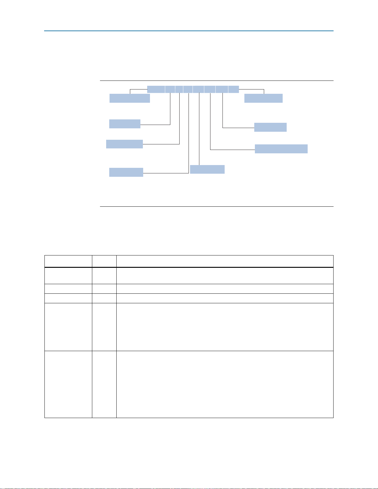
1–14 Chapter 1: Overview for the Arria II Device Family
Device Density
Pack ageTyp
e
3, 4, 5, or 6, with 3 being the fastest
Corresponds to pin count
17 = 358 pins
25 = 572 pins
29 = 780 pins
35 = 1152 pins
40 = 1517 pins
F: FineLine BGA (FBGA)
U: Ultra FineLine BGA (UBGA)
H: Hybrid FineLine BGA (HBGA)
GX: 45, 65, 95, 125, 190,260
GZ: 225, 300, 350
Optional SuffixFa m i l y S i g n a t u r e
Operat ing Tempe rature
Sp e e d Gr a d e
Ball Array Dimension
4
EP2AGX
45
C
17
F
N
Indicates specific device options
N: Lead-f ree devi ces
ES: Engineering sample
EP2AGX
EP2AGZ
C
Transceiver Count
C: 4
D: 8
E: 12
F:16
H: 24
C: Commercial temperature (t
J
= 0°C to 85°C)
I: Industrial temperature (t
J
= -40°C to 100°C)
Reference and Ordering Information
Reference and Ordering Information
Figure 1–3 shows the ordering codes for Arria II devices.
Figure 1–3. Packaging Ordering Information for Arria II Devices
Document Revision History
Tab le 1– 10 lists the revision history for this chapter.
Table 1–10. Document Revision History (Part 1 of 2)
Date Version Changes
July 2012 4.4
December 2011 4.3 Updated Table 1–4 and Table 1–9.
June 2011 4.2 Updated Table 1–2.
June 2011 4.1
December 2010 4.0
Arria II Device Handbook Volume 1: Device Interfaces and Integration July 2012 Altera Corporation
Replaced Table 1-10. External Memory Interface Maximum Performance for Arria II Devices
with link to the External Memory Interface Spec Estimator online tool.
■ Updated Figure 1–2.
■ Updated Table 1–10.
■ Updated the “Arria II Device Feature” section.
■ Added Table 1–6.
■ Minor text edits.
■ Updated for the Quartus II software version 10.0 release
■ Added information about Arria II GZ devices
■ Updated Table 1–1, Table 1–4, Table 1–5, Table 1–6, Table 1–7, and Table 1–9
■ Added Table 1–3
■ Added Figure 1–2
■ Updated Figure 1–3
■ Updated “Arria II Device Feature” and “Arria II Device Architecture” section
Page 29

Chapter 1: Overview for the Arria II Device Family 1–15
Document Revision History
Table 1–10. Document Revision History (Part 2 of 2)
Date Version Changes
Updated for the Quartus II software version 10.0 release:
■ Added information about –I3 speed grade
July 2010 3.0
November 2009 2.0
June 2009 1.1
■ Updated Table 1–1, Table 1–3, and Table 1–7
■ Updated Figure 1–2
■ Updated “Highlights” and “High-Speed LVDS I/O and DPA”section
■ Minor text edits
■ Updated Table 1–1, Table 1–2, and Table 1–3
■ Updated “Configuration Features” section
■ Updated Table 1–2.
■ Updated “I/O Features” section.
February 2009 1.0 Initial release.
July 2012 Altera Corporation Arria II Device Handbook Volume 1: Device Interfaces and Integration
Page 30

1–16 Chapter 1: Overview for the Arria II Device Family
Document Revision History
Arria II Device Handbook Volume 1: Device Interfaces and Integration July 2012 Altera Corporation
Page 31

Direct link
interconnect from
adjacent block
Direct link
interconnect to
adjacent block
Row Interconnects of
Variable Speed & Length
Column Interconnects of
Variable Speed & Length
Local Interconnect is Driven
from Either Side by Column Interconnect
& LABs, & from Above by Row Interconnect
Local Interconnect
LAB
Direct link
interconnect from
adjacent block
Direct link
interconnect to
adjacent block
ALMs
MLAB
C4 C12
R20
R4
December 2010
AIIGX51002-2.0
AIIGX51002-2.0
This chapter describes the features of the logic array block (LAB) in the Arria®II core
fabric. The LAB is composed of basic building blocks known as adaptive logic
modules (ALMs) that you can configure to implement logic functions, arithmetic
functions, and register functions.
This chapter contains the following sections:
■ “Logic Array Blocks” on page 2–1
■ “Adaptive Logic Modules” on page 2–5
Logic Array Blocks
Each LAB consists of ten ALMs, various carry chains, shared arithmetic chains, LAB
control signals, local interconnect, and register chain connection lines. The local
interconnect transfers signals between ALMs in the same LAB. The direct link
interconnect allows the LAB to drive into the local interconnect of its left and right
neighbors. Register chain connections transfer the output of the ALM register to the
adjacent ALM register in the LAB. The Quartus
the LAB or the adjacent LABs, allowing the use of local, shared arithmetic chain, and
register chain connections for performance and area efficiency.
2. Logic Array Blocks and Adaptive Logic Modules in Arria II Devices
®
II Compiler places associated logic in
Figure 2–1 shows the Arria II LAB structure and the LAB interconnects.
Figure 2–1. LAB Structure in Arria II Devices
© 2010 Altera Corporation. All rights reserved. ALTERA, ARRIA, CYCLONE, HARDCOPY, MAX, MEGACORE, NIOS, QUARTUS and STRATIX are Reg. U.S. Pat. & Tm. Off.
and/or trademarks of Altera Corporation in the U.S. and other countries. All other trademarks and service marks are the property of their respective holders as described at
www.altera.com/common/legal.html. Altera warrants performance of its semiconductor products to current specifications in accordance with Altera’s standard warranty, but
reserves the right to make changes to any products and services at any time without notice. Altera assumes no responsib ility or liability arising out of the application or use of any
information, product, or service described herein except as expressly agreed to in writing by Altera. Altera customers are advised to obtain the latest version of device
specifications before relying on any published information and before placing orders for products or services.
Arria II Device Handbook Volume 1: Device Interfaces and Integration
December 2010
Subscribe
Page 32

2–2 Chapter 2: Logic Array Blocks and Adaptive Logic Modules in Arria II Devices
MLAB
LAB
LUT-based-64 x 1
Simple dual port SRAM
LUT-based-64 x 1
Simple dual port SRAM
LUT-based-64 x 1
Simple dual port SRAM
LUT-based-64 x 1
Simple dual port SRAM
LUT-based-64 x 1
Simple dual port SRAM
LUT-based-64 x 1
Simple dual port SRAM
LUT-based-64 x 1
Simple dual port SRAM
LUT-based-64 x 1
Simple dual port SRAM
LUT-based-64 x 1
Simple dual port SRAM
LUT-based-64 x 1
Simple dual port SRAM
(1)
(1)
(1)
(1)
(1)
(1)
(1)
(1)
(1)
(1)
ALM
ALM
ALM
ALM
ALM
ALM
ALM
ALM
ALM
ALM
LAB Control Block LAB Control Block
Logic Array Blocks
The LAB of the Arria II device has a derivative called memory LAB (MLAB), which
adds look-up table (LUT)-based SRAM capability to the LAB. The MLAB supports a
maximum of 640 bits of simple dual-port SRAM. You can configure each ALM in an
MLAB as either a 64 × 1 or 32 × 2 block, resulting in a configuration of 64 × 10 or
32 × 20 simple dual-port SRAM blocks. MLAB and LAB blocks always coexist as pairs
in Arria II devices. MLAB is a superset of the LAB and includes all LAB features.
Figure 2–2 shows an overview of LAB and MLAB topology.
f For more information about MLABs, refer to the TriMatrix Memory Blocks in Arria II
Devices chapter.
Figure 2–2. LAB and MLAB Structure in Arria II Devices
Note to Figure 2–2:
(1) You can use an MLAB ALM as a regular LAB ALM or configure it as a dual-port SRAM.
Arria II Device Handbook Volume 1: Device Interfaces and Integration December 2010 Altera Corporation
Page 33

Chapter 2: Logic Array Blocks and Adaptive Logic Modules in Arria II Devices 2–3
ALMs
Direct link
interconnect
to right
Direct link interconnect from
right LAB, memory block,
DSP block, or IOE output
Direct link interconnect from
left LAB, memory block,
DSP block, or IOE output
Local
Interconnect
LAB
ALMs
Direct link
interconnect
to left
MLAB
Logic Array Blocks
LAB Interconnects
The LAB local interconnect drives the ALMs in the same LAB using column and row
interconnects and the ALM outputs in the same LAB. The direct link connection
feature minimizes the use of row and column interconnects, providing higher
performance and flexibility. Adjacent LABs/MLABs, memory blocks, or DSP blocks
from the left or right can also drive the LAB’s local interconnect through the direct
link connection. Each LAB can drive 30 ALMs through fast local and direct link
interconnects. Ten ALMs are in any given LAB and ten ALMs are in each of the
adjacent LABs.
Figure 2–3 shows the direct link connection, which connects adjacent LABs, memory
blocks, DSP blocks, or I/O element (IOE) outputs.
Figure 2–3. Direct Link Connection
December 2010 Altera Corporation Arria II Device Handbook Volume 1: Device Interfaces and Integration
Page 34

2–4 Chapter 2: Logic Array Blocks and Adaptive Logic Modules in Arria II Devices
Dedicated Row LAB Clocks
Local Interconnect
Local Interconnect
Local Interconnect
Local Interconnect
Local Interconnect
Local Interconnect
labclk2
syncload
labclkena0
or asyncload
or labpreset
labclk0
labclk1
labclr1
labclkena1 labclkena2 labclr0 synclr
6
6
6
There are two unique
clock signals per LAB.
Logic Array Blocks
LAB Control Signals
Each LAB contains dedicated logic for driving a maximum of 10 control signals to its
ALMs at a time. Control signals include three clocks, three clock enables, two
asynchronous clears, a synchronous clear, and synchronous load control signals.
Although you generally use synchronous-load and clear signals when implementing
counters, you can also use them with other functions. Each LAB has two unique clock
sources and three clock enable signals, as shown in Figure 2–4. The LAB control block
can generate up to three clocks using two clock sources and three clock enable signals.
Each clock and clock enable signals are linked. For example, any ALM in a particular
LAB using the
the rising and falling edges of a clock, it also uses two LAB-wide clock signals.
De-asserting the clock enable signal turns off the corresponding LAB-wide clock. The
LAB row clocks [5..0] and LAB local interconnects generate the LAB-wide control
signals. In addition to data, the inherent low skew of the MultiTrack interconnect
allows clock and control signal distribution.
Figure 2–4. LAB-Wide Control Signals
labclk1
signal also uses the
labclkena1
signal. If the LAB uses both
Arria II Device Handbook Volume 1: Device Interfaces and Integration December 2010 Altera Corporation
Page 35

Chapter 2: Logic Array Blocks and Adaptive Logic Modules in Arria II Devices 2–5
DQ
To general or
local routing
reg0
To general or
local routing
datae0
dataf0
reg_chain_in
reg_chain_out
adder0
dataa
datab
datac
datad
datae1
dataf1
DQ
To general or
local routing
reg1
To general or
local routing
adder1
carry_in
carry_out
Combinational/Memory ALUT0
6-Input LUT
6-Input LUT
shared_arith_out
shared_arith_in
Combinational/Memory ALUT1
labclk
Adaptive Logic Modules
Adaptive Logic Modules
The ALM is the basic building block of logic in the Arria II device architecture. Each
ALM contains a variety of LUT-based resources that can be divided between two
combinational adaptive LUTs (ALUTs) and two registers. With up to eight inputs for
the two combinational ALUTs, one ALM can implement various combinations of two
functions. This adaptability allows an ALM to be completely backward-compatible
with 4-input LUT architectures. One ALM can also implement any function with up
to 6-input and certain 7-input functions. In addition to the ALUT-based resources,
each ALM contains two programmable registers, two dedicated full adders, a carry
chain, a shared arithmetic chain, and a register chain. Through these dedicated
resources, an ALM can efficiently implement various arithmetic functions and shift
registers. Each ALM drives all types of interconnects: local, row, column, carry chain,
shared arithmetic chain, register chain, and direct link. Figure 2–5 shows a high-level
block diagram of the Arria II ALM.
Figure 2–5. High-Level Block Diagram of the Arria II ALM
December 2010 Altera Corporation Arria II Device Handbook Volume 1: Device Interfaces and Integration
Page 36

2–6 Chapter 2: Logic Array Blocks and Adaptive Logic Modules in Arria II Devices
D Q
+
reg_chain_in
aclr[1:0]
sclr
syncload
clk[2:0]
carry_in
dataf0
datae0
dataa
datab
datac1
datae1
dataf1
shared_arith_out
carry_out
reg_chain_out
CLR
D Q
CLR
shared_arith_in
local
interconnect
row, column
direct link routing
row, column
direct link routing
local
interconnect
4-INPUT
LUT
4-INPUT
LUT
3-INPUT
LUT
3-INPUT
LUT
3-INPUT
LUT
3-INPUT
LUT
+
datac0
V
CC
GND
row, column
direct link routing
row, column
direct link routing
Adaptive Logic Modules
Figure 2–6 shows a detailed view of all the connections in an ALM.
Figure 2–6. Connection Details of the Arria II ALM
One ALM contains two programmable registers. Each register has data, clock, clock
enable, synchronous and asynchronous clear, and synchronous load and clear inputs.
Global signals, general purpose I/O (GPIO) pins, or any internal logic can drive the
register’s clock and clear-control signals. Either GPIO pins or internal logic can drive
the clock enable. For combinational functions, the register is bypassed and the output
of the LUT drives directly to the outputs of an ALM.
Each ALM has two sets of outputs that drive the local, row, and column routing
resources. The LUT, adder, or register output can drive the ALM outputs (refer to
Figure 2–6). For each set of output drivers, two ALM outputs can drive column, row,
or direct link routing connections, and one of these ALM outputs can also drive local
interconnect resources. The LUT or adder can drive one output while the register
drives another output.
Arria II Device Handbook Volume 1: Device Interfaces and Integration December 2010 Altera Corporation
Page 37

Chapter 2: Logic Array Blocks and Adaptive Logic Modules in Arria II Devices 2–7
Adaptive Logic Modules
This feature is called register packing. It improves device utilization by allowing the
device to use the register and combinational logic for unrelated functions. Another
mechanism to improve fitting is to allow the register output to feed back into the LUT
of the same ALM so that the register is packed with its own fan-out LUT. The ALM
can also drive out registered and unregistered versions of the LUT or adder output.
The Quartus II software automatically configures the ALMs for optimized
performance.
ALM Operating Modes
The Arria II ALM can operate in any of the following modes:
■ Normal
■ Extended LUT
■ Arithmetic
■ Shared Arithmetic
■ LUT-Register
The Quartus II software and other supported third-party synthesis tools, in
conjunction with parameterized functions such as the library of parameterized
modules (LPM) functions, automatically choose the appropriate mode for common
functions such as counters, adders, subtractors, and arithmetic functions. Each mode
uses the ALM resources differently. In each mode, eleven available inputs to an
ALM—the eight data inputs from the LAB local interconnect, carry-in from the
previous ALM or LAB, the shared arithmetic chain connection from the previous
ALM or LAB, and the register chain connection—are directed to different destinations
to implement the desired logic function. LAB-wide signals provide clock,
asynchronous clear, synchronous clear, synchronous load, and clock enable control for
the register. These LAB-wide signals are available in all ALM modes. For more
information on the LAB-wide control signals, refer to “LAB Control Signals” on
page 2–4.
December 2010 Altera Corporation Arria II Device Handbook Volume 1: Device Interfaces and Integration
Page 38

2–8 Chapter 2: Logic Array Blocks and Adaptive Logic Modules in Arria II Devices
6-Input
LUT
dataf0
datae0
dataf0
datae0
dataa
datab
dataa
datab
datab
datac
datac
dataf0
datae0
dataa
datac
6-Input
LUT
datad
datad
datae1
combout0
combout1
combout0
combout1
combout0
combout1
dataf1
datae1
dataf1
datad
datae1
dataf1
4-Input
LUT
4-Input
LUT
4-Input
LUT
6-Input
LUT
dataf0
datae0
dataa
datab
datac
datad
combout0
5-Input
LUT
5-Input
LUT
dataf0
datae0
dataa
datab
datac
datad
combout0
combout1
datae1
dataf1
5-Input
LUT
dataf0
datae0
dataa
datab
datac
datad
combout0
combout1
datae1
dataf1
5-Input
LUT
3-Input
LUT
Adaptive Logic Modules
Normal Mode
Normal mode is suitable for general logic applications and combinational functions.
In this mode, up to eight data inputs from the LAB local interconnect are inputs to the
combinational logic. Normal mode allows two functions to be implemented in one
Arria II ALM, or a single function of up to six inputs. The ALM can support certain
combinations of completely independent functions and various combinations of
functions that have common inputs.
Figure 2–7 shows the supported LUT combinations in normal mode.
Figure 2–7. ALM in Normal Mode (Note 1)
Note to Figure 2–7:
(1) Combinations of functions with fewer inputs than those shown are also supported. For example, combinations of functions with the following
number of inputs are supported: 4 and 3, 3 and 3, 3 and 2, and 5 and 2.
Normal mode provides complete backward-compatibility with 4-input LUT
architectures.
Arria II Device Handbook Volume 1: Device Interfaces and Integration December 2010 Altera Corporation
Page 39

Chapter 2: Logic Array Blocks and Adaptive Logic Modules in Arria II Devices 2–9
6-Input
LUT
dataf0
datae0
dataa
datab
datac
datad
datae1
dataf1
DQ
DQ
To general or
local routing
To general or
local routing
To general or
local routing
reg0
reg1
(2)
labclk
Adaptive Logic Modules
For the packing of two 5-input functions into one ALM, the functions must have at
least two common inputs. The common inputs are
of a 4-input function with a 5-input function requires one common input (either
or
datab
).
dataa
and
datab
. The combination
dataa
In the case of implementing two 6-input functions in one ALM, four inputs must be
shared and the combinational function must be the same. In a sparsely used device,
functions that could be placed in one ALM may be implemented in separate ALMs by
the Quartus II software to achieve the best possible performance. As a device begins
to fill up, the Quartus II software automatically utilizes the full potential of the
Arria II ALM. The Quartus II Compiler automatically searches for functions using
common inputs or completely independent functions to be placed in one ALM to
make efficient use of device resources. In addition, you can manually control resource
usage by setting location assignments.
Any 6-input function can be implemented using inputs
and either
the output is driven to
datae0
and
dataf0
or
register0
datae1
, and/or
and
dataf1
register0
dataa, datab, datac, datad
. If
datae0
and
dataf0
is bypassed and the data drives
out to the interconnect using the top set of output drivers (refer to Figure 2–8). If
datae1
register1
and
dataf1
are used, the output either drives to
register1
or bypasses
and drives to the interconnect using the bottom set of output drivers. The
Quartus II Compiler automatically selects the inputs to the LUT. ALMs in normal
mode support register packing.
Figure 2–8. Input Function in Normal Mode (Note 1)
Notes to Figure 2–8:
(1) If datae1 and dataf1 are used as inputs to a 6-input function, datae0 and dataf0 are available for register packing.
(2) The dataf1 input is available for register packing only if the 6-input function is unregistered.
,
are utilized,
December 2010 Altera Corporation Arria II Device Handbook Volume 1: Device Interfaces and Integration
Page 40

2–10 Chapter 2: Logic Array Blocks and Adaptive Logic Modules in Arria II Devices
Adaptive Logic Modules
Extended LUT Mode
Use extended LUT mode to implement a specific set of 7-input functions. The set must
be a 2-to-1 multiplexer fed by two arbitrary 5-input functions sharing four inputs.
Figure 2–9 shows the template of supported 7-input functions using extended LUT
mode. In this mode, if the 7-input function is unregistered, the unused eighth input is
available for register packing.
Functions that fit into the template, as shown in Figure 2–9, often appear in designs as
“if-else” statements in Verilog HDL or VHDL code.
Figure 2–9. Template for Supported 7-Input Functions in Extended LUT Mode
datae0
datac
dataa
datab
datad
dataf0
datae1
5-Input
LUT
5-Input
LUT
combout0
DQ
reg0
To general or
local routing
To general or
local routing
dataf1
(1)
This input is available
for register packing.
Note to Figure 2–9:
(1) If the 7-input function is unregistered, the unused eighth input is available for register packing. The second register, reg1, is not available.
Arria II Device Handbook Volume 1: Device Interfaces and Integration December 2010 Altera Corporation
Page 41

Chapter 2: Logic Array Blocks and Adaptive Logic Modules in Arria II Devices 2–11
datae0
carry_in
carry_out
dataa
datab
datac
datad
datae1
DQ
DQ
To general or
local routing
To general or
local routing
reg0
reg1
To general or
local routing
To general or
local routing
4-Input
LUT
4-Input
LUT
4-Input
LUT
4-Input
LUT
adder1
adder0
dataf0
dataf1
Adaptive Logic Modules
Arithmetic Mode
Arithmetic mode is ideal for implementing adders, counters, accumulators, wide
parity functions, and comparators. The ALM in arithmetic mode uses two sets of two
4-input LUTs along with two dedicated full adders. The dedicated adders allow the
LUTs to be available to perform pre-adder logic; therefore, each adder can add the
output of two 4-input functions. The four LUTs share
shown in Figure 2–10, the carry-in signal feeds to
adder0
feeds to the carry-in of
the next ALM in the LAB. ALMs in arithmetic mode can drive out registered and
unregistered versions of the adder outputs.
Figure 2–10. ALM in Arithmetic Mode
adder1
. The carry-out from
dataa
adder0
and
datab
inputs. As
and the carry-out from
adder1
drives to
adder0
of
In arithmetic mode, the ALM supports simultaneous use of the adder’s carry output
along with combinational logic outputs. The adder output is ignored in this operation.
Using the adder with combinational logic output provides resource savings of up to
50% for functions that can use this mode.
Arithmetic mode also offers clock enable, counter enable, synchronous up and down
control, add and subtract control, synchronous clear, and synchronous load. The LAB
local interconnect data inputs generate the clock enable, counter enable, synchronous
up and down, and add and subtract control signals. These control signals are good
candidates for the inputs that share the four LUTs in the ALM. The synchronous clear
December 2010 Altera Corporation Arria II Device Handbook Volume 1: Device Interfaces and Integration
and synchronous load options are LAB-wide signals that affect all registers in the
LAB. These signals can also be individually disabled or enabled per register. The
Quartus II software automatically places any registers that are not used by the counter
into other LABs.
Page 42

2–12 Chapter 2: Logic Array Blocks and Adaptive Logic Modules in Arria II Devices
Adaptive Logic Modules
Carry Chain
The carry chain provides a fast carry function between the dedicated adders in
arithmetic or shared arithmetic mode. The two-bit carry select feature in Arria II
devices halves the propagation delay of carry chains within the ALM. Carry chains
can begin in either the first ALM or the fifth ALM in a LAB. The final carry-out signal
is routed to an ALM, where it is fed to local, row, or column interconnects.
The Quartus II Compiler automatically creates carry chain logic during design
processing, or you can create it manually during design entry. Parameterized
functions such as LPM automatically take advantage of carry chains for the
appropriate functions.
The Quartus II Compiler creates carry chains longer than 20 ALMs (10 ALMs in
arithmetic or shared arithmetic mode) by linking LABs together automatically. To
enhance fitting, a long carry chain runs vertically, allowing fast horizontal connections
to TriMatrix memory and DSP blocks. A carry chain can continue as far as a full
column.
To avoid routing congestion in one small area of the device when a high fan-in
arithmetic function is implemented, the LAB can support carry chains that only use
either the top half or bottom half of the LAB before connecting to the next LAB. This
leaves the other half of the ALMs in the LAB available for implementing narrower
fan-in functions in normal mode. Carry chains that use the top five ALMs in the first
LAB carry into the top half of the ALMs in the next LAB in the column. Carry chains
that use the bottom five ALMs in the first LAB carry into the bottom half of the ALMs
in the next LAB within the column. In every alternate LAB column, the top half can be
bypassed; in the other MLAB columns, the bottom half can be bypassed.
1 For more information on carry chain interconnect, refer to “ALM Interconnects” on
page 2–17.
Arria II Device Handbook Volume 1: Device Interfaces and Integration December 2010 Altera Corporation
Page 43

Chapter 2: Logic Array Blocks and Adaptive Logic Modules in Arria II Devices 2–13
datae0
carry_in
shared_arith_in
shared_arith_out
carry_out
dataa
datab
datac
datad
datae1
DQ
DQ
To general or
local routing
To general or
local routing
reg0
reg1
To general or
local routing
To general or
local routing
4-Input
LUT
4-Input
LUT
4-Input
LUT
4-Input
LUT
labclk
Adaptive Logic Modules
Shared Arithmetic Mode
In shared arithmetic mode, the ALM can implement a 3-input add in an ALM. In this
mode, the ALM is configured with four 4-input LUTs. Each LUT either computes the
sum of three inputs or the carry of three inputs. The output of the carry computation
is fed to the next adder using a dedicated connection called the shared arithmetic
chain. This shared arithmetic chain can significantly improve the performance of an
adder tree by reducing the number of summation stages required to implement an
adder tree. Figure 2–11 shows the ALM using this feature.
Figure 2–11. ALM in Shared Arithmetic Mode
You can find adder trees in many different applications. For example, the summation
of the partial products in a logic-based multiplier can be implemented in a tree
structure. Another example is a correlator function that can use a large adder tree to
sum filtered data samples in a given time frame to recover or de-spread data that was
December 2010 Altera Corporation Arria II Device Handbook Volume 1: Device Interfaces and Integration
transmitted using spread-spectrum technology.
Page 44

2–14 Chapter 2: Logic Array Blocks and Adaptive Logic Modules in Arria II Devices
Adaptive Logic Modules
Shared Arithmetic Chain
The shared arithmetic chain available in enhanced arithmetic mode allows the ALM
to implement a 3-input add. This significantly reduces the resources necessary to
implement large adder trees or correlator functions.
The shared arithmetic chains can begin in either the first or sixth ALM in an LAB. The
Quartus II Compiler creates shared arithmetic chains longer than 20 ALMs (10 ALMs
in arithmetic or shared arithmetic mode) by linking LABs together automatically. To
enhance fitting, a long shared arithmetic chain runs vertically, allowing fast horizontal
connections to the TriMatrix memory and DSP blocks. A shared arithmetic chain can
continue as far as a full column.
Similar to the carry chains, the top and bottom half of shared arithmetic chains in
alternate LAB columns can be bypassed. This capability allows the shared arithmetic
chain to cascade through half of the ALMs in an LAB while leaving the other half
available for narrower fan-in functionality. Every other LAB column is top-half
bypassable, while the other LAB columns are bottom-half bypassable.
1 For more information on shared arithmetic chain interconnect, refer to “ALM
Interconnects” on page 2–17.
Arria II Device Handbook Volume 1: Device Interfaces and Integration December 2010 Altera Corporation
Page 45

Chapter 2: Logic Array Blocks and Adaptive Logic Modules in Arria II Devices 2–15
4-input
LUT
5-input
LUT
clk
aclr
datain(datac)
sclr
sumout
Master latch
Slave latch
combout
LUT regout
sumout
combout
Adaptive Logic Modules
LUT-Register Mode
LUT-Register mode allows third register capability in an ALM. Two internal feedback
loops allow combinational
ALUT0
to implement the slave latch needed for the third register. The LUT register
shares its clock, clock enable, and asynchronous clear sources with the top dedicated
register. Figure 2–12 shows the register constructed using two combinational blocks in
the ALM.
Figure 2–12. LUT Register from Two Combinational Blocks
ALUT1
to implement the master latch and combinational
Figure 2–13 shows the ALM in LUT-Register mode.
Figure 2–13. ALM in LUT-Register Mode with 3-Register Capability
clk [2..0]
aclr [1..0] reg_chain_in
Third register
DC1
E0
F1
E1
F0
datain
aclr
sclr
regout
latchout
datain
sdata
datain
sdata
aclr
aclr
regout
regout
lelocal 0
leout 0 a
leout 0 b
lelocal 1
leout 1 a
leout 1 b
reg_chain_out
December 2010 Altera Corporation Arria II Device Handbook Volume 1: Device Interfaces and Integration
Page 46

2–16 Chapter 2: Logic Array Blocks and Adaptive Logic Modules in Arria II Devices
Adaptive Logic Modules
Register Chain
In addition to general routing outputs, the ALMs in any given LAB have register
chain outputs to allow registers in the same LAB to be cascaded together. The register
chain interconnect allows a LAB to use LUTs for a single combinational function and
the registers to be used for an unrelated shift register implementation. These resources
speed up connections between ALMs while saving local interconnect resources (refer
to Figure 2–14). The Quartus II Compiler automatically takes advantage of these
resources to improve utilization and performance.
Figure 2–14. Register Chain in an LAB (Note 1)
From previous ALM
labclk
in the LAB
DQ
reg0
To general or
local routing
To general or
local routing
reg_chain_in
adder0
Combinational
Logic
To general or
local routing
To general or
local routing
To general or
local routing
To general or
local routing
To general or
local routing
To general or
local routing
Combinational
Logic
adder1
adder0
adder1
DQ
reg1
DQ
reg0
DQ
reg1
reg_chain_out
To next ALM
in the LAB
Note to Figure 2–14:
(1) You can use the combinational or adder logic to implement an unrelated, un-registered function.
1 For more information about register chain interconnect, refer to “ALM Interconnects”
on page 2–17.
Arria II Device Handbook Volume 1: Device Interfaces and Integration December 2010 Altera Corporation
Page 47

Chapter 2: Logic Array Blocks and Adaptive Logic Modules in Arria II Devices 2–17
t
Adaptive Logic Modules
ALM Interconnects
There are three dedicated paths between ALMs: Register Cascade, Carry-chain, and
Shared Arithmetic chain. Arria II devices include an enhanced interconnect structure
in LABs for routing shared arithmetic chains and carry chains for efficient arithmetic
functions. The register chain connection allows the register output of one ALM to
connect directly to the register input of the next ALM in the LAB for fast shift
registers. These ALM-to-ALM connections bypass the local interconnect. Figure 2–15
shows the shared arithmetic chain, carry chain, and register chain interconnects.
Figure 2–15. Shared Arithmetic Chain, Carry Chain, and Register Chain Interconnects
Local interconnect
routing among ALMs
in the LAB
Carry chain & shared
arithmetic chain
routing to adjacent ALM
Local
interconnect
Clear and Preset Logic Control
LAB-wide signals control the logic for the register‘s clear signal. The ALM directly
supports an asynchronous clear function. You can achieve the register preset through
the Quartus II software’s NOT-gate push-back logic option. Each LAB supports up to
two clears.
Arria II devices provide a device-wide reset pin (
the device. An option set before compilation in the Quartus II software enables this
pin. This device-wide reset overrides all other control signals.
LAB Power Management Techniques
...
ALM 1
ALM 2
ALM 3
...
ALM 10
DEV_CLRn
Register chain
routing to adjacent
ALM's register inpu
) that resets all registers in
The following techniques are used to manage static and dynamic power consumption
within the LAB:
■ The Quartus II software forces all adder inputs low when ALM adders are not in
use to save AC power.
■ Arria II LABs operate in high-performance mode or low-power mode. The
Quartus II software automatically chooses the appropriate mode for the LAB,
based on the design, to optimize speed versus leakage trade-offs.
December 2010 Altera Corporation Arria II Device Handbook Volume 1: Device Interfaces and Integration
Page 48

2–18 Chapter 2: Logic Array Blocks and Adaptive Logic Modules in Arria II Devices
■ Clocks represent a significant portion of dynamic power consumption due to their
Document Revision History
high switching activity and long paths. The LAB clock that distributes a clock
signal to registers within an LAB is a significant contributor to overall clock power
consumption. Each LAB’s clock and clock enable signal are linked. For example, a
combinational ALUT or register in a particular LAB using the
uses the
labclkena1
signal. To disable an LAB-wide clock power consumption
labclk1
signal also
without disabling the entire clock tree, use the LAB-wide clock enable to gate the
LAB-wide clock. The Quartus II software automatically promotes register-level
clock enable signals to the LAB-level. All registers within the LAB that share a
common clock and clock enable are controlled by a shared, gated clock. To take
advantage of these clock enables, use a clock-enable construct in your HDL code
for the registered logic.
f For more information about implementing static and dynamic power consumption
within the LAB, refer to the Power Optimization chapter in volume 2 of the Quartus II
Handbook.
Document Revision History
Tab le 2– 1 lists the revision history for this document.
Table 2–1. Document Revision History
Date Version Changes
Updated for the Quartus II software version 10.1 release:
■ Added Arria II GZ device information.
December 2010 2.0
■ Updated “Logic Array Blocks”, “LAB Interconnects”, “LAB Control Signals”, “Adaptive
Logic Modules”, “ALM Operating Modes”, “Normal Mode” sections.
■ Added Figure 2–7 and Figure 2–8.
■ Added “LAB Power Management Techniques” section.
June 2009 1.1 Updated Figure 2–6.
February 2009 1.0 Initial Release.
Arria II Device Handbook Volume 1: Device Interfaces and Integration December 2010 Altera Corporation
Page 49

December 2011
AIIGX51003-3.2
AIIGX51003-3.2
3. Memory Blocks in Arria II Devices
This chapter describes the Arria® II device memory blocks that include 640-bit
memory logic array blocks (MLABs), 9-Kbit M9K blocks, and 144-Kbit M144K blocks.
MLABs are optimized to implement filter delay lines, small FIFO buffers, and shift
registers. You can use the M9K blocks for general purpose memory applications and
the M144K blocks for processor code storage, packet buffering, and video frame
buffering.
1 M144K block is only available for Arria II GZ devices.
You can configure each embedded memory block independently with the Quartus
MegaWizard
™
Plug-In Manager to be a single- or dual-port RAM, FIFO, ROM, or shift
register. You can stitch together multiple blocks of the same type to produce larger
memories with a minimal timing penalty.
This chapter contains the following sections:
■ “Memory Features” on page 3–2
■ “Memory Modes” on page 3–10
■ “Clocking Modes” on page 3–19
■ “Design Considerations” on page 3–20
®
II
© 2011 Altera Corporation. All rights reserved. ALTERA, ARRIA, CYCLONE, HARDCOPY, MAX, MEGACORE, NIOS, QUARTUS and STRATIX are Reg. U.S. Pat. & Tm. Off.
and/or trademarks of Altera Corporation in the U.S. and other countries. All other trademarks and service marks are the property of their respective holders as described at
www.altera.com/common/legal.html. Altera warrants performance of its semiconductor products to current specifications in accordance with Altera’s standard warranty, but
reserves the right to make changes to any products and services at any time without notice. Altera assumes no responsib ility or liability arising out of the application or use of any
information, product, or service described herein except as expressly agreed to in writing by Altera. Altera customers are advised to obtain the latest version of device
specifications before relying on any published information and before placing orders for products or services.
Arria II Device Handbook Volume 1: Device Interfaces and Integration
December 2011
Subscribe
Page 50

3–2 Chapter 3: Memory Blocks in Arria II Devices
Memory Features
Memory Features
Tab le 3– 1 lists the features supported by the embedded memory blocks.
Table 3–1. Summary of Memory Features in Arria II Devices (Part 1 of 2)
Feature
Maximum performance 500 MHz 500 MHz 390 MHz 540 MHz 500 MHz
Total RAM bits (including parity
bits)
Configurations (depth × width)
Parity bits vvvv v
Byte enable vvvv v
Packed mode — — vv v
Address clock enable vvvv v
Single-port memory vvvv v
Simple dual-port memory vvvv v
True dual-port memory — — vv v
Embedded shift register vvvv v
ROM vvvv v
FIFO buffer vvvv v
Simple dual-port mixed width
support
True dual-port mixed width
support
Memory initialization file (.mif) vvvv v
Mixed-clock mode vvvv v
Power-up condition
Register clears Output registers Output registers Output registers
Write/Read operation triggering
Same-port read-during-write
Arria II GX Arria II GZ Arria II GX Arria II GZ Arria II GZ
64 × 10
32 × 16
32 × 18
32 × 20
Outputs cleared if registered,
otherwise reads memory
Write: Falling clock edges.
Read: Rising clock edges
Outputs set to
old data
MLABs M9K Blocks M144K Blocks
640 640 9,216 9,216 147,456
edges
8K × 1
4K × 2
2K × 4
1K × 8
1K × 9
512 × 16
512 × 18
256 × 32
256 × 36
16K × 8
16K × 9
8K × 16
8K × 18
4K × 32
4K × 36
2K × 64
2K × 72
Write and Read: Rising
clock edges
Outputs set to old data or
new data
8K × 1
64×8
64×9
——vv v
——vv v
contents.
64 × 8
64 × 9
64 × 10
32 × 16
32 × 18
32 × 20
Outputs set
to don’t care
4K × 2
2K × 4
1K × 8
1K × 9
512 × 16
512 × 18
256 × 32
256 × 36
Outputs cleared Outputs cleared
Write and Read: Rising clock
Outputs set to old data or
new data
Arria II Device Handbook Volume 1: Device Interfaces and Integration December 2011 Altera Corporation
Page 51

Chapter 3: Memory Blocks in Arria II Devices 3–3
Memory Features
Table 3–1. Summary of Memory Features in Arria II Devices (Part 2 of 2)
Feature
Mixed-port read-during-write
ECC Support
Arria II GX Arria II GZ Arria II GX Arria II GZ Arria II GZ
Outputs set to old data,
Soft IP support using the
MLABs M9K Blocks M144K Blocks
new data, or
don’t care
Quartus II software
Outputs set to old data or
don’t care
Soft IP support using the
Quartus II software
Built-in support in
×64-wide simple dual-port
mode or soft IP support
using the Quartus II
Tab le 3– 2 lists the capacity and distribution of the memory blocks in each Arria II
device.
Table 3–2. Memory Capacity and Distribution in Arria II Devices
Device MLABs M9K Blocks M144K Total RAM Bits (including MLABs) (Kbits)
EP2AGX45 903 319 — 3,435
EP2AGX65 1,265 495 — 5,246
EP2AGX95 1,874 612 — 6,679
EP2AGX125 2,482 730 — 8,121
EP2AGX190 3,806 840 — 9,939
EP2AGX260 5,130 950 — 11,756
EP2AGZ225 4,480 1,235 — 13,915
EP2AGZ300 5,960 1,248 24 18,413
EP2AGZ350 6,970 1,248 36 20,772
Outputs set to
old data or
don’t care
software
Memory Block Types
M9K and M144K memory blocks are dedicated resources. MLABs are dual-purpose
blocks. You can configure the MLABs as regular logic array blocks (LABs) or as
MLABs. Ten ALMs make up one MLAB. You can configure each ALM in an MLAB as
either a 64 × 1 or a 32 × 2 block, resulting in a 64 × 10 or 32 × 20 simple dual-port
SRAM block in a single MLAB.
Parity Bit Support
All memory blocks have built-in parity bit support. The ninth bit associated with each
byte can store a parity bit or serve as an additional data bit. No parity function is
actually performed on the ninth bit.
Byte Enable Support
All memory blocks support byte enables that mask the input data so that only specific
bytes of data are written. The unwritten bytes retain the previous written value. The
write enable (
write operations of the RAM blocks.
December 2011 Altera Corporation Arria II Device Handbook Volume 1: Device Interfaces and Integration
wren
) signals, along with the byte enable (
byteena
) signals, control the
Page 52

3–4 Chapter 3: Memory Blocks in Arria II Devices
inclock
wren
address
data
don't care: q (asynch)
byteena
XXXX
ABCD XXXX
XX
10 01
11
XX
an
a0 a1 a2 a0 a1 a2
ABCDFFFF
FFFF ABFF
FFFF FFCD
contents at a0
contents at a1
contents at a2
doutn
ABXX
XXCD
ABCD ABFF FFCD
ABCD
doutn
ABFF
FFCD
ABCD ABFF FFCD
ABCD
current data: q (asynch)
Memory Features
The default value for the byte enable signals is high (enabled), in which case writing is
controlled only by the write enable signals. The byte enable registers have no clear
port. When using parity bits on the M9K and M144K blocks, the byte enable controls
all 9 bits (8 bits of data plus 1 parity bit). When using parity bits on the MLAB, the
byte-enable controls all 10 bits in the widest mode.
Byte enables are only supported for true dual-port memory configurations when both
the PortA and PortB data widths of the individual M9K memory blocks are multiples
of 8 or 9 bits. For example, you cannot use byte enable for a mixed data width
memory configured with portA=32 and portB=8 because the mixed data width
memory is implemented as 2 separate 16 x 4 bit memories.
Byte enables operate in a one-hot fashion, with the LSB of the
corresponding to the LSB of the data bus. For example, if you use a RAM block in ×18
mode,
byteena = 11
byteena = 01, data[8..0]
, both
data[8..0]
and
is enabled and
data[17..9]
high.
1 You cannot use the byte enable feature when using the error correction coding (ECC)
feature on M144K blocks.
Figure 3–1 shows how the write enable (
control the operations of the M9K and M144K memory blocks.
When a byte-enable bit is deasserted during a write cycle, the corresponding data byte
output can appear as either a “don’t care” value or the current data at that location.
The output value for the masked byte is controllable using the Quartus II software.
When a byte-enable bit is asserted during a write cycle, the corresponding data byte
output also depends on the setting chosen in the Quartus II software.
Figure 3–1. Byte Enable Functional Waveform for M9K and M144K
data[17..9]
are enabled. Byte enables are active
wren
) and byte enable (
byteena
signal
is disabled. Similarly, if
byteena
) signals
Arria II Device Handbook Volume 1: Device Interfaces and Integration December 2011 Altera Corporation
Page 53

Chapter 3: Memory Blocks in Arria II Devices 3–5
inclock
wren
address
data
byteena
XXXX
ABCD XXXX
ABCDFFFF
FFFF ABFF
FFFF FFCD
contents at a0
contents at a1
contents at a2
current data: q (asynch)
doutn
FFFF
FFCD
ABCD
FFFF
ABFF FFCD FFCD
an a0 a1 a2 a0 a1 a2
XX 10 01 11 XX
ABFF
FFFF
Memory Features
Figure 3–2 shows how the
wren
MLABs. Falling clock edges triggers the write operation in MLABs.
Figure 3–2. Byte Enable Functional Waveform for MLABs
and
byteena
signals control the operations of the
Packed Mode Support
Arria II M9K and M144K blocks support packed mode. The packed mode feature
packs two independent single-port RAMs into one memory block. The Quartus II
software automatically implements the packed mode where appropriate by placing
the physical RAM block into true dual-port mode and using the MSB of the address to
distinguish between the two logical RAMs. The size of each independent single-port
RAM must not exceed half of the target block size.
Address Clock Enable Support
Arria II memory blocks support address clock enable, which holds the previous
address value for as long as the signal is enabled (
configure the memory blocks in dual-port mode, each port has its own independent
address clock enable. The default value for the address clock enable signal is low
(disabled).
addressstall
= 1). When you
December 2011 Altera Corporation Arria II Device Handbook Volume 1: Device Interfaces and Integration
Page 54

3–6 Chapter 3: Memory Blocks in Arria II Devices
address[0]
address[N]
addressstall
clock
1
0
address[0]
register
address[N]
register
address[N]
address[0]
1
0
Memory Features
Figure 3–3 shows an address clock enable block diagram. The port name
addressstall
refers to the address clock enable.
Figure 3–3. Address Clock Enable
Figure 3–4 shows the address clock enable waveform during the read cycle.
Figure 3–4. Address Clock Enable During Read Cycle Waveform
inclock
rdaddress
rden
addressstall
latched address
(inside memory)
q (synch)
q (asynch)
an a0
doutn-1
doutn
a0 a1 a2 a3 a4 a5
doutn
dout0
dout0
a1
dout1
dout1
a4
dout4
a6
a5
dout4
dout5
Arria II Device Handbook Volume 1: Device Interfaces and Integration December 2011 Altera Corporation
Page 55

Chapter 3: Memory Blocks in Arria II Devices 3–7
Memory Features
Figure 3–5 shows the address clock enable waveform during write cycle for M9K and
M144K blocks.
Figure 3–5. Address Clock Enable During Write Cycle Waveform for M9K and M144K Blocks
inclock
wraddress
data
wren
addressstall
latched address
(inside memory)
contents at a0
contents at a1
a0 a1 a2 a3 a4 a5
XX
01 02
01
03 04
a1
00
02
00
an a0
XX
05
a4 a5
03
a6
06
contents at a2
contents at a3
contents at a4
contents at a5
XX
XX
XX
XX
Figure 3–6 shows the address clock enable waveform during the write cycle for
MLABs.
Figure 3–6. Address Clock Enable During Write Cycle Waveform for MLABs
inclock
wraddress
data
wren
addressstall
latched address
(inside memory)
contents at a0
contents at a1
contents at a2
a0
00
an
XX
a1 a2 a3 a4 a5
a0
XX
01 02
01
03
a1
02
XX
00
04
a4 a5
03
05
04
05
a6
06
contents at a3
contents at a4
contents at a5
December 2011 Altera Corporation Arria II Device Handbook Volume 1: Device Interfaces and Integration
XX
XX
XX
04
05
Page 56

3–8 Chapter 3: Memory Blocks in Arria II Devices
aclr
aclr at latch
q
outclk
Memory Features
Mixed Width Support
M9K and M144K blocks support mixed data widths inherently. MLABs can support
mixed data widths through emulation with the Quartus II software. When using
simple dual-port, true dual-port, or FIFO modes, mixed width support allows you to
read and write different data widths to a memory block. For more information about
the different widths supported per memory mode, refer to “Memory Modes” on
page 3–10.
1 MLABs do not support mixed-width FIFO mode.
Asynchronous Clear
Arria II memory blocks support asynchronous clears on the output latches and output
registers. Therefore, if your RAM is not using output registers, you can still clear the
RAM outputs using the output latch asynchronous clear. Figure 3–7 shows a
functional waveform showing this functionality.
Figure 3–7. Output Latch Asynchronous Clear Waveform
You can selectively enable asynchronous clears per logical memory using the RAM
MegaWizard Plug-In Manager.
f For more information about the RAM MegaWizard Plug-In Manager, refer to the
Internal Memory (RAM and ROM) Megafunction User Guide.
Error Correction Code Support
Arria II GZ M144K blocks have built-in support for ECC when in ×64-wide simple
dual-port mode. ECC allows you to detect and correct data errors in the memory
array. The M144K blocks have a single-error-correction double-error-detection
(SECDED) implementation. SECDED can detect and fix a single bit error in a 64-bit
word, or detect two bit errors in a 64-bit word. It cannot detect three or more errors.
The M144K ECC status is communicated using a three-bit status flag
(
eccstatus[2..0]
registered, it uses the same clock and asynchronous clear signals as the output
registers. When unregistered, it cannot be asynchronously cleared.
). The status flag can be either registered or unregistered. When
Arria II Device Handbook Volume 1: Device Interfaces and Integration December 2011 Altera Corporation
Page 57

Chapter 3: Memory Blocks in Arria II Devices 3–9
Data Input
64 64
64
872
SECDED
Encoder
RAM
Array
72
64
64
8
8
8
8
8
64
64
3
Status Flags
Data Output
SECDED
Encoder
Comparator
Error
Correction
Block
Error
Locator
Flag
Generator
Memory Features
Tab le 3– 3 lists the truth table for the ECC status flags.
Table 3–3. Truth Table for ECC Status Flags in Arria II Devices
Status eccstatus[2] eccstatus[1] eccstatus[0]
No error 000
Single error and fixed 0 1 1
Double error and no fix 1 0 1
Illegal 0 0 1
Illegal 0 1 0
Illegal 1 0 0
Illegal 1 1 X
1 You cannot use the byte enable feature when ECC is engaged.
1 Read-during-write old data mode is not supported when ECC is engaged.
Figure 3–8 shows a diagram of the ECC block of the M144K block.
Figure 3–8. ECC Block Diagram of the M144K Block
December 2011 Altera Corporation Arria II Device Handbook Volume 1: Device Interfaces and Integration
Page 58

3–10 Chapter 3: Memory Blocks in Arria II Devices
data[ ]
address[ ]
wren
byteena[]
addressstall
inclock
clockena
rden
aclr
outclock
q[]
Memory Modes
Memory Modes
Arria II memory blocks allow you to implement fully synchronous SRAM memory in
multiple modes of operation. M9K and M144K blocks do not support asynchronous
memory (unregistered inputs). MLABs support asynchronous (flow-through) read
operations.
Depending on which memory block you target, you can use the following modes:
■ “Single-Port RAM Mode” on page 3–10
■ “Simple Dual-Port Mode” on page 3–12
■ “True Dual-Port Mode” on page 3–15
■ “Shift-Register Mode” on page 3–17
■ “ROM Mode” on page 3–18
■ “FIFO Mode” on page 3–18
1 To choose the desired read-during-write behavior, set the read-during-write behavior
to either new data, old data, or don't care in the RAM MegaWizard Plug-In Manager
in the Quartus II software. For more information about this behavior, refer to
“Read-During-Write Behavior” on page 3–21.
1 When using the memory blocks in ROM, single-port, simple dual-port, or true
dual-port mode, you can corrupt the memory contents if you violate the setup or hold
time on any of the memory block input registers. This applies to both read and write
operations.
Single-Port RAM Mode
All memory blocks support single-port mode. Single-port mode allows you to do
either a one-read or a one-write operation at a time. Simultaneous reads and writes
are not supported in single-port mode. Figure 3–9 shows the single-port RAM
configuration.
Figure 3–9. Single-Port Memory (Note 1)
Note to Figure 3–9:
(1) You can implement two single-port memory blocks in a single M9K and M144K blocks. For more information, refer
to “Packed Mode Support” on page 3–5.
Arria II Device Handbook Volume 1: Device Interfaces and Integration December 2011 Altera Corporation
Page 59

Chapter 3: Memory Blocks in Arria II Devices 3–11
Memory Modes
During a write operation, the RAM output behavior is configurable. If you use the
read-enable signal and perform a write operation with the read enable deactivated,
the RAM outputs retain the values they held during the most recent active read
enable. If you activate read enable during a write operation, or if you do not use the
read-enable signal at all, the RAM outputs show the “new data” being written, the
“old data” at that address, or a “don’t care” value.
Tab le 3– 4 lists the possible port width configurations for memory blocks in single-port
mode.
Table 3–4. Port Width Configurations for MLABs, M9K, and M144K Blocks (Single-Port Mode)
Port Width Configurations
MLABs M9K Blocks M144K Blocks
64 × 8
64 × 9
64 × 10
32 × 16
32 × 18
32 × 20
8K × 1
4K × 2
2K × 4
1K × 8
1K × 9
512 × 16
512 × 18
256 × 32
256 × 36
16K × 8
16K × 9
8K × 16
8K × 18
4K × 32
4K × 36
2K × 64
2K × 72
Figure 3–10 shows timing waveforms for read and write operations in single-port
mode with unregistered outputs for M9K and M144K blocks. Registering the M9K
and M144K block outputs delay the
q
output by one clock cycle.
Figure 3–10. Timing Waveform for Read-Write Operations for M9K and M144K Blocks (Single-Port Mode)
clk_a
wrena
rdena
address_a
data_a
q_a (asynch)
ABC D EF
a0(old data)
a0 a1
AB D E
a1(old data)
December 2011 Altera Corporation Arria II Device Handbook Volume 1: Device Interfaces and Integration
Page 60

3–12 Chapter 3: Memory Blocks in Arria II Devices
data[ ]
wraddress[ ]
wren
byteena[]
wr_addressstall
wrclock
wrclocken
aclr
rdaddress[ ]
rden
q[ ]
rd_addressstall
rdclock
rdclocken
ecc_status (1)
Memory Modes
Figure 3–11 shows the timing waveforms for read and write operations in single-port
mode with unregistered outputs for the MLAB. The rising clock edges trigger the read
operation whereas the falling clock edges triggers the write operation.
Figure 3–11. Timing Waveform for Read-Write Operations for MLABs (Single-Port Mode)
clk_a
wrena
rdena
address_a
data_a
q_a (asynch)
ABC D E F
a0
(old data)
Simple Dual-Port Mode
All memory blocks support simple dual-port mode. Simple dual-port mode allows
you to perform one-read and one-write operation to different locations at the same
time. The write operation occurs on port A; the read operation occurs on port B.
Figure 3–12 shows a simple dual-port configuration. Simple dual-port RAM supports
input and output clock mode in addition to the read and write clock mode.
Figure 3–12. Arria II Simple Dual-Port Memory
a0 a1
A
BDE
C
a1
(old data)
Note to Figure 3–12:
(1) Only available for Arria II GZ devices.
Arria II Device Handbook Volume 1: Device Interfaces and Integration December 2011 Altera Corporation
Page 61

Chapter 3: Memory Blocks in Arria II Devices 3–13
Memory Modes
Simple dual-port mode supports different read and write data widths (mixed width
support). Tab le 3– 5 lists the mixed width configurations for the M9K blocks in simple
dual-port mode. MLABs do not have native support for mixed width operations. The
Quartus II software can implement mixed width memories in MLABs with more than
one MLAB.
Table 3–5. M9K Block Mixed-Width Configurations (Simple Dual-Port Mode)
Read Port
8K×1 4K×2 2K×4 1K×8 512×16 256×32 1K×9 512×18 256×36
8K × 1 vvvv v v —— —
4K × 2 vvvv v v —— —
2K × 4 vvvv v v —— —
1K × 8 vvvv v v —— —
512 × 16 vvvv v v —— —
256 × 32 vvvv v v —— —
1K×9 ———— — — vv v
512×18 ———— — — vv v
256×36 ———— — — vv v
Write Port
Tab le 3– 6 lists the mixed-width configurations for M144K blocks in simple dual-port
mode.
Table 3–6. M144K Block Mixed-Width Configurations (Simple Dual-Port Mode)
Read Port
16K × 8 8K × 16 4K × 32 2K × 64 16K × 9 8K × 18 4K × 36 2K × 72
16K × 8 vvvv————
8K × 16 vvvv————
4K × 32 vvvv————
2K × 64 vvvv————
16K×9 ————vvvv
8K×18 ————vvvv
4K×36 ————vvvv
2K×72 ————vvvv
Write Port
In simple dual-port mode, M9K and M144K blocks support separate write-enable and
read-enable signals. Read-during-write operations to the same address can either
output a “don’t care” or “old data” value.
MLABs only support a write-enable signal. Read-during-write behavior for the
MLABs can be either a “don’t care” or “old data” value. The available choices depend
on the configuration of the MLAB.
December 2011 Altera Corporation Arria II Device Handbook Volume 1: Device Interfaces and Integration
Page 62

3–14 Chapter 3: Memory Blocks in Arria II Devices
wrclock
wren
wraddress
rdclock
an-1
an
a0 a1 a2 a3 a4 a5
a6
q (asynch)
rden
rdaddress
bn
b0
b1 b2 b3
doutn-1 doutn
dout0
din-1 din din4 din5 din6
data
wrclock
wren
wraddress
rdclock
an-1
an
a0 a1 a2 a3 a4 a5
a6
q (asynch)
rden
rdaddress
bn
b0
b1 b2 b3
doutn-1 doutn
dout0
din-1 din din4 din5 din6
data
Memory Modes
Figure 3–13 shows timing waveforms for read and write operations in simple
dual-port mode with unregistered outputs for M9K and M144K blocks. Registering
the M9K and M144K block outputs delay the
q
output by one clock cycle.
Figure 3–13. Simple Dual-Port Timing Waveforms for M9K and M144K Blocks
Figure 3–14 shows the timing waveforms for read and write operations in simple
dual-port mode with unregistered outputs in the MLAB. The write operation is
triggered by the falling clock edges.
Figure 3–14. Simple Dual-Port Timing Waveforms for MLABs
Arria II Device Handbook Volume 1: Device Interfaces and Integration December 2011 Altera Corporation
Page 63

Chapter 3: Memory Blocks in Arria II Devices 3–15
clk_a
wrena
rdena
address
A0 A1
byteena
01 10 00 11
data_a
A123 B456 C789 DDDD EEEE FFFF
q_a (asynch)
A0
(old data)
A1
(old data)
DDDD EEEEB423
D
oldDold
23
data_a[ ]
address_a[ ]
wren_a
byteena_a[]
addressstall_a
clock_a
enable_a
rden_a
aclr_a
q_a[]
data_b[ ]
address_b[]
wren_b
byteena_b[]
addressstall_b
clock_b
enable_b
rden_b
aclr_b
q_b[]
Memory Modes
Figure 3–15 shows timing waveforms for read and write operations in mixed-port
mode with unregistered outputs.
Figure 3–15. Mixed-Port Read-During-Write Timing Waveforms
True Dual-Port Mode
Arria II M9K and M144K blocks support true dual-port mode. Sometimes called
bidirectional dual-port, this mode allows you to perform any combination of two-port
operations: two reads, two writes, or one read and one write at two different clock
frequencies. True dual-port memory supports input and output clock mode in
addition to the independent clock mode.
Figure 3–16 shows the true dual-port RAM configuration.
Figure 3–16. Arria II True Dual-Port Memory
The widest bit configuration of the M9K and M144K blocks in true dual-port mode
are:
■ M9K: 512 × 16-bit (or 512 × 18-bit with parity)
■ M144K: 4K × 32-bit (or 4K × 36-bit with parity)
Wider configurations are unavailable because the number of output drivers is
equivalent to the maximum bit width of the respective memory block. Because true
dual-port RAM has outputs on two ports, its maximum width equals half of the total
number of output drivers.
December 2011 Altera Corporation Arria II Device Handbook Volume 1: Device Interfaces and Integration
Page 64

3–16 Chapter 3: Memory Blocks in Arria II Devices
Memory Modes
Tab le 3– 7 lists the possible M9K block mixed-port width configurations in true
dual-port mode.
Table 3–7. M9K Block Mixed-Width Configuration (True-Dual Port Mode)
Read Port
8K × 1 4K × 2 2K × 4 1K × 8 512 × 16 1K × 9 512 × 18
8K × 1 vvvvv——
4K × 2 vvvvv——
2K × 4 vvvvv——
1K × 8 vvvvv——
512 × 16 vvvvv——
1K×9 —————vv
512×18 —————vv
Write Port
Tab le 3– 8 lists the possible M144K block mixed-port width configurations in true
dual-port mode.
Table 3–8. M144K Block Mixed-Width Configurations (True Dual-Port Mode)
Read Port
16K × 8 8K × 16 4K × 32 16K × 9 8K × 18 4K × 36
16K × 8 vvv———
8K × 16 vvv———
4K × 32 vvv———
16K × 9 — — — vvv
8K × 18 — — — vvv
4K × 36 — — — vvv
Write Port
In true dual-port mode, M9K and M144K blocks support separate write-enable and
read-enable signals. You can save power by keeping the read-enable signal low
(inactive) when not reading. Read-during-write operations to the same address can
either output “new data” at that location or “old data”.
In true dual-port mode, you can access any memory location at any time from either
port. When accessing the same memory location from both ports, you must avoid
possible write conflicts. A write conflict happens when you attempt to write to the
same address location from both ports at the same time. This results in unknown data
being stored to that address location. Conflict resolution circuitry is not built into the
Arria II memory blocks. You must handle address conflicts external to the RAM block.
Arria II Device Handbook Volume 1: Device Interfaces and Integration December 2011 Altera Corporation
Page 65

Chapter 3: Memory Blocks in Arria II Devices 3–17
clk_a
wren_a
address_a
clk_b
an-1 an a0 a1 a2 a3 a4 a5 a6
q_b (asynch)
wren_b
address_b
bn b0 b1 b2 b3
doutn-1 doutn dout0
q_a (asynch)
din-1 din din4 din5
din6
data_a
din-1 din dout0 dout1 dout2 dout3 din4
din5
dout2dout1
Memory Modes
Figure 3–17 shows true dual-port timing waveforms for the write operation at port A
and the read operation at port B with the read-during-write behavior set to new data.
Registering the RAM outputs delay the
q
outputs by one clock cycle.
Figure 3–17. True Dual-Port Timing Waveform
Shift-Register Mode
All Arria II memory blocks support shift register mode. Embedded memory block
configurations can implement shift registers for digital signal processing (DSP)
applications, such as finite impulse response (FIR) filters, pseudo-random number
generators, multi-channel filtering, and auto- and cross-correlation functions. These
and other DSP applications require local data storage, traditionally implemented with
standard flipflops that quickly exhaust many logic cells for large shift registers. A
more efficient alternative is to use embedded memory as a shift-register block, which
saves logic cell and routing resources.
The size of a shift register (
length of the taps (
implement larger shift registers.
w
× m × n) is determined by the input data width (w), the
m
), and the number of taps (n). You can cascade memory blocks to
December 2011 Altera Corporation Arria II Device Handbook Volume 1: Device Interfaces and Integration
Page 66

3–18 Chapter 3: Memory Blocks in Arria II Devices
W
w × m × n Shift Register
m-Bit Shift Register
m-Bit Shift Register
m-Bit Shift Register
m-Bit Shift Register
W
W
W
W
W
W
W
n Number of Taps
Memory Modes
Figure 3–18 shows the memory block in shift-register mode.
Figure 3–18. Shift-Register Memory Configuration
Arria II Device Handbook Volume 1: Device Interfaces and Integration December 2011 Altera Corporation
ROM Mode
All Arria II memory blocks support ROM mode. A .mif initializes the ROM contents
of these blocks. The address lines of the ROM are registered on M9K and M144K
blocks; however, they can be unregistered on MLABs. The outputs can be registered
or unregistered. Output registers can be asynchronously cleared. The ROM read
operation is identical to the read operation in the single-port RAM configuration.
FIFO Mode
All memory blocks support FIFO mode. MLABs are ideal for designs with many
small, shallow FIFO buffers. To implement FIFO buffers in your design, you can use
the FIFO MegaWizard Plug-In Manager in the Quartus II software. Both single- and
dual-clock (asynchronous) FIFOs are supported.
f For more information about implementing FIFO buffers, refer to the SCFIFO and
DCFIFO Megafunctions User Guide.
1 MLABs do not support mixed-width FIFO mode.
Page 67

Chapter 3: Memory Blocks in Arria II Devices 3–19
Clocking Modes
Clocking Modes
Arria II memory blocks support the following clocking modes:
■ “Independent Clock Mode” on page 3–19
■ “Input and Output Clock Mode” on page 3–19
■ “Read and Write Clock Mode” on page 3–19
■ “Single Clock Mode” on page 3–20
c Violating the setup or hold time on the memory block address registers could corrupt
the memory contents. This applies to both read and write operations.
Tab le 3– 9 lists the supported clocking mode/memory mode combinations.
Table 3–9. Internal Memory Clock Modes for Arria II Devices
Clocking Mode True Dual-Port Mode Simple Dual-Port Mode Single-Port Mode ROM Mode FIFO Mode
Independent v ——v —
Input and output vvvv—
Read and write — v ——v
Single clock vvvvv
Independent Clock Mode
Arria II memory blocks can implement independent clock mode for true dual-port
memories. In this mode, a separate clock is available for each port (clock A and
clock B). Clock A controls all registers on the port A side; clock B controls all registers
on the port B side. Each port also supports independent clock enables for both port A
and port B registers, respectively. Asynchronous clears are supported only for output
latches and output registers on both ports.
Input and Output Clock Mode
Arria II memory blocks can implement input and output clock mode for true and
simple dual-port memories. In this mode, an input clock controls all registers related
to the data input to the memory block including data, address, byte enables, read
enables, and write enables. An output clock controls the data output registers.
Asynchronous clears are available on output latches and output registers only.
Read and Write Clock Mode
Arria II memory blocks can implement read and write clock mode for simple
dual-port memories. In this mode, a write clock controls the data-input,
write-address, and write-enable registers. Similarly, a read clock controls the
data-output, read-address, and read-enable registers. The memory blocks support
independent clock enables for both the read and write clocks. Asynchronous clears
are available on data output latches and registers only.
December 2011 Altera Corporation Arria II Device Handbook Volume 1: Device Interfaces and Integration
Page 68

3–20 Chapter 3: Memory Blocks in Arria II Devices
When using read and write clock mode, the output read data is unknown if you
perform a simultaneous read and write to the same address location. If you require
the output data to be a known value, use either single clock mode or input and output
clock mode, and choose the appropriate read-during-write behavior in the
MegaWizard Plug-In Manager.
Design Considerations
Single Clock Mode
Arria II memory blocks can implement single clock mode for true dual-port, simple
dual-port, and single-port memories. In this mode, a single clock, together with a
clock enable, is used to control all registers of the memory block. Asynchronous clears
are available on output latches and output registers only.
Design Considerations
This section describes guidelines for designing with memory blocks.
Selecting Memory Block
The Quartus II software automatically partitions user-defined memory into
embedded memory blocks by taking into account both speed and size constraints
placed on your design. For example, the Quartus II software may spread out memory
across multiple memory blocks when resources are available to increase the
performance of your design. You can manually assign memory to a specific block size
using the RAM MegaWizard Plug-In Manager.
MLABs can implement single-port SRAM through emulation with the Quartus II
software. Emulation results in minimal additional logic resources used. Because of the
dual-purpose architecture of the MLAB, it only has data input registers and output
registers in the block. MLABs gain input address registers and additional optional
data output registers from adjacent ALMs with register packing.
f For more information about register packing, refer to the Logic Array Blocks and
Adaptive Logic Modules in Arria II Devices chapter.
Conflict Resolution
When using the memory blocks in true dual-port mode, it is possible to attempt two
write operations to the same memory location (address). Because there is no conflict
resolution circuitry built into the memory blocks, this results in unknown data being
written to that location. Therefore, you must implement conflict resolution logic,
external to the memory block, to avoid address conflicts.
Arria II Device Handbook Volume 1: Device Interfaces and Integration December 2011 Altera Corporation
Page 69

Chapter 3: Memory Blocks in Arria II Devices 3–21
Por t A
data in
Por t B
data in
Por t A
data out
Por t B
data out
Mixed-port
data flow
Same-port
data flow
Design Considerations
Read-During-Write Behavior
You can customize the read-during-write behavior of the Arria II memory blocks to
suit your design requirements. The two types of read-during-write operations are
same port and mixed port. Figure 3–19 shows the difference between the same port
and mixed port.
Figure 3–19. Read-During-Write Data Flow
Same-Port Read-During-Write Mode
This mode applies to either a single-port RAM or the same port of a true dual-port
RAM. In same-port read-during-write mode, three output choices are available: new
data mode (or flow-through), old data mode, or don’t care mode. In new data mode,
the new data is available on the rising edge of the same clock cycle on which it was
written. In old data mode, the RAM outputs reflect the old data at that address before
the write operation proceeds. In don’t care mode, the RAM outputs “don’t care”
values for a read-during-write operation.
Figure 3–20 shows sample functional waveforms of same-port read-during-write
behavior in don’t care mode for MLABs.
Figure 3–20. MLABs Blocks Same Port Read-During Write: Don’t Care Mode
clk_a
address
data_in
wrena
q(unregistered)
q(registered)
XX
XX
XX
A0(old data)
XX
A0
FFFF AAAA XXXX
FFFF
FFFF AAAA
A1(old data)
A1
AAAA
A2
A2(old data)
December 2011 Altera Corporation Arria II Device Handbook Volume 1: Device Interfaces and Integration
Page 70

3–22 Chapter 3: Memory Blocks in Arria II Devices
clk_a
wrena
rdena
address
A0 A1
byteena
01 10 00 11
data_a
A123 B456 C789 DDDD EEEE FFFF
q_a (asynch)
A0
(old data)
A1
(old data)
DDDD EEEEB423
D
oldDold
23
Design Considerations
Figure 3–21 shows sample functional waveforms of same-port read-during-write
behavior in new data mode.
Figure 3–21. M9K and M144K Blocks Same Port Read-During Write: New Data Mode
clk_a
address
rdena
wrena
byteena
01 10 00 11
0A 0B
data_a
q_a (asynch)
A123 B456 C789 DDDD EEEE FFFF
XX23 B4XX XXXX DDDD EEEE FFFF
Figure 3–22 shows sample functional waveforms of same-port read-during-write
behavior in old data mode.
Figure 3–22. M9K and M144K Blocks Same Port Read-During-Write: Old Data Mode
For MLABs, the output of the MLABs can only be set to don’t care in same-port
read-during-write mode. In this mode, the output of the MLABs is unknown during a
write cycle. There is a window near the falling edge of the clock during which the
output is unknown. Prior to that window, “old data” is read out; after that window,
“new data” is seen at the output.
Arria II Device Handbook Volume 1: Device Interfaces and Integration December 2011 Altera Corporation
Page 71

Chapter 3: Memory Blocks in Arria II Devices 3–23
clk_a
wrena
data_in
wraddress
A1
byteena_a
q_b(registered)
A0
rdaddress
A1
A0
AAAA BBBB CCCC DDDD EEEE FFFF
A0
(old data)
A1
(old data)
DDDDAABB
AAAA
11 01 10 11 01
10
DDEE
Design Considerations
Mixed-Port Read-During-Write Mode
This mode applies to a RAM in simple or true dual-port mode that has one port
reading from and the other port writing to the same address location with the same
clock. In this mode, you can choose “old data”, “new data” or “don’t care” values as
the output.
For old data mode, a read-during-write operation to different ports causes the RAM
outputs to reflect the “old data” value at that address location.
For new data mode, a read-during-write operation to different ports causes the MLAB
registered output to reflect the “new data” value on the next rising edge after the data
is written to the MLAB memory.
For don’t care mode, the same operation results in a “don’t care” or “unknown” value
on the RAM outputs.
1 Read-during-write behavior is controlled using the RAM MegaWizard Plug-In
Manager. For more information about how to implement the desired behavior, refer to
the Internal Memory (RAM and ROM) Megafunction User Guide.
Figure 3–23 shows a sample functional waveform of mixed-port read-during-write
behavior for old data mode in MLABs.
Figure 3–23. MLABs Mixed-Port Read-During-Write: Old Data Mode
December 2011 Altera Corporation Arria II Device Handbook Volume 1: Device Interfaces and Integration
Page 72

3–24 Chapter 3: Memory Blocks in Arria II Devices
clk_a
wrena
data_in
wraddress
A1
byteena_a
q_b(registered)
A0
rdaddress
A1
A0
AAAA BBBB CCCC DDDD EEEE FFFF
AAAA DDDD DDEECCBB
AABB
11 01 10 11 01
10
FFEE
Design Considerations
Figure 3–24 shows a sample functional waveform of mixed-port read-during-write
behavior for new data mode in MLABs.
Figure 3–24. MLABs Mixed-Port Read-During-Write: New Data Mode
clk_a
wren_a
address_a
data_a
byteena_a
q_b (registered)
AAAA BBBB CCCC DDDD EEEE FFFF
11
XXXX
AAAA BBBB CCCC DDDD EEEE FFFF
Figure 3–25 shows a sample functional waveform of mixed-port read-during-write
behavior for don’t care mode in MLABs.
Figure 3–25. MLABs Mixed-Port Read-During-Write: Don’t Care Mode
1A0A
Arria II Device Handbook Volume 1: Device Interfaces and Integration December 2011 Altera Corporation
Page 73

Chapter 3: Memory Blocks in Arria II Devices 3–25
Design Considerations
Figure 3–26 shows a sample functional waveform of mixed-port read-during-write
behavior in old data mode.
Figure 3–26. M9K and M144K Mixed Port Read During Write: Old Data Mode
clk_a&b
wrena
address_a
A0 A1
data_a
byteena
rdenb
address_b
q_b_(asynch)
AAAA BBBB CCCC DDDD EEEE FFFF
11 01 10 11
A0 A1
A0
(old data)
AAAA
A1
Figure 3–27 shows a sample functional waveform of mixed-port read-during-write
behavior for don’t care mode in M9K and M144K blocks.
Figure 3–27. M9K and M144K Mixed-Port Read-During-Write: Don’t Care Mode
clk_a&b
wrena
address_a
data_a
byteena
rdenb
address_b
q_b_(asynch)
AAAA BBBB CCCC DDDD EEEE FFFF
11 01 10 11
A0 A1
A0 A1
XXXX (unknown data)
(old data)
DDDD EEEEAABB
Mixed-port read-during-write is not supported when two different clocks are used in
a dual-port RAM. The output value is unknown during a dual-clock mixed-port
read-during-write operation.
December 2011 Altera Corporation Arria II Device Handbook Volume 1: Device Interfaces and Integration
Page 74

3–26 Chapter 3: Memory Blocks in Arria II Devices
Design Considerations
Power-Up Conditions and Memory Initialization
M9K and M144K block outputs power up to zero (cleared), regardless of whether the
output registers are used or bypassed. MLABs power up to zero if the output registers
are used and power up reading the memory contents if the output registers are not
used. You must take this into consideration when designing logic that might evaluate
the initial power-up values of the MLAB memory block. For Arria II devices, the
Quartus II software initializes the RAM cells to zero unless there is a .mif file
specified.
All memory blocks support initialization using a .mif. You can create .mif files in the
Quartus II software and specify their use with the RAM MegaWizard Plug-In
Manager when instantiating a memory in your design. Even if a memory is
pre-initialized (for example, using a .mif), it still powers up with its outputs cleared.
f For more information about .mif files, refer to the Internal Memory (RAM and ROM)
Megafunction User Guide and the Quartus II Handbook.
Power Management
Arria II memory block clock enables allow you to control clocking of each memory
block to reduce AC-power consumption. Use the read-enable signal to ensure that
read operations only occur when you need them to. If your design does not require
read-during-write, you can reduce your power consumption by deasserting the
read-enable signal during write operations or any period when no memory
operations occur.
The Quartus II software automatically places any unused memory block in low power
mode to reduce static power.
Arria II Device Handbook Volume 1: Device Interfaces and Integration December 2011 Altera Corporation
Page 75

Chapter 3: Memory Blocks in Arria II Devices 3–27
Document Revision History
Document Revision History
Tab le 3– 10 lists the revision history for this chapter.
Table 3–10. Document Revision History
Date Version Changes
December 2011 3.2
June 2011 3.1
December 2010 3.0
November 2009 2.0
June 2009 1.1
February 2009 1.0 Initial release
■ Updated Table 3–1.
■ Updated “Byte Enable Support” and “Mixed-Port Read-During-Write Mode” sections.
■ Updated Table 3–1.
■ Updated the “Mixed-Port Read-During-Write Mode” section.
■ Minor text edits.
■ Updated for the Quartus II software version 10.1 release.
■ Added Arria II GZ devices information.
■ Updated Table 3–1 and Table 3–2.
■ Updated Figure 3–10, Figure 3–12, and Figure 3–16.
■ Added Table 3–6 and Table 3–8.
■ Added Figure 3–10, Figure 3–15, Figure 3–21, Figure 3–23, and Figure 3–24.
■ Added “Error Correction Code Support” section.
■ Minor text edit.
Updated for Arria II GX v9.1 release:
■ Updated Table 3–2
■ Updated Figure 3–16
■ Minor text edit
■ Updated Table 3–1
■ Updated “Byte Enable Support”, “Simple Dual-Port Mode”, and “Read and Write Clock
Mode” sections
■ Updated Figure 3–1, Figure 3–2, Figure 3–5, Figure 3–9, Figure 3–12, Figure 3–18,
Figure 3–19, and Figure 3–20
■ Added Figure 3–2, Figure 3–6, Figure 3–10, and Figure 3–13
December 2011 Altera Corporation Arria II Device Handbook Volume 1: Device Interfaces and Integration
Page 76

3–28 Chapter 3: Memory Blocks in Arria II Devices
Document Revision History
Arria II Device Handbook Volume 1: Device Interfaces and Integration December 2011 Altera Corporation
Page 77

December 2010
AIIGX51004-4.0
AIIGX51004-4.0
4. DSP Blocks in Arria II Devices
This chapter describes how the dedicated high-performance digital signal processing
(DSP) blocks in Arria
II device are optimized to support DSP applications requiring
high data throughput, such as finite impulse response (FIR) filters, infinite impulse
response (IIR) filters, fast Fourier transform (FFT) functions, and encoders. You can
configure the DSP blocks to implement one of several operational modes to suit your
application. The built-in shift register chain, multipliers, and adders/subtractors
minimize the amount of external logic to implement these functions, resulting in
efficient resource utilization and improved performance and data throughput for DSP
applications.
These DSP blocks are the fourth generation of hardwired, fixed-function silicon blocks
dedicated to maximizing signal processing capability and ease-of-use at the lowest
silicon cost.
Many complex systems, such as WiMAX, 3GPP WCDMA, high-performance
computing (HPC), voice over Internet protocol (VoIP), H.264 video compression,
medical imaging, and HDTV, use sophisticated DSP techniques. Arria II devices are
ideally suited for these systems because the DSP blocks consist of a combination of
dedicated elements that perform multiplication, addition, subtraction, accumulation,
summation, and dynamic shift operations.
Along with the high-performance Arria II soft logic fabric and memory structures,
you can configure DSP blocks to build sophisticated fixed-point and floating-point
arithmetic functions. These can be manipulated easily to implement common, larger
computationally intensive subsystems such as FIR filters, complex FIR filters, IIR
filters, FFT functions, and discrete cosine transform (DCT) functions.
This chapter contains the following sections:
■ “DSP Block Overview” on page 4–2
■ “Simplified DSP Operation” on page 4–4
■ “Operational Modes Overview” on page 4–7
■ “DSP Block Resource Descriptions” on page 4–8
■ “Arria II Operational Mode Descriptions” on page 4–14
■ “Software Support for Arria II Devices” on page 4–31
© 2010 Altera Corporation. All rights reserved. ALTERA, ARRIA, CYCLONE, HARDCOPY, MAX, MEGACORE, NIOS, QUARTUS and STRATIX are Reg. U.S. Pat. & Tm. Off.
and/or trademarks of Altera Corporation in the U.S. and other countries. All other trademarks and service marks are the property of their respective holders as described at
www.altera.com/common/legal.html. Altera warrants performance of its semiconductor products to current specifications in accordance with Altera’s standard warranty, but
reserves the right to make changes to any products and services at any time without notice. Altera assumes no responsib ility or liability arising out of the application or use of any
information, product, or service described herein except as expressly agreed to in writing by Altera. Altera customers are advised to obtain the latest version of device
specifications before relying on any published information and before placing orders for products or services.
Arria II Device Handbook Volume 1: Device Interfaces and Integration
December 2010
Subscribe
Page 78

4–2 Chapter 4: DSP Blocks in Arria II Devices
DSP Block Overview
DSP Block Overview
Arria II GX devices have two to four columns of DSP blocks, while Arria II GZ
devices have two to seven columns of DSP blocks. These DSP blocks implement
multiplication, multiply-add, multiply-accumulate (MAC), and dynamic shift
functions. Architectural highlights of the Arria II DSP block include:
■ High-performance, power-optimized, fully registered, and pipelined
multiplication operations
■ Natively supported 9-bit, 12-bit, 18-bit, and 36-bit word lengths
■ Natively supported 18-bit complex multiplications
■ Efficiently supported floating-point arithmetic formats (24 bits for single precision
and 53 bits for double precision)
■ Signed and unsigned input support
■ Built-in addition, subtraction, and accumulation units to efficiently combine
multiplication results
■ Cascading 18-bit input bus to form tap-delay line for filtering applications
■ Cascading 44-bit output bus to propagate output results from one block to the next
block without external logic support
■ Rich and flexible arithmetic rounding and saturation units
■ Efficient barrel shifter support
■ Loopback capability to support adaptive filtering
Arria II Device Handbook Volume 1: Device Interfaces and Integration December 2010 Altera Corporation
Page 79

Chapter 4: DSP Blocks in Arria II Devices 4–3
34
144
144
288
72
72
Half-DSP Block
Half-DSP Block
Output
Data
Output
Data
Full-DSP Block
Control
Input
Data
DSP Block Overview
Tab le 4– 1 lists the number of DSP blocks in Arria II devices.
Table 4–1. Number of DSP Blocks in Arria II Devices (Note 1)
Independent Input and Output Multiplication Operators
Family Device
DSP Blocks
9×9
Multipliers
12 × 12
Multipliers
18 × 18
Multipliers
EP2AGX45 29 232 174 116 58 58 116 232
EP2AGX65 39 312 234 156 78 78 156 312
Arria II GX
EP2AGX95 56 448 336 224 112 112 224 448
EP2AGX125 72 576 432 288 144 144 288 576
EP2AGX190 82 656 492 328 164 164 328 656
EP2AGX260 92 736 552 368 184 184 368 736
EP2AGZ225 100 800 600 400 200 200 400 800
Arria II GZ
EP2AGZ300 115 920 690 460 230 230 460 920
EP2AGZ350 130 1,040 780 520 260 260 520 1,040
Note to Table 4–1:
(1) The numbers in this table represents the numbers of multipliers in their respective mode.
Each DSP block occupies four logic array blocks (LABs) in height and you can divide
further into two half blocks that share some common clocks signals, but are for all
common purposes identical in functionality. Figure 4–1 shows the layout of each
block.
18 × 18
Complex
36 × 36
Multipliers
High
Precision
Multiplier
Adder
Mode
18 × 36
Multipliers
Four
Multiplier
Adder
Mode
18 × 18
Multipliers
Figure 4–1. Overview of DSP Block Signals
December 2010 Altera Corporation Arria II Device Handbook Volume 1: Device Interfaces and Integration
Page 80

4–4 Chapter 4: DSP Blocks in Arria II Devices
DQ
DQ
A0[17..0]
A1[17..0]
B1[17..0]
B0[17..0]
P[36..0]
+/-
Simplified DSP Operation
Simplified DSP Operation
In Arria II devices, the fundamental building block is a pair of 18 × 18-bit multipliers
followed by a first-stage 37-bit addition and subtraction unit shown in Equation 4–1
and Figure 4–2. For all signed numbers, input and output data is represented in
2’s-complement format only.
Equation 4–1. Multiplier Equation
P[36..0] = A0[17..0] × B0[17..0] ± A1[17..0] × B1[17..0]
Figure 4–2. Basic Two-Multiplier Adder Building Block
The structure shown in Figure 4–2 is useful for building more complex structures,
such as complex multipliers and 36 × 36 multipliers, as described in later sections.
Each Arria II DSP block contains four two-multiplier adder units
(2 two-multiplier adder units per half block). Therefore, there are eight 18 × 18
multiplier functionalities per DSP block. For a detailed diagram of the DSP block,
refer to Figure 4–5 on page 4–8.
Following the two-multiplier adder units are the pipeline registers, the second-stage
adders, and an output register stage. You can configure the second-stage adders to
provide the alternative functions shown in Equation 4–1 and Equation 4–2 per half
block.
Equation 4–2. Four-Multiplier Adder Equation
Arria II Device Handbook Volume 1: Device Interfaces and Integration December 2010 Altera Corporation
Z[37..0] = P0[36..0] + P1[36..0]
Page 81

Chapter 4: DSP Blocks in Arria II Devices 4–5
Simplified DSP Operation
Equation 4–3. Four-Multiplier Adder Equation (44-Bit Accumulation)
Wn[43..0] = W
[43..0] ± Zn[37..0]
n-1
In these equations, n denotes sample time and P[36..0] are the results from the
two-multiplier adder units.
Equation 4–2 provides a sum of four 18 × 18-bit multiplication operations
(four-multiplier adder), and Equation 4–3 provides a four 18 × 18-bit multiplication
operation, but with a maximum of a 44-bit accumulation capability by feeding the
output from the output register bank back to the adder/accumulator block, as shown
in Figure 4–3.
You can bypass all register stages depending on which mode you select, except
accumulation and loopback mode. In these two modes, you must enable at least one
set of the registers. If the register is not enabled, an infinite loop occurs.
Figure 4–3. Four-Multiplier Adder and Accumulation Capability
++
144 44
Input
Data
Adder/
Accumulator
Input Register Bank
Pipeline Register Bank
Half-DSP Block
Output Register Bank
To support FIR-like structures efficiently, a major addition to the DSP block in Arria II
devices is the ability to propagate the result of one half block to the next half block
completely in the DSP block without additional soft logic overhead. This is achieved
by the inclusion of a dedicated addition unit and routing that adds the 44-bit result of
a previous half block with the 44-bit result of the current block. The 44-bit result is
either fed to the next half block or out of the DSP block with the output register stage
shown in Figure 4–4. Detailed examples are described in later sections.
Result[]
December 2010 Altera Corporation Arria II Device Handbook Volume 1: Device Interfaces and Integration
Page 82

4–6 Chapter 4: DSP Blocks in Arria II Devices
+
144 44
44
From Previous Half-DSP Block
To Next
Half-DSP Block
Input
Data
Input Register Bank
Pipeline Register Bank
Adder/
Accumulator
Round/Saturate
Output Register Bank
44
Half-DSP Block
Result[]
+
+
Simplified DSP Operation
The combination of a fast, low-latency four-multiplier adder unit and the “chained
cascade” capability of the output chaining adder provides the optimal FIR and vector
multiplication capability.
To support single-channel type FIR filters efficiently, you can configure one of the
multiplier input registers to form a tap delay line input, saving resources and
providing higher system performance.
Figure 4–4. Output Cascading Feature for FIR Structures
Figure 4–4 shows the optional rounding and saturation unit. This unit provides a set
of commonly found arithmetic rounding and saturation functions in signal
processing.
In addition to the independent multipliers and sum modes, you can use DSP blocks to
perform shift operations. DSP blocks can dynamically switch between logical shift
left/right, arithmetic shift left/right, and rotation operation in one clock cycle.
Arria II Device Handbook Volume 1: Device Interfaces and Integration December 2010 Altera Corporation
Page 83

Chapter 4: DSP Blocks in Arria II Devices 4–7
Operational Modes Overview
Operational Modes Overview
You can use each Arria II DSP block in one of six basic operational modes. Table 4–2
lists the six basic operational modes and the number of multipliers that you can
implement in a single DSP block.
Table 4–2. DSP Block Operational Modes for Arria II Devices
Mode
Multiplier
in Width
Number of
Multiplier
# per
Block
Signed or
Unsigned
RND,
SAT
In Shift
Register
Chainout
Adder
1st Stage
Add/Sub
2nd Stage
Add/Acc
9 bits 1 8 Both No No No — —
12 bits 1 6 Both No No No — —
Independent
Multiplier
18 bits 1 4 Both Yes Yes No — —
36 bits 1 2 Both No No No — —
Double 1 2 Both No No No — —
Two-Multiplier
Adder (1)
Four-Multiplier
Adder
Multiply
Accumulate
18 bits 2 4 Signed (2) Yes No No Both —
18 bits 4 2 Both Yes Yes Yes Both Add Only
18 bits 4 2 Both Yes Yes Yes Both Both
Shift (3) 36 bits (4) 12BothNoNo———
High Precision
Multiplier Adder
Notes to Table 4–2:
(1) This mode also supports loopback mode. In loopback mode, the number of loopback multipliers per DSP block is two. You can use the remaining
multipliers in regular two-multiplier adder mode.
(2) Unsigned value is also supported, but you must ensure that the result can be contained in 36 bits.
(3) Dynamic shift mode supports arithmetic shift left, arithmetic shift right, logical shift left, logical shift right, and rotation operation.
(4) Dynamic shift mode operates on a 32-bit input vector, but the multiplier width is configured as 36 bits.
18 36 2 2 Both No No No — Add Only
The DSP block consists of two identical halves (top-half and bottom-half). Each half
has four 18 × 18 multipliers.
The Quartus
®
II software includes megafunctions that control the mode of operation
of the multipliers. After making the appropriate parameter settings with the
megafunction’s MegaWizard
Plug-In Manager, the Quartus II software
automatically configures the DSP block.
Arria II DSP blocks can operate in different modes simultaneously. Each half block is
fully independent except for the sharing of the
clock, ena
, and the
aclr
signals. For
example, you can break down a single DSP block to operate a 9 × 9 multiplier in one
half block and an 18 × 18 two-multiplier adder in the other half block. This increases
DSP block resource efficiency and allows you to implement more multipliers in an
Arria II device. The Quartus II software automatically places multipliers that can
share the same DSP block resources in the same block.
December 2010 Altera Corporation Arria II Device Handbook Volume 1: Device Interfaces and Integration
Page 84

4–8 Chapter 4: DSP Blocks in Arria II Devices
)
DSP Block Resource Descriptions
DSP Block Resource Descriptions
The DSP block consists of the following elements:
■ Input register bank
■ Four two-multiplier adders
■ Pipeline register bank
■ Second-stage adders
■ Four rounding and saturation logic units
■ Second adder register and output register bank
Figure 4–5 shows a detailed illustration of the overall architecture of the top half of the
DSP block. Table 4–9 on page 4–30 lists the DSP block dynamic signals.
Figure 4–5. Half-DSP Block Architecture
zero_loopback
accum_sload
zero_chainout
chainin[ ]
scanina[ ]
(4)
clock[3..0]
ena[3..0]
alcr[3..0]
chainout_round
chainout_saturate
signa
signb
output_round
output_saturate
rotate
shift_right
overflow (1)
chainout_sat_overflow (2
dataa_0[ ]
loopback
datab_0[ ]
dataa_1[ ]
First Stage Adder
datab_1[ ]
dataa_2[ ]
Input Register Bank
datab_2[ ]
dataa_3[ ]
datab_3[ ]
Half-DSP Block
scanouta chainout
Pipeline Register Bank
First Stage Adder
Notes to Figure 4–5:
(1) Block output for accumulator overflow and saturate overflow.
(2) Block output for saturation overflow of
(3) When the
chainout
(4) You must connect the
adder is not in use, the second adder register banks are known as output register banks.
chainin
port to the
chainout
.
chainout
port of the previous DSP blocks; it must not be connected to general routings.
Second Stage Adder/Accumulator
(3)
First Round/Saturate
Chainout Adder
Second Round/Saturate
Second Adder Register Bank
Shift/Rotate
Output Register Bank
result[ ]
Multiplexer
Arria II Device Handbook Volume 1: Device Interfaces and Integration December 2010 Altera Corporation
Page 85

Chapter 4: DSP Blocks in Arria II Devices 4–9
+/-
+/-
signa
signb
clock[3..0]
ena[3..0]
aclr[3..0]
scanina[17..0]
dataa_0[17..0]
loopback
datab_0[17..0]
dataa_1[17..0]
datab_1[17..0]
dataa_2[17..0]
datab_2[17..0]
dataa_3[17..0]
datab_3[17..0]
scanouta
Delay
Register
DSP Block Resource Descriptions
Input Registers
Figure 4–6 shows the input register of a half-DSP block.
Figure 4–6. Input Register of Half-DSP Block (Note 1)
Note to Figure 4–6:
(1) The
scanina
signal originates from the previous DSP block, while the
scanouta
signal goes to the next DSP block.
December 2010 Altera Corporation Arria II Device Handbook Volume 1: Device Interfaces and Integration
Page 86

4–10 Chapter 4: DSP Blocks in Arria II Devices
DSP Block Resource Descriptions
All DSP block registers are triggered by the positive edge of the clock signal and are
cleared after power up. Each multiplier operand can feed an input register or feed
directly to the multiplier, bypassing the input registers. The
and
aclr[3..0]
DSP block signals control the input registers in the DSP block.
clock[3..0], ena[3..0]
Every DSP block has nine 18-bit data input register banks per half-DSP block. Every
half-DSP block has the option to use the eight data register banks as inputs to the four
multipliers. The special ninth register bank is a delay register required by modes that
use both the cascade and chainout features of the DSP block to balance the latency
requirements when using the chained cascade feature. A feature of the input register
bank is to support a tap delay line. Therefore, you can drive the top leg of the
multiplier input (A) from general routing or from the cascade chain, as shown in
Figure 4–6.
At compile time, you must select the incoming data for multiplier input (A) from
either general routing or from the cascade chain. In cascade mode, the dedicated shift
outputs from one multiplier block directly feeds input registers of the adjacent
multiplier below it (in the same half-DSP block) or the first multiplier in the next
half-DSP block, to form an 8-tap shift register chain per DSP block. The DSP block can
increase the length of the shift register chain by cascading to the lower DSP blocks.
The dedicated shift register chain spans a single column, but you can implement
longer shift register chains requiring multiple columns with the regular FPGA routing
resources.
,
Shift registers are useful in DSP functions such as FIR filters. When implementing an
18 × 18 or smaller width multiplier, you do not require external logic to create the shift
register chain because the input shift registers are internal to the DSP block. This
implementation significantly reduces the logical element (LE) resources required,
avoids routing congestion, and results in predictable timing.
The first multiplier in every half-DSP block (top- and bottom-half) has a multiplexer
for the first multiplier B-input (lower-leg input) register to select between general
routing and loopback, as shown in Figure 4–5 on page 4–8. In loopback mode, the
most significant 18-bit registered outputs are connected as feedback to the multiplier
input of the first top multiplier in each half-DSP block. Loopback modes are used by
recursive filters where the previous output is required to compute the current output.
Loopback mode is described in detail in “Two-Multiplier Adder Sum Mode” on
page 4–20.
Tab le 4– 3 lists the summary of input register modes for the DSP block.
Table 4–3. Input Register Modes for Arria II Devices
Register Input Mode (1) 9×9 12×12 18×18 36×36 Double
Parallel input vvvvv
Shift register input (2) ——v ——
Loopback input (3) ——v ——
Notes to Table 4–3:
(1) The multiplier operand input word lengths are statically configured at compile time.
(2) Available only on the A-operand.
(3) Only one loopback input is allowed per half block. For details, refer to Figure 4–14 on page 4–21.
Arria II Device Handbook Volume 1: Device Interfaces and Integration December 2010 Altera Corporation
Page 87

Chapter 4: DSP Blocks in Arria II Devices 4–11
DSP Block Resource Descriptions
Multiplier and First-Stage Adder
The multiplier stage supports 9 × 9, 12 × 12, 18 × 18, or 36 × 36 multipliers. Other
word lengths are padded up to the nearest appropriate native wordlength; for
example, 16 × 16 is padded up to use 18 × 18. For more information, refer to
“Independent Multiplier Modes” on page 4–14. Depending on the data width of the
multiplier, a single DSP block can perform many multiplications in parallel.
Each multiplier operand can be a unique signed or unsigned number. Two dynamic
signals,
logic 1
number; a
Tab le 4– 4 lists the sign of the multiplication result for the various operand sign
representations. If any one of the operands is a signed value, the result of the
multiplication is signed.
Table 4–4. Multiplier Sign Representation for Arria II Devices
signa
and
signb
, control the representation of each operand, respectively. A
value on the
logic 0
Data A (signa Value) Data B (signb Value) Result
Unsigned (logic 0) Unsigned (logic 0) Unsigned
Unsigned (logic 0) Signed (logic 1) Signed
Signed (logic 1) Unsigned (logic 0) Signed
Signed (logic 1) Signed (logic 1) Signed
signa/signb
signal indicates that
data A/data B
value indicates an unsigned number.
is a signed
Each half block has its own
signa
and
signb
signal. Therefore, all
data A
feeding the same half-DSP block must have the same sign representation. Similarly, all
data B
inputs feeding the same half-DSP block must have the same sign
representation. The multiplier offers full precision regardless of the sign
representation in all operational modes except for full precision 18 × 18 loopback and
two-multiplier adder modes. For more information, refer to “Two-Multiplier Adder
Sum Mode” on page 4–20.
1 By default, when the
signa
and
signb
signals are unused, the Quartus II software sets
the multiplier to perform unsigned multiplication.
Figure 4–5 on page 4–8 shows that the outputs of the multipliers are the only outputs
that can feed into the first-stage adder. There are four first-stage adders in a DSP block
(two adders per half-DSP block). The first-stage adder block has the ability to perform
addition and subtraction. The control signal for addition or subtraction is static and
you must configure after compilation. The first-stage adders are used by the sum
modes to compute the sum of two multipliers, 18 × 18-complex multipliers, and to
perform the first stage of a 36 × 36 multiply and shift operation.
Depending on your specifications, the output of the first-stage adder has the option to
feed into the pipeline registers, second-stage adder, rounding and saturation unit, or
the output registers.
inputs
December 2010 Altera Corporation Arria II Device Handbook Volume 1: Device Interfaces and Integration
Page 88

4–12 Chapter 4: DSP Blocks in Arria II Devices
DSP Block Resource Descriptions
Pipeline Register Stage
Figure 4–5 on page 4–8 shows that the output from the first-stage adder can either
feed or bypass the pipeline registers. Pipeline registers increase the maximum
performance (at the expense of extra cycles of latency) of the DSP block, especially
when using the subsequent DSP block stages. Pipeline registers split up the long
signal path between the input-registers/multiplier/first-stage adder and the
second-stage adder/round-and-saturation/output-registers, creating two shorter
paths.
Second-Stage Adder
There are four individual 44-bit second-stage adders per DSP block (two adders per
half-DSP block). You can configure the second-stage adders as either:
■ The final stage of a 36-bit multiplier
■ A sum of four (18 × 18)
■ An accumulator (44-bits maximum)
■ A chained output summation (44-bits maximum)
1 You can use the chained-output adder at the same time as a second-level adder in
chained output summation mode.
The output of the second-stage adder has the option to go into the rounding and
saturation logic unit or the output register.
1 You cannot use the second-stage adder independently from the multiplier and
first-stage adder.
Rounding and Saturation Stage
Rounding and saturation logic units are located at the output of the 44-bit
second-stage adder (the rounding logic unit followed by the saturation logic unit).
There are two rounding and saturation logic units per half-DSP block. The input to
the rounding and saturation logic unit can come from one of the following stages:
■ Output of the multiplier (independent multiply mode in 18 × 18)
■ Output of the first-stage adder (two-multiplier adder)
■ Output of the pipeline registers
■ Output of the second-stage adder (four-multiplier adder, multiply-accumulate
mode in 18 × 18)
These stages are described in “Arria II Operational Mode Descriptions” on page 4–14.
The dynamic rounding and saturation signals control the rounding and saturation
logic unit, respectively. A
logic 1
value on the round signal, saturate signal, or both
enables the round logic unit, saturate logic unit, or both.
Arria II Device Handbook Volume 1: Device Interfaces and Integration December 2010 Altera Corporation
Page 89

Chapter 4: DSP Blocks in Arria II Devices 4–13
DSP Block Resource Descriptions
1 You can use the rounding and saturation logic units together or independently.
Second Adder and Output Registers
The second adder register and output register banks are two banks of 44-bit registers
that you can combine to form larger 72-bit banks to support 36 × 36 output results.
The outputs of the different stages in the Arria II devices are routed to the output
registers through an output selection unit. Depending on the operational mode of the
DSP block, the output selection unit selects whether the outputs of the DSP blocks
come from the outputs of the multiplier block, first-stage adder, pipeline registers,
second-stage adder, or the rounding and saturation logic unit. Based on the DSP block
operational mode you specify, the output selection unit is automatically set by the
software, and has the option to either drive or bypass the output registers. The
exception is when the block is used in shift mode, where you dynamically control the
output-select multiplexer directly.
When the DSP block is configured in chained cascaded output mode, both of the
second-stage adders are used. The first adder is for performing a four-multiplier
adder and the second is for the chainout adder. The outputs of the four-multiplier
adder are routed to the second-stage adder registers before enters the chainout adder.
The output of the chainout adder goes to the regular output register bank. Depending
on the configuration, you can route the chainout results to the input of the next half
block’s chainout adder input or to the general fabric (functioning as regular output
registers).
You can only connect the
chainin
port to the
chainout
port of the previous DSP block
and must not be connected to general routings.
The second-stage and output registers are triggered by the positive edge of the clock
signal and are cleared on power up. The
clock[3..0], ena[3..0]
, and
aclr[3..0]
DSP block signals control the output registers in the DSP block.
December 2010 Altera Corporation Arria II Device Handbook Volume 1: Device Interfaces and Integration
Page 90

4–14 Chapter 4: DSP Blocks in Arria II Devices
Arria II Operational Mode Descriptions
Arria II Operational Mode Descriptions
This section describes the operation modes of Arria II devices.
Independent Multiplier Modes
In the independent input and output multiplier mode, the DSP block performs
individual multiplication operations for general-purpose multipliers.
9-Bit, 12-Bit, and 18-Bit Multiplier
You can configure each DSP block multiplier for 9-bit, 12-bit, or 18-bit multiplication.
A single DSP block can support up to eight individual 9 × 9 multipliers, six 12 × 12
multipliers, or up to four individual 18 × 18 multipliers. For operand widths up to
9 bits, a 9 × 9 multiplier is implemented. For operand widths from 10 to 12 bits, a
12 × 12 multiplier is implemented and for operand widths from 13 to 18 bits, an
18 × 18 multiplier is implemented. This is done by the Quartus II software by zero
padding the LSBs.
Figure 4–7, Figure 4–8, and Figure 4–9 show the DSP block in the independent
multiplier operation mode. Table 4–9 on page 4–30 lists the DSP block dynamic
signals.
Figure 4–7. 18-Bit Independent Multiplier Mode Shown for Half-DSP Block
clock[3..0]
ena[3..0]
aclr[3..0]
18
dataa_0[17..0]
18
datab_0[17..0]
18
dataa_1[17..0]
Input Register Bank
18
datab_1[17..0]
Half-DSP Block
signa
signb
output_round
output_saturate
Pipeline Register Bank
Round/Saturate Round/Saturate
overflow (1)
36
36
Output Register Bank
result_0[ ]
result_1[ ]
Note to Figure 4–7:
(1) Block output for accumulator overflow and saturate overflow.
Arria II Device Handbook Volume 1: Device Interfaces and Integration December 2010 Altera Corporation
Page 91

Chapter 4: DSP Blocks in Arria II Devices 4–15
Arria II Operational Mode Descriptions
Figure 4–8. 12-Bit Independent Multiplier Mode Shown for Half-DSP Block
clock[3..0]
ena[3..0]
aclr[3..0]
dataa_0[11..0]
datab_0[11..0]
dataa_1[11..0]
datab_1[11..0]
dataa_2[11..0]
datab_2[11..0]
12
12
12
12
12
12
signa
signb
Input Register Bank
Pipeline Register Bank
Output Register Bank
24
result_0[ ]
24
result_1[ ]
24
result_2[ ]
Half-DSP Block
December 2010 Altera Corporation Arria II Device Handbook Volume 1: Device Interfaces and Integration
Page 92

4–16 Chapter 4: DSP Blocks in Arria II Devices
18
9
9
9
9
18
9
9
18
9
9
18
Input Register Bank
Pipeline Register Bank
Output Register Bank
dataa_0[8..0]
datab_0[8..0]
dataa_1[8..0]
datab_1[8..0]
dataa_2[8..0]
datab_2[8..0]
dataa_3[8..0]
datab_3[8..0]
Half-DSP Block
clock[3..0]
ena[3..0]
aclr[3..0]
signa
signb
result_0[ ]
result_1[ ]
result_2[ ]
result_3[ ]
Arria II Operational Mode Descriptions
Figure 4–9. 9-Bit Independent Multiplier Mode Shown for Half-DSP Block
The multiplier operands can accept signed integers, unsigned integers, or a
combination of both. You can change the
register these signals in the DSP block. Additionally, you can register the multiplier
inputs and results independently. You can use the pipeline registers in the DSP block
signa
and
signb
signals dynamically and
to pipeline the multiplier result, increasing the performance of the DSP block.
1 The rounding and saturation logic unit is supported for 18-bit independent multiplier
mode only.
Arria II Device Handbook Volume 1: Device Interfaces and Integration December 2010 Altera Corporation
Page 93

Chapter 4: DSP Blocks in Arria II Devices 4–17
Arria II Operational Mode Descriptions
36-Bit Multiplier
You can construct a 36 × 36 multiplier with four 18 × 18 multipliers. This
simplification fits into one half-DSP block and is implemented in the DSP block
automatically by selecting 36 × 36 mode. Arria II devices can have up to two 36-bit
multipliers per DSP block (one 36-bit multiplier per half DSP block). The 36-bit
multiplier is also under the independent multiplier mode but uses the entire half-DSP
block, including the dedicated hardware logic after the pipeline registers to
implement the 36 × 36-bit multiplication operation, as shown in Figure 4–10.
The 36-bit multiplier is useful for applications requiring more than 18-bit precision;
for example, for the mantissa multiplication portion of single precision and extended
single precision floating-point arithmetic applications.
Figure 4–10. 36-Bit Independent Multiplier Mode Shown for Half-DSP Block
clock[3..0]
ena[3..0]
aclr[3..0]
dataa_0[35..18]
datab_0[35..18]
dataa_0[17..0]
datab_0[35..18]
dataa_0[35..18]
datab_0[17..0]
dataa_0[17..0]
signa
signb
+
Input Register Bank
+
+
Pipeline Register Bank
72
result[ ]
Output Register Bank
datab_0[17..0]
Half-DSP Block
December 2010 Altera Corporation Arria II Device Handbook Volume 1: Device Interfaces and Integration
Page 94

4–18 Chapter 4: DSP Blocks in Arria II Devices
Arria II Operational Mode Descriptions
Double Multiplier
You can configure the Arria II DSP block to support an unsigned 54 × 54-bit multiplier
that is required to compute the mantissa portion of an IEEE double precision floating
point multiplication. You can build a 54 × 54-bit multiplier with basic 18 × 18
multipliers, shifters, and adders. To efficiently use built-in shifters and adders in the
Arria II DSP block, a special double mode (partial 54 × 54 multiplier) is available that
is a slight modification to the basic 36 × 36 multiplier mode, as shown in Figure 4–11
and Figure 4–12.
Figure 4–11. Double Mode Shown for a Half DSP Block
clock[3..0]
ena[3..0]
aclr[3..0]
dataa_0[35..18]
signa
signb
datab_0[35..18]
dataa_0[17..0]
datab_0[35..18]
dataa_0[35..18]
datab_0[17..0]
dataa_0[17..0]
datab_0[17..0]
Input Register Bank
Half-DSP Block
+
72
+
Pipeline Register Bank
+
Output Register Bank
result[ ]
Arria II Device Handbook Volume 1: Device Interfaces and Integration December 2010 Altera Corporation
Page 95

Chapter 4: DSP Blocks in Arria II Devices 4–19
Double Mode
+
Two Multiplier
Adder Mode
36
Final Adder (implemented with ALUT logic)
55
72
108
result[ ]
Unsigned 54 × 54 Multiplier
"0"
"0"
dataa[53..36]
dataa[53..36]
dataa[53..36]
datab[53..36]
dataa[35..18]
datab[53..36]
dataa[17..0]
datab[53..36]
datab[35..18]
datab[17..0]
clock[3..0]
ena[3..0]
aclr[3..0]
signa
signb
dataa[35..18]
dataa[35..18]
datab[35..18]
datab[17..0]
datab[17..0]
dataa[17..0]
datab[35..18]
dataa[17..0]
Shifters and AddersShifters and Adders
36 × 36 Mode
Arria II Operational Mode Descriptions
Figure 4–12. Unsigned 54 × 54-Bit Multiplier
December 2010 Altera Corporation Arria II Device Handbook Volume 1: Device Interfaces and Integration
Page 96

4–20 Chapter 4: DSP Blocks in Arria II Devices
Arria II Operational Mode Descriptions
Two-Multiplier Adder Sum Mode
In the two-multiplier adder configuration, the DSP block can implement four 18-bit
two-multiplier adders (2 two-multiplier adders per half-DSP block). You can
configure the adders to take the sum or difference of two multiplier outputs.
Summation or subtraction must be selected at compile time. The two-multiplier adder
function is useful for applications such as FFTs, complex FIR, and IIR filters.
Figure 4–13 shows the DSP block configured in the two-multiplier adder mode.
Figure 4–13. Two-Multiplier Adder Mode Shown for Half-DSP Block (Note 1)
signa
signb
output_round
output_saturate
clock[3..0]
ena[3..0]
aclr[3..0]
overflow (2)
dataa_0[17..0]
datab_0[17..0]
dataa_1[17..0]
Input Register Bank
datab_1[17..0]
Half-DSP Block
Notes to Figure 4–13:
(1) In a half-DSP block, you can implement 2 two-multiplier adders.
(2) Block output for accumulator overflow and saturate overflow.
The loopback mode is a sub-feature of the two-multiplier adder mode. Figure 4–14
shows the DSP block configured in the loopback mode. This mode takes the 36-bit
summation result of the two multipliers and feeds back the most significant 18-bits to
the input. The lower 18-bits are discarded. You have the option to disable or zero-out
the loopback data with the dynamic
zero_loopback
logic 0
signal selects the
selects the looped back data.
+
zero_loopback
zeroed
data or disables the looped back data, and a
Round/Saturate
Pipeline Register Bank
Output Register Bank
signal. A
result[ ]
logic 1
value on the
Arria II Device Handbook Volume 1: Device Interfaces and Integration December 2010 Altera Corporation
Page 97

Chapter 4: DSP Blocks in Arria II Devices 4–21
Input Register Bank
Pipeline Register Bank
Round/Saturate
Output Register Bank
dataa_0[17..0]
datab_0[17..0]
dataa_1[17..0]
datab_1[17..0]
zero_loopback
clock[3..0]
ena[3..0]
aclr[3..0]
signa
signb
output_round
output_saturate
overflow (1)
result[ ]
+
loopback
Half-DSP Block
Arria II Operational Mode Descriptions
1 At compile time, you must select the option to use the loopback mode or the general
two-multiplier adder mode.
Figure 4–14. Loopback Mode for Half-DSP Block
Note to Figure 4–14:
(1) Block output for accumulator overflow and saturate overflow.
If all the inputs are full 18 bits and unsigned, the result requires 37 bits for
two-muliplier adder mode. Because the output data width in two-multiplier adder
mode is limited to 36 bits, this 37-bit output requirement is not allowed. Any other
combination that does not violate the 36-bit maximum result is permitted; for
example, two 16 × 16 signed two-multiplier adders is valid.
1 Two-multiplier adder mode supports the rounding and saturation logic unit. You can
use pipeline registers and output registers in the DSP block to pipeline the
multiplier-adder result, increasing the performance of the DSP block.
December 2010 Altera Corporation Arria II Device Handbook Volume 1: Device Interfaces and Integration
Page 98

4–22 Chapter 4: DSP Blocks in Arria II Devices
Arria II Operational Mode Descriptions
18 × 18 Complex Multiplier
You can configure the DSP block to implement complex multipliers with the
two-multiplier adder mode. A single half-DSP block can implement one 18-bit
complex multiplier.
Equation 4–4 shows how you can write a complex multiplication.
Equation 4–4. Complex Multiplication Equation
(a + jb) × (c + jd) = [(a × c) – (b × d)] + j[(a × d) + (b × c)]
To implement this complex multiplication in the DSP block, the real part
[(a × c) – (b × d)] is implemented with two multipliers feeding one subtractor block,
and the imaginary part [(a × d) + (b × c)] is implemented with another two multipliers
feeding an adder block. This mode automatically assumes all inputs are using signed
numbers.
Figure 4–15 shows an 18-bit complex multiplication. This mode automatically
assumes all inputs are using signed numbers.
Figure 4–15. Complex Multiplier Using Two-Multiplier Adder Mode
A
C
B
D
clock[3..0]
ena[3..0]
aclr[3..0]
signa
signb
Input Register Bank
36
36
(A × C) - (B × D)
(Real Part)
(A × D) + (B × C)
(Imaginary Part)
-
Pipeline Register Bank
+
Output Register Bank
Half-DSP Block
Arria II Device Handbook Volume 1: Device Interfaces and Integration December 2010 Altera Corporation
Page 99

Chapter 4: DSP Blocks in Arria II Devices 4–23
clock[3..0]
ena[3..0]
aclr[3..0]
signa
signb
output_round
output_saturate
overflow (1)
Input Register Bank
Pipeline Register Bank
Round/Saturate
Output Register Bank
dataa_0[ ]
datab_0[ ]
dataa_1[ ]
datab_1[ ]
dataa_2[ ]
datab_2[ ]
dataa_3[ ]
datab_3[ ]
Half-DSP Block
+
+
+
result[ ]
Arria II Operational Mode Descriptions
Four-Multiplier Adder
In the four-multiplier adder configuration shown in Figure 4–16, the DSP block can
implement 2 four-multiplier adders (1 four-multiplier adder per half-DSP block).
These modes are useful for implementing one-dimensional and two-dimensional
filtering applications. The four-multiplier adder is performed in two addition stages.
The outputs of two of the four multipliers are initially summed in the two first-stage
adder blocks. The results of these two adder blocks are then summed in the
second-stage adder block to produce the final four-multiplier adder result, as shown
in Equation 4–2 on page 4–4 and Equation 4–3 on page 4–5.
Figure 4–16. Four-Multiplier Adder Mode Shown for Half-DSP Block
Note to Figure 4–16:
(1) Block output for accumulator overflow and saturate overflow.
Four-multiplier adder mode supports the rounding and saturation logic unit. You can
use the pipeline registers and output registers within the DSP block to pipeline the
multiplier-adder result, increasing the performance of the DSP block.
December 2010 Altera Corporation Arria II Device Handbook Volume 1: Device Interfaces and Integration
Page 100

4–24 Chapter 4: DSP Blocks in Arria II Devices
Arria II Operational Mode Descriptions
High-Precision Multiplier Adder Mode
In the high-precision multiplier adder, the DSP block can implement 2 two-multiplier
adders, with a multiplier precision of 18 × 36 (one two-multiplier adder per half-DSP
block). This mode is useful in filtering or FFT applications where a datapath greater
than 18 bits is required, yet 18 bits is sufficient for coefficient precision. This can occur
if data has a high dynamic range. If the coefficients are fixed, as in FFT and most filter
applications, the precision of 18 bits provides a dynamic range over 100 dB, if the
largest coefficient is normalized to the maximum 18-bit representation.
In these situations, the datapath can be up to 36 bits, allowing sufficient capacity for
bit growth or gain changes in the signal source without loss of precision, which is
useful in single precision block floating point applications. Figure 4–17 shows the
high-precision multiplier is performed in two stages. The sum of the results of the two
adders produce the final result:
Z[54..0] = P
where P
[53..0] + P1[53..0]
0
= A[17..0] × B[35..0] and P1 = C[17..0] × D[35..0]
0
Figure 4–17. High-Precision Multiplier Adder Configuration for Half-DSP Block
clock[3..0]
ena[3..0]
aclr[3..0]
dataA[0:17]
dataB[0:17]
dataA[0:17]
<<18
dataB[18:35]
dataC[0:17]
Input Register Bank
signa
signb
+
P
0
+
Pipeline Register Bank
overflow (1)
result[ ]
Output Register Bank
dataD[0:17]
+
P
dataC[0:17]
<<18
dataD[18:35]
Half-DSP Block
1
Note to Figure 4–17:
(1) Block output for accumulator overflow and saturate overflow.
Arria II Device Handbook Volume 1: Device Interfaces and Integration December 2010 Altera Corporation
 Loading...