

Page 1

Arria GX Device Handbook,
Volume 1
101 Innovation Drive
San Jose, CA 95134
www.alter a.com
Software Version: 9.1
Document Version: 2.0
Document Date: © December 2009
Page 2

Copyright © 2009 Altera Corporation. All rights reserved. Altera, The Programmable Solutions Company, the stylized Altera logo, specific device designations, and all other
words and logos that are identified as trademarks and/or service marks are, unless noted otherwise, the trademarks and service marks of Altera Corporation in the U.S. and other
countries. All other product or service names are the property of their respective holders. Altera products are protected under numerous U.S. and foreign patents and pending applications, maskwork rights, and copyrights. Altera warrants performance of its semiconductor products to current specifications in accordance with Altera's standard warranty,
but reserves the right to make changes to any products and services at any time without notice. Altera assumes no responsibility or liability arising out of the application or use of
any information, product, or service described herein except as expressly agreed to in writing by Altera Corporation. Altera customers are advised to obtain the latest version of
device specifications before relying on any published information and before placing orders for products or services
.
AGX5V1-2.0
Page 3

Contents
Chapter Revision Dates . . . . . . . . . . . . . . . . . . . . . . . . . . . . . . . . . . . . . . . . . . . . . . . . . . . . . . .vii
Section I. Arria GX Device Data Sheet
Revision History . . . . . . . . . . . . . . . . . . . . . . . . . . . . . . . . . . . . . . . . . . . . . . . . . . . . . . . . . . . . . . . . . . . . . . . . . I-1
Chapter 1. Arria GX Device Family Overview
Introduction . . . . . . . . . . . . . . . . . . . . . . . . . . . . . . . . . . . . . . . . . . . . . . . . . . . . . . . . . . . . . . . . . . . . . . . . . . . . 1-1
Features . . . . . . . . . . . . . . . . . . . . . . . . . . . . . . . . . . . . . . . . . . . . . . . . . . . . . . . . . . . . . . . . . . . . . . . . . . . . . . . . 1-1
Document Revision History . . . . . . . . . . . . . . . . . . . . . . . . . . . . . . . . . . . . . . . . . . . . . . . . . . . . . . . . . . . . . . 1-4
Chapter 2. Arria GX Architecture
Transceivers . . . . . . . . . . . . . . . . . . . . . . . . . . . . . . . . . . . . . . . . . . . . . . . . . . . . . . . . . . . . . . . . . . . . . . . . . . . . 2-1
Transmitter Path . . . . . . . . . . . . . . . . . . . . . . . . . . . . . . . . . . . . . . . . . . . . . . . . . . . . . . . . . . . . . . . . . . . . . . 2-3
Clock Multiplier Unit . . . . . . . . . . . . . . . . . . . . . . . . . . . . . . . . . . . . . . . . . . . . . . . . . . . . . . . . . . . . . . . 2-3
Transmitter Phase Compensation FIFO Buffer . . . . . . . . . . . . . . . . . . . . . . . . . . . . . . . . . . . . . . . . . . 2-5
Byte Serializer . . . . . . . . . . . . . . . . . . . . . . . . . . . . . . . . . . . . . . . . . . . . . . . . . . . . . . . . . . . . . . . . . . . . . . 2-5
8B/10B Encoder . . . . . . . . . . . . . . . . . . . . . . . . . . . . . . . . . . . . . . . . . . . . . . . . . . . . . . . . . . . . . . . . . . . . 2-6
Transmit State Machine . . . . . . . . . . . . . . . . . . . . . . . . . . . . . . . . . . . . . . . . . . . . . . . . . . . . . . . . . . . . . 2-7
Serializer (Parallel-to-Serial Converter) . . . . . . . . . . . . . . . . . . . . . . . . . . . . . . . . . . . . . . . . . . . . . . . . 2-7
Transmitter Buffer . . . . . . . . . . . . . . . . . . . . . . . . . . . . . . . . . . . . . . . . . . . . . . . . . . . . . . . . . . . . . . . . . . 2-8
Receiver Path . . . . . . . . . . . . . . . . . . . . . . . . . . . . . . . . . . . . . . . . . . . . . . . . . . . . . . . . . . . . . . . . . . . . . . . . 2-10
Receiver Buffer . . . . . . . . . . . . . . . . . . . . . . . . . . . . . . . . . . . . . . . . . . . . . . . . . . . . . . . . . . . . . . . . . . . . 2-10
Programmable Equalizer . . . . . . . . . . . . . . . . . . . . . . . . . . . . . . . . . . . . . . . . . . . . . . . . . . . . . . . . . . . 2-11
Receiver PLL and Clock Recovery Unit (CRU) . . . . . . . . . . . . . . . . . . . . . . . . . . . . . . . . . . . . . . . . . 2-12
Deserializer . . . . . . . . . . . . . . . . . . . . . . . . . . . . . . . . . . . . . . . . . . . . . . . . . . . . . . . . . . . . . . . . . . . . . . . 2-13
Word Aligner . . . . . . . . . . . . . . . . . . . . . . . . . . . . . . . . . . . . . . . . . . . . . . . . . . . . . . . . . . . . . . . . . . . . . 2-14
Channel Aligner . . . . . . . . . . . . . . . . . . . . . . . . . . . . . . . . . . . . . . . . . . . . . . . . . . . . . . . . . . . . . . . . . . . 2-16
Rate Matcher . . . . . . . . . . . . . . . . . . . . . . . . . . . . . . . . . . . . . . . . . . . . . . . . . . . . . . . . . . . . . . . . . . . . . . 2-17
8B/10B Decoder . . . . . . . . . . . . . . . . . . . . . . . . . . . . . . . . . . . . . . . . . . . . . . . . . . . . . . . . . . . . . . . . . . . 2-19
Receiver State Machine . . . . . . . . . . . . . . . . . . . . . . . . . . . . . . . . . . . . . . . . . . . . . . . . . . . . . . . . . . . . . 2-19
Byte Deserializer . . . . . . . . . . . . . . . . . . . . . . . . . . . . . . . . . . . . . . . . . . . . . . . . . . . . . . . . . . . . . . . . . . 2-20
Receiver Phase Compensation FIFO Buffer . . . . . . . . . . . . . . . . . . . . . . . . . . . . . . . . . . . . . . . . . . . . 2-20
Loopback Modes . . . . . . . . . . . . . . . . . . . . . . . . . . . . . . . . . . . . . . . . . . . . . . . . . . . . . . . . . . . . . . . . . . . . . 2-20
Serial Loopback . . . . . . . . . . . . . . . . . . . . . . . . . . . . . . . . . . . . . . . . . . . . . . . . . . . . . . . . . . . . . . . . . . . 2-20
Reverse Serial Loopback . . . . . . . . . . . . . . . . . . . . . . . . . . . . . . . . . . . . . . . . . . . . . . . . . . . . . . . . . . . . 2-21
Reverse Serial Pre-CDR Loopback . . . . . . . . . . . . . . . . . . . . . . . . . . . . . . . . . . . . . . . . . . . . . . . . . . . . . . 2-22
PCI Express (PIPE) Reverse Parallel Loopback . . . . . . . . . . . . . . . . . . . . . . . . . . . . . . . . . . . . . . . . . 2-22
Reset and Powerdown . . . . . . . . . . . . . . . . . . . . . . . . . . . . . . . . . . . . . . . . . . . . . . . . . . . . . . . . . . . . . . . . 2-23
Calibration Block . . . . . . . . . . . . . . . . . . . . . . . . . . . . . . . . . . . . . . . . . . . . . . . . . . . . . . . . . . . . . . . . . . . . 2-24
Transceiver Clocking . . . . . . . . . . . . . . . . . . . . . . . . . . . . . . . . . . . . . . . . . . . . . . . . . . . . . . . . . . . . . . . . . 2-24
Transceiver Channel Clock Distribution . . . . . . . . . . . . . . . . . . . . . . . . . . . . . . . . . . . . . . . . . . . . . . 2-24
PLD Clock Utilization by Transceiver Blocks . . . . . . . . . . . . . . . . . . . . . . . . . . . . . . . . . . . . . . . . . . 2-26
Logic Array Blocks . . . . . . . . . . . . . . . . . . . . . . . . . . . . . . . . . . . . . . . . . . . . . . . . . . . . . . . . . . . . . . . . . . . . . 2-28
LAB Interconnects . . . . . . . . . . . . . . . . . . . . . . . . . . . . . . . . . . . . . . . . . . . . . . . . . . . . . . . . . . . . . . . . . . . 2-29
LAB Control Signals . . . . . . . . . . . . . . . . . . . . . . . . . . . . . . . . . . . . . . . . . . . . . . . . . . . . . . . . . . . . . . . . . . 2-30
© December 2009 Altera Corporation Arria GX Device Handbook, Volume 1
Page 4

iv Contents
Adaptive Logic Modules . . . . . . . . . . . . . . . . . . . . . . . . . . . . . . . . . . . . . . . . . . . . . . . . . . . . . . . . . . . . . . . . 2-31
ALM Operating Modes . . . . . . . . . . . . . . . . . . . . . . . . . . . . . . . . . . . . . . . . . . . . . . . . . . . . . . . . . . . . . . . 2-34
Normal Mode . . . . . . . . . . . . . . . . . . . . . . . . . . . . . . . . . . . . . . . . . . . . . . . . . . . . . . . . . . . . . . . . . . . . . 2-35
Extended LUT Mode . . . . . . . . . . . . . . . . . . . . . . . . . . . . . . . . . . . . . . . . . . . . . . . . . . . . . . . . . . . . . . . 2-37
Arithmetic Mode . . . . . . . . . . . . . . . . . . . . . . . . . . . . . . . . . . . . . . . . . . . . . . . . . . . . . . . . . . . . . . . . . . . . . 2-38
Carry Chain . . . . . . . . . . . . . . . . . . . . . . . . . . . . . . . . . . . . . . . . . . . . . . . . . . . . . . . . . . . . . . . . . . . . . . 2-39
Shared Arithmetic Mode . . . . . . . . . . . . . . . . . . . . . . . . . . . . . . . . . . . . . . . . . . . . . . . . . . . . . . . . . . . . . . 2-40
Shared Arithmetic Chain . . . . . . . . . . . . . . . . . . . . . . . . . . . . . . . . . . . . . . . . . . . . . . . . . . . . . . . . . . . . . . 2-41
Register Chain . . . . . . . . . . . . . . . . . . . . . . . . . . . . . . . . . . . . . . . . . . . . . . . . . . . . . . . . . . . . . . . . . . . . . . . 2-42
Clear and Preset Logic Control . . . . . . . . . . . . . . . . . . . . . . . . . . . . . . . . . . . . . . . . . . . . . . . . . . . . . . . . . 2-43
MultiTrack Interconnect . . . . . . . . . . . . . . . . . . . . . . . . . . . . . . . . . . . . . . . . . . . . . . . . . . . . . . . . . . . . . . . . . 2-44
TriMatrix Memory . . . . . . . . . . . . . . . . . . . . . . . . . . . . . . . . . . . . . . . . . . . . . . . . . . . . . . . . . . . . . . . . . . . . . . 2-48
M512 RAM Block . . . . . . . . . . . . . . . . . . . . . . . . . . . . . . . . . . . . . . . . . . . . . . . . . . . . . . . . . . . . . . . . . . . . 2-49
M4K RAM Blocks . . . . . . . . . . . . . . . . . . . . . . . . . . . . . . . . . . . . . . . . . . . . . . . . . . . . . . . . . . . . . . . . . . . . 2-51
M-RAM Block . . . . . . . . . . . . . . . . . . . . . . . . . . . . . . . . . . . . . . . . . . . . . . . . . . . . . . . . . . . . . . . . . . . . . . . 2-53
Digital Signal Processing Block . . . . . . . . . . . . . . . . . . . . . . . . . . . . . . . . . . . . . . . . . . . . . . . . . . . . . . . . . . . 2-58
Modes of Operation . . . . . . . . . . . . . . . . . . . . . . . . . . . . . . . . . . . . . . . . . . . . . . . . . . . . . . . . . . . . . . . . . . 2-62
DSP Block Interface . . . . . . . . . . . . . . . . . . . . . . . . . . . . . . . . . . . . . . . . . . . . . . . . . . . . . . . . . . . . . . . . . . 2-62
PLLs and Clock Networks . . . . . . . . . . . . . . . . . . . . . . . . . . . . . . . . . . . . . . . . . . . . . . . . . . . . . . . . . . . . . . . 2-66
Global and Hierarchical Clocking . . . . . . . . . . . . . . . . . . . . . . . . . . . . . . . . . . . . . . . . . . . . . . . . . . . . . . 2-66
Global Clock Network . . . . . . . . . . . . . . . . . . . . . . . . . . . . . . . . . . . . . . . . . . . . . . . . . . . . . . . . . . . . . 2-66
Regional Clock Network . . . . . . . . . . . . . . . . . . . . . . . . . . . . . . . . . . . . . . . . . . . . . . . . . . . . . . . . . . . . 2-67
Dual-Regional Clock Network . . . . . . . . . . . . . . . . . . . . . . . . . . . . . . . . . . . . . . . . . . . . . . . . . . . . . . . 2-68
Combined Resources . . . . . . . . . . . . . . . . . . . . . . . . . . . . . . . . . . . . . . . . . . . . . . . . . . . . . . . . . . . . . . . 2-69
Clock Control Block . . . . . . . . . . . . . . . . . . . . . . . . . . . . . . . . . . . . . . . . . . . . . . . . . . . . . . . . . . . . . . . . 2-70
Enhanced and Fast PLLs . . . . . . . . . . . . . . . . . . . . . . . . . . . . . . . . . . . . . . . . . . . . . . . . . . . . . . . . . . . . . . 2-72
Enhanced PLLs . . . . . . . . . . . . . . . . . . . . . . . . . . . . . . . . . . . . . . . . . . . . . . . . . . . . . . . . . . . . . . . . . . . . . . 2-80
Fast PLLs . . . . . . . . . . . . . . . . . . . . . . . . . . . . . . . . . . . . . . . . . . . . . . . . . . . . . . . . . . . . . . . . . . . . . . . . . . . 2-80
I/O Structure . . . . . . . . . . . . . . . . . . . . . . . . . . . . . . . . . . . . . . . . . . . . . . . . . . . . . . . . . . . . . . . . . . . . . . . . . . 2-81
Double Data Rate I/O Pins . . . . . . . . . . . . . . . . . . . . . . . . . . . . . . . . . . . . . . . . . . . . . . . . . . . . . . . . . . . . 2-87
External RAM Interfacing . . . . . . . . . . . . . . . . . . . . . . . . . . . . . . . . . . . . . . . . . . . . . . . . . . . . . . . . . . . . . 2-90
Programmable Drive Strength . . . . . . . . . . . . . . . . . . . . . . . . . . . . . . . . . . . . . . . . . . . . . . . . . . . . . . . . . 2-91
Open-Drain Output . . . . . . . . . . . . . . . . . . . . . . . . . . . . . . . . . . . . . . . . . . . . . . . . . . . . . . . . . . . . . . . . . . 2-92
Bus Hold . . . . . . . . . . . . . . . . . . . . . . . . . . . . . . . . . . . . . . . . . . . . . . . . . . . . . . . . . . . . . . . . . . . . . . . . . . . 2-92
Programmable Pull-Up Resistor . . . . . . . . . . . . . . . . . . . . . . . . . . . . . . . . . . . . . . . . . . . . . . . . . . . . . . . . 2-93
Advanced I/O Standard Support . . . . . . . . . . . . . . . . . . . . . . . . . . . . . . . . . . . . . . . . . . . . . . . . . . . . . . 2-93
On-Chip Termination . . . . . . . . . . . . . . . . . . . . . . . . . . . . . . . . . . . . . . . . . . . . . . . . . . . . . . . . . . . . . . . . . 2-95
On-Chip Differential Termination (RD OCT) . . . . . . . . . . . . . . . . . . . . . . . . . . . . . . . . . . . . . . . . . . . 2-96
On-Chip Series Termination (RS OCT) . . . . . . . . . . . . . . . . . . . . . . . . . . . . . . . . . . . . . . . . . . . . . . . . 2-97
MultiVolt I/O Interface . . . . . . . . . . . . . . . . . . . . . . . . . . . . . . . . . . . . . . . . . . . . . . . . . . . . . . . . . . . . . . . 2-97
High-Speed Differential I/O with DPA Support . . . . . . . . . . . . . . . . . . . . . . . . . . . . . . . . . . . . . . . . . . . . 2-99
Dedicated Circuitry with DPA Support . . . . . . . . . . . . . . . . . . . . . . . . . . . . . . . . . . . . . . . . . . . . . . . . 2-102
Fast PLL and Channel Layout . . . . . . . . . . . . . . . . . . . . . . . . . . . . . . . . . . . . . . . . . . . . . . . . . . . . . . . . 2-104
Document Revision History . . . . . . . . . . . . . . . . . . . . . . . . . . . . . . . . . . . . . . . . . . . . . . . . . . . . . . . . . . . . 2-105
Chapter 3. Configuration and Testing
Introduction . . . . . . . . . . . . . . . . . . . . . . . . . . . . . . . . . . . . . . . . . . . . . . . . . . . . . . . . . . . . . . . . . . . . . . . . . . . . 3-1
IEEE Std. 1149.1 JTAG Boundary-Scan Support . . . . . . . . . . . . . . . . . . . . . . . . . . . . . . . . . . . . . . . . . . . . . . 3-1
SignalTap II Embedded Logic Analyzer . . . . . . . . . . . . . . . . . . . . . . . . . . . . . . . . . . . . . . . . . . . . . . . . . . . . 3-3
Arria GX Device Handbook, Volume 1 © December 2009 Altera Corporation
Page 5

Contents v
Configuration . . . . . . . . . . . . . . . . . . . . . . . . . . . . . . . . . . . . . . . . . . . . . . . . . . . . . . . . . . . . . . . . . . . . . . . . . . . 3-3
Operating Modes . . . . . . . . . . . . . . . . . . . . . . . . . . . . . . . . . . . . . . . . . . . . . . . . . . . . . . . . . . . . . . . . . . . . . 3-4
Configuration Schemes . . . . . . . . . . . . . . . . . . . . . . . . . . . . . . . . . . . . . . . . . . . . . . . . . . . . . . . . . . . . . . . . 3-5
Device Configuration Data Decompression . . . . . . . . . . . . . . . . . . . . . . . . . . . . . . . . . . . . . . . . . . . . . . . 3-6
Remote System Upgrades . . . . . . . . . . . . . . . . . . . . . . . . . . . . . . . . . . . . . . . . . . . . . . . . . . . . . . . . . . . . . . 3-6
Configuring Arria GX FPGAs with JRunner . . . . . . . . . . . . . . . . . . . . . . . . . . . . . . . . . . . . . . . . . . . . . . 3-7
Programming Serial Configuration Devices with SRunner . . . . . . . . . . . . . . . . . . . . . . . . . . . . . . . . . . 3-7
Configuring Arria GX FPGAs with the MicroBlaster Driver . . . . . . . . . . . . . . . . . . . . . . . . . . . . . . . . . 3-7
PLL Reconfiguration . . . . . . . . . . . . . . . . . . . . . . . . . . . . . . . . . . . . . . . . . . . . . . . . . . . . . . . . . . . . . . . . . . 3-7
Automated Single Event Upset (SEU) Detection . . . . . . . . . . . . . . . . . . . . . . . . . . . . . . . . . . . . . . . . . . . . . 3-8
Custom-Built Circuitry . . . . . . . . . . . . . . . . . . . . . . . . . . . . . . . . . . . . . . . . . . . . . . . . . . . . . . . . . . . . . . . . 3-8
Software Interface . . . . . . . . . . . . . . . . . . . . . . . . . . . . . . . . . . . . . . . . . . . . . . . . . . . . . . . . . . . . . . . . . . . . . 3-8
Document Revision History . . . . . . . . . . . . . . . . . . . . . . . . . . . . . . . . . . . . . . . . . . . . . . . . . . . . . . . . . . . . . . 3-9
Chapter 4. DC and Switching Characteristics
Operating Conditions . . . . . . . . . . . . . . . . . . . . . . . . . . . . . . . . . . . . . . . . . . . . . . . . . . . . . . . . . . . . . . . . . . . . 4-1
Absolute Maximum Ratings . . . . . . . . . . . . . . . . . . . . . . . . . . . . . . . . . . . . . . . . . . . . . . . . . . . . . . . . . . . . 4-1
Recommended Operating Conditions . . . . . . . . . . . . . . . . . . . . . . . . . . . . . . . . . . . . . . . . . . . . . . . . . . . . 4-2
Transceiver Block Characteristics . . . . . . . . . . . . . . . . . . . . . . . . . . . . . . . . . . . . . . . . . . . . . . . . . . . . . . . 4-3
DC Electrical Characteristics . . . . . . . . . . . . . . . . . . . . . . . . . . . . . . . . . . . . . . . . . . . . . . . . . . . . . . . . . . . 4-14
I/O Standard Specifications . . . . . . . . . . . . . . . . . . . . . . . . . . . . . . . . . . . . . . . . . . . . . . . . . . . . . . . . . . . 4-15
Bus Hold Specifications . . . . . . . . . . . . . . . . . . . . . . . . . . . . . . . . . . . . . . . . . . . . . . . . . . . . . . . . . . . . . . . 4-24
On-Chip Termination Specifications . . . . . . . . . . . . . . . . . . . . . . . . . . . . . . . . . . . . . . . . . . . . . . . . . . . . 4-24
Pin Capacitance . . . . . . . . . . . . . . . . . . . . . . . . . . . . . . . . . . . . . . . . . . . . . . . . . . . . . . . . . . . . . . . . . . . . . . 4-25
Power Consumption . . . . . . . . . . . . . . . . . . . . . . . . . . . . . . . . . . . . . . . . . . . . . . . . . . . . . . . . . . . . . . . . . . . . 4-25
I/O Timing Model . . . . . . . . . . . . . . . . . . . . . . . . . . . . . . . . . . . . . . . . . . . . . . . . . . . . . . . . . . . . . . . . . . . . . . 4-26
Preliminary, Correlated, and Final Timing . . . . . . . . . . . . . . . . . . . . . . . . . . . . . . . . . . . . . . . . . . . . . . . 4-26
I/O Timing Measurement Methodology . . . . . . . . . . . . . . . . . . . . . . . . . . . . . . . . . . . . . . . . . . . . . . . . 4-27
Clock Network Skew Adders . . . . . . . . . . . . . . . . . . . . . . . . . . . . . . . . . . . . . . . . . . . . . . . . . . . . . . . . . . 4-31
Default Capacitive Loading of Different I/O Standards . . . . . . . . . . . . . . . . . . . . . . . . . . . . . . . . . . . 4-31
Typical Design Performance . . . . . . . . . . . . . . . . . . . . . . . . . . . . . . . . . . . . . . . . . . . . . . . . . . . . . . . . . . . . . 4-32
User I/O Pin Timing . . . . . . . . . . . . . . . . . . . . . . . . . . . . . . . . . . . . . . . . . . . . . . . . . . . . . . . . . . . . . . . . . 4-32
EP1AGX20 I/O Timing Parameters . . . . . . . . . . . . . . . . . . . . . . . . . . . . . . . . . . . . . . . . . . . . . . . . . . 4-32
EP1AGX35 I/O Timing Parameters . . . . . . . . . . . . . . . . . . . . . . . . . . . . . . . . . . . . . . . . . . . . . . . . . . 4-41
EP1AGX50 I/O Timing Parameters . . . . . . . . . . . . . . . . . . . . . . . . . . . . . . . . . . . . . . . . . . . . . . . . . . 4-50
EP1AGX60 I/O Timing Parameters . . . . . . . . . . . . . . . . . . . . . . . . . . . . . . . . . . . . . . . . . . . . . . . . . . 4-59
EP1AGX90 I/O Timing Parameters . . . . . . . . . . . . . . . . . . . . . . . . . . . . . . . . . . . . . . . . . . . . . . . . . . 4-68
Dedicated Clock Pin Timing . . . . . . . . . . . . . . . . . . . . . . . . . . . . . . . . . . . . . . . . . . . . . . . . . . . . . . . . . . . 4-78
EP1AGX20 Clock Timing Parameters . . . . . . . . . . . . . . . . . . . . . . . . . . . . . . . . . . . . . . . . . . . . . . . . . 4-78
EP1AGX35 Clock Timing Parameters . . . . . . . . . . . . . . . . . . . . . . . . . . . . . . . . . . . . . . . . . . . . . . . . . 4-79
EP1AGX50 Clock Timing Parameters . . . . . . . . . . . . . . . . . . . . . . . . . . . . . . . . . . . . . . . . . . . . . . . . . 4-81
EP1AGX60 Clock Timing Parameters . . . . . . . . . . . . . . . . . . . . . . . . . . . . . . . . . . . . . . . . . . . . . . . . . 4-82
EP1AGX90 Clock Timing Parameters . . . . . . . . . . . . . . . . . . . . . . . . . . . . . . . . . . . . . . . . . . . . . . . . . 4-83
Block Performance . . . . . . . . . . . . . . . . . . . . . . . . . . . . . . . . . . . . . . . . . . . . . . . . . . . . . . . . . . . . . . . . . . . . . . 4-84
IOE Programmable Delay . . . . . . . . . . . . . . . . . . . . . . . . . . . . . . . . . . . . . . . . . . . . . . . . . . . . . . . . . . . . . . . 4-86
Maximum Input and Output Clock Toggle Rate . . . . . . . . . . . . . . . . . . . . . . . . . . . . . . . . . . . . . . . . . . . . 4-87
Duty Cycle Distortion . . . . . . . . . . . . . . . . . . . . . . . . . . . . . . . . . . . . . . . . . . . . . . . . . . . . . . . . . . . . . . . . . . . 4-95
DCD Measurement Techniques . . . . . . . . . . . . . . . . . . . . . . . . . . . . . . . . . . . . . . . . . . . . . . . . . . . . . . . . 4-96
High-Speed I/O Specifications . . . . . . . . . . . . . . . . . . . . . . . . . . . . . . . . . . . . . . . . . . . . . . . . . . . . . . . . . . 4-100
PLL Timing Specifications . . . . . . . . . . . . . . . . . . . . . . . . . . . . . . . . . . . . . . . . . . . . . . . . . . . . . . . . . . . . . . 4-103
External Memory Interface Specifications . . . . . . . . . . . . . . . . . . . . . . . . . . . . . . . . . . . . . . . . . . . . . . . . . 4-105
JTAG Timing Specifications . . . . . . . . . . . . . . . . . . . . . . . . . . . . . . . . . . . . . . . . . . . . . . . . . . . . . . . . . . . . . 4-106
Document Revision History . . . . . . . . . . . . . . . . . . . . . . . . . . . . . . . . . . . . . . . . . . . . . . . . . . . . . . . . . . . . 4-108
© December 2009 Altera Corporation Arria GX Device Handbook, Volume 1
Page 6

vi Contents
Chapter 5. Reference and Ordering Information
Software . . . . . . . . . . . . . . . . . . . . . . . . . . . . . . . . . . . . . . . . . . . . . . . . . . . . . . . . . . . . . . . . . . . . . . . . . . . . . . . 5-1
Device Pin-Outs . . . . . . . . . . . . . . . . . . . . . . . . . . . . . . . . . . . . . . . . . . . . . . . . . . . . . . . . . . . . . . . . . . . . . . . . . 5-1
Ordering Information . . . . . . . . . . . . . . . . . . . . . . . . . . . . . . . . . . . . . . . . . . . . . . . . . . . . . . . . . . . . . . . . . . . . 5-1
Document Revision History . . . . . . . . . . . . . . . . . . . . . . . . . . . . . . . . . . . . . . . . . . . . . . . . . . . . . . . . . . . . . . 5-2
Additional Information
About this Handbook . . . . . . . . . . . . . . . . . . . . . . . . . . . . . . . . . . . . . . . . . . . . . . . . . . . . . . . . . . . . . . . . . .Info-1
How to Contact Altera . . . . . . . . . . . . . . . . . . . . . . . . . . . . . . . . . . . . . . . . . . . . . . . . . . . . . . . . . . . . . . . . . Info-1
Typographic Conventions . . . . . . . . . . . . . . . . . . . . . . . . . . . . . . . . . . . . . . . . . . . . . . . . . . . . . . . . . . . . . .Info-1
Arria GX Device Handbook, Volume 1 © December 2009 Altera Corporation
Page 7

The chapters in this book, Arria GX Device Handbook, Volume 1, were revised on the
following dates. Where chapters or groups of chapters are available separately, part
numbers are listed.
Chapter 1 Arria GX Device Family Overview
Revised: December 2009
Part Number: AGX51001-2.0
Chapter 2 Arria GX Architecture
Revised: December 2009
Part Number: AGX51002-2.0
Chapter 3 Configuration and Testing
Revised: December 2009
Part Number: AGX51003-2.0
Chapter 4 DC and Switching Characteristics
Revised: December 2009
Part Number: AGX51004-2.0
Chapter Revision Dates
Chapter 5 Reference and Ordering Information
Revised: December 2009
Part Number: AGX51005-2.0
© December 2009 Altera Corporation Arria GX Device Handbook, Volume 1
Page 8

viii Chapter Revision Dates
Arria GX Device Handbook, Volume 1 © December 2009 Altera Corporation
Page 9

Section I. Arria GX Device Data Sheet
This section provides designers with the data sheet specifications for Arria® GX
devices. They contain feature definitions of the transceivers, internal architecture,
configuration, and JTAG boundary-scan testing information, DC operating
conditions, AC timing parameters, a reference to power consumption, and ordering
information for Arria GX devices.
This section includes the following chapters:
■ Chapter 1, Arria GX Device Family Overview
■ Chapter 2, Arria GX Architecture
■ Chapter 3, Configuration and Testing
■ Chapter 4, DC and Switching Characteristics
■ Chapter 5, Reference and Ordering Information
Revision History
Refer to each chapter for its own specific revision history. For information about when
each chapter was updated, refer to the Chapter Revision Dates section, which appears
in the full handbook.
© December 2009 Altera Corporation Arria GX Device Handbook, Volume 1
Page 10

I–2 Section I: Arria GX Device Data Sheet
Arria GX Device Handbook, Volume 1 © December 2009 Altera Corporation
Page 11

AGX51001-2.0
Introduction
Features
1. Arria GX Device Family Overview
The Arria®GX family of devices combines 3.125 Gbps serial transceivers with reliable
packaging technology and a proven logic array. Arria GX devices include 4 to 12
high-speed transceiver channels, each incorporating clock data recovery (CDR)
technology and embedded SERDES circuitry designed to support PCI-Express,
Gigabit Ethernet, SDI, SerialLite II, XAUI, and Serial RapidIO protocols, along with
the ability to develop proprietary, serial-based IP using its Basic mode. The
transceivers build upon the success of the Stratix®II GX family. The Arria GX FPGA
technology offers a 1.2-V logic array with the right level of performance and
dependability needed to support these mainstream protocols.
The key features of Arria GX devices include:
■ Transceiver block features
■ High-speed serial transceiver channels with CDR support up to 3.125 Gbps.
■ Devices available with 4, 8, or 12 high-speed full-duplex serial transceiver
channels
■ Support for the following CDR-based bus standards—PCI Express, Gigabit
Ethernet, SDI, SerialLite II, XAUI, and Serial RapidIO, along with the ability to
develop proprietary, serial-based IP using its Basic mode
■ Individual transmitter and receiver channel power-down capability for
reduced power consumption during non-operation
■ 1.2- and 1.5-V pseudo current mode logic (PCML) support on transmitter
output buffers
■ Receiver indicator for loss of signal (available only in PCI Express [PIPE]
mode)
■ Hot socketing feature for hot plug-in or hot swap and power sequencing
support without the use of external devices
■ Dedicated circuitry that is compliant with PIPE, XAUI, Gigabit Ethernet, Serial
Digital Interface (SDI), and Serial RapidIO
■ 8B/10B encoder/decoder performs 8-bit to 10-bit encoding and 10-bit to 8-bit
decoding
■ Phase compensation FIFO buffer performs clock domain translation between
the transceiver block and the logic array
■ Channel aligner compliant with XAUI
© December 2009 Altera Corporation Arria GX Device Handbook, Volume 1
Page 12
1–2 Chapter 1: Arria GX Device Family Overview
Features
■ Main device features:
■ TriMatrix memory consisting of three RAM block sizes to implement true
dual-port memory and first-in first-out (FIFO) buffers with performance up to
380 MHz
■ Up to 16 global clock networks with up to 32 regional clock networks per
device
■ High-speed DSP blocks provide dedicated implementation of multipliers,
multiply-accumulate functions, and finite impulse response (FIR) filters
■ Up to four enhanced phase-locked loops (PLLs) per device provide spread
spectrum, programmable bandwidth, clock switch-over, and advanced
multiplication and phase shifting
■ Support for numerous single-ended and differential I/O standards
■ High-speed source-synchronous differential I/O support on up to 47 channels
■ Support for source-synchronous bus standards, including SPI-4 Phase 2
(POS-PHY Level 4), SFI-4.1, XSBI, UTOPIA IV, NPSI, and CSIX-L1
■ Support for high-speed external memory including DDR and DDR2 SDRAM,
and SDR SDRAM
■ Support for multiple intellectual property megafunctions from Altera
®
MegaCore® functions and Altera Megafunction Partners Program (AMPPSM)
■ Support for remote configuration updates
Table 1–1 lists Arria GX device features for FineLine BGA (FBGA) with flip chip
packages.
Tab le 1 –1. Arria GX Device Features (Part 1 of 2)
EP1AGX20C EP1AGX35C/D EP1AGX50C/D EP1AGX60C/D/E EP1AGX90E
Feature
C CDCDCDE E
Package 484-pin,
780-pin
(Flip chip)
484-pin
(Flip chip)
780-pin
(Flip chip)
484-pin
(Flip chip)
780-pin,
1152-pin
(Flip chip)
484-pin
(Flip chip)
780-pin
(Flip chip)
1152-pin
(Flip chip)
1152-pin
(Flip chip)
ALMs 8,632 13,408 20,064 24,040 36,088
Equivalent
logic
elements
21,580 33,520 50,160 60,100 90,220
(LEs)
Transceiver
channels
Transceiver
data rate
4 4848481212
600 Mbps
to 3.125
Gbps
600 Mbps to 3.125
Gbps
600 Mbps to 3.125
Gbps
600 Mbps to 3.125 Gbps 600 Mbps
to 3.125
Gbps
Sourcesynchronous
receive
31 31 31 31 31, 42 31 31 42 47
channels
Arria GX Device Handbook, Volume 1 © December 2009 Altera Corporation
Page 13
Chapter 1: Arria GX Device Family Overview 1–3
Features
Tab le 1 –1. Arria GX Device Features (Part 2 of 2)
Feature
EP1AGX20C EP1AGX35C/D EP1AGX50C/D EP1AGX60C/D/E EP1AGX90E
C CDCDCDE E
Sourcesynchronous
transmit
29 29 29 29 29, 42 29 29 42 45
channels
M512 RAM
blocks
166 197 313 326 478
(32 × 18 bits)
M4K RAM
blocks
(128 × 36
118 140 242 252 400
bits)
M-RAM
blocks
(4096 × 144
11 2 2 4
bits)
Tot al R AM
bits
1,229,184 1,348,416 2,475,072 2,528,640 4,477,824
Embedded
multipliers
40 56 104 128 176
(18 × 18)
DSP blocks 10 14 26 32 44
PLLs 4 4 4 4, 8 4 8 8
Maximum
user I/O pins
230, 341 230 341 229 350, 514 229 350 514 538
Arria GX devices are available in space-saving FBGA packages (refer to Table 1–2). All
Arria GX devices support vertical migration within the same package. With vertical
migration support, designers can migrate to devices whose dedicated pins,
configuration pins, and power pins are the same for a given package across device
densities. For I/O pin migration across densities, the designer must cross-reference
the available I/O pins with the device pin-outs for all planned densities of a given
package type to identify which I/O pins are migratable.
Tab le 1 –2. Arria GX Package Options (Pin Counts and Transceiver Channels) (Part 1 of 2)
Source-Synchronous Chan nels Maximum User I/O Pin Count
Device
Transceiver
Channels
Receive Transmit
484-Pin FBGA
(23 mm)
780-Pin FBGA
(29 mm)
EP1AGX20C 4 31 29 230 341 —
EP1AGX35C 4 31 29 230 — —
EP1AGX50C 4 31 29 229 — —
EP1AGX60C 4 31 29 229 — —
EP1AGX35D 8 31 29 — 341 —
EP1AGX50D 8 31, 42 29, 42 — 350 514
1152-Pin
FBGA
(35 mm)
© December 2009 Altera Corporation Arria GX Device Handbook, Volume 1
Page 14
1–4 Chapter 1: Arria GX Device Family Overview
Document Revision History
Tab le 1 –2. Arria GX Package Options (Pin Counts and Transceiver Channels) (Part 2 of 2)
Source-Synchronous Chan nels Maximum User I/O Pin Count
Device
Transceiver
Channels
Receive Transmit
484-Pin FBGA
(23 mm)
780-Pin FBGA
(29 mm)
1152-Pin
FBGA
(35 mm)
EP1AGX60D 8 31 29 — 350 —
EP1AGX60E 12 42 42 — — 514
EP1AGX90E 12 47 45 — — 538
Table 1–3 lists the Arria GX device package sizes.
Tab le 1 –3. Arria GX FBGA Package Sizes
Dimension 484 Pins 780 Pins 1152 Pins
Pitch (mm) 1.00 1.00 1.00
2
Area (mm
Length × width
) 529 841 1225
23 × 23 29 × 29 35 × 35
(mm × mm)
Document Revision History
Table 1–4 lists the revision history for this chapter.
Tab le 1 –4. Document Revision History
Date and Document Version Changes Made Summary of Changes
December 2009, v2.0
May 2008, v1.2 Included support for SDI,
June 2007, v1.1 Included GIGE information. —
May 2007, v1.0 Initial Release —
■ Document template update.
■ Minor text edits.
SerialLite II, and XAUI.
—
—
Arria GX Device Handbook, Volume 1 © December 2009 Altera Corporation
Page 15
AGX51002-2.0
Transceivers
2. Arria GX Architecture
Arria® GX devices incorporate up to 12 high-speed serial transceiver channels that
build on the success of the Stratix®II GX device family. Arria GX transceivers are
structured into full-duplex (transmitter and receiver) four-channel groups called
transceiver blocks located on the right side of the device. You can configure the
transceiver blocks to support the following serial connectivity protocols
(functional modes):
■ PCI Express (PIPE)
■ Gigabit Ethernet (GIGE)
■ XAUI
■ Basic (600 Mbps to 3.125 Gbps)
■ SDI (HD, 3G)
■ Serial RapidIO (1.25 Gbps, 2.5 Gbps, 3.125 Gbps)
Transceivers within each block are independent and have their own set of dividers.
Therefore, each transceiver can operate at different frequencies. Each block can select
from two reference clocks to provide two clock domains that each transceiver can
select from.
Table 2–1 lists the number of transceiver channels for each member of the Arria GX
family.
Tab le 2 –1. Arria GX Transceiver Channels
Device Number of Transceiver Channels
EP1AGX20C 4
EP1AGX35C 4
EP1AGX35D 8
EP1AGX50C 4
EP1AGX50D 8
EP1AGX60C 4
EP1AGX60D 8
EP1AGX60E 12
EP1AGX90E 12
© December 2009 Altera Corporation Arria GX Device Handbook, Volume 1
Page 16
2–2 Chapter 2: Arria GX Architecture
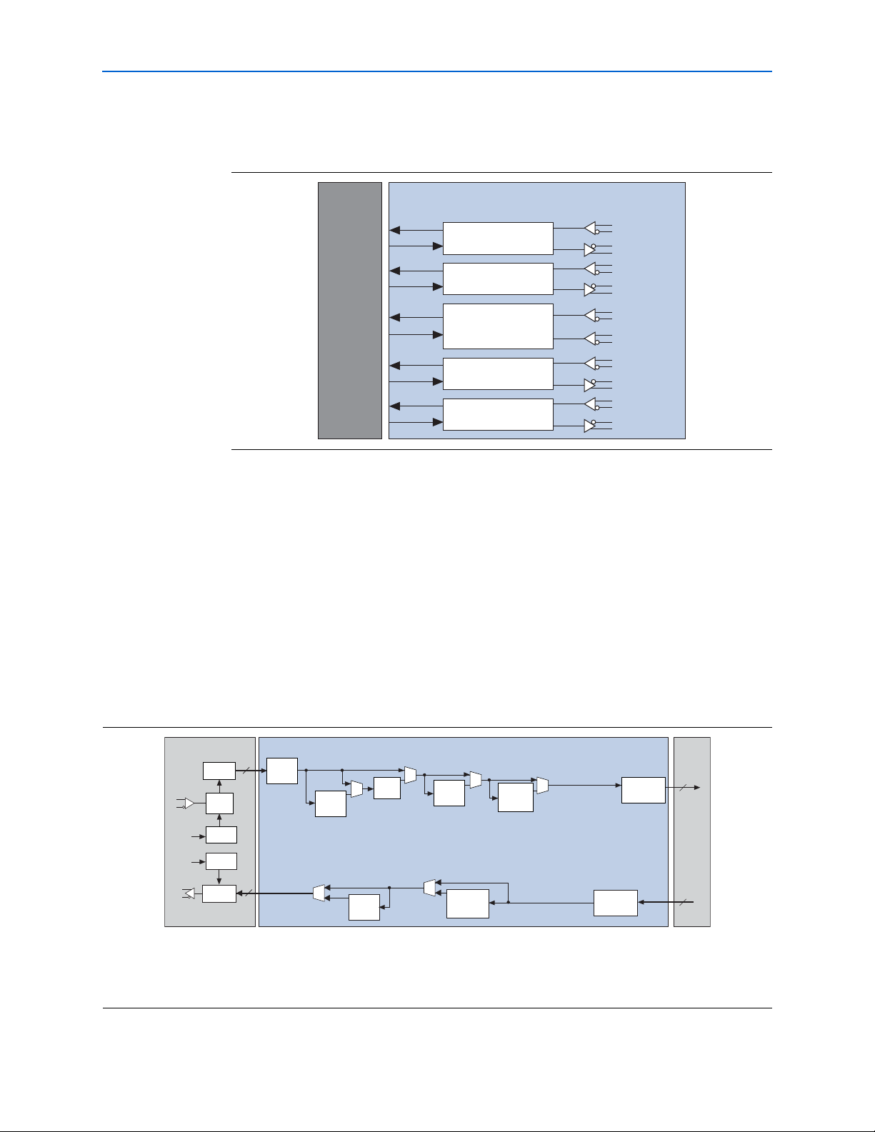
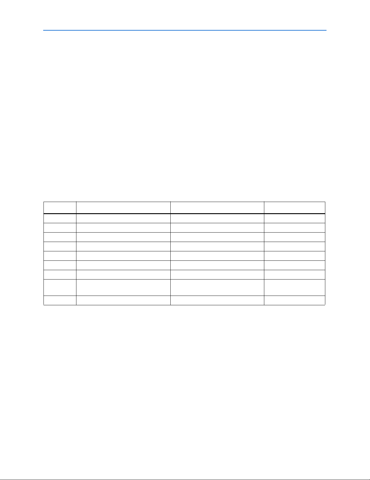
Channel 1
Channel 0
Channel 2
Supporting Blocks
(PLLs, State Machines,
Programming)
Channel 3
RX1
TX1
RX0
TX0
RX2
TX2
RX3
TX3
REFCLK_1
REFCLK_0
Transceiver Block
Arria GX
Logic Array
Transceivers
Figure 2–1 shows a high-level diagram of the transceiver block architecture divided
into four channels.
Figur e 2–1. Transceiver Block
Each transceiver block has:
■ Four transceiver channels with dedicated physical coding sublayer (PCS) and
physical media attachment (PMA) circuitry
■ One transmitter PLL that takes in a reference clock and generates high-speed serial
clock depending on the functional mode
■ Four receiver PLLs and clock recovery unit (CRU) to recover clock and data from
the received serial data stream
■ State machines and other logic to implement special features required to support
each protocol
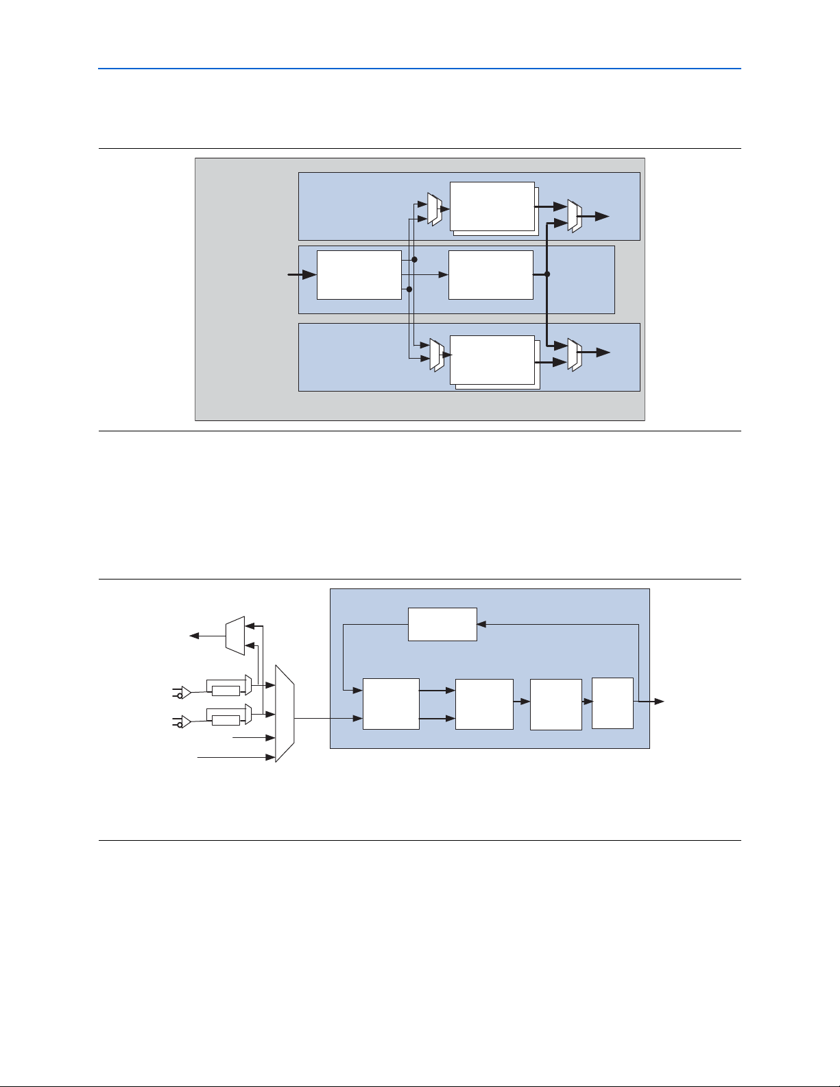
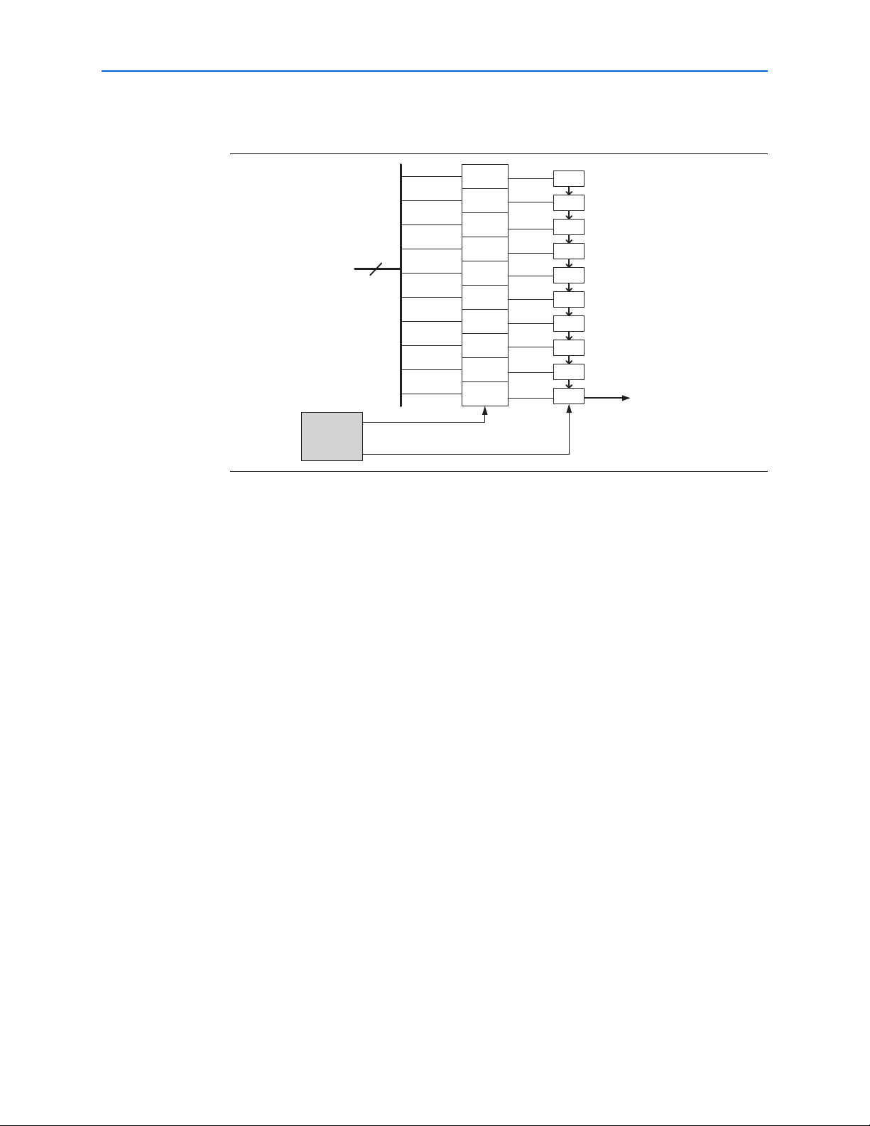
Figure 2–2 shows functional blocks that make up a transceiver channel.
Figur e 2–2. Arria GX Transceiver Channel Block Diagram
n
(1)
n
(1)
PCS Digital Section
Word
Aligner
XAUI
Lane
Deskew
8B/10B
Encoder
Rate
Matcher
8B/10B
Decoder
Byte
Serializer
Byte
Deserializer
Phase
Compensation
FIFO Buffer
Phase
Compensation
FIFO Buffer
FPGA Fabric
m
(2)
m
(2)
PMA Analog Section
Deserializer
Clock
Recovery
Unit
Receiver
Reference
Reference
Clock
Clock
PLL
Transmitter
PLL
Serializer
Notes to Figure 2–2:
(1) “n” represents the number of bits in each word that must be serialized by the transmitter portion of the PMA.
n = 8 or 10.
(2) “m” represents the number of bits in the word that passes between the FPGA logic and the PCS portion of the transceiver. m = 8, 10, 16, or 20.
Arria GX Device Handbook, Volume 1 © December 2009 Altera Corporation
Page 17

Chapter 2: Arria GX Architecture 2–3
Transceivers
Each transceiver channel is full-duplex and consists of a transmitter channel and a
receiver channel.
The transmitter channel contains the following sub-blocks:
■ Transmitter phase compensation first-in first-out (FIFO) buffer
■ Byte serializer (optional)
■ 8B/10B encoder (optional)
■ Serializer (parallel-to-serial converter)
■ Transmitter differential output buffer
The receiver channel contains the following:
■ Receiver differential input buffer
■ Receiver lock detector and run length checker
■ CRU
■ Deserializer
■ Pattern detector
Transmitter Path
■ Word aligner
■ Lane deskew
■ Rate matcher (optional)
■ 8B/10B decoder (optional)
■ Byte deserializer (optional)
■ Receiver phase compensation FIFO buffer
You can configure the transceiver channels to the desired functional modes using the
ALT2GXB MegaCore instance in the Quartus® II MegaWizard™ Plug-in Manager for
the Arria GX device family. Depending on the selected functional mode, the
Quartus II software automatically configures the transceiver channels to employ a
subset of the sub-blocks listed above.
This section describes the data path through the Arria GX transmitter. The sub-blocks
are described in order from the PLD-transmitter parallel interface to the serial
transmitter buffer.
Clock Multiplier Unit
Each transceiver block has a clock multiplier unit (CMU) that takes in a reference
clock and synthesizes two clocks: a high-speed serial clock to serialize the data and a
low-speed parallel clock to clock the transmitter digital logic (PCS).
The CMU is further divided into three sub-blocks:
■ One transmitter PLL
■ One central clock divider block
■ Four local clock divider blocks (one per channel)
© December 2009 Altera Corporation Arria GX Device Handbook, Volume 1
Page 18
2–4 Chapter 2: Arria GX Architecture
Transceivers
Figure 2–3 shows the block diagram of the clock multiplier unit.
Figur e 2–3. Clock Multiplier Unit
CMU Block
Reference Clock
from REFCLKs,
Global Clock (1),
Inter-Transceiver
The transmitter PLL multiplies the input reference clock to generate the high-speed
serial clock required to support the intended protocol. It implements a half-rate
voltage controlled oscillator (VCO) that generates a clock at half the frequency of the
serial data rate for which it is configured.
Figure 2–4 shows the block diagram of the transmitter PLL.
Figur e 2–4. Transmitter PLL
Lines
Transmitter Channels [3:2]
Transmitter
PLL
Transmitter Channels [1:0]
Local Clock
TX Clock
Divider Block
Gen Block
Central Clock
Divider
Block
Local Clock
TX Clock
Divider Block
Gen Block
Transmitter High-Speed Serial
and Low-Speed Parallel Clocks
Transmitter High-Speed Serial
and Low-Speed Parallel Clocks
Transmitt er PLL
(1)
To
Inter-Transcei ver Lines
Dedicated
REFCLK0
Dedicated
REFCLK1
Inter-Transceiver Lines[2:0]
Global Clock
(2)
/2
/2
INCLK
Phase
Frequency
Detector
/M
up
down
Charge
Pump + Loop
Filter
Voltage
Controlled
Oscillator
(1)
/L
Hi gh S peed
Serial Clock
Notes to Figure 2–4:
(1) You only need to select the protocol and the available i nput r efer ence clock frequency in the ALTGXB MegaWizard Plug-In Manager. Based on your
selections, the MegaWizard Plug-In Manager automatically selects the necessary /M and /L dividers (clock multiplication factors).
(2) The global clock line must be driven from an input pin only.
The reference clock input to the transmitter PLL can be derived from:
■ One of two available dedicated reference clock input pins (REFCLK0 or REFCLK1)
of the associated transceiver block
■ PLD global clock network (must be driven directly from an input clock pin and
cannot be driven by user logic or enhanced PLL)
Arria GX Device Handbook, Volume 1 © December 2009 Altera Corporation
Page 19
Chapter 2: Arria GX Architecture 2–5
Transceivers
■ Inter-transceiver block lines driven by reference clock input pins of other
transceiver blocks
1 Altera
REFCLK1) to provide reference clock for the transmitter PLL.
Table 2–2 lists the adjustable parameters in the transmitter PLL.
Tab le 2 –2. Transmit ter PLL Specifications
Input reference frequency range 50 MHz to 622.08 MHz
Data rate support 600 Mbps to 3.125 Gbps
Bandwidth Low, medium, or high
The transmitter PLL output feeds the central clock divider block and the local clock
divider blocks. These clock divider blocks divide the high-speed serial clock to
generate the low-speed parallel clock for the transceiver PCS logic and
PLD-transceiver interface clock.
Transmitter Phase Compensation FIFO Buffer
A transmitter phase compensation FIFO is located at each transmitter channel’s logic
array interface. It compensates for the phase difference between the transmitter PCS
clock and the local PLD clock. The transmitter phase compensation FIFO is used in all
supported functional modes. The transmitter phase compensation FIFO buffer is eight
words deep in PCI Express (PIPE) mode and four words deep in all other modes.
®
recommends using the dedicated reference clock input pins (REFCLK0 or
Parameter Specifications
f For more information about architecture and clocking, refer to the Arria GX Transceiver
Architecture chapter.
Byte Serializer
The byte serializer takes in two-byte wide data from the transmitter phase
compensation FIFO buffer and serializes it into a one-byte wide data at twice the
speed. The transmit data path after the byte serializer is 8 or 10 bits. This allows
clocking the PLD-transceiver interface at half the speed when compared with the
transmitter PCS logic. The byte serializer is bypassed in GIGE mode. After
serialization, the byte serializer transmits the least significant byte (LSByte) first and
the most significant byte (MSByte) last.
© December 2009 Altera Corporation Arria GX Device Handbook, Volume 1
Page 20
2–6 Chapter 2: Arria GX Architecture
xxxxxxxxxx xxxxxxxxxx
8'h01
{8'h00,8'h01}datain[15:0]
dataout[7:0]
8'h00 8'h03 8'h02
D1 D2 D3
D1
LSByte
D1
MSByte
D2
LSByte
D2
MSByte
{8'h02,8'h03} xxxx
Transceivers
Figure 2–5 shows byte serializer input and output. datain[15:0] is the input to the
byte serializer from the transmitter phase compensation FIFO; dataout[7:0] is the
output of the byte serializer.
Figur e 2–5. Byte Serializer Operation (Note 1)
Note to Figure 2–5:
(1) datain may be 16 or 20 bits. dataout may be 8 or 10 bits.
8B/10B Encoder
The 8B/10B encoder block is used in all supported functional modes. The 8B/10B
encoder block takes in 8-bit data from the byte serializer or the transmitter phase
compensation FIFO buffer. It generates a 10-bit code group with proper running
disparity from the 8-bit character and a 1-bit control identifier (tx_ctrlenable).
When tx_ctrlenable is low, the 8-bit character is encoded as data code group
(Dx.y). When tx_ctrlenable is high, the 8-bit character is encoded as a control
code group (Kx.y). The 10-bit code group is fed to the serializer. The 8B/10B encoder
conforms to the IEEE 802.3 1998 edition standard.
f For additional information regarding 8B/10B encoding rules, refer to the Specifications
and Additional Information chapter.
Figure 2–6 shows the 8B/10B conversion format.
Figur e 2–6. 8B/10B Encoder
76543210
HGFED CB A
8B-10B Conversion
jhgfiedcba
9 8 76543210
MSB
Ctrl
LSB
During reset (tx_digitalreset), the running disparity and data registers are
cleared and the 8B/10B encoder continously outputs a K28.5 pattern from the
RD-column. After out of reset, the 8B/10B encoder starts with a negative disparity
(RD-) and transmits three K28.5 code groups for synchronizing before it starts
encoding the input data or control character.
Arria GX Device Handbook, Volume 1 © December 2009 Altera Corporation
Page 21
Chapter 2: Arria GX Architecture 2–7
Transceivers
Transmit State Machine
The transmit state machine operates in either PCI Express (PIPE) mode, XAUI mode,
or GIGE mode, depending on the protocol used.
GIGE Mode
In GIGE mode, the transmit state machine converts all idle ordered sets (/K28.5/,
/Dx.y/) to either /I1/ or /I2/ ordered sets. The /I1/ set consists of a negative-ending
disparity /K28.5/ (denoted by /K28.5/-), followed by a neutral /D5.6/. The /I2/ set
consists of a positive-ending disparity /K28.5/ (denoted by /K28.5/+) and a
negative-ending disparity /D16.2/ (denoted by /D16.2/-). The transmit state
machines do not convert any of the ordered sets to match /C1/ or /C2/, which are
the configuration ordered sets. (/C1/ and /C2/ are defined by [/K28.5/, /D21.5/]
and [/K28.5/, /D2.2/], respectively). Both the /I1/ and /I2/ ordered sets guarantee a
negative-ending disparity after each ordered set.
XAUI Mode
The transmit state machine translates the XAUI XGMII code group to the XAUI PCS
code group. Table 2–3 lists the code conversion.
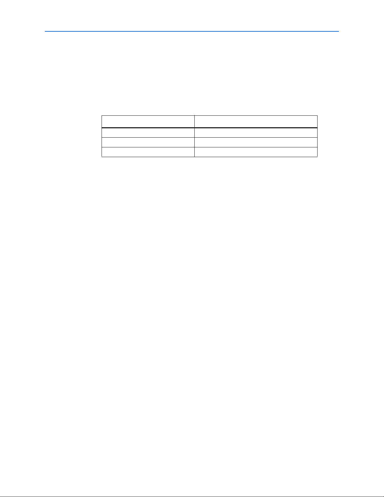
Tab le 2 –3. On-Chip Termination Support by I/O Banks
XGMII TXC XGMII TXD PCS Code-Group Description
0 00 through FF Dxx.y Normal data
1 07 K28.0 or K28.3 or K28.5 Idle in ||I||
1 07 K28.5 Idle in ||T||
1 9C K28.4 Sequence
1FB K27.7 Start
1FD K29.7 Terminate
1 FE K30.7 Error
1 Refer to IEEE 802.3 reserved code
groups
1 Other value K30.7 Invalid XGMII character
Refer to IEEE 802.3 reserved code
groups
Reserved code groups
The XAUI PCS idle code groups, /K28.0/ (/R/) and /K28.5/ (/K/), are automatically
randomized based on a PRBS7 pattern with an ×7 + ×6 + 1 polynomial. The /K28.3/
(/A/) code group is automatically generated between 16 and 31 idle code groups. The
idle randomization on the /A/, /K/, and /R/ code groups is automatically done by
the transmit state machine.
Serializer (Parallel-to-Serial Converter)
The serializer block clocks in 8- or 10-bit encoded data from the 8B/10B encoder using
the low-speed parallel clock and clocks out serial data using the high-speed serial
clock from the central or local clock divider blocks. The serializer feeds the data LSB to
MSB to the transmitter output buffer.
© December 2009 Altera Corporation Arria GX Device Handbook, Volume 1
Page 22
2–8 Chapter 2: Arria GX Architecture
D9
D8
D7
D6
D5
D4
D3
D2
D1
D0
10
D9
D8
D7
D6
D5
D4
D3
D2
D1
D0
To Transm it t e r
Output Buffer
CMU
Central/
Local Cloc k
Divider
Low-speed parall el cloc k
High-speed s eri al cloc k
From
8B/10B
Encoder
Transceivers
Figure 2–7 shows the serializer block diagram.
Figur e 2–7. Serializer
Transmitter Buffer
The Arria GX transceiver buffers support the 1.2- and 1.5-V PCML I/O standard at
rates up to 3.125 Gbps. The common mode voltage (VCM) of the output driver may be
set to 600 or 700 mV.
f For more information about the Arria GX transceiver buffers, refer to the Arria GX
Transceiver Architecture chapter.
The output buffer, as shown in Figure 2–8, is directly driven by the high-speed data
serializer and consists of a programmable output driver, a programmable
pre-emphasis circuit, and OCT circuitry.
Arria GX Device Handbook, Volume 1 © December 2009 Altera Corporation
Page 23
Chapter 2: Arria GX Architecture 2–9
Serializer
Programmable
Pre-Emphasis
Output Buffer
Output
Pins
Programmable
Output
Driver
Transceivers
Figur e 2–8. Output Buffer
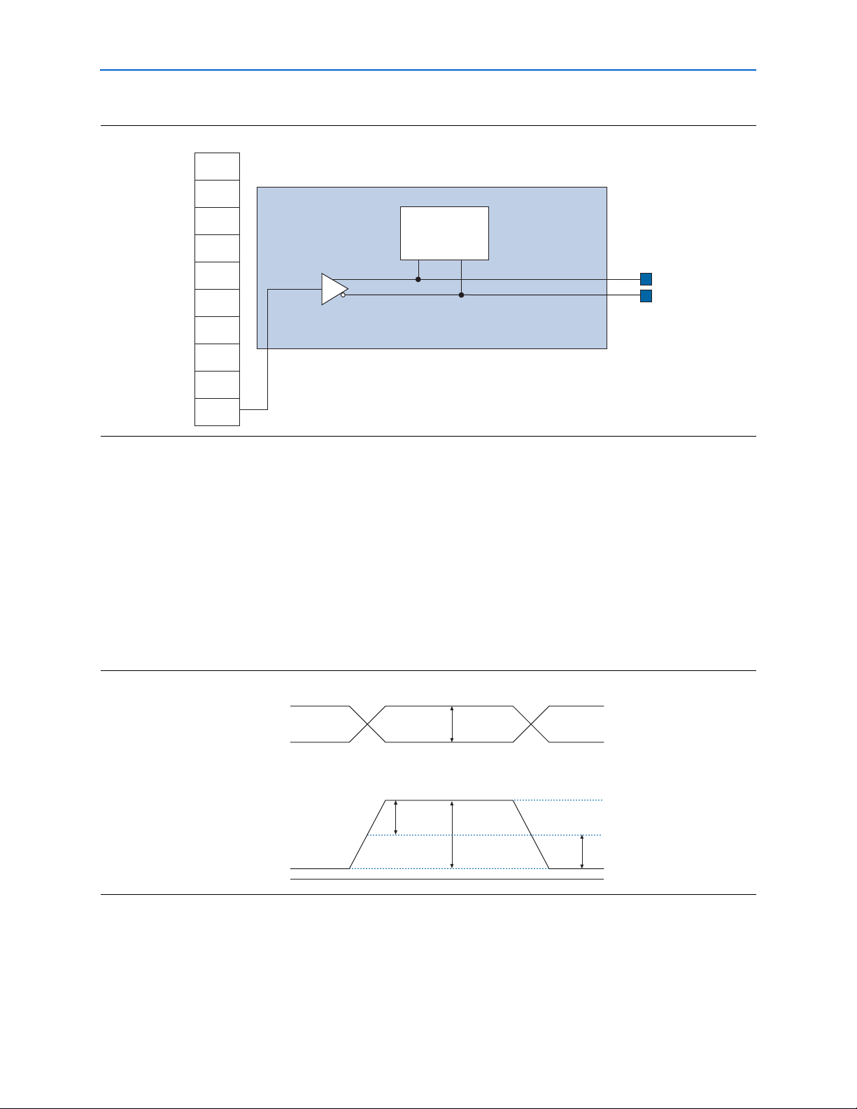
Figur e 2–9. Differential Signaling
V
OD
= V
high
Programmable Output Driver
The programmable output driver can be set to drive out differentially from 400 to
1200 mV. The differential output voltage (VOD) can be statically set by using the
ALTGXB megafunction.
You can configure the output driver with 100- OCT or external OCT.
Differential signaling conventions are shown in Figure 2–9. The differential amplitude
represents the value of the voltage between the true and complement signals.
Peak-to-peak differential voltage is defined as 2 (V
voltage swing. The common mode voltage is the average of V
Tr ue
Complement
(Differential)
−
V
low
Single-Ended Waveform
Differential Waveform
+V
OD
V
high
+V
OD
-
V
low
2 * V
OD
HIGH
– V
) = 2 single-ended
LOW
and V
HIGH
+400
0-V Differential
-V
OD
−400
LOW
.
© December 2009 Altera Corporation Arria GX Device Handbook, Volume 1
Page 24
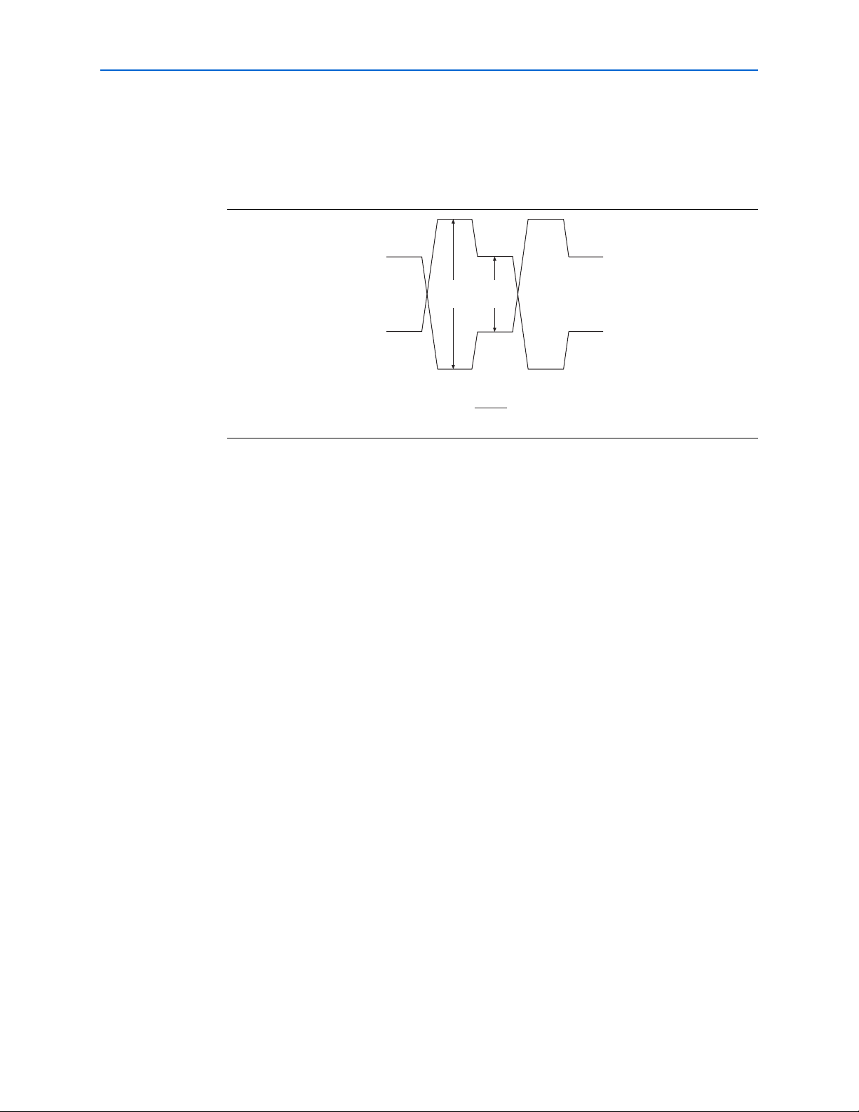
2–10 Chapter 2: Arria GX Architecture
V
MAX
V
MAX
V
MIN
V
MIN
Pre-Emphasis % = (
− 1) × 100
Transceivers
Programmable Pre-Emphasis
The programmable pre-emphasis module controls the output driver to boost high
frequency components and compensate for losses in the transmission medium, as
shown in Figure 2–10. Pre-emphasis is set statically using the ALTGXB megafunction.
Figur e 2–10. Pre-Emphasis Signaling
Receiver Path
Pre-emphasis percentage is defined as (V
MAX/VMIN
differential emphasized voltage (peak-to-peak) and V
– 1) × 100, where V
is the differential
MIN
MAX
is the
steady-state voltage (peak-to-peak).
PCI Express (PIPE) Receiver Detect
The Arria GX transmitter buffer has a built-in receiver detection circuit for use in PCI
Express (PIPE) mode. This circuit provides the ability to detect if there is a receiver
downstream by sending out a pulse on the channel and monitoring the reflection.
This mode requires a tri-stated transmitter buffer (in electrical idle mode).
PCI Express (PIPE) Electric Idles (or Individual Transmitter Tri-State)
The Arria GX transmitter buffer supports PCI Express (PIPE) electrical idles. This
feature is only active in PCI Express (PIPE) mode. The tx_forceelecidle port puts
the transmitter buffer in electrical idle mode. This port is available in all PCI Express
(PIPE) power-down modes and has specific usage in each mode.
This section describes the data path through the Arria GX receiver. The sub-blocks are
described in order from the receiver buffer to the PLD-receiver parallel interface.
Receiver Buffer
The Arria GX receiver input buffer supports the 1.2-V and 1.5-V PCML I/O standards
at rates up to 3.125 Gbps. The common mode voltage of the receiver input buffer is
programmable between 0.85 V and 1.2 V. You must select the 0.85 V common mode
voltage for AC- and DC-coupled PCML links and 1.2 V common mode voltage for
DC-coupled LVDS links.
Arria GX Device Handbook, Volume 1 © December 2009 Altera Corporation
Page 25
Chapter 2: Arria GX Architecture 2–11
Transceivers
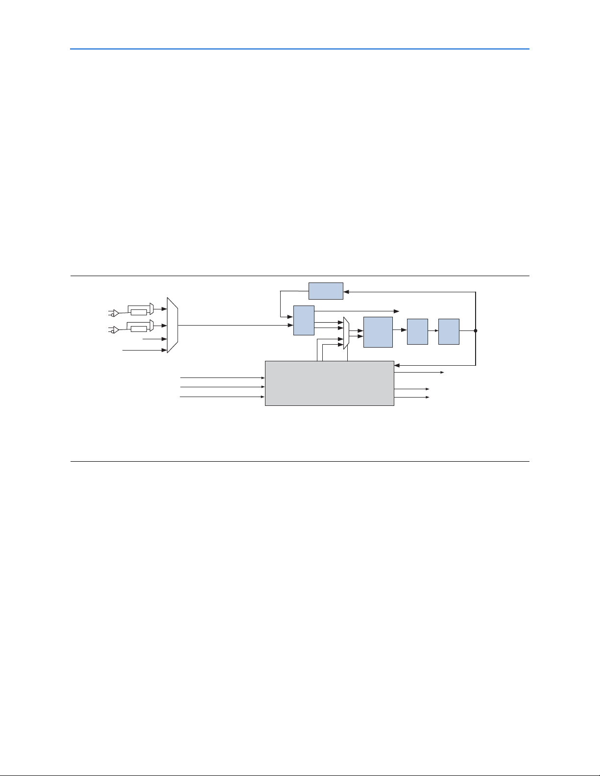
The receiver has 100- on-chip differential termination (RD OCT) for different
protocols, as shown in Figure 2–11. You can disable the receiver’s internal termination
if external terminations and biasing are provided. The receiver and transmitter
differential termination method can be set independently of each other.
Figur e 2–11. Receiver Input Buffer
100-Ω
Termination
Input
Pins
Programmable
Equalizer
Differential
Input
Buffer
If a design uses external termination, the receiver must be externally terminated and
biased to 0.85 V or 1.2 V. Figure 2–12 shows an example of an external termination and
biasing circuit.
Figur e 2–12. External Termination and Biasi ng Circuit
Receiver External Termination
and Biasing
50-W
Termination
Resistance
R1/R2 = 1K
V
´ {R2/(R1 + R 2)} = 0.85/1.2 V
DD
Receiver External Termination
Transmission
Line
Programmable Equalizer
The Arria GX receivers provide a programmable receiver equalization feature to
compensate for the effects of channel attenuation for high-speed signaling. PCB traces
carrying these high-speed signals have low-pass filter characteristics. Impedance
mismatch boundaries can also cause signal degradation. Equalization in the receiver
diminishes the lossy attenuation effects of the PCB at high frequencies.
V
DD
C1
and Biasing
R1
R2
Arria GX Device
Receiver
RXIP
RXIN
© December 2009 Altera Corporation Arria GX Device Handbook, Volume 1
Page 26
2–12 Chapter 2: Arria GX Architecture
PFD
CP+LF
up
dn
VCO
/M
Clock Recovery Unit (CRU) Control
High-speed serial recovered clk
Low-speed parallel recovered clk
dn
up
/L
rx_pll_lock ed
rx_freqlocked
Dedicated
REFCLK0
/2
Dedicated
REFCLK1
/2
Inter-Transceiver Lines
[2:0]
Global Clock
(2)
rx_locktorefclk
rx_locktodata
rx_datain
rx_cruclk
Transceivers
The receiver equalization circuit is comprised of a programmable amplifier. Each
stage is a peaking equalizer with a different center frequency and programmable gain.
This allows varying amounts of gain to be applied, depending on the overall
frequency response of the channel loss. Channel loss is defined as the summation of
all losses through the PCB traces, vias, connectors, and cables present in the physical
link. The Quartus II software allows five equalization settings for Arria GX devices.
Receiver PLL and Clock Recovery Unit (CRU)
Each transceiver block has four receiver PLLs and CRU units, each of which is
dedicated to a receiver channel. The receiver PLL is fed by an input reference clock.
The receiver PLL, in conjunction with the CRU, generates two clocks: a high-speed
serial recovered clock that clocks the deserializer and a low-speed parallel recovered
clock that clocks the receiver's digital logic.
Figure 2–13 shows a block diagram of the receiver PLL and CRU circuits.
Figur e 2–13. Receiver PLL and Clock Recovery Unit
Notes to Figure 2–13:
(1) You only need to select the protocol and the available i nput r efer ence clock frequency in the ALTGXB MegaWizard Plug-In Manager. Based on your
selections, the ALTGXB MegaWizard Plug-In Manager automatically selects the necessary /M and /L dividers.
(2) The global clock line must be driven from an input pin only.
The reference clock input to the receiver PLL can be derived from:
■ One of the two available dedicated reference clock input pins (REFCLK0 or
REFCLK1) of the associated transceiver block
■ PLD global clock network (must be driven directly from an input clock pin and
cannot be driven by user logic or enhanced PLL)
■ Inter-transceiver block lines driven by reference clock input pins of other
transceiver blocks
All the parameters listed are programmable in the Quartus II software. The receiver
PLL has the following features:
■ Operates from 600 Mbps to 3.125 Gbps.
■ Uses a reference clock between 50 MHz and 622.08 MHz.
■ Programmable bandwidth settings: low, medium, and high.
■ Programmable rx_locktorefclk (forces the receiver PLL to lock to reference
clock) and rx_locktodata (forces the receiver PLL to lock to data).
Arria GX Device Handbook, Volume 1 © December 2009 Altera Corporation
Page 27
Chapter 2: Arria GX Architecture 2–13
Transceivers
■ The voltage-controlled oscillator (V
■ Programmable frequency multiplication W of 1, 4, 5, 8, 10, 16, 20, and 25. Not all
) operates at half rate.
CO
settings are supported for any particular frequency.
■ Two lock indication signals are provided. They are found in PFD mode
(lock-to-reference clock), and PD (lock-to-data).
The CRU controls whether the receiver PLL locks to the input reference clock
(lock-to-reference mode) or the incoming serial data (lock-to data mode). You can set
the CRU to switch between lock-to-data and lock-to-reference modes automatically or
manually. In automatic lock mode, the phase detector and dedicated parts per million
(PPM) detector within each receiver channel control the switch between lock-to-data
and lock-to-reference modes based on some pre-set conditions. In manual lock mode,
you can control the switch manually using the rx_locktorefclk and
rx_locktodata signals.
f For more information, refer to the “Clock Recovery Unit” section in the Arria GX
Transceiver Protocol Support and Additional Features chapter.
Table 2–4 lists the behavior of the CRU block with respect to the rx_locktorefclk
and rx_locktodata signals.
Tab le 2 –4. CRU Manual Lock Signals
rx_locktorefclk rx_locktodata CRU Mode
1 0 Lock-to-reference clock
x 1 Lock-to-data
0 0 Automatic
If the rx_locktorefclk and rx_locktodata ports are not used, the default
setting is automatic lock mode.
Deserializer
The deserializer block clocks in serial input data from the receiver buffer using the
high-speed serial recovered clock and deserializes into 8- or 10-bit parallel data using
the low-speed parallel recovered clock. The serial data is assumed to be received with
LSB first, followed by MSB. It feeds the deserialized 8- or 10-bit data to the word
aligner, as shown in Figure 2–14.
© December 2009 Altera Corporation Arria GX Device Handbook, Volume 1
Page 28
2–14 Chapter 2: Arria GX Architecture
D9
D8
D7
D6
D5
D4
D3
D2
D1
D0
D9
D8
D7
D6
D5
D4
D3
D2
D1
D0
To Word
Aligner
Clock
Recovery
Unit
Low -speed parallel recover ed clock
High-speed serial recovered clock
Received D ata
10
Transceivers
Figur e 2–14. Deserializer (Note 1)
Note to Figure 2–14:
(1) This is a 10-bit deserializer. The deserializer can also convert 8 bits of data.
Word Aligner
The deserializer block creates 8- or 10-bit parallel data. The deserializer ignores
protocol symbol boundaries when converting this data. Therefore, the boundaries of
the transferred words are arbitrary. The word aligner aligns the incoming data based
on specific byte or word boundaries. The word alignment module is clocked by the
local receiver recovered clock during normal operation. All the data and programmed
patterns are defined as “big-endian” (most significant word followed by least
significant word). Most-significant-bit-first protocols should reverse the bit order of
word align patterns programmed.
This module detects word boundaries for 8B/10B-based protocols. This module is
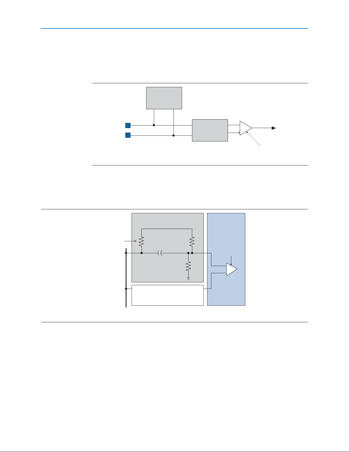
also used to align to specific programmable patterns in PRBS7/23 test mode.
Pattern Detection
The programmable pattern detection logic can be programmed to align word
boundaries using a single 7- or 10-bit pattern. The pattern detector can either do an
exact match, or match the exact pattern and the complement of a given pattern. Once
the programmed pattern is found, the data stream is aligned to have the pattern on
the LSB portion of the data output bus.
XAUI, GIGE, PCI Express (PIPE), and Serial RapidIO standards have embedded state
machines for symbol boundary synchronization. These standards use K28.5 as their
10-bit programmed comma pattern. Each of these standards uses different algorithms
before signaling symbol boundary acquisition to the FPGA.
Pattern detection logic searches from the LSB to the MSB. If multiple patterns are
found within the search window, the pattern in the lower portion of the data stream
(corresponding to the pattern received earlier) is aligned and the rest of the matching
patterns are ignored.
Arria GX Device Handbook, Volume 1 © December 2009 Altera Corporation
Page 29
Chapter 2: Arria GX Architecture 2–15
Transceivers
Once a pattern is detected and the data bus is aligned, the word boundary is locked.
The two detection status signals (rx_syncstatus and rx_patterndetect)
indicate that an alignment is complete.
Figure 2–15 is a block diagram of the word aligner.
Figur e 2–15. Word Aligner
datain dataout
bitslip
enapatternalign
clock
Word
Aligner
syncstatus
patterndetect
Control and Status Signals
The rx_enapatternalign signal is the FPGA control signal that enables word
alignment in non-automatic modes. The rx_enapatternalign signal is not used in
automatic modes (PCI Express [PIPE], XAUI, GIGE, and Serial RapidIO).
In manual alignment mode, after the rx_enapatternalign signal is activated, the
rx_syncstatus signal goes high for one parallel clock cycle to indicate that the
alignment pattern has been detected and the word boundary has been locked. If
rx_enapatternalign is deactivated, the rx_syncstatus signal acts as a
re-synchronization signal to signify that the alignment pattern has been detected but
not locked on a different word boundary.
When using the synchronization state machine, the rx_syncstatus signal indicates
the link status. If the rx_syncstatus signal is high, link synchronization is
achieved. If the rx_syncstatus signal is low, link synchronization has not yet been
achieved, or there were enough code group errors to lose synchronization.
f For more information about manual alignment modes, refer to the Arria GX Device
Handbook.
The rx_patterndetect signal pulses high during a new alignment and whenever
the alignment pattern occurs on the current word boundary.
Programmable Run Length Violation
The word aligner supports a programmable run length violation counter. Whenever
the number of the continuous ‘0’ (or ‘1’) exceeds a user programmable value, the
rx_rlv signal goes high for a minimum pulse width of two recovered clock cycles.
The maximum run values supported are 128 UI for 8-bit serialization or 160 UI for
10-bit serialization.
Running Disparity Check
The running disparity error rx_disperr and running disparity value
rx_runningdisp are sent along with aligned data from the 8B/10B decoder to the
FPGA. You can ignore or act on the reported running disparity value and running
disparity error signals.
© December 2009 Altera Corporation Arria GX Device Handbook, Volume 1
Page 30

2–16 Chapter 2: Arria GX Architecture
Transceivers
Bit-Slip Mode
The word aligner can operate in either pattern detection mode or in bit-slip mode.
The bit-slip mode provides the option to manually shift the word boundary through
the FPGA. This feature is useful for:
■ Longer synchronization patterns than the pattern detector can accommodate
■ Scrambled data stream
■ Input stream consisting of over-sampled data
The word aligner outputs a word boundary as it is received from the analog receiver
after reset. You can examine the word and search its boundary in the FPGA. To do so,
assert the rx_bitslip signal. The rx_bitslip signal should be toggled and held
constant for at least two FPGA clock cycles.
For every rising edge of the rx_bitslip signal, the current word boundary is
slipped by one bit. Every time a bit is slipped, the bit received earliest is lost. If bit
slipping shifts a complete round of bus width, the word boundary is back to the
original boundary.
The rx_syncstatus signal is not available in bit-slipping mode.
Channel Aligner
The channel aligner is available only in XAUI mode and aligns the signals of all four
channels within a transceiver. The channel aligner follows the IEEE 802.3ae, clause 48
specification for channel bonding.
The channel aligner is a 16-word FIFO buffer with a state machine controlling the
channel bonding process. The state machine looks for an /A/ (/K28.3/) in each
channel and aligns all the /A/ code groups in the transceiver. When four columns of
/A/ (denoted by //A//) are detected, the rx_channelaligned signal goes high,
signifying that all the channels in the transceiver have been aligned. The reception of
four consecutive misaligned /A/ code groups restarts the channel alignment
sequence and sends the rx_channelaligned signal low.
Arria GX Device Handbook, Volume 1 © December 2009 Altera Corporation
Page 31

Chapter 2: Arria GX Architecture 2–17
KRKKKRRRKKRA
Lane 3
KRKKKRRRKKRA
Lane 2
KRKKKRRRKKRA
Lane 1
KRKKKRRRKKRA
Lane 0
KRKKKRRRKKRA
Lane 3
KRKKKRRRKKRA
Lane 2
KRKKKRRRKKRA
Lane 1
KRKKKRRRKKRA
Lane 0
Before
After
Transceivers
Figure 2–16 shows misaligned channels before the channel aligner and the aligned
channels after the channel aligner.
Figur e 2–16. Before and After the Channel Aligner
Rate Matcher
In asynchronous systems, the upstream transmitter and local receiver can be clocked
with independent reference clock sources. Frequency differences in the order of a few
hundred PPM can potentially corrupt the data at the receiver.
The rate matcher compensates for small clock frequency differences between the
upstream transmitter and the local receiver clocks by inserting or removing skip
characters from the inter packet gap (IPG) or idle streams. It inserts a skip character if
the local receiver is running a faster clock than the upstream transmitter. It deletes a
skip character if the local receiver is running a slower clock than the upstream
transmitter. The Quartus II software automatically configures the appropriate skip
character as specified in the IEEE 802.3 for GIGE mode and PCI-Express Base
Specification for PCI Express (PIPE) mode. The rate matcher is bypassed in Serial
RapidIO and must be implemented in the PLD logic array or external circuits
depending on your system design.
Table 2–5 lists the maximum frequency difference that the rate matcher can tolerate in
XAUI, PCI Express (PIPE), GIGE, and Basic functional modes.
Tab le 2 –5. Rate Matcher PPM Tolerance
Function Mode PPM
XAUI ± 100
PCI Express (PIPE) ± 300
GIGE ± 100
Basi c ± 300
© December 2009 Altera Corporation Arria GX Device Handbook, Volume 1
Page 32

2–18 Chapter 2: Arria GX Architecture
Transceivers
XAUI Mode
In XAUI mode, the rate matcher adheres to clause 48 of the IEEE 802.3ae specification
for clock rate compensation. The rate matcher performs clock compensation on
columns of /R/ (/K28.0/), denoted by //R//. An //R// is added or deleted
automatically based on the number of words in the FIFO buffer.
PCI Express (PIPE) Mode Rate Matcher
In PCI Express (PIPE) mode, the rate matcher can compensate up to ± 300 PPM
(600 PPM total) frequency difference between the upstream transmitter and the
receiver. The rate matcher logic looks for skip ordered sets (SOS), which contains a
/K28.5/ comma followed by three /K28.0/ skip characters. The rate matcher logic
deletes or inserts /K28.0/ skip characters as necessary from/to the rate matcher FIFO.
The rate matcher in PCI Express (PIPE) mode has a FIFO buffer overflow and
underflow protection. In the event of a FIFO buffer overflow, the rate matcher deletes
any data after detecting the overflow condition to prevent FIFO pointer corruption
until the rate matcher is not full. In an underflow condition, the rate matcher inserts
9'h1FE (/K30.7/) until the FIFO buffer is not empty. These measures ensure that the
FIFO buffer can gracefully exit the overflow and underflow condition without
requiring a FIFO reset. The rate matcher FIFO overflow and underflow condition is
indicated on the pipestatus port.
You can bypass the rate matcher in PCI Express (PIPE) mode if you have a
synchronous system where the upstream transmitter and local receiver derive their
reference clocks from the same source.
GIGE Mode Rate Matcher
In GIGE mode, the rate matcher can compensate up to ± 100 PPM (200 PPM total)
frequency difference between the upstream transmitter and the receiver. The rate
matcher logic inserts or deletes /I2/ idle ordered sets to/from the rate matcher FIFO
during the inter-frame or inter-packet gap (IFG or IPG). /I2/ is selected as the rate
matching ordered set because it maintains the running disparity, unlike /I1/ that
alters the running disparity. Because the /I2/ ordered-set contains two 10-bit code
groups (/K28.5/, /D16.2/), 20 bits are inserted or deleted at a time for rate matching.
1 The rate matcher logic has the capability to insert or delete /C1/ or /C2/
configuration ordered sets when ‘GIGE Enhanced’ mode is chosen as the sub-protocol
in the MegaWizard Plug-In Manager.
If the frequency PPM difference between the upstream transmitter and the local
receiver is high, or if the packet size is too large, the rate matcher FIFO buffer can face
an overflow or underflow situation.
Basic Mode
In basic mode, you can program the skip and control pattern for rate matching. There
is no restriction on the deletion of a skip character in a cluster. The rate matcher
deletes the skip characters as long as they are available. For insertion, the rate matcher
inserts skip characters such that the number of skip characters at the output of rate
matcher does not exceed five.
Arria GX Device Handbook, Volume 1 © December 2009 Altera Corporation
Page 33

Chapter 2: Arria GX Architecture 2–19
Transceivers
8B/10B Decoder
The 8B/10B decoder is used in all supported functional modes. The 8B/10B decoder
takes in 10-bit data from the rate matcher and decodes it into 8-bit data + 1-bit control
identifier, thereby restoring the original transmitted data at the receiver. The 8B/10B
decoder indicates whether the received 10-bit character is a data or control code
through the rx_ctrldetect port. If the received 10-bit code group is a control
character (Kx.y), the rx_ctrldetect signal is driven high and if it is a data
character (Dx.y), the rx_ctrldetect signal is driven low.
Figure 2–17 shows a 10-bit code group decoded to an 8-bit data and a 1-bit control
indicator.
Figur e 2–17. 10-Bit to 8-Bit Conversion
jhgfiedcb a
9876543210
MSB Received Last
ctrl
8B/10B Conversion
76543210
HGFED CB A
LSB Received First
Parallel Data
If the received 10-bit code is not a part of valid Dx.y or Kx.y code groups, the 8B/10B
decoder block asserts an error flag on the rx_errdetect port. If the received 10-bit
code is detected with incorrect running disparity, the 8B/10B decoder block asserts an
error flag on the rx_disperr and rx_errdetect ports. The error flag signals
(rx_errdetect and rx_disperr) have the same data path delay from the 8B/10B
decoder to the PLD-transceiver interface as the bad code group.
Receiver State Machine
The receiver state machine operates in Basic, GIGE, PCI Express (PIPE), and XAUI
modes. In GIGE mode, the receiver state machine replaces invalid code groups with
K30.7. In XAUI mode, the receiver state machine translates the XAUI PCS code group
to the XAUI XGMII code group.
© December 2009 Altera Corporation Arria GX Device Handbook, Volume 1
Page 34

2–20 Chapter 2: Arria GX Architecture
Transceivers
Byte Deserializer
Byte deserializer takes in one-byte wide data from the 8B/10B decoder and
deserializes it into a two-byte wide data at half the speed. This allows clocking the
PLD-receiver interface at half the speed as compared to the receiver PCS logic. The
byte deserializer is bypassed in GIGE mode.
The byte ordering at the receiver output might be different than what was
transmitted. This is a non-deterministic swap, because it depends on PLL lock times
and link delay. If required, you must implement byte ordering logic in the PLD to
correct this situation.
f For more information about byte serializer, refer to the Arria GX Transceiver
Architecture chapter.
Receiver Phase Compensation FIFO Buffer
A receiver phase compensation FIFO buffer is located at each receiver channel’s logic
array interface. It compensates for the phase difference between the receiver PCS
clock and the local PLD receiver clock. The receiver phase compensation FIFO is used
in all supported functional modes. The receiver phase compensation FIFO buffer is
eight words deep in PCI Express (PIPE) mode and four words deep in all other
modes.
f For more information about architecture and clocking, refer to the Arria GX Transceiver
Architecture chapter.
Loopback Modes
Arria GX transceivers support the following loopback configurations for diagnostic
purposes:
■ Serial loopback
■ Reverse serial loopback
■ Reverse serial loopback (pre-CDR)
■ PCI Express (PIPE) reverse parallel loopback (available only in [PIPE] mode)
Serial Loopback
Figure 2–18 shows the transceiver data path in serial loopback.
Figur e 2–18. Transceiver Data Path in Serial Loopback
PLD
Logic
Array
RX Phase
Compen-
sation
FIFO
TX Phase
Compen-
sation
FIFO
Serializer
Byte
De-
Byte
Serializer
8B/10B
Decoder
8B/10B
Encoder
Transmitter PCS Transmitter PMA
Serializer
Serial Loopback
Rate
Match
FIFO
Receiver PCS
Word
Aligner
Receiver PMA
De-
Serializer
Clock
Recovery
Unit
Arria GX Device Handbook, Volume 1 © December 2009 Altera Corporation
Page 35

Chapter 2: Arria GX Architecture 2–21
Transceivers
In GIGE and Serial RapidIO modes, you can dynamically put each transceiver
channel individually in serial loopback by controlling the rx_seriallpbken port. A
high on the rx_seriallpbken port puts the transceiver into serial loopback and a
low takes the transceiver out of serial loopback.
As seen in Figure 2–18, the serial data output from the transmitter serializer is looped
back to the receiver CRU in serial loopback. The transmitter data path from the PLD
interface to the serializer in serial loopback is the same as in non-loopback mode. The
receiver data path from the clock recovery unit to the PLD interface in serial loopback
is the same as in non-loopback mode. Because the entire transceiver data path is
available in serial loopback, this option is often used to diagnose the data path as a
probable cause of link errors.
1 When serial loopback is enabled, the transmitter output buffer is still active and
drives the serial data out on the tx_dataout port.
Reverse Serial Loopback
Reverse serial loopback mode uses the analog portion of the transceiver. An external
source (pattern generator or transceiver) generates the source data. The high-speed
serial source data arrives at the high-speed differential receiver input buffer, passes
through the CRU unit and the retimed serial data is looped back, and is transmitted
though the high-speed differential transmitter output buffer.
Figure 2–19 shows the data path in reverse serial loopback mode.
Figur e 2–19. Arria GX Block in Reverse Serial Loopback Mode
Transmitter Digital Logic
FPGA
Logic
Array
Receiver Digital Logic
BIST
Incremental
Generator
TX Phase
Compensation
BIST
Incremental
Verify
RX Phase
Compen-
sation
FIFO
FIFO
Byte
Serializer
20
Byte
De-
serializer
8B/10B
Encoder
8B/10B
Decoder
PRBS
Generator
BIST
Rate
Match
FIFO
Deskew
FIFO
BIST
PRBS
Verify
Word
Aligner
Analog Receiver and
Transmitter Logic
Serializer
Reverse
Serial
Loopback
De-
serializer
Clock
Recovery
Unit
© December 2009 Altera Corporation Arria GX Device Handbook, Volume 1
Page 36

2–22 Chapter 2: Arria GX Architecture
TX Phase
Compe -
nsation
FIFO
Byte
Ser ializer
8B/10B
Encoder
RX Phase
Compe -
nsation
FIFO
Word
Aligner
Transmitter PCS Transmitter PMA
Receiver PCS
Receiver PMA
PIPE Reverse
Parallel Loopback
PIPE
Interface
Byte
De-
Serializer
8B/10B
Decoder
Rate
Match
FIFO
Serializer
Clock
Recovery
Unit
De-
Serializer
Transceivers
Reverse Serial Pre-CDR Loopback
Reverse serial pre-CDR loopback mode uses the analog portion of the transceiver. An
external source (pattern generator or transceiver) generates the source data. The
high-speed serial source data arrives at the high-speed differential receiver input
buffer, loops back before the CRU unit, and is transmitted though the high-speed
differential transmitter output buffer. It is for test or verification use only to verify the
signal being received after the gain and equalization improvements of the input
buffer. The signal at the output is not exactly what is received because the signal goes
through the output buffer and the VOD is changed to the VOD setting level.
Pre-emphasis settings have no effect.
Figure 2–20 shows the Arria GX block in reverse serial pre-CDR loopback mode.
Figur e 2–20. Arria GX Block in Reverse Serial Pre-CDR Loopback Mode
Transmitter Digital Logic
BIST
Incremental
Generator
FPGA
Logic
Array
TX Phase
Compensation
BIST
Incremental
Verify
RX Phase
Compen-
sation
FIFO
FIFO
Byte
Serializer
20
Byte
De-
serializer
8B/10B
Encoder
8B/10B
Decoder
Receiver Digital Logic
PCI Express (PIPE) Reverse Parallel Loopback
Figure 2–21 shows the data path for PCI Express (PIPE) reverse parallel loopback. The
reverse parallel loopback configuration is compliant with the PCI Express (PIPE)
specification and is available only on PCI Express (PIPE) mode.
Figur e 2–21. PCI Express (PIPE) Reverse Parallel Loopback
BIST
PRBS
Generator
Rate
Match
FIFO
Deskew
FIFO
BIST
PRBS
Verify
Word
Aligner
Analog Receiver and
Transmitter Logic
Serializer
Reverse
Serial
Pre-CDR
Loopback
De-
serializer
Clock
Recovery
Unit
Arria GX Device Handbook, Volume 1 © December 2009 Altera Corporation
Page 37

Chapter 2: Arria GX Architecture 2–23
Transceivers
You can dynamically put the PCI Express (PIPE) mode transceiver in reverse parallel
loopback by controlling the tx_detectrxloopback port instantiated in the
MegaWizard Plug-In Manager. A high on the tx_detectrxloopback port in P0
power state puts the transceiver in reverse parallel loopback. A high on the
tx_detectrxloopback port in any other power state does not put the transceiver
in reverse parallel loopback.
As seen in Figure 2–21, the serial data received on the rx_datain port in reverse
parallel loopback goes through the CRU, deserializer, word aligner, and the rate
matcher blocks. The parallel data at the output of the receiver rate matcher block is
looped back to the input of the transmitter serializer block. The serializer converts the
parallel data to serial data and feeds it to the transmitter output buffer that drives the
data out on the tx_dataout port. The data at the output of the rate matcher also
goes through the 8B/10B decoder, byte deserializer, and receiver phase compensation
FIFO before being fed to the PLD on the rx_dataout port.
Reset and Powerdown
Arria GX transceivers offer a power saving advantage with their ability to shut off
functions that are not needed.
The following three reset signals are available per transceiver channel and can be used
to individually reset the digital and analog portions within each channel:
■ tx_digitalreset
■ rx_analogreset
■ rx_digitalreset
The following two powerdown signals are available per transceiver block and can be
used to shut down an entire transceiver block that is not being used:
■ gxb_powerdown
■ gxb_enable
© December 2009 Altera Corporation Arria GX Device Handbook, Volume 1
Page 38

2–24 Chapter 2: Arria GX Architecture
Transceivers
Table 2–6 lists the reset signals available in Arria GX devices and the transceiver
circuitry affected by each signal.
Tab le 2 –6. Reset Signal Map to Arria GX Blocks
Reset Signal
Transmitter Phase Compensation FIFO Module/ Byte Serializer
Transmitter 8B/10B Encoder
Transmitter Serializer
Transmitter Analog Circuits
Transmitter PLL
Transmitter XAUI State Machine
BIST Generat ors
Receiver Deserializer
Receiver Word Aligner
Receiver Deskew FIFO Module
Receiver Rate Matcher
Receiver 8B/10B Decoder
Receiver Phase Comp FIFO Module/ Byte Deserializer
Receiver PLL / CRU
Receiver XAUI State Machin e
BIST Verifiers
rx_digital reset ————————v — vvv— vv—
rx_analogr eset ———————v —————v ——v
tx_digital reset vv———vv——————————
gxb_powerd own vvvvvvvvv— vvvvvvv
gxb_enable vvvvvvvvv— vvvvvvv
Calibration Block
Arria GX devices use the calibration block to calibrate OCT for the PLLs, and their
associated output buffers, and the terminating resistors on the transceivers. The
calibration block counters the effects of process, voltage, and temperature (PVT). The
calibration block references a derived voltage across an external reference resistor to
calibrate the OCT resistors on Arria GX devices. You can power down the calibration
block. However, powering down the calibration block during operations can yield
transmit and receive data errors.
Transceiver Clocking
This section describes the clock distribution in an Arria GX transceiver channel and
the PLD clock resource utilization by the transceiver blocks.
Transceiver Channel Clock Distribution
Each transceiver block has one transmitter PLL and four receiver PLLs.
Receiver Analog Circuits
Arria GX Device Handbook, Volume 1 © December 2009 Altera Corporation
Page 39

Chapter 2: Arria GX Architecture 2–25
Transceiver Block 2
Transceiver Block 1
/2
/2
Global C lock
(1)
Transmitter
PLL
Transceiver Block 0
Four
Receiver
PLLs
Global Clock
(1)
Inter-Transceiver Lines [2:0]
Dedicated
REFCLK1
Dedicated
REFCLK0
Inter-Transceiver Lines [0]
Inter-Transceiver Lines [1]
Inter-Transceiver Lines [2]
Transceivers
The transmitter PLL multiplies the input reference clock to generate a high-speed
serial clock at a frequency that is half the data rate of the configured functional mode.
This high-speed serial clock (or its divide-by-two version if the functional mode uses
byte serializer) is fed to the CMU clock divider block. Depending on the configured
functional mode, the CMU clock divider block divides the high-speed serial clock to
generate the low-speed parallel clock that clocks the transceiver PCS logic in the
associated channel. The low-speed parallel clock is also forwarded to the PLD logic
array on the tx_clkout or coreclkout ports.
The receiver PLL in each channel is also fed by an input reference clock. The receiver
PLL along with the clock recovery unit generates a high-speed serial recovered clock
and a low-speed parallel recovered clock. The low-speed parallel recovered clock
feeds the receiver PCS logic until the rate matcher. The CMU low-speed parallel clock
clocks the rest of the logic from the rate matcher until the receiver phase
compensation FIFO. In modes that do not use a rate matcher, the receiver PCS logic is
clocked by the recovered clock until the receiver phase compensation FIFO.
The input reference clock to the transmitter and receiver PLLs can be derived from:
■ One of two available dedicated reference clock input pins (REFCLK0 or REFCLK1)
of the associated transceiver block
■ PLD clock network (must be driven directly from an input clock pin and cannot be
driven by user logic or enhanced PLL)
■ Inter-transceiver block lines driven by reference clock input pins of other
transceiver blocks
Figure 2–22 shows the input reference clock sources for the transmitter and receiver
PLL.
Figur e 2–22. Input Reference Clock Sources
© December 2009 Altera Corporation Arria GX Device Handbook, Volume 1
Page 40

2–26 Chapter 2: Arria GX Architecture
Transceivers
f For more information about transceiver clocking in all supported functional modes,
refer to the Arria GX Transceiver Architecture chapter.
PLD Clock Utilization by Transceiver Blocks
Arria GX devices have up to 16 global clock (GCLK) lines and 16 regional clock
(RCLK) lines that are used to route the transceiver clocks. The following transceiver
clocks use the available global and regional clock resources:
■ pll_inclk (if driven from an FPGA input pin)
■ rx_cruclk (if driven from an FPGA input pin)
■ tx_clkout/coreclkout (CMU low-speed parallel clock forwarded to the PLD)
■ Recovered clock from each channel (rx_clkout) in non-rate matcher mode
■ Calibration clock (cal_blk_clk)
■ Fixed clock (fixedclk used for receiver detect circuitry in PCI Express [PIPE]
mode only)
Figure 2–23 and Figure 2–24 show the available GCLK and RCLK resources in Arria
GX devices.
Figur e 2–23. Global Clock Resources in Arria GX Devices
CLK[15..12]
11 5
7
GCLK[15..12]
GCLK[3..0]
CLK[3..0]
1
2
GCLK[4..7]
8
12 6
CLK[7..4]
Arria GX
Transceiver
Block
GCLK[11..8]
Arria GX
Transceiver
Block
Arria GX Device Handbook, Volume 1 © December 2009 Altera Corporation
Page 41

Chapter 2: Arria GX Architecture 2–27
Transceivers
Figur e 2–24. Regi onal Clock Resources in Arria GX Devices
CLK[15..12]
11 5
7
RCLK
[3..0]
RCLK
[31..28]
RCLK
[27..24]
RCLK
[23..20]
Arria GX
Transceiver
Block
CLK[3..0]
1
2
RCLK
[7..4]
RCLK
8
[11..8]
CLK[7..4]
RCLK
[15..12]
12 6
RCLK
[19..16]
Arria GX
Transceiver
Block
For the RCLK or GCLK network to route into the transceiver, a local route input
output (LRIO) channel is required. Each LRIO clock region has up to eight clock paths
and each transceiver block has a maximum of eight clock paths for connecting with
LRIO clocks. These resources are limited and determine the number of clocks that can
be used between the PLD and transceiver blocks. Table 2–7 and Table 2–8 list the
number of LRIO resources available for Arria GX devices with different numbers of
transceiver blocks.
Tab le 2 –7. Available Clocking Connections for Transceivers in EP1AGX35D, EP1AGX50D, and EP1AGX60D
Clock Resource Transceiver
Source
Global Clock Regional Clock
Bank13
8 Clock I/O
Bank14
8 Clock I/O
Region0 8 LRIO clock v RCLK 20-27 v —
Region1 8 LRIO clock v RCLK 12-19 — v
Tab le 2 –8. Available Clocking Connect ions for Transcei vers in EP1AGX60E and EP1AGX90E
Clock Resource Transceiver
Source
Global Clock Regional Clock
Bank13
8 Clock I/O
Bank14
8 Clock I/O
Bank15
8 Clock I/O
Region0 8 LRIO clock v RCLK 20-27 v ——
Region1 8 LRIO clock v RCLK 20-27 vv—
Region2 8 LRIO clock v RCLK 12-19 — vv
Region3 8 LRIO clock v RCLK 12-19 — — v
© December 2009 Altera Corporation Arria GX Device Handbook, Volume 1
Page 42

2–28 Chapter 2: Arria GX Architecture
Logic Array Blocks
Logic Array Blocks
Each logic array block (LAB) consists of eight adaptive logic modules (ALMs), carry
chains, shared arithmetic chains, LAB control signals, local interconnects, and register
chain connection lines. The local interconnect transfers signals between ALMs in the
same LAB. Register chain connections transfer the output of an ALM register to the
adjacent ALM register in a LAB. The Quartus II Compiler places associated logic in a
LAB or adjacent LABs, allowing the use of local, shared arithmetic chain, and register
chain connections for performance and area efficiency. Table 2–9 lists Arria GX device
resources. Figure 2–25 shows the Arria GX LAB structure.
Tab le 2 –9. Arria GX Device Resources
Device
EP1AGX20 166 118 1 10
EP1AGX35 197 140 1 14
EP1AGX50 313 242 2 26
EP1AGX60 326 252 2 32
EP1AGX90 478 400 4 44
M512 RAM
Columns/Blocks
M4K RAM
Columns/Blocks
M-RAM Blocks
DSP Block
Columns/Blocks
Arria GX Device Handbook, Volume 1 © December 2009 Altera Corporation
Page 43

Chapter 2: Arria GX Architecture 2–29
Logic Array Blocks
Figur e 2–25. Arria GX LAB Structure
Row Interconnects of
Variable Speed & Length
ALMs
Direct link
interconnect from
adjacent block
Direct link
interconnect from
adjacent block
Direct link
interconnect to
adjacent block
LAB Interconnects
Direct link
interconnect to
adjacent block
Local Interconnect
LAB
Local Interconnect is Driven
from Either Side by Columns & LABs,
& from Above by Rows
Column Interconnects of
Variable Speed & Length
The LAB local interconnect can drive all eight ALMs in the same LAB. It is driven by
column and row interconnects and ALM outputs in the same LAB. Neighboring
LABs, M512 RAM blocks, M4K RAM blocks, M-RAM blocks, or digital signal
processing (DSP) blocks from the left and right can also drive the local interconnect of
a LAB through the direct link connection. The direct link connection feature
minimizes the use of row and column interconnects, providing higher performance
and flexibility. Each ALM can drive 24 ALMs through fast local and direct link
interconnects.
© December 2009 Altera Corporation Arria GX Device Handbook, Volume 1
Page 44

2–30 Chapter 2: Arria GX Architecture
Logic Array Blocks
Figure 2–26 shows the direct link connection.
Figur e 2–26. Direct Link Connection
Direct link interconnect from
left LAB, TriMatrix
block, DSP block, or
input/output element (IOE)
LAB Control Signals
Each LAB contains dedicated logic for driving control signals to its ALMs. The control
signals include three clocks, three clock enables, two asynchronous clears,
synchronous clear, asynchronous preset or load, and synchronous load control
signals, providing a maximum of 11 control signals at a time. Although synchronous
load and clear signals are generally used when implementing counters, they can also
be used with other functions.
TM
memory
Direct link
interconnect
to left
Direct link interconnect from
right LAB, TriMatrix memory
block, DSP block, or IOE output
ALMs
Direct link
interconnect
to right
Local
Interconnect
LAB
Each LAB can use three clocks and three clock enable signals. However, there can only
be up to two unique clocks per LAB, as shown in the LAB control signal generation
circuit in Figure 2–27. Each LAB’s clock and clock enable signals are linked. For
example, any ALM in a particular LAB using the labclk1 signal also uses
labclkena1. If the LAB uses both the rising and falling edges of a clock, it also uses
two LAB-wide clock signals. De-asserting the clock enable signal turns off the
corresponding LAB-wide clock. Each LAB can use two asynchronous clear signals
and an asynchronous load/preset signal. The asynchronous load acts as a preset
when the asynchronous load data input is tied high. When the asynchronous
load/preset signal is used, the labclkena0 signal is no longer available.
The LAB row clocks [5..0] and LAB local interconnect generate the LAB-wide
control signals. The MultiTrack interconnects have inherently low skew. This low
skew allows the MultiTrack interconnects to distribute clock and control signals in
addition to d ata.
Arria GX Device Handbook, Volume 1 © December 2009 Altera Corporation
Page 45

Chapter 2: Arria GX Architecture 2–31
Adaptive Logic Modules
Figure 2–27 shows the LAB control signal generation circuit.
Figur e 2–27. LAB-Wide Control Signals
There are two unique
clock signals per LAB.
Dedicated Row LAB Clocks
Local Interconnect
Local Interconnect
Local Interconnect
Local Interconnect
Local Interconnect
6
6
6
Local Interconnect
Adaptive Logic Modules
The basic building block of logic in the Arria GX architecture is the ALM. The ALM
provides advanced features with efficient logic utilization. Each ALM contains a
variety of look-up table (LUT)-based resources that can be divided between two
adaptive LUTs (ALUTs). With up to eight inputs to the two ALUTs, one ALM can
implement various combinations of two functions. This adaptability allows the ALM
to be completely backward-compatible with four-input LUT architectures. One ALM
can also implement any function of up to six inputs and certain seven-input functions.
In addition to the adaptive LUT-based resources, each ALM contains two
programmable registers, two dedicated full adders, a carry chain, a shared arithmetic
chain, and a register chain. Through these dedicated resources, the ALM can
efficiently implement various arithmetic functions and shift registers. Each ALM
drives all types of interconnects: local, row, column, carry chain, shared arithmetic
chain, register chain, and direct link interconnects. Figure 2–28 shows a high-level
block diagram of the Arria GX ALM while Figure 2–29 shows a detailed view of all
the connections in the ALM.
labclk0
labclkena0
or asyncload
or labpreset
labclk1
labclkena1 labclkena2 labclr0 synclr
labclk2
syncload
labclr1
© December 2009 Altera Corporation Arria GX Device Handbook, Volume 1
Page 46

2–32 Chapter 2: Arria GX Architecture
DQ
To general or
local routing
reg0
To general or
local routing
datae0
dataf0
shared_arith_in
shared_arith_out
reg_chain_in
reg_chain_out
adder0
dataa
datab
datac
datad
Combinational
Logic
datae1
dataf1
DQ
To general or
local routing
reg1
To general or
local routing
adder1
carry_in
carry_out
Adaptive Logic Modules
Figur e 2–28. High-Level Block Diagram of the Arria GX ALM
Arria GX Device Handbook, Volume 1 © December 2009 Altera Corporation
Page 47

Chapter 2: Arria GX Architecture 2–33
PRN/ALD
CLRN
D
AD ATA
ENA
Q
PRN/ALD
CLRN
D
AD ATA
ENA
Q
4-Input
LUT
3-Input
LUT
3-Input
LUT
4-Input
LUT
3-Input
LUT
3-Input
LUT
dataa
datac
datae0
dataf0
dataf1
datae1
datab
datad
V
CC
reg_chain_in
sclr asyncload
syncload ena[2..0]
shared_arith_in
carry_in
carry_out clk[2..0]
Local
Interconnect
Row, column &
direct link routing
Row, column &
direct link routing
Local
Interconnect
Row, column &
direct link routing
Row, column &
direct link routing
reg_chain_out
shared_arith_out aclr[1..0]
Local
Interconnect
Local
Interconnect
Local
Interconnect
Local
Interconnect
Local
Interconnect
Local
Interconnect
Local
Interconnect
Local
Interconnect
Adaptive Logic Modules
Figur e 2–29. Arria GX ALM Details
© December 2009 Altera Corporation Arria GX Device Handbook, Volume 1
Page 48

2–34 Chapter 2: Arria GX Architecture
Adaptive Logic Modules
One ALM contains two programmable registers. Each register has data, clock, clock
enable, synchronous and asynchronous clear, asynchronous load data, and
synchronous and asynchronous load/preset inputs.
Global signals, general-purpose I/O pins, or any internal logic can drive the register's
clock and clear control signals. Either general-purpose I/O pins or internal logic can
drive the clock enable, preset, asynchronous load, and asynchronous load data. The
asynchronous load data input comes from the datae or dataf input of the ALM,
which are the same inputs that can be used for register packing. For combinational
functions, the register is bypassed and the output of the LUT drives directly to the
outputs of the ALM.
Each ALM has two sets of outputs that drive the local, row, and column routing
resources. The LUT, adder, or register output can drive these output drivers
independently (refer to Figure 2–29). For each set of output drivers, two ALM outputs
can drive column, row, or direct link routing connections. One of these ALM outputs
can also drive local interconnect resources. This allows the LUT or adder to drive one
output while the register drives another output. This feature, called register packing,
improves device utilization because the device can use the register and combinational
logic for unrelated functions. Another special packing mode allows the register
output to feed back into the LUT of the same ALM so that the register is packed with
its own fan-out LUT. This feature provides another mechanism for improved fitting.
The ALM can also drive out registered and unregistered versions of the LUT or adder
output.
ALM Operating Modes
The Arria GX ALM can operate in one of the following modes:
■ Normal mode
■ Extended LUT mode
■ Arithmetic mode
■ Shared arithmetic mode
Each mode uses ALM resources differently. Each mode has 11 available inputs to the
ALM (refer to Figure 2–28)the eight data inputs from the LAB local interconnect;
carry-in from the previous ALM or LAB; the shared arithmetic chain connection from
the previous ALM or LAB; and the register chain connectionare directed to different
destinations to implement the desired logic function. LAB-wide signals provide clock,
asynchronous clear, asynchronous preset/load, synchronous clear, synchronous load,
and clock enable control for the register. These LAB-wide signals are available in all
ALM modes. For more information about LAB-wide control signals, refer to “LAB
Control Signals” on page 2–30.
The Quartus II software and supported third-party synthesis tools, in conjunction
with parameterized functions such as library of parameterized modules (LPM)
functions, automatically choose the appropriate mode for common functions such as
counters, adders, subtractors, and arithmetic functions. If required, you can also
create special-purpose functions that specify which ALM operating mode to use for
optimal performance.
Arria GX Device Handbook, Volume 1 © December 2009 Altera Corporation
Page 49

Chapter 2: Arria GX Architecture 2–35
Adaptive Logic Modules
Normal Mode
Normal mode is suitable for general logic applications and combinational functions.
In this mode, up to eight data inputs from the LAB local interconnect are inputs to the
combinational logic. Normal mode allows two functions to be implemented in one
Arria GX ALM, or an ALM to implement a single function of up to six inputs. The
ALM can support certain combinations of completely independent functions and
various combinations of functions which have common inputs. Figure 2–30 shows the
supported LUT combinations in normal mode.
Figur e 2–30. ALM in Normal Mode (Note 1)
dataf0
datae0
datac
dataa
datab
datad
datae1
dataf1
dataf0
datae0
datac
dataa
datab
datad
datae1
dataf1
dataf0
datae0
datac
dataa
datab
4-Input
LUT
4-Input
LUT
5-Input
LUT
3-Input
LUT
5-Input
LUT
combout0
combout1
combout0
combout1
combout0
dataf0
datae0
datac
dataa
datab
datad
datae1
dataf1
dataf0
datae0
dataa
datab
datac
datad
dataf0
datae0
dataa
datab
datac
datad
5-Input
LUT
5-Input
LUT
6-Input
LUT
6-Input
LUT
combout0
combout1
combout0
combout0
datad
datae1
dataf1
4-Input
LUT
combout1
datae1
dataf1
6-Input
LUT
combout1
Note to Figure 2–30:
(1) Combinations of functions with less inputs than those shown are also supported. For example, combinations of functions with the following
number of inputs are supported: 4 and 3, 3 and 3, 3 and 2, 5 and 2, and so on.
Normal mode provides complete backward compatibility with four-input LUT
architectures. Two independent functions of four inputs or less can be implemented in
one Arria GX ALM. In addition, a five-input function and an independent three-input
function can be implemented without sharing inputs.
© December 2009 Altera Corporation Arria GX Device Handbook, Volume 1
Page 50

2–36 Chapter 2: Arria GX Architecture
Adaptive Logic Modules
To pack two five-input functions into one ALM, the functions must have at least two
common inputs. The common inputs are dataa and datab. The combination of a
four-input function with a five-input function requires one common input
(either dataa or datab).
To implement two six-input functions in one ALM, four inputs must be shared and
the combinational function must be the same. For example, a 4 × 2 crossbar switch
(two 4-to-1 multiplexers with common inputs and unique select lines) can be
implemented in one ALM, as shown in Figure 2–31. The shared inputs are dataa,
datab, datac, and datad, while the unique select lines are datae0 and dataf0 for
function0, and datae1 and dataf1 for function1. This crossbar switch
consumes four LUTs in a four-input LUT-based architecture.
Figur e 2–31. 4 × 2 Crossbar Switch Example
4 ´ 2 Crossbar Switch Implementation in 1 ALM
sel0[1..0]
inputa
inputb
inputc
inputd
out0
out1
dataf0
datae0
dataa
datab
datac
datad
Six-Input
LUT
(Function0)
combout0
sel1[1..0]
datae1
dataf1
Six-Input
LUT
(Function1)
combout1
In a sparsely used device, functions that can be placed into one ALM can be
implemented in separate ALMs. The Quartus II Compiler spreads a design out to
achieve the best possible performance. As a device begins to fill up, the Quartus II
software automatically uses the full potential of the Arria GX ALM. The Quartus II
Compiler automatically searches for functions of common inputs or completely
independent functions to be placed into one ALM and to make efficient use of the
device resources. In addition, you can manually control resource usage by setting
location assignments. Any six-input function can be implemented utilizing inputs
dataa, datab, datac, datad, and either datae0 and dataf0 or datae1 and
dataf1. If datae0 and dataf0 are used, the output is driven to register0,
and/or register0 is bypassed and the data drives out to the interconnect using the
top set of output drivers (refer to Figure 2–32). If datae1 and dataf1 are used, the
output drives to register1 and/or bypasses register1 and drives to the
interconnect using the bottom set of output drivers. The Quartus II Compiler
automatically selects the inputs to the LUT. Asynchronous load data for the register
comes from the datae or dataf input of the ALM. ALMs in normal mode support
register packing.
Arria GX Device Handbook, Volume 1 © December 2009 Altera Corporation
Page 51

Chapter 2: Arria GX Architecture 2–37
Adaptive Logic Modules
Figur e 2–32. Six-Input Function in Normal Mode Note (1), (2)
dataf0
datae0
dataa
datab
datac
datad
datae1
dataf1
(2)
These inputs are available for register packing.
6-Input
LUT
DQ
reg0
DQ
reg1
To general or
local routing
To general or
local routing
To general or
local routing
Notes to Figure 2–32:
(1) If datae1 and dataf1 are used as inputs to the six-input function, datae0 and dataf0 are available for register
packing.
(2) The dataf1 input is available for register packing only if the six-input function is un-registered.
Extended LUT Mode
Extended LUT mode is used to implement a specific set of seven-input functions. The
set must be a 2-to-1 multiplexer fed by two arbitrary five-input functions sharing four
inputs. Figure 2–33 shows the template of supported seven-input functions utilizing
extended LUT mode. In this mode, if the seven-input function is unregistered, the
unused eighth input is available for register packing. Functions that fit into the
template shown in Figure 2–33 occur naturally in designs. These functions often
appear in designs as “if-else” statements in Verilog HDL or VHDL code.
Figur e 2–33. Template for Support ed Seven-Input Functions in Extended LUT Mode
datae0
datac
dataa
datab
datad
dataf0
datae1
dataf1
(1)
Note to Figure 2–33:
(1) If the seven-input function is unregistered, the unused eighth input is available for register packing. The second register, reg1, is not available.
5-Input
LUT
5-Input
LUT
This input is available
for register packing.
combout0
DQ
reg0
To general or
local routing
To general or
local routing
© December 2009 Altera Corporation Arria GX Device Handbook, Volume 1
Page 52

2–38 Chapter 2: Arria GX Architecture
dataf0
datae0
carry_in
carry_out
dataa
datab
datac
datad
datae1
dataf1
DQ
DQ
To general or
local routing
To general or
local routing
reg0
reg1
To general or
local routing
To general or
local routing
4-Input
LUT
4-Input
LUT
4-Input
LUT
4-Input
LUT
adder1
adder0
Adaptive Logic Modules
Arithmetic Mode
Arithmetic mode is ideal for implementing adders, counters, accumulators, wide
parity functions, and comparators. An ALM in arithmetic mode uses two sets of 2
four-input LUTs along with two dedicated full adders. The dedicated adders allow
the LUTs to be available to perform pre-adder logic; therefore, each adder can add the
output of two four-input functions. The four LUTs share the dataa and datab
inputs. As shown in Figure 2–34, the carry-in signal feeds to adder0, and the
carry-out from adder0 feeds to carry-in of adder1. The carry-out from adder1
drives to adder0 of the next ALM in the LAB. ALMs in arithmetic mode can drive
out registered and/or unregistered versions of the adder outputs.
Figur e 2–34. ALM in Arithmetic Mode
While operating in arithmetic mode, the ALM can support simultaneous use of the
adder’s carry output along with combinational logic outputs. In this operation, adder
output is ignored. This usage of the adder with the combinational logic output
provides resource savings of up to 50% for functions that can use this ability. An
example of such functionality is a conditional operation, such as the one shown in
Figure 2–35. The equation for this example is:
Equation 2–1.
To implement this function, the adder is used to subtract ‘Y’ from ‘X.’ If ‘X’ is less than
‘Y,’ the carry_out signal is ‘1.’ The carry_out signal is fed to an adder where it
drives out to the LAB local interconnect. It then feeds to the LAB-wide syncload
R=(X<Y)?Y:X
signal. When asserted, syncload selects the syncdata input. In this case, the data
‘Y’ d rives the syncdata inputs to the registers. If ‘X’ is greater than or equal to ‘Y,’ the
syncload signal is deasserted and ‘X’ drives the data port of the registers.
Arria GX Device Handbook, Volume 1 © December 2009 Altera Corporation
Page 53

Chapter 2: Arria GX Architecture 2–39
Y[1]
Y[0]
X[0]
X[0]
carry_out
X[2]
X[2]
X[1]
X[1]
Y[2]
DQ
To general or
local routing
reg0
Comb &
Adder
Logic
Comb &
Adder
Logic
Comb &
Adder
Logic
Comb &
Adder
Logic
DQ
To general or
local routing
reg1
DQ
To general or
local routing
To local routing &
then to LAB-wide
syncload
reg0
syncload
syncload
syncload
ALM 1
ALM 2
R[0]
R[1]
R[2]
Carry Chain
Adder output
is not used.
syncdata
Adaptive Logic Modules
Figur e 2–35. Conditional Operation Example
Arithmetic mode also offers clock enable, counter enable, synchronous up/down
control, add/subtract control, synchronous clear, and synchronous load. The LAB
local interconnect data inputs generate the clock enable, counter enable, synchronous
up/down and add/subtract control signals. These control signals can be used for the
inputs that are shared between the four LUTs in the ALM. The synchronous clear and
synchronous load options are LAB-wide signals that affect all registers in the LAB.
The Quartus II software automatically places any registers that are not used by the
counter into other LABs.
Carry Chain
Carry chain provides a fast carry function between the dedicated adders in arithmetic
or shared arithmetic mode. Carry chains can begin in either the first ALM or the fifth
ALM in a LAB. The final carry-out signal is routed to an ALM, where it is fed to local,
row, or column interconnects.
The Quartus II Compiler automatically creates carry chain logic during compilation,
or you can create it manually during design entry. Parameterized functions such as
LPM functions automatically take advantage of carry chains for the appropriate
functions. The Quartus II Compiler creates carry chains longer than 16 (8 ALMs in
arithmetic or shared arithmetic mode) by linking LABs together automatically. For
enhanced fitting, a long carry chain runs vertically allowing fast horizontal
connections to TriMatrix memory and DSP blocks. A carry chain can continue as far as
© December 2009 Altera Corporation Arria GX Device Handbook, Volume 1
a full column. To avoid routing congestion in one small area of the device when a high
fan-in arithmetic function is implemented, the LAB can support carry chains that only
use either the top half or bottom half of the LAB before connecting to the next LAB.
Page 54

2–40 Chapter 2: Arria GX Architecture
Adaptive Logic Modules
The other half of the ALMs in the LAB is available for implementing narrower fan-in
functions in normal mode. Carry chains that use the top four ALMs in the first LAB
carries into the top half of the ALMs in the next LAB within the column. Carry chains
that use the bottom four ALMs in the first LAB carries into the bottom half of the
ALMs in the next LAB within the column. Every other column of the LABs are
top-half bypassable, while the other LAB columns are bottom-half bypassable. For
more information about carry chain interconnect, refer to “MultiTrack Interconnect”
on page 2–44.
Shared Arithmetic Mode
In shared arithmetic mode, the ALM can implement a three-input add. In this mode,
the ALM is configured with four 4-input LUTs. Each LUT either computes the sum of
three inputs or the carry of three inputs. The output of the carry computation is fed to
the next adder (either to adder1 in the same ALM or to adder0 of the next ALM in
the LAB) using a dedicated connection called the shared arithmetic chain. This shared
arithmetic chain can significantly improve the performance of an adder tree by
reducing the number of summation stages required to implement an adder tree.
Figure 2–36 shows the ALM in shared arithmetic mode.
Figur e 2–36. ALM in Shared Arithmetic Mode
shared_arith_in
carry_in
4-Input
LUT
datae0
datac
datab
dataa
datad
datae1
4-Input
LUT
4-Input
LUT
4-Input
LUT
carry_out
shared_arith_out
Note to Figure 2–36:
(1) Inputs dataf0 and dataf1 are available for register packing in shared arithmetic mode.
DQ
reg0
DQ
reg1
To general or
local routing
To general or
local routing
To general or
local routing
To general or
local routing
Arria GX Device Handbook, Volume 1 © December 2009 Altera Corporation
Page 55

Chapter 2: Arria GX Architecture 2–41
Adaptive Logic Modules
Adder trees are used in many different applications. For example, the summation of
partial products in a logic-based multiplier can be implemented in a tree structure.
Another example is a correlator function that can use a large adder tree to sum filtered
data samples in a given time frame to recover or to de-spread data which was
transmitted utilizing spread spectrum technology. An example of a three-bit add
operation utilizing the shared arithmetic mode is shown in Figure 2–37. The partial
sum (S[2..0]) and the partial carry (C[2..0]) is obtained using LUTs, while the
result (R[2..0]) is computed using dedicated adders.
Figur e 2–37. Example of a 3-Bit Add Utilizing Shared Arithmetic Mode
shared_arith_in = '0'
3-Bit Add Example ALM Implementation
ALM 1
1st stage add is
implemented in LUTs.
2nd stage add is
implemented in adders.
X2 X1 X0
Y2 Y1 Y0
Z2 Z1 Z0
+
S2 S1 S0
+
C2 C1 C0
R3 R2 R1 R0
X0
Y0
Z0
3-Input
LUT
3-Input
LUT
S0
C0
carry_in = '0'
R0
Binary Add
1 1 0
1 0 1
0 1 0
+
0 0 1
+
1 1 0
1 1 0 1
Shared Arithmetic Chain
In addition to dedicated carry chain routing, the shared arithmetic chain available in
shared arithmetic mode allows the ALM to implement a three-input add, which
significantly reduces the resources necessary to implement large adder trees or
correlator functions. Shared arithmetic chains can begin in either the first or fifth ALM
in a LAB. The Quartus II Compiler automatically links LABs to create shared
arithmetic chains longer than 16 (eight ALMs in arithmetic or shared arithmetic
mode). For enhanced fitting, a long shared arithmetic chain runs vertically allowing
fast horizontal connections to TriMatrix memory and DSP blocks. A shared arithmetic
chain can continue as far as a full column. Similar to carry chains, shared arithmetic
Decimal
Equivalents
6
5
2
+
1
+
2 x 6
13
X1
Y1
Z1
X2
Y2
Z2
ALM 2
3-Input
LUT
3-Input
LUT
3-Input
LUT
3-Input
LUT
3-Input
LUT
3-Input
LUT
S1
R1
C1
S2
R2
C2
'0'
R3
© December 2009 Altera Corporation Arria GX Device Handbook, Volume 1
Page 56

2–42 Chapter 2: Arria GX Architecture
Adaptive Logic Modules
chains are also top- or bottom-half bypassable. This capability allows the shared
arithmetic chain to cascade through half of the ALMs in a LAB while leaving the other
half available for narrower fan-in functionality. Every other LAB column is top-half
bypassable, while the other LAB columns are bottom-half bypassable. For more
information about shared arithmetic chain interconnect, refer to “MultiTrack
Interconnect” on page 2–44.
Register Chain
In addition to the general routing outputs, the ALMs in a LAB have register chain
outputs. Register chain routing allows registers in the same LAB to be cascaded
together. The register chain interconnect allows a LAB to use LUTs for a single
combinational function and the registers to be used for an unrelated shift register
implementation. These resources speed up connections between ALMs while saving
local interconnect resources (refer to Figure 2–38). The Quartus II Compiler
automatically takes advantage of these resources to improve utilization and
performance. For more information about register chain interconnect, refer to
“MultiTrack Interconnect” on page 2–44.
Arria GX Device Handbook, Volume 1 © December 2009 Altera Corporation
Page 57

Chapter 2: Arria GX Architecture 2–43
DQ
To general or
local routing
reg0
To general or
local routing
reg_chain_in
adder0
DQ
To general or
local routing
reg1
To general or
local routing
adder1
DQ
To general or
local routing
reg0
To general or
local routing
reg_chain_out
adder0
DQ
To general or
local routing
reg1
To general or
local routing
adder1
From Previous ALM
Within The LAB
To Next ALM
within the LAB
Combinational
Logic
Combinational
Logic
Adaptive Logic Modules
Figur e 2–38. Regi ster Chain within a LAB (Note 1)
Note to Figure 2–38:
(1) The combinational or adder logic can be used to implement an unrelated, unregistered function.
Clear and Preset Logic Control
LAB-wide signals control the logic for the register ’s clear and load/preset signals. The
ALM directly supports an asynchronous clear and preset function. The register preset
is achieved through the asynchronous load of a logic high. The direct asynchronous
preset does not require a NOT gate push-back technique. Arria GX devices support
simultaneous asynchronous load/preset and clear signals. An asynchronous clear
signal takes precedence if both signals are asserted simultaneously. Each LAB
supports up to two clears and one load/preset signal.
© December 2009 Altera Corporation Arria GX Device Handbook, Volume 1
Page 58

2–44 Chapter 2: Arria GX Architecture
MultiTrac k Interconnect
In addition to the clear and load/preset ports, Arria GX devices provide a
device-wide reset pin (DEV_CLRn) that resets all registers in the device. An option set
before compilation in the Quartus II software controls this pin. This device-wide reset
overrides all other control signals.
MultiTrack Interconnect
In Arria GX architecture, the MultiTrack interconnect structure with DirectDrive
technology provides connections between ALMs, TriMatrix memory, DSP blocks, and
device I/O pins. The MultiTrack interconnect consists of continuous,
performance-optimized routing lines of different lengths and speeds used for interand intra-design block connectivity. The Quartus II Compiler automatically places
critical design paths on faster interconnects to improve design performance.
DirectDrive technology is a deterministic routing technology that ensures identical
routing resource usage for any function regardless of placement in the device. The
MultiTrack interconnect and DirectDrive technology simplify the integration stage of
block-based designing by eliminating the re-optimization cycles that typically follow
design changes and additions.
The MultiTrack interconnect consists of row and column interconnects that span fixed
distances. A routing structure with fixed length resources for all devices allows
predictable and repeatable performance when migrating through different device
densities. Dedicated row interconnects route signals to and from LABs, DSP blocks,
and TriMatrix memory in the same row.
These row resources include:
■ Direct link interconnects between LABs and adjacent blocks
■ R4 interconnects traversing four blocks to the right or left
■ R24 row interconnects for high-speed access across the length of the device
The direct link interconnect allows a LAB, DSP block, or TriMatrix memory block to
drive into the local interconnect of its left and right neighbors and then back into
itself, providing fast communication between adjacent LABs and/or blocks without
using row interconnect resources.
The R4 interconnects span four LABs, three LABs and one M512 RAM block, two
LABs and one M4K RAM block, or two LABs and one DSP block to the right or left of
a source LAB. These resources are used for fast row connections in a four-LAB region.
Every LAB has its own set of R4 interconnects to drive either left or right. Figure 2–39
shows R4 interconnect connections from a LAB.
R4 interconnects can drive and be driven by DSP blocks and RAM blocks and row
IOEs. For LAB interfacing, a primary LAB or LAB neighbor can drive a given R4
interconnect. For R4 interconnects that drive to the right, the primary LAB and right
neighbor can drive onto the interconnect. For R4 interconnects that drive to the left,
the primary LAB and its left neighbor can drive onto the interconnect. R4
interconnects can drive other R4 interconnects to extend the range of LABs they can
drive. R4 interconnects can also drive C4 and C16 interconnects for connections from
one row to another. Additionally, R4 interconnects can drive R24 interconnects.
Arria GX Device Handbook, Volume 1 © December 2009 Altera Corporation
Page 59

Chapter 2: Arria GX Architecture 2–45
MultiTrack Interconnect
Figur e 2–39. R4 Interconnect Connections (Note 1), (2), (3)
R4 Interconnect
Driving Left
Adjacent LAB can
Drive onto Another
LAB's R4 Interconnect
C4 and C16
Column Interconnects (1)
R4 Interconnect
Driving Right
LAB
Neighbor
Primary
LAB (2)
Notes to Figure 2–39:
(1) C4 and C16 interconnects can drive R4 interconnects.
(2) This pattern is repeated for every LAB in the LAB row.
(3) The LABs in Figure 2–39 show the 16 possible logical outputs per LAB.
R24 row interconnects span 24 LABs and provide the fastest resource for long row
connections between LABs, TriMatrix memory, DSP blocks, and row IOEs. The R24
row interconnects can cross M-RAM blocks. R24 row interconnects drive to other row
or column interconnects at every fourth LAB and do not drive directly to LAB local
interconnects. R24 row interconnects drive LAB local interconnects via R4 and C4
interconnects. R24 interconnects can drive R24, R4, C16, and C4 interconnects. The
column interconnect operates similarly to the row interconnect and vertically routes
signals to and from LABs, TriMatrix memory, DSP blocks, and IOEs. Each column of
LABs is served by a dedicated column interconnect.
These column resources include:
■ Shared arithmetic chain interconnects in a LAB
■ Carry chain interconnects in a LAB and from LAB to LAB
■ Register chain interconnects in a LAB
■ C4 interconnects traversing a distance of four blocks in up and down direction
LAB
Neighbor
■ C16 column interconnects for high-speed vertical routing through the device
Arria GX devices include an enhanced interconnect structure in LABs for routing
shared arithmetic chains and carry chains for efficient arithmetic functions. The
register chain connection allows the register output of one ALM to connect directly to
the register input of the next ALM in the LAB for fast shift registers. These
ALM-to-ALM connections bypass the local interconnect. The Quartus II Compiler
automatically takes advantage of these resources to improve utilization and
performance. Figure 2–40 shows shared arithmetic chain, carry chain, and register
chain interconnects.
© December 2009 Altera Corporation Arria GX Device Handbook, Volume 1
Page 60

2–46 Chapter 2: Arria GX Architecture
t
MultiTrac k Interconnect
Figur e 2–40. Shar ed Arithmetic Chain, Carry Chain and Register Chain Interconnects
Local Interconnect
Routing Among ALMs
in the LAB
Carry Chain & Shared
Arithmetic Chain
Routing to Adjacent ALM
Local
Interconnect
ALM 1
ALM 2
ALM 3
ALM 4
ALM 5
ALM 6
ALM 7
ALM 8
Register Chain
Routing to Adjacent
ALM's Register Inpu
C4 interconnects span four LABs, M512, or M4K blocks up or down from a source
LAB. Every LAB has its own set of C4 interconnects to drive either up or down.
Figure 2–41 shows the C4 interconnect connections from a LAB in a column. C4
interconnects can drive and be driven by all types of architecture blocks, including
DSP blocks, TriMatrix memory blocks, and column and row IOEs. For LAB
interconnection, a primary LAB or its LAB neighbor can drive a given C4
interconnect. C4 interconnects can drive each other to extend their range as well as
drive row interconnects for column-to-column connections.
Arria GX Device Handbook, Volume 1 © December 2009 Altera Corporation
Page 61

Chapter 2: Arria GX Architecture 2–47
C4 Interconnect
Drives Local and R4
Interconnects
up to Four Rows
Adjacent LAB can
drive onto neighboring
LAB's C4 interconnect
C4 Interconnect
Driving Up
C4 Interconnect
Driving Down
LAB
Row
Interconnect
Local
Interconnect
MultiTrack Interconnect
Figur e 2–41. C4 Interconnect Connections (Note 1)
Note to Figure 2–41:
(1) Each C4 interconnect can drive either up or down four rows.
C16 column interconnects span a length of 16 LABs and provide the fastest resource
for long column connections between LABs, TriMatrix memory blocks, DSP blocks,
and IOEs. C16 interconnects can cross M-RAM blocks and also drive to row and
column interconnects at every fourth LAB. C16 interconnects drive LAB local
interconnects via C4 and R4 interconnects and do not drive LAB local interconnects
directly. All embedded blocks communicate with the logic array similar to
LAB-to-LAB interfaces. Each block (that is, TriMatrix memory and DSP blocks)
connects to row and column interconnects and has local interconnect regions driven
by row and column interconnects. These blocks also have direct link interconnects for
fast connections to and from a neighboring LAB. All blocks are fed by the row LAB
clocks, labclk[5..0].
© December 2009 Altera Corporation Arria GX Device Handbook, Volume 1
Page 62

2–48 Chapter 2: Arria GX Architecture
TriMatrix Memory
Table 2–10 lists the routing scheme for Arria GX device.
Table 2–10. Arria GX Device Routing Scheme
Destination
Source
Shared Arithmetic Chain
Carry Chain
Register Chain
Local Interconnect
Dire ct Link Inter connect
R4 Interconnect
R24 Interconnect
C4 Interconnect
C16 Interconnect
ALM
M512 RAM Block
M4K RAM Block
M-RAM Block
DSP Blocks
Column IOE
Row IOE
Shared arithmetic chain —————————v ——————
Carry chain —————————v ——————
Register chain —————————v ——————
Local interconnect —————————vvvvvvv
Direct link interconnect — — — v ————————————
R4 interconnect — — — v — vvvv———————
R24 interconnect —————vvvv———————
C4 interconnect — — — v — v — v ————————
C16 interconnect —————vvvv———————
ALM vvvvvv— v ————————
M512 RAM block — — — vvv— v ————————
M4K RAM block — — — vvv— v ————————
M-RAM block ————vvvv————————
DSP blocks ————vv— v ————————
Column IOE ————v ——vv———————
Row IOE ————vvvv————————
TriMatrix Memory
TriMatrix memory consists of three types of RAM blocks: M512, M4K, and M-RAM.
Although these memory blocks are different, they can all implement various types of
memory with or without parity, including true dual-port, simple dual-port, and
single-port RAM, ROM, and FIFO buffers. Table 2–11 lists the size and features of the
different RAM blocks.
Table 2–11. TriMatrix Memor y Featur es (Part 1 of 2)
Memory Feature
Maximum performance 345 MHz 380 MHz 290 MHz
True dual-port memory — vv
Simple dual-p ort memory vvv
Single-port memory vvv
Shift r egister vv—
Arria GX Device Handbook, Volume 1 © December 2009 Altera Corporation
M512 RAM Block
(32×18 Bits)
M4K RAM Block
(128×36 Bits)
M-RAM Block
(4K × 144 Bits)
Page 63

Chapter 2: Arria GX Architecture 2–49
TriMat rix Memory
Table 2–11. TriMatrix Memor y Featur es (Part 2 of 2)
Memory Feature
M512 RAM Block
(32×18 Bits)
M4K RAM Block
(128×36 Bits)
M-RAM Block
(4K × 144 Bits)
ROM vv—
FIFO buffer vvv
Pack mode — vv
Byte enable vvv
Address clock enable — vv
Parity bits vvv
Mixed clock mode vvv
Memory initialization file (.mif) vv—
Simple dual-port memory mixed width support vvv
True dual-port memory mixed width support — vv
Power-up conditions Outputs cleared Outputs cleared Outputs unknown
Register clears Output registers Output registers Output registers
Mixed-port read-during-write Unknown output/old
data
512 × 1
256 × 2
128 × 4
Configurations
64 × 8
64 × 9
32 × 16
32 × 18
Unknown output/old
data
4K × 1
2K × 2
1K × 4
512 × 8
512 × 9
256 × 16
256 × 18
128 × 32
128 × 36
Unknown output
64K × 8
64K × 9
32K × 16
32K × 18
16K × 32
16K × 36
8K × 64
8K × 72
4K × 128
4K × 144
TriMatrix memory provides three different memory sizes for efficient application
support. The Quartus II software automatically partitions the user-defined memory
into the embedded memory blocks using the most efficient size combinations. You can
also manually assign the memory to a specific block size or a mixture of block sizes.
M512 RAM Block
The M512 RAM block is a simple dual-port memory block and is useful for
implementing small FIFO buffers, DSP, and clock domain transfer applications. Each
block contains 576 RAM bits (including parity bits). M512 RAM blocks can be
configured in the following modes:
■ Simple dual-port RAM
■ Single-port RAM
■ FIFO
■ ROM
■ Shift register
© December 2009 Altera Corporation Arria GX Device Handbook, Volume 1
Page 64

2–50 Chapter 2: Arria GX Architecture
inclocken
outclockinclock
outclocken
rden
wren
Dedicated
Row LAB
Clocks
Local
Interconnect
Local
Interconnect
Local
Interconnect
Local
Interconnect
Local
Interconnect
Local
Interconnect
outclr
6
Local
Interconnect
Local
Interconnect
TriMatrix Memory
When configured as RAM or ROM, you can use an initialization file to pre-load the
memory contents.
M512 RAM blocks can have different clocks on its inputs and outputs. The wren,
datain, and write address registers are all clocked together from one of the two
clocks feeding the block. The read address, rden, and output registers can be clocked
by either of the two clocks driving the block, allowing the RAM block to operate in
read and write or input and output clock modes. Only the output register can be
bypassed. The six labclk signals or local interconnect can drive the inclock,
outclock, wren, rden, and outclr signals. Because of the advanced interconnect
between the LAB and M512 RAM blocks, ALMs can also control the wren and rden
signals and the RAM clock, clock enable, and asynchronous clear signals. Figure 2–42
shows the M512 RAM block control signal generation logic.
Figur e 2–42. M512 RAM Block Control Signals
The RAM blocks in Arria GX devices have local interconnects to allow ALMs and
interconnects to drive into RAM blocks. The M512 RAM block local interconnect is
driven by the R4, C4, and direct link interconnects from adjacent LABs. The M512
RAM blocks can communicate with LABs on either the left or right side through these
row interconnects or with LAB columns on the left or right side with the column
interconnects. The M512 RAM block has up to 16 direct link input connections from
the left adjacent LABs and another 16 from the right adjacent LAB. M512 RAM
outputs can also connect to left and right LABs through direct link interconnect. The
M512 RAM block has equal opportunity for access and performance to and from
LABs on either its left or right side. Figure 2–43 shows the M512 RAM block to logic
array interface.
Arria GX Device Handbook, Volume 1 © December 2009 Altera Corporation
Page 65

Chapter 2: Arria GX Architecture 2–51
dataout
M4K RAM
Block
datain
address
16
36
Direct link
interconnect
from adjacent LAB
Direct link
interconnect
to adjacent LAB
Direct link
interconnect
from adjacent LAB
Direct link
interconnect
to adjacent LAB
M4K RAM Block Local
Interconnect Region
C4 Interconnect
R4 Interconnect
LAB Row Clocks
clocks
byte
enable
control
signals
6
TriMat rix Memory
Figur e 2–43. M512 RAM Block LAB Row Interface
M4K RAM Blocks
The M4K RAM block includes support for true dual-port RAM. The M4K RAM block
is used to implement buffers for a wide variety of applications such as storing
processor code, implementing lookup schemes, and implementing larger memory
applications. Each block contains 4,608 RAM bits (including parity bits). M4K RAM
blocks can be configured in the following modes:
■ True dual-port RAM
■ Simple dual-port RAM
■ Single-port RAM
■ FIFO
■ ROM
■ Shift register
When configured as RAM or ROM, you can use an initialization file to pre-load the
memory contents.
M4K RAM blocks allow for different clocks on their inputs and outputs. Either of the
two clocks feeding the block can clock M4K RAM block registers (renwe, address,
byte enable, datain, and output registers). Only the output register can be
bypassed. The six labclk signals or local interconnects can drive the control signals
for the A and B ports of the M4K RAM block. ALMs can also control the clock_a,
clock_b, renwe_a, renwe_b, clr_a, clr_b, clocken_a, and clocken_b
signals, as shown in Figure 2–44.
© December 2009 Altera Corporation Arria GX Device Handbook, Volume 1
Page 66

2–52 Chapter 2: Arria GX Architecture
clock_b
clocken_aclock_a
clocken_b
aclr_b
aclr_a
Dedicated
Row LAB
Clocks
Local
Interconnect
Local
Interconnect
Local
Interconnect
Local
Interconnect
Local
Interconnect
Local
Interconnect
Local
Interconnect
Local
Interconnect
renwe_b
renwe_a
6
TriMatrix Memory
Figur e 2–44. M4K RAM Block Control Signals
The R4, C4, and direct link interconnects from adjacent LABs drive the M4K RAM
block local interconnect. The M4K RAM blocks can communicate with LABs on either
the left or right side through these row resources or with LAB columns on either the
right or left with the column resources. Up to 16 direct link input connections to the
M4K RAM block are possible from the left adjacent LABs and another 16 are possible
from the right adjacent LAB. M4K RAM block outputs can also connect to left and
right LABs through direct link interconnect. Figure 2–45 shows the M4K RAM block
to logic array interface.
Arria GX Device Handbook, Volume 1 © December 2009 Altera Corporation
Page 67

Chapter 2: Arria GX Architecture 2–53
dataout
M4K RAM
Block
datain
address
16
36
Direct link
interconnect
from adjacent LAB
Direct link
interconnect
to adjacent LAB
Direct link
interconnect
from adjacent LAB
Direct link
interconnect
to adjacent LAB
M4K RAM Block Local
Interconnect Region
C4 Interconnect
R4 Interconnect
LAB Row Clocks
clocks
byte
enable
control
signals
6
TriMat rix Memory
Figur e 2–45. M4K RAM Block LAB Row Interface
M-RAM Block
The largest TriMatrix memory block, the M-RAM block, is useful for applications
where a large volume of data must be stored on-chip. Each block contains 589,824
RAM bits (including parity bits). The M-RAM block can be configured in the
following modes:
■ True dual-port RAM
■ Simple dual-port RAM
■ Single-port RAM
■ FIFO
You cannot use an initialization file to initialize the contents of a M-RAM block. All
M-RAM block contents power up to an undefined value. Only synchronous operation
is supported in the M-RAM block, so all inputs are registered. Output registers can be
bypassed.
Similar to all RAM blocks, M-RAM blocks can have different clocks on their inputs
and outputs. Either of the two clocks feeding the block can clock M-RAM block
registers (renwe, address, byte enable, datain, and output registers). You can
bypass the output register. The six labclk signals or local interconnect can drive the
control signals for the A and B ports of the M-RAM block. ALMs can also control the
clock_a, clock_b, renwe_a, renwe_b, clr_a, clr_b, clocken_a, and
clocken_b signals, as shown in Figure 2–46.
© December 2009 Altera Corporation Arria GX Device Handbook, Volume 1
Page 68

2–54 Chapter 2: Arria GX Architecture
TriMatrix Memory
Figur e 2–46. M-RAM Block Control Signals
Dedicated
Row LAB
Clocks
Local
Interconnect
Local
Interconnect
Local
Interconnect
Local
Interconnect
Local
Interconnect
Local
Interconnect
6
Local
Interconnect
Local
Interconnect
Local
Interconnect
Local
Interconnect
Local
Interconnect
clocken_a
clock_a
aclr_a
renwe_a
renwe_b
aclr_b
clocken_b
clock_b
Local
Interconnect
The R4, R24, C4, and direct link interconnects from adjacent LABs on either the right
or left side drive the M-RAM block local interconnect. Up to 16 direct link input
connections to the M-RAM block are possible from the left adjacent LABs and another
16 are possible from the right adjacent LAB. M-RAM block outputs can also connect to
left and right LABs through direct link interconnect. Figure 2–47 shows an example
floorplan for the EP1AGX90 device and the location of the M-RAM interfaces.
Figure 2–48 and Figure 2–49 show the interface between the M-RAM block and the
logic array.
Arria GX Device Handbook, Volume 1 © December 2009 Altera Corporation
Page 69

Chapter 2: Arria GX Architecture 2–55
DSP
Blocks
DSP
Blocks
M4K
Blocks
M512
Blocks
LABs
M-RAM
Block
M-RAM
Block
M-RAM
Block
M-RAM
Block
M-RAM blocks interface to
LABs on right and left sides for
easy access to horizontal I/O pins
TriMat rix Memory
Figur e 2–47. EP1AGX90 Device with M-RAM Interface Locations (Note 1)
Note to Figure 2–47:
(1) The device shown is an EP1AGX90 device. The number and position of M-RAM blocks vary in other devices.
© December 2009 Altera Corporation Arria GX Device Handbook, Volume 1
Page 70

2–56 Chapter 2: Arria GX Architecture
TriMatrix Memory
Figur e 2–48. M-RAM Block LAB Row Interface (Note 1)
Row Unit Interface Allows LAB
Rows to Drive Port A Datain,
Dataout, Address and Control
Signals to and from M-RAM Block
L0
L1
L2
L3
L4
L5
M-RAM Block
Row Unit Interface Allows LAB
Rows to Drive Port B Datain,
Dataout, Address and Control
Signals to and from M-RAM Block
R0
R1
R2
Por t BPor t A
R3
R4
R5
LAB Interface
Blocks
LABs in Row
M-RAM Boundary
Note to Figure 2–48:
(1) Only R24 and C16 interconnects cross the M-RAM block boundaries.
LABs in Row
M-RAM Boundary
Arria GX Device Handbook, Volume 1 © December 2009 Altera Corporation
Page 71

Chapter 2: Arria GX Architecture 2–57
LAB
Row Interface Block
M-RAM Block
16
Up to 28
datain_a[ ]
addressa[ ]
addr_ena_a
renwe_a
byteena
A
[ ]
clocken_a
clock_a
aclr_a
M-RAM Block to
LAB Row Interface
Block Interconnect Region
R4 and R24 InterconnectsC4 Interconnect
Direct Link
Interconnects
dataout_a[ ]
Up to 16
TriMat rix Memory
Figur e 2–49. M-RAM Row Unit Interface to Interconnect
Table 2–12 lists the input and output data signal connections along with the address
and control signal input connections to the row unit interfaces (L0 to L5 and R0 to R5).
Table 2–12. M-RAM Row Interface Unit Signals (Part 1 of 2)
Unit Interface Bl ock Input Signals Output Signal s
L0
L1
datain_a[ 14..0]
byteena_a [1..0]
datain_a[ 29..15]
byteena_a [3..2]
datain_a[ 35..30]
dataout_a[11..0]
dataout_a[23..12]
dataout_a[35..24]
addressa[ 4..0]
L2
L3
addr_ena_ a
clock_a
clocken_a
renwe_a
aclr_a
addressa[ 15..5]
datain_a[ 41..36]
dataout_a[47..36]
© December 2009 Altera Corporation Arria GX Device Handbook, Volume 1
Page 72

2–58 Chapter 2: Arria GX Architecture
Digital Signal Processing Block
Table 2–12. M-RAM Row Interface Unit Signals (Part 2 of 2)
Unit Interface Bl ock Input Signals Output Signal s
L4
L5
R0
R1
R2
R3
R4
R5
datain_a[ 56..42]
byteena_a [5..4]
datain_a[ 71..57]
byteena_a [7..6]
datain_b[ 14..0]
byteena_b [1..0]
datain_b[ 29..15]
byteena_b [3..2]
datain_b[ 35..30]
addressb[ 4..0]
addr_ena_ b
clock_b
clocken_b
renwe_b
aclr_b
addressb[ 15..5]
datain_b[ 41..36]
datain_b[ 56..42]
byteena_b [5..4]
datain_b[ 71..57]
byteena_b [7..6]
dataout_a[59..48]
dataout_a[71..60]
dataout_b[11..0]
dataout_b[23..12]
dataout_b[35..24]
dataout_b[47..36]
dataout_b[59..48]
dataout_b[71..60]
f For more information about TriMatrix memory, refer to the TriMatrix Embedded
Memory Blocks in Arria GX Devices chapter.
Digital Signal Processing Block
The most commonly used DSP functions are finite impulse response (FIR) filters,
complex FIR filters, infinite impulse response (IIR) filters, fast Fourier transform (FFT)
functions, direct cosine transform (DCT) functions, and correlators. All of these use
the multiplier as the fundamental building block. Additionally, some applications
need specialized operations such as multiply-add and multiply-accumulate
operations. Arria GX devices provide DSP blocks to meet the arithmetic requirements
of these functions.
Each Arria GX device has two to four columns of DSP blocks to efficiently implement
DSP functions faster than ALM-based implementations. Each DSP block can be
configured to support up to:
■ Eight 9 × 9-bit multipliers
■ Four 18 × 18-bit multipliers
■ One 36 × 36-bit multiplier
Arria GX Device Handbook, Volume 1 © December 2009 Altera Corporation
Page 73

Chapter 2: Arria GX Architecture 2–59
Digital Signal Processing Block
As indicated, the Arria GX DSP block can support one 36 × 36-bit multiplier in a
single DSP block and is true for any combination of signed, unsigned, or mixed sign
multiplications.
Figure 2–50 shows one of the columns with surrounding LAB rows.
Figur e 2–50. DSP Blocks Arranged in Columns
DSP Block
Column
4 LAB
Rows
DSP Block
Table 2–13 lists the number of DSP blocks in each Arria GX device. DSP block
multipliers can optionally feed an adder/subtractor or accumulator in the block
depending on the configuration, which makes routing to ALMs easier, saves ALM
routing resources, and increases performance because all connections and blocks are
in the DSP block.
© December 2009 Altera Corporation Arria GX Device Handbook, Volume 1
Page 74

2–60 Chapter 2: Arria GX Architecture
Digital Signal Processing Block
Table 2–13. DSP Blocks in Arria GX Devices (Note 1)
Device DSP Blocks
Total 9 × 9
Multipliers
Total 18 × 18
Multipliers
Total 36 × 36
Multipliers
EP1AGX20 10 80 40 10
EP1AGX35 14 112 56 14
EP1AGX50 26 208 104 26
EP1AGX60 32 256 128 32
EP1AGX90 44 352 176 44
Note to Ta b le 2 –1 3 :
(1) This list only shows functions that can fit into a single DSP block. Multiple DSP blocks can support larger
multiplication functions.
Additionally, DSP block input registers can efficiently implement shift registers for
FIR filter applications. DSP blocks support Q1.15 format rounding and saturation.
Figure 2–51 shows a top-level diagram of the DSP block configured for 18 × 18-bit
multiplier mode.
Arria GX Device Handbook, Volume 1 © December 2009 Altera Corporation
Page 75

Chapter 2: Arria GX Architecture 2–61
Adder/Adder/
Subtractor/Subtractor/
AccumulatorAccumulator
Adder/
Subtractor/
Accumulator
2
1
Summation
Optional Pipeline
Register Stage
Multiplier Stage
Output Selection
Multiplexer
Optional Output
Register Stage
CLRN
DQ
ENA
CLRN
DQ
ENA
CLRN
DQ
ENA
CLRN
DQ
ENA
CLRN
DQ
ENA
CLRN
DQ
ENA
CLRN
DQ
ENA
CLRN
DQ
ENA
CLRN
DQ
ENA
CLRN
DQ
ENA
CLRN
DQ
ENA
CLRN
DQ
ENA
Optional Serial Shift Register
Inputs from Previous
DSP Block
Optional Stage Configurable
as Accumulator or Dynamic
Adder/Subtractor
Summation Stage
for Adding Four
Multipliers Together
Optional Input Register
Stage with Parallel Input or
Shift Register Configuration
Optional Serial
Shift Register
Outputs to
Next DSP Block
in the Column
to MultiTrack
Interconnect
Digital Signal Processing Block
Figur e 2–51. DSP Block Diagram for 18 × 18-Bit Configuration
© December 2009 Altera Corporation Arria GX Device Handbook, Volume 1
Page 76

2–62 Chapter 2: Arria GX Architecture
Digital Signal Processing Block
Modes of Operation
The adder, subtractor, and accumulate functions of a DSP block have four modes of
operation:
■ Simple multiplier
■ Multiply-accumulator
■ Two-multipliers adder
■ Four-multipliers adder
Table 2–14 shows the different number of multipliers possible in each DSP block
mode according to size. These modes allow the DSP blocks to implement numerous
applications for DSP including FFTs, complex FIR, FIR, 2D FIR filters, equalizers, IIR,
correlators, matrix multiplication, and many other functions. DSP blocks also support
mixed modes and mixed multiplier sizes in the same block. For example, half of one
DSP block can implement one 18 × 18-bit multiplier in multiply-accumulator mode,
while the other half of the DSP block implements four 9 × 9-bit multipliers in simple
multiplier mode.
Table 2–14. Multiplier Size and Configurations per DSP Block
DSP Block Mode 9 × 9 18 × 18 36 × 36
Multiplier Eight multipliers with eight
product outputs
Multiply-accumulator
Two-multipliers adder Four two-multiplier adder (two
9 × 9 complex multiply)
Four-multipliers adder Two four-multiplier adder One four-multiplier adder —
—
Four multipliers with four
product outputs
Two 52-bit
multiply-accumulate blocks
Two two-multiplier adder (one
18 × 18 complex multiply)
One multiplier with one
product output
DSP Block Interface
The Arria GX device DSP block input registers can generate a shift register that can
cascade down in the same DSP block column. Dedicated connections between DSP
blocks provide fast connections between shift register inp uts to cascade shift register
chains. You can cascade registers within multiple DSP blocks for 9 × 9- or 18 × 18-bit
FIR filters larger than four taps, with additional adder stages implemented in ALMs.
If the DSP block is configured as 36 × 36 bits, the adder, subtractor, or accumulator
stages are implemented in ALMs. Each DSP block can route the shift register chain
out of the block to cascade multiple columns of DSP blocks.
The DSP block is divided into four block units that interface with four LAB rows on
the left and right. Each block unit can be considered one complete 18 × 18-bit
multiplier with 36 inputs and 36 outputs. A local interconnect region is associated
with each DSP block. Like an LAB, this interconnect region can be fed with 16 direct
link interconnects from the LAB to the left or right of the DSP block in the same row.
R4 and C4 routing resources can access the DSP block’s local interconnect region.
—
—
The outputs also work similarly to LAB outputs. Eighteen outputs from the DSP block
can drive to the left LAB through direct link interconnects and 18 can drive to the
right LAB though direct link interconnects. All 36 outputs can drive to R4 and C4
routing interconnects. Outputs can drive right- or left-column routing.
Arria GX Device Handbook, Volume 1 © December 2009 Altera Corporation
Page 77

Chapter 2: Arria GX Architecture 2–63
s
Digital Signal Processing Block
Figure 2–52 and Figure 2–53 show the DSP block interfaces to LAB rows.
Figur e 2–52. DSP Block Interconnect Interface
DSP Block
R4, C4 & Direct
Link Interconnects
OA[17..0]
OB[17..0]
A1[17..0]
B1[17..0]
OC[17..0]
OD[17..0]
A2[17..0]
B2[17..0]
OE[17..0]
OF[17..0]
A3[17..0]
B3[17..0]
OG[17..0]
OH[17..0]
A4[17..0]
B4[17..0]
R4, C4 & Direct
Link Interconnect
© December 2009 Altera Corporation Arria GX Device Handbook, Volume 1
Page 78

2–64 Chapter 2: Arria GX Architecture
LAB LAB
Row Interface
Block
DSP Block
Row Structure
16
OA[17..0]
OB[17..0]
A[17..0]
B[17..0]
DSP Block to
LAB Row Interface
Block Interconnect Region
36 Inputs per Row 36 Outputs per Row
R4 Interconnect
C4 Interconnect
Direct Link Interconnect
from Adjacent LAB
Direct Link Outputs
to Adjacent LABs
Direct Link Interconnect
from Adjacent LAB
36
36
36
36
Control
12
16
18
Digital Signal Processing Block
Figur e 2–53. DSP Block Interface to Interconnect
A bus of 44 control signals feeds the entire DSP block. These signals include clocks,
asynchronous clears, clock enables, signed and unsigned control signals, addition and
subtraction control signals, rounding and saturation control signals, and accumulator
synchronous loads. The clock signals are routed from LAB row clocks and are
generated from specific LAB rows at the DSP block interface. The LAB row source for
control signals, data inputs, and outputs is shown in Table 2–15.
f For more information about DSP blocks, refer to the DSP Blocks in Arria GX Devices
chapter.
Arria GX Device Handbook, Volume 1 © December 2009 Altera Corporation
Page 79

Chapter 2: Arria GX Architecture 2–65
Digital Signal Processing Block
Table 2–15. DSP Block Signal Sources and Destinations
LAB Row at Interface Control Signals Generated Data Inputs Data Outputs
clock0
aclr0
ena0
mult01_s aturate
0
addnsub1 _round/
accum_ro und
A1[17..0]
B1[17..0]
OA[17..0]
OB[17..0]
addnsub1
signa
sourcea
sourceb
clock1
aclr1
ena1
accum_sa turate
1
mult01_r ound
accum_sl oad
A2[17..0]
B2[17..0]
OC[17..0]
OD[17..0]
sourcea
sourceb
mode0
clock2
aclr2
ena2
mult23_s aturate
2
addnsub3 _round/
accum_ro und
A3[17..0]
B3[17..0]
OE[17..0]
OF[17..0]
addnsub3
sign_b
sourcea
sourceb
clock3
aclr3
ena3
accum_sa turate
3
mult23_r ound
accum_sl oad
A4[17..0]
B4[17..0]
OG[17..0]
OH[17..0]
sourcea
sourceb
mode1
© December 2009 Altera Corporation Arria GX Device Handbook, Volume 1
Page 80

2–66 Chapter 2: Arria GX Architecture
PLLs and Clock Networks
PLLs and Clock Networks
Arria GX devices provide a hierarchical clock structure and multiple PLLs with
advanced features. The large number of clocking resources in combination with the
clock synthesis precision provided by enhanced and fast PLLs provides a complete
clock management solution.
Global and Hierarchical Clocking
Arria GX devices provide 16 dedicated global clock networks and 32 regional clock
networks (eight per device quadrant). These clocks are organized into a hierarchical
clock structure that allows for up to 24 clocks per device region with low skew and
delay. This hierarchical clocking scheme provides up to 48 unique clock domains in
Arria GX devices.
There are 12 dedicated clock pins (CLK[15..12] and CLK[7..0]) to drive either the
global or regional clock networks. Four clock pins drive each side of the device except
the right side, as shown in Figure 2–54 and Figure 2–55. Internal logic and enhanced
and fast PLL outputs can also drive the global and regional clock networks. Each
global and regional clock has a clock control block, which controls the selection of the
clock source and dynamically enables or disables the clock to reduce power
consumption. Table 2–16 lists the global and regional clock features.
Table 2–16. Global and Regional Clock Features
Feature Global Clocks Regional Clocks
Number per device 16 32
Number available per
quadrant
Sources Clock pins, PLL outputs, core routings,
inter-transceiver clocks
Dynamic clock source
selection
Dynamic enable/disable vv
16 8
Clock pins, PLL outputs, core routings,
inter-transceiver clocks
v —
Global Clock Network
These clocks drive throughout the entire device, feeding all device quadrants. GCLK
networks can be used as clock sources for all resources in the device IOEs, ALMs, DSP
blocks, and all memory blocks. These resources can also be used for control signals,
such as clock enables and synchronous or asynchronous clears fed from the external
pin. The global clock networks can also be driven by internal logic for internally
generated global clocks and asynchronous clears, clock enables, or other control
signals with large fanout. Figure 2–54 shows the 12 dedicated CLK pins driving global
clock networks.
Arria GX Device Handbook, Volume 1 © December 2009 Altera Corporation
Page 81

Chapter 2: Arria GX Architecture 2–67
PLLs and Clock Networks
Figur e 2–54. Global Clocking
CLK[15..12]
Global Clock [15..0]
CLK[3..0]
CLK[7..4]
Global Clock [15..0]
Regional Clock Network
There are eight RC LK networks (RCLK[7..0]) in each quadrant of the Arria GX
device that are driven by the dedicated CLK[15..12]and CLK[7..0] input pins, by
PLL outputs, or by internal logic. The regional clock networks provide the lowest
clock delay and skew for logic contained in a single quadrant. The CLK pins
symmetrically drive the RCLK networks in a particular quadrant, as shown in
Figure 2–55.
© December 2009 Altera Corporation Arria GX Device Handbook, Volume 1
Page 82

2–68 Chapter 2: Arria GX Architecture
PLLs and Clock Networks
Figur e 2–55. Regional Clocks
CLK[15..12]
11 5
7
RCLK
[3..0]
RCLK
[31..28]
RCLK
[27..24]
RCLK
[23..20]
Arria GX
Transceiver
Block
CLK[3..0]
1
2
RCLK
[7..4]
RCLK
8
[11..8]
CLK[7..4]
RCLK
[15..12]
12 6
RCLK
[19..16]
Arria GX
Transceiver
Block
Dual-Regional Clock Network
A single source (CLK pin or PLL output) can generate a dual-RCLK by driving two
RCLK network lines in adjacent quadrants (one from each quadrant), which allows
logic that spans multiple quadrants to use the same low skew clock. The routing of
this clock signal on an entire side has approximately the same speed but slightly
higher clock skew when compared with a clock signal that drives a single quadrant.
Internal logic-array routing can also drive a dual-regional clock. Clock pins and
enhanced PLL outputs on the top and bottom can drive horizontal dual-regional
clocks. Clock pins and fast PLL outputs on the left and right can drive vertical
dual-regional clocks, as shown in Figure 2–56. Corner PLLs cannot drive
dual-regional clocks.
Arria GX Device Handbook, Volume 1 © December 2009 Altera Corporation
Page 83

Chapter 2: Arria GX Architecture 2–69
Clock [23..0]
Column I/O Cell
IO_CLK[7..0]
Lab Row Clock [5..0]
Row I/O Cell
IO_CLK[7..0]
Global Clock Network [15..0]
Regional Clock Network [7..0]
Clocks Available
to a Quadrant
or Half-Quadrant
PLLs and Clock Networks
Figur e 2–56. Dual -Regional Clocks
Clock Pins or PLL Clock Outputs
Can Drive Dual-Regional Network
Clock Pins or PLL Clock
CLK[15..12]
Outputs Can Drive
Dual-Regional Network
CLK[15..12]
CLK[3..0]
CLK[7..4]
Combined Resources
Within each quadrant, there are 24 distinct dedicated clocking resources consisting of
16 global clock lines and eight regional clock lines. Multiplexers are used with these
clocks to form buses to drive LAB row clocks, column IOE clocks, or row IOE clocks.
Another multiplexer is used at the LAB level to select three of the six row clocks to
feed the ALM registers in the LAB (refer to Figure 2–57).
Figur e 2–57. Hierarchical Clock Networks Per Quadrant
CLK[3..0]
PLLsPLLs
CLK[7..4]
© December 2009 Altera Corporation Arria GX Device Handbook, Volume 1
You can use the Quartus II software to control whether a clock input pin drives either
a GCLK, RCLK, or dual-RCLK network. The Quartus II software automatically selects
the clocking resources if not specified.
Page 84

2–70 Chapter 2: Arria GX Architecture
CLKp
Pins
PLL Counter
Outputs
Internal
Logic
CLKn
Pin
Enable/
Disable
GCLK
Internal
Logic
Static Clock Select
This multiplexer supports
User-Controllable
Dynamic Switching
CLKSELECT[1..0]
(1)
(2)
2
2
2
)
PLLs and Clock Networks
Clock Control Block
Each GCLK, RCLK, and PLL external clock output has its own clock control block.
The control block has two functions:
■ Clock source selection (dynamic selection for global clocks)
■ Clock power-down (dynamic clock enable or disable)
Figure 2–58 through Figure 2–60 show the clock control block for the global clock,
regional clock, and PLL external clock output, respectively.
Figur e 2–58. Global Clock Control Blocks
Notes to Figure 2–58:
(1) These clock select signals can be dynamically controlled through internal logic when the device is operating in user mode.
(2) These clock select signals can only be set through a configuration file (SRAM Object File [.sof] or Programmer Object File [.pof]) and cannot be
dynamically controlled during user mode operation.
Figur e 2–59. Regional Clock Control Blocks
CLKp
CLKn
Pin
Pin
(2)
PLL Counter
Outputs
Notes to Figure 2–59:
(1) These clock select signals can only be set through a configuration file (.sof or .pof) and cannot be dynamically controlled during user mode
operation.
(2) Only the CLKn pins on the top and bottom of the device feed to regional clock select.
2
Ena
ble/
Disable
RCLK
Internal
Logic
Static Clock Select
Internal
Logic
(1
Arria GX Device Handbook, Volume 1 © December 2009 Altera Corporation
Page 85

Chapter 2: Arria GX Architecture 2–71
PLL Counter
Outputs (c[5..0])
Enable/
Disable
PLL_OUT
Pin
Internal
Logic
Static Clock Select
IOE
(1)
Static Clock
Select
(1)
6
Internal
Logic
(2)
PLLs and Clock Networks
Figur e 2–60. External PLL Output Clock Control Blocks
Notes to Figure 2–60:
(1) These clock select signals can only be set through a configuration file (.sof or .pof) and cannot be dynamically controlled during user mode
operation.
(2) The clock cont rol block fee ds to a multiple xer within the PLL_OUT pin’s IOE. The PLL_OUT pin is a dual-purpose pin. Therefore, this m ult ipl exer
selects either an internal signal or the output of the clock control block.
For the global clock control block, clock source selection can be controlled either
statically or dynamically. You have the option of statically selecting the clock source
by using the Quartus II software to set specific configuration bits in the configuration
file (.sof or .pof) or controlling the selection dynamically by using internal logic to
drive the multiplexer select inputs. When selecting statically, the clock source can be
set to any of the inputs to the select multiplexer. When selecting the clock source
dynamically, you can either select between two PLL outputs (such as the C0 or C1
outputs from one PLL), between two PLLs (such as the C0/C1 clock output of one
PLL or the C0/C1 c1ock output of the other PLL), between two clock pins (such as
CLK0 or CLK1), or between a combination of clock pins or PLL outputs.
For the regional and PLL_OUT clock control block, clock source selection can only be
controlled statically using configuration bits. Any of the inputs to the clock select
multiplexer can be set as the clock source.
Arria GX clock networks can be disabled (powered down) by both static and dynamic
approaches. When a clock net is powered down, all logic fed by the clock net is in an
off-state thereby reducing the overall power consumption of the device. GCLK and
RCLK networks can be powered down statically through a setting in the
configuration file (.sof or .pof). Clock networks that are not used are automatically
powered down through configuration bit settings in the configuration file generated
by the Quartus II software. The dynamic clock enable or disable feature allows the
internal logic to control power up/down synchronously on GCLK and RCLK nets and
PLL_OUT pins. This function is independent of the PLL and is applied directly on the
clock network or PLL_OUT pin, as shown in Figure 2–58 through Figure 2–60.
© December 2009 Altera Corporation Arria GX Device Handbook, Volume 1
Page 86

2–72 Chapter 2: Arria GX Architecture
PLLs and Clock Networks
Enhanced and Fast PLLs
Arria GX devices provide robust clock management and synthesis using up to four
enhanced PLLs and four fast PLLs. These PLLs increase performance and provide
advanced clock interfacing and clock frequency synthesis. With features such as clock
switchover, spread spectrum clocking, reconfigurable bandwidth, phase control, and
reconfigurable phase shifting, the Arria GX device’s enhanced PLLs provide you with
complete control of your clocks and system timing. The fast PLLs provide general
purpose clocking with multiplication and phase shifting as well as high-speed
outputs for high-speed differential I/O support. Enhanced and fast PLLs work
together with the Arria GX high-speed I/O and advanced clock architecture to
provide significant improvements in system performance and bandwidth.
The Quartus II software enables the PLLs and their features without requiring any
external devices. Table 2–17 lists the PLLs available for each Arria GX device and their
type.
Table 2–17. Arria GX Device PLL Availability (Note 1), (2)
Devi ce
Fast PLLs Enhanced PLLs
123 (3) 4 (3) 789 (3) 10 (3) 561112
EP1AGX20
EP1AGX35
EP1AGX50 (4)
EP1AGX60 (5)
EP1AGX90
Notes to Ta bl e 2– 17 :
(1) The global or regional clocks in a fast PLL's transceiver block can dr ive the fast PLL input. A pin or other PLL must drive the global or regional
source. The source cannot be driven by internally generated logic before driving the fast PLL.
(2) EP1AGX20C, EP1AGX35C/D, EP1AGX50C and EP1AGX60C/D devices only have two fast PLLs ( PLLs 1 and 2), but the connectivity from these
two PLLs to the global and regional clock networks remains the same as shown in this table.
(3) PLLs 3, 4, 9, and 10 are not available in Arria GX devices.
(4) 4 or 8 PLLs are available depending on C or D device and the package option.
(5) 4or 8 PLLs are available depending on C, D, or E device option.
vv
vv
vv
vv
vv
——————
——————
——
——
——
vv
vv
vv
——
——
——
vv
vv
vvvv
vvvv
vvvv
——
——
Table 2–18 lists the enhanced PLL and fast PLL features in Arria GX devices.
Table 2–18. Arria GX PLL Features (Part 1 of 2)
Feature Enhanced PLL Fast PLL
Clock multiplication and division m/(n × post-scale count er) (1) m/(n × post-scale counter) (2)
Phase shift Down to 125-ps increments (3), (4) Down to 125-ps increments (3), (4)
Clock switchover vv
(5)
PLL reconfiguration vv
Reconfigurable bandwidth vv
Spread spectrum clocking v —
Programmable duty cycle vv
Number of internal clock outputs 6 4
Number of external clock outputs Three differential/six single-ended (6)
Arria GX Device Handbook, Volume 1 © December 2009 Altera Corporation
Page 87

Chapter 2: Arria GX Architecture 2–73
PLLs and Clock Networks
Table 2–18. Arria GX PLL Features (Part 2 of 2)
Feature Enhanced PLL Fast PLL
Number of feedback clock inputs One single-ended or differential (7), (8) —
Notes to Ta bl e 2– 18 :
(1) For enhanced PLLs, m, n range from 1 to 256 and post-scale counters range from 1 to 512 with 50% duty cycle.
(2) For fast PLLs, m, and post-scale counters range from 1 to 32. The n counter ranges from 1 to 4.
(3) The smallest phase shift is determined by the voltage controlled oscillator (VCO) period divided by 8.
(4) For degree increments, Arria GX devices can shift all output frequencies in increments of at least 45. Smaller degree i ncrem ents are possible
depending on the frequency and divide parameters.
(5) Arria GX fast PLLs only support manual clock switchover.
(6) Fast PLLs can drive to any I/O pin as an external clock. For high-speed differential I/O pins, the device uses a data channel to generate
txclkout.
(7) If the feedback input is used, you lose one (or two, if f
(8) Every Arria GX device has at least two enhanced PLLs with one single-ended or differential external feedback input per PLL.
is differential) external clock output pin.
BIN
Figure 2–61 shows a top-level diagram of the Arria GX device and PLL floorplan.
Figur e 2–61. PLL Locations
CLK[15..12]
511
FPLL7CLK
CLK[3..0]
PLLs
FPLL8CLK
7
1
2
8
612
CLK[7..4]
Figure 2–62 and Figure 2–63 shows global and regional clocking from the fast PLL
outputs and side clock pins. The connections to the global and regional clocks from
the fast PLL outputs, internal drivers, and CLK pins on the left side of the device are
shown in Table 2–19.
© December 2009 Altera Corporation Arria GX Device Handbook, Volume 1
Page 88

2–74 Chapter 2: Arria GX Architecture
t
PLLs and Clock Networks
Figur e 2–62. Global and Regional Clock Connections from Center Clock Pins and Fast PLL Outputs (Note 1)
Fast
PLL 1
Fast
PLL 2
C0
C1
C2
C3
C0
C1
C2
C3
RCLK0 RCLK2
RCLK1 RCLK3
RCLK4 RCLK6
RCLK5 RCLK7
GCLK0 GCLK2
GCLK1 GCLK3
Logic Array
Signal Inpu
To Clock
Network
CLK0
CLK1
CLK2
CLK3
Note to Figure 2–62:
(1) The global or regional clocks in a fast PLL's quadrant can drive the fast PLL input. A dedicated clock input pin or other PLL must drive the global
or regional source. The source cannot be driven by internally generated logic before driving the fast PLL.
Arria GX Device Handbook, Volume 1 © December 2009 Altera Corporation
Page 89

Chapter 2: Arria GX Architecture 2–75
C0
C1
C2
C3
Fast
PLL 7
RCLK0 RCLK2
RCLK1 RCLK3
GCLK0 GCLK2
GCLK1 GCLK3
RCLK4 RCLK6
RCLK5 RCLK7
C0
C1
C2
C3
Fast
PLL 8
PLLs and Clock Networks
Figur e 2–63. Global and Regional Clock Connections from Corner Clock Pins and Fast PLL Outputs (Note 1)
Note to Figure 2–63:
(1) The GCLK or RCLK in a fast PLL's quadrant can drive the f ast PLL input. A dedicated clock input pin or other PLL must drive the global or regional
source. The source cannot be driven by internally generated logic before driving the fast PLL.
Table 2–19. Global and Regional Clock Connect ions from Left Side Clock Pins and Fast PLL Outputs (Part 1 of 2)
Left Si de Global & Regional
Clock Network Connectivity
CLK0
CLK1
CLK2
CLK3
RCLK0
RCLK1
RCLK2
RCLK3
RCLK4
RCLK5
Clock Pins
CLK0p vv——v ———v ———
CLK1p vv———v ———v ——
CLK2p — — vv——v ———v —
CLK3p — — vv———v ———v
Drivers from Internal Logic
GCLKDRV0 vv——————————
GCLKDRV1 vv——————————
GCLKDRV2 — — vv————————
GCLKDRV3 — — vv————————
RCLKDRV0 ————v ———v ———
RCLKDRV1 —————v ———v ——
RCLKDRV2 ——————v ———v —
RCLKDRV3 ———————v ———v
RCLKDRV4 ————v ———v ———
RCLKDRV5 —————v ———v ——
RCLKDRV6 ——————v ———v —
© December 2009 Altera Corporation Arria GX Device Handbook, Volume 1
RCLK6
RCLK7
Page 90

2–76 Chapter 2: Arria GX Architecture
PLLs and Clock Networks
Table 2–19. Global and Regional Clock Connect ions from Left Side Clock Pins and Fast PLL Outputs (Part 2 of 2)
Left Si de Global & Regional
Clock Network Connectivity
CLK0
CLK1
CLK2
CLK3
RCLK0
RCLK1
RCLK2
RCLK3
RCLK4
RCLK5
RCLK6
RCLK7
RCLKDRV7 ———————v ———v
PLL 1 Outputs
c0 vv——v — v — v — v —
c1 vv———v — vv— v
c2 — — vvv— v — v — v —
c3 — — vv— v — v — v — v
PLL 2 Outputs
c0 vv———v — v — v — v
c1 vv——v — v — v — v —
c2 — — vv— v — v — v — v
c3 — — vvv— v — v — v —
PLL 7 Outputs
c0 — — vv— v — v ————
c1 — — vvv— v —————
c2 vv———v
— v ————
c3 vv——v — v —————
PLL 8 Outputs
c0 — — vv————v — v —
c1 — — vv—————v — v
c2 vv——————v — v —
c3 vv———————v — v
Arria GX Device Handbook, Volume 1 © December 2009 Altera Corporation
Page 91

Chapter 2: Arria GX Architecture 2–77
PLLs and Clock Networks
Figure 2–64 shows the global and regional clocking from enhanced PLL outputs and
top and bottom CLK pins.
Figur e 2–64. Global and Regional Clock Connections from Top and Bottom Cl ock Pins and Enhanced PLL Output s (Note 1)
CLK15
CLK13
CLK12
PLL11_FB
CLK14
PLL5_FB
PLL11_OUT[2..0]p
PLL11_OUT[2..0]n
RCLK27
Regional
RCLK26
Clocks
RCLK25
RCLK24
Global
Clocks
RCLK8
Clocks
RCLK9
RCLK10
RCLK11
Regional
PLL12_OUT[2..0]p
PLL12_OUT[2..0]n
PLL 11
c0 c1 c2 c3 c4 c5 c0 c1 c2 c3 c4 c5
c0 c1 c2 c3 c4 c5 c0 c1 c2 c3 c4 c5
PLL 12
PLL 5
PLL 6
PLL5_OUT[2..0]p
PLL5_OUT[2..0]n
RCLK31
RCLK30
RCLK29
RCLK28
G15
G14
G13
G12
G4
G5
G6
G7
RCLK12
RCLK13
RCLK14
RCLK15
PLL6_OUT[2..0]p
PLL6_OUT[2..0]n
PLL12_FB
CLK4
CLK5
CLK6
PLL6_FB
CLK7
Note to Figure 2–64:
(1) If the design uses the feedback input, you might lose one (or two if FBIN is differential) external clock output pin.
The connections to the global and regional clocks from the top clock pins and
enhanced PLL outputs are shown in Table 2–20. The connections to the clocks from
the bottom clock pins are shown in Table 2–21.
© December 2009 Altera Corporation Arria GX Device Handbook, Volume 1
Page 92

2–78 Chapter 2: Arria GX Architecture
PLLs and Clock Networks
Table 2–20. Global and Regional Clock Connections from Top Clock Pins and Enhanced PLL Outputs
Top Side Global and
Regional Clock Networ k
Connectivity
DLLCLK
CLK12
CLK13
CLK14
CLK15
RCLK24
RCLK25
RCLK26
RCLK27
RCLK28
RCLK29
RCLK30
RCLK31
Clock pins
CLK12p vvv——v ———v ———
CLK13p vvv———v ———v ——
CLK14p v ——vv——v ———v —
CLK15p v ——vv———v ———v
CLK12n — v ———v ———v ———
CLK13n — — v ———v ———v ——
CLK14n — — — v ———v ———v —
CLK15n — — — — v ———v ———v
Drivers from internal logic
GCLKDRV0 — v ———————————
GCLKDRV1 — — v ——————————
GCLKDRV2 — — — v —————————
GCLKDRV3 ————v ————————
RCLKDRV0 —————v ———v ———
RCLKDRV1 ——————v ———v ——
RCLKDRV2 ———————v ———v —
RCLKDRV3 ————————v ———v
RCLKDRV4 —————v ———v ———
RCLKDRV5 ——————v ———v ——
RCLKDRV6 ———————v ———v —
RCLKDRV7 ————————v ———v
Enhanced PLL5 outputs
c0 vvv——v ———v ———
c1 vvv———v ———v ——
c2 v ——vv——v ———v —
c3 v ——vv———v ———v
c4 v ————v — v — v — v —
c5 v —————v — v — v — v
Enhanced PLL 11 outputs
c0 — vv——v ———v ———
c1 — vv———v ———v ——
c2 — — — vv——v ———v —
c3 — — — vv———v ———v
c4 —————v — v — v — v —
c5 ——————v
Arria GX Device Handbook, Volume 1 © December 2009 Altera Corporation
— v — v — v
Page 93

Chapter 2: Arria GX Architecture 2–79
PLLs and Clock Networks
Table 2–21. Global and Regional Clock Connections from Bottom Clock Pins and Enhanced PLL Outputs
Bottom Side Global and
Regional Clock Network
Connectivity
DLLCLK
CLK4
CLK5
CLK6
CLK7
RCLK8
RCLK9
RCLK10
RCLK11
RCLK12
RCLK13
RCLK14
RCLK15
Clock pins
CLK4p vvv——v ———v ———
CLK5p vvv———v ———v ——
CLK6p v ——vv——v ———v —
CLK7p v ——vv———v ———v
CLK4n — v ———v ———v ———
CLK5n — — v ———v ———v ——
CLK6n — — — v ———v ———v —
CLK7n — — — — v ———v ———v
Drivers from internal logic
GCLKDRV0 — v ———————————
GCLKDRV1 — — v ——————————
GCLKDRV2 — — — v —————————
GCLKDRV3 ————v ————————
RCLKDRV0 —————v ———v ———
RCLKDRV1 ——————v ———v ——
RCLKDRV2 ———————v ———v —
RCLKDRV3 ————————v ———v
RCLKDRV4 —————v ———v ———
RCLKDRV5 ——————v ———v ——
RCLKDRV6 ———————v ———v —
RCLKDRV7 ————————v ———v
Enhanced PLL 6 outputs
c0 vvv——v ———v ———
c1 vvv———v ———v ——
c2 v ——vv——v —— v
c3 v ——vv———v ———v
c4 v ————v — v — v — v —
c5 v —————v — v — v — v
Enhanced PLL 12 outputs
c0 — vv——v ———v ———
c1 — vv———v ———v ——
c2 — — — vv——v ———v —
c3 — — — vv———v ———v
c4 —————v — v — v — v —
c5 ——————v —
© December 2009 Altera Corporation Arria GX Device Handbook, Volume 1
v — v — v
Page 94

2–80 Chapter 2: Arria GX Architecture
/n
Charge
Pump
VCO
/c2
/c3
/c4
/c0
8
4
6
4
Global
Clocks
/c1
Lock Detect
to I/O or general
routing
INCLK[3..0]
FBIN
Global or
Regional
Clock
PFD
/c5
From Adjacent PLL
/m
Spread
Spectrum
I/O Buffers
(3)
(2)
Loop
Filter
& Filter
Post-Scale
Counters
Clock
Switchover
Circuitry
Phase Frequency
Detector
V
CO
Phase Selection
Selectable at Each
PLL Output Port
VCO Phase Selection
Affecting All Outputs
Shaded Portions of the
PLL are Reconfigurable
Regional
Clocks
8
6
PLLs and Clock Networks
Enhanced PLLs
Arria GX devices contain up to four enhanced PLLs with advanced clock
management features. These features include support for external clock feedback
mode, spread-spectrum clocking, and counter cascading. Figure 2–65 shows a
diagram of the enhanced PLL.
Figur e 2–65. Arria GX Enhanced PLL (Note 1)
Notes to Figure 2–65:
(1) Each clock source can come from any of the four clock pins that are physically located on the same side of the device as the PLL.
(2) If the feedback input is used, you will lose one (or two, if FBIN is differential) external clock output pin.
(3) Each enhanced PLL has three differential external clock outputs or six single-ended external clock outputs.
(4) The global or regional clock input can be driven by an output from another PLL, a pin-driven dedicated global or regional clock, or through a clock
control block provided the clock control block is fed by an output from another PLL or a pin-driven dedicated global or regional clock. An internally
generated global signal cannot drive the PLL.
Fast PLLs
Arria GX devices contain up to four fast PLLs with high-speed serial interfacing
ability. Fast PLLs offer high-speed outputs to manage the high-speed differential I/O
interfaces. Figure 2–66 shows a diagram of the fast PLL.
Arria GX Device Handbook, Volume 1 © December 2009 Altera Corporation
Page 95

Chapter 2: Arria GX Architecture 2–81
Charge
Pump
VCO
÷c1
8
8
4
4
8
Clock
Input
PFD
÷c0
÷m
Loop
Filter
Phase
Frequency
Detector
VCO Phase Selection
Selectable at each PLL
Output Port
Post-Scale
Counters
Global clocks
diffioclk1
load_en1
load_en0
diffioclk0
Regional clocks
to DPA block
Global or
regional clock
(1)
Global or
regional clock
(1)
÷c2
÷k
÷c3
÷n
4
Clock
Switchover
Circuitry (4)
Shaded Portions of the
PLL are Reconfigurable
(2)
(2)
(3)
(3)
I/O Structure
Figur e 2–66. Arria GX Device Fast PLL
Notes to Figure 2–66:
(1) The global or regional clock input can be driven by an output from another PLL, a pin-driven dedicated global or regional clock, or through a clock
control block provided the clock control block is fed by an output from another PLL or a pin-driven dedicated global or regional clock. An internally
generated global signal cannot drive the PLL.
(2) In high-speed differential I/O support mode, this high-speed PLL clock feeds the serializer/deserializer (SERDES) circuitry. Arria GX devices only
support one rate of data transfer per fast PLL in high-speed differential I/O support mode.
(3) This signal is a differential I/O SERDES control signal.
(4) Arria GX fast PLLs only support manual clock switchover.
f For more information about enhanced and fast PLLs, refer to the PLLs in Arria GX
I/O Structure
Devices chapter. For more information about high-speed differential I/O support,
ref er to “High-Speed Differential I/O with DPA Support” on page 2–99.
Arria GX IOEs provide many features, including:
■ Dedicated differential and single-ended I/O buffers
■ 3.3-V, 64-bit, 66-MHz PCI compliance
■ 3.3-V, 64-bit, 133-MHz PCI-X 1.0 compliance
■ JTAG boundary-scan test (BST) support
■ On-chip driver series termination
■ OCT for differential standards
■ Programmable pull-up during configuration
■ Output drive strength control
■ Tri-state buffers
■ Bus-hold circuitry
■ Programmable pull-up resistors
■ Programmable input and output delays
■ Open-drain outputs
© December 2009 Altera Corporation Arria GX Device Handbook, Volume 1
■ DQ and DQS I/O pins
■ DDR registers
Page 96

2–82 Chapter 2: Arria GX Architecture
I/O Structure
The IOE in Arria GX devices contains a bidirectional I/O buffer, six registers, and a
latch for a complete embedded bidirectional single data rate or DDR transfer.
Figure 2–67 shows the Arria GX IOE structure. The IOE contains two input registers
(plus a latch), two output registers, and two output enable registers. The design can
use both input registers and the latch to capture DDR input and both outpu t registers
to drive DDR outputs. Additionally, the design can use the output enable (OE)
register for fast clock-to-output enable timing. The negative edge-clocked OE register
is used for DDR SDRAM interfacing. The Quartus II software automatically
duplicates a single OE register that controls multiple output or bidirectional pins.
Figur e 2–67. Arria GX IOE Structure
Logic Array
OE Register
OE
Output A
Output B
Input A
Input B
Output Register
DQ
Output Register
DQ
DQ
OE Register
DQ
CLK
Input Register
DQ
Input Register
DQ
Input Latch
DQ
ENA
The IOEs are located in I/O blocks around the periphery of the Arria GX device.
There are up to four IOEs per row I/O block and four IOEs per column I/O block.
Row I/O blocks drive row, column, or direct link interconnects. Column I/O blocks
drive column interconnects.
Arria GX Device Handbook, Volume 1 © December 2009 Altera Corporation
Page 97

Chapter 2: Arria GX Architecture 2–83
32
R4 & R24
Interconnects
C4 Interconnect
I/O Block Local
Interconnect
32 Data & Control
Signals from
Logic Array (1)
io_dataina[3..0]
io_datainb[3..0]
io_clk[7:0]
Horizontal I/O
Block Contains
up to Four IOEs
Direct Link
Interconnect
to Adjacent LAB
Direct Link
Interconnect
to Adjacent LAB
LAB Local
Interconnect
LAB
Horizontal
I/O Block
I/O Structure
Figure 2–68 shows how a row I/O block connects to the logic array.
Figur e 2–68. Row I/O Block Connection to the Interconnect
Note to Figure 2–68:
(1) The 32 data and control signals consist of eight data out lines: four lines each for DDR applications io_dataouta[3..0] and
io_dataoutb[3..0], four output enables io_oe[3..0], four input clock enables io_ce_in[3..0], four output clock enables
io_ce_out[3..0], four clocks io_clk[3..0], four asynchronous clear and preset signals io_aclr/apreset[3..0], and four
synchronous clear and preset signals io_sclr/spreset[3..0].
© December 2009 Altera Corporation Arria GX Device Handbook, Volume 1
Page 98

2–84 Chapter 2: Arria GX Architecture
s
I/O Structure
Figure 2–69 shows how a column I/O block connects to the logic array.
Figur e 2–69. Column I/O Block Connection to the Interconnect
32 Data &
Control Signals
from Logic Array (1)
Vertical I/O Block
Vertical I/O
Block Contains
up to Four IOE
I/O Block
Local Interconnect
R4 & R24
Interconnects
32
LAB LAB LAB
IO_dataina[3..0]
IO_datainb[3..0]
io_clk[7..0]
LAB Local
Interconnect
C4 & C16
Interconnects
Note to Figure 2–69:
(1) The 32 data and control signals consist of eight data out lines: four lines each for DDR applications io_dataouta[3..0] and
io_dataoutb[3..0], four output enables io_oe[3..0], four input clock enables io_ce_in[3..0], four output clock enables
io_ce_out[3..0], four clocks io_clk[3..0], four asynchronous clear and preset signals io_aclr/apreset[3..0], and four
synchronous clear and preset signals io_sclr/spre set[3..0].
There are 32 control and data signals that feed each row or column I/O block. These
control and data signals are driven from the logic array. The row or column IOE
clocks, io_clk[7..0], provide a dedicated routing resource for low-skew,
high-speed clocks. I/O clocks are generated from global or regional clocks (refer to
“PLLs and Clock Networks” on page 2–66).
Arria GX Device Handbook, Volume 1 © December 2009 Altera Corporation
Page 99

Chapter 2: Arria GX Architecture 2–85
I/O Structure
Figure 2–70 shows the signal paths through the I/O block.
Figur e 2–70. Signal Path Through the I/O Block
To Logic
Array
From Logic
Array
Row or Column
io_clk[7..0]
io_dataina
io_datainb
io_oe
io_ce_in
io_ce_out
io_aclr
io_sclr
io_clk
io_dataouta
io_dataoutb
Control
Signal
Selection
oe
ce_in
ce_out
aclr/apreset
sclr/spreset
clk_in
clk_out
To Other
IOEs
IOE
Each IOE contains its own control signal selection for the following control signals:
oe, ce_in, ce_out, aclr/apreset, sclr/spreset, clk_in, and clk_out.
Figure 2–71 shows the control signal selection.
Figur e 2–71. Control Signal Selection per IOE (Note 1)
Dedicated I/O
Clock [7..0]
Local
Interconnect
Local
Interconnect
Local
Interconnect
Local
Interconnect
Local
Interconnect
Local
Interconnect
Notes to Figure 2–71:
(1) Control signals ce_in, ce_out, aclr/apreset, sclr /sp res et, and oe can be global signals even though their control selection
multiplexers are not directly fed by the ioe_clk[7..0] signals. The ioe_clk signals can drive the I/O l ocal interconnect, which then drives
the control selection multiplexers.
io_oe
io_sclr
io_aclr
io_ce_out
io_ce_in
io_clk
clk_out
ce_out
ce_inclk_in
aclr/apreset
sclr/spreset
oe
© December 2009 Altera Corporation Arria GX Device Handbook, Volume 1
Page 100

2–86 Chapter 2: Arria GX Architecture
CLRN/PRN
DQ
ENA
Chip-Wide Reset
OE Register
CLRN/PRN
DQ
ENA
Output Register
V
CCIO
V
CCIO
PCI Clamp (2)
Programmable
Pull-Up
Resistor
Column, Row,
or Local
Interconnect
ioe_clk[7..0]
Bus-Hold
Circuit
OE Register
tCO Delay
CLRN/PRN
DQ
ENA
Input Register
Drive Strength Control
Open-Drain Output
On-Chip
Termination
sclr/spreset
oe
clkout
ce_out
aclr/apreset
clkin
ce_in
Input Pin to
Input Register Delay
Input Pin to
Logic Array Delay
Output
Pin Delay
I/O Structure
In normal bidirectional operation, you can use the input register for input data
requiring fast setup times. The input register can have its own clock input and clock
enable separate from the OE and output registers. The output register can be used for
data requiring fast clock-to-output performance. You can use the OE register for fast
clock-to-output enable timing. The OE and output register share the same clock
source and the same clock enable source from the local interconnect in the associated
LAB, dedicated I/O clocks, and the column and row interconnects. Figure 2–72 shows
the IOE in bidirectional configuration.
Figur e 2–72. Arria GX IOE in Bidirectional I/O Configuration (Note 1)
Notes to Figure 2–72:
(1) All input signals to the IOE can be inverted at the IOE.
(2) The optional PCI clamp is only available on column I/O pins.
The Arria GX device IOE includes programmable delays that can be activated to
ensure input IOE register-to-logic array register transfers, input pin-to-logic array
register transfers, or output IOE register-to-pin transfers.
Arria GX Device Handbook, Volume 1 © December 2009 Altera Corporation
 Loading...