

Page 1
101 Innovation Drive
San Jose, CA 95134
(408) 544-7000
www.altera.com
P25-36169-00
Arria® GX Development Kit
Getting Started User Guide
Document Date: October 2007
Page 2

Copyright © 2007 Altera Corporation. All rights reserved. Altera, The Programmable Solutions Company, the stylized Altera logo, specific device designations, and all other words and logos that are identified as trademarks and/or service marks are, unless noted otherwise, the trademarks and
service marks of Altera Corporation in the U.S. and other countries. All other product or service names are the property of their respective holders. Altera products are protected under numerous U.S. and foreign patents and pending applications, maskwork rights, and copyrights. Altera warrants
performance of its semiconductor products to current specifications in accordance with Altera's standard warranty, but reserves the right to make
changes to any products and services at any time without notice. Altera assumes no responsibility or liability arising out of the application or use of any information, product, or service described herein except as expressly agreed to in writing by Altera
Corporation. Altera customers are advised to obtain the latest version of device specifications before relying on any published information and before placing orders for products or services.
Part Number UG-01023-1.0
ii Getting Started User Guide0 Altera Corporation
Arria GX Development Kit October 2007
Page 3

Contents
Chapter 1. About This Kit
Introduction ............................................................................................................................................ 1–1
Kit Features ............................................................................................................................................. 1–1
Documentation ....................................................................................................................................... 1–2
Chapter 2. Getting Started
Introduction ............................................................................................................................................ 2–1
Before You Begin ................................................................................................................................... 2–1
Check the Kit Contents .................................................................................................................... 2–2
Inspect the Board .............................................................................................................................. 2–2
Hardware Requirements ................................................................................................................. 2–3
Software Requirements ................................................................................................................... 2–4
Software Installation ............................................................................................................................. 2–4
Installing the Arria GX Development Kit CD-ROM Contents .................................................. 2–4
Installing the Quartus II Software and MegaCore Functions .................................................... 2–6
Licensing Considerations ..................................................................................................................... 2–7
Using the Demo Application and Example Design .......................................................................... 2–7
Data Flow Block Diagram ............................................................................................................... 2–7
Install Drivers and Arria GX Development Board ...................................................................... 2–8
Finish Installing the Drivers and the Development Board ........................................................ 2–9
Run the Demo Application ............................................................................................................. 2–9
Using the Arria GX Development Board for Your Applications .................................................. 2–11
PCI Express Applications .............................................................................................................. 2–11
Non-PCI Express Applications ..................................................................................................... 2–12
Appendix A. Programming the Development Board
Introduction ........................................................................................................................................... A–1
Hardware Setup .................................................................................................................................... A–1
Using the Parallel Flash Loader .......................................................................................................... A–2
Launch the Quartus II Development Tool ................................................................................... A–3
Prepare Application File for Downloading ................................................................................. A–3
Set Up the Programming Download ............................................................................................ A–7
Additional Information
Revision History ............................................................................................................................... Info–i
How to Contact Altera ..................................................................................................................... Info–i
Typographic Conventions ............................................................................................................... Info–i
Altera Corporation iii
Preliminary
Page 4

Contents Stratix Device Handbook, Volume 1
iv Altera Corporation
Preliminary
Page 5

1. About This Kit
Introduction
Kit Features
The Arria®GX Development Kit provides everything you need to
develop and test a complete x1 or x4 PCI Express system based on the
Arria GX device.
The development kit includes these kit features and documentation:
■ The Arria GX development board
■ Altera Complete Design Suite DVD containing:
● Quartus
● MegaCore
● Nios
■ Arria GX Development Kit CD-ROM
■ Design examples
■ Power supply, cables, and documentation
®
II Web Edition Software
®
IP Library
®
II Embedded Software Design Tools
This section briefly describes the Arria GX Development Kit features.
■ The Arria GX Development Board—a prototyping platform that
allows you to develop and prototype high-speed bus interfaces as
well as evaluate Arria GX transceiver performance.
f For specific information about board components and interfaces, refer to
the Arria GX Development Board Reference Manual.
■ Quartus II Web Edition Software—The Quartus II software
(available on the DVD) integrates into nearly any design
environment, with interfaces to industry-standard EDA tools. The
kit includes:
● The SOPC Builder system development tool
● Free Quartus II Web Edition software license, Windows
platform only
f For more information, refer to the Altera website at
http://www.altera.com/products/software/products/quartus2web/
sof-quarwebmain.html.
■ MegaCore IP Library—This library (available on the DVD) contains
Altera IP MegaCore functions. You can evaluate MegaCore functions
by using the OpenCore
● Simulate behavior of a MegaCore function within your system
Altera Corporation Getting Started User Guide 1–1
October 2007 Arria GX Development Kit
®
Plus feature to do the following:
Page 6

Documentation
● Verify functionality of your design, andquickly and easily
evaluate its size and speed
● Generate time-limited device programming files for designs that
include MegaCore functions
● Program a device and verify your design in hardware
■ Nios II Embedded Software Design Tools—This full-featured set of
tools (available on the DVD) allows you to develop embedded
software on the Nios II processor running on Altera
field-programmable gate arrays (FPGAs).
■ Arria GX Development Kit Application & Drivers—The
application and drivers (available on the CD-ROM) allow you to
execute memory read and write transactions to the board.
■ Design Examples—The design examples (available on the
CD-ROM) are useful for a variety of hardware applications and let
you quickly begin board prototyping and device verification.
You only need to purchase a license for a MegaCore function when you
are completely satisfied with its functionality and performance, and want
to take your design to production.
1 The OpenCore Plus hardware evaluation feature is an
evaluation tool for prototyping only. You must purchase a
license to use a MegaCore function in production.
Documentation
The Arria GX Development Kit CD-ROM contains the following
documents:
■ Readme file—Contains special instructions and refers to the kit’s
documentation.
■ Arria GX Development Kit Getting Started User Guide (this
document) —Describes how to start using the kit.
■ Arria GX Development Board Reference Manual—Provides specific
information about the board components and interfaces, steps for
using the board, and pin-outs and signal specifications.
1–2 Getting Started User Guide Altera Corporation
Arria GX Development Kit Preliminary October 2007
Page 7

2. Getting Started
Introduction
Before You Begin
The Arria GX Development Kit is a complete PCI Express prototyping
and testing kit based on the Arria GX device. With this kit, you can
perform device qualification testing, memory read and write transactions
to the Arria GX development board, read the configuration registers, and
use an example design to write to system DDR2 memory.
In addition to providing a development board, the kit also includes all of
the hardware and software development tools, as well as the
documentation and accessories you need to begin developing
PCI Express systems using the Arria GX device.
This user guide familiarizes you with the contents of the kit and guides
you through the Arria GX development board setup. Using this guide,
you can do the following:
■ Inspect the contents of the kit
■ Install the development tool software
■ Set up licensing
■ Use the demo application and example design to:
● Perform memory read and write transactions on the board
● Read configuration registers
■ Use the development software to:
● Set up and prepare new application designs
● Program new designs into the development board
Before using the kit or installing the software, check the kit contents and
inspect the board to verify that you received all of the items listed in this
section. If any of the items are missing, contact Altera before you proceed.
Also verify that your computer hardware and software meet system
requirements for the kit. You can use a single computer to run the
demonstration application pre-installed on the Arria GX development
board, but to develop PCI Express applications, Altera recommends
using two computers:
■ Computer #1, as the PCI Express host system, to communicate with
the board and to support the graphical user interface (GUI) for the
demonstration application.
■ Computer #2, as the development host for application development
and to support programming of the Arria GX development board.
Altera Corporation Getting Started User Guide 2–1
October 2007 Arria GX Development Kit
Page 8

Before You Begin
1 You can use a single computer for application development, but
it results in a more cumbersome process because it involves
repeatedly powering down and restarting the computer as well
as removing and reinserting the development board.
Check the Kit Contents
The Arria GX Development Kit (ordering code: DK-DEV-1AGX60N)
contains the following items:
■ Arria GX development board with an EP1AGX60DF780C6N
Arria GX device
■ Altera Complete Design Suite DVD containing:
● Quartus II Web Edition Software
● MegaCore IP Library
● Nios II Embedded Software Design Tools
■ Arria GX Development Kit CD-ROM, which includes:
● PCI Express example design
● Arria GX development kit application and device drivers
● Design examples
● Arria GX Development Board Reference Manual
● Arria GX Development Kit Getting Started User Guide (this
document)
● Schematic and board design files
■ USB-Blaster
■ Power supply and adapters for North America, Europe, the United
Kingdom, and Japan
■ Heatsink/fan combination and board standoff hardware
™
download cable
Inspect the Board
Place the board on an anti-static surface and inspect it to ensure that it has
not been damaged during shipment.
w Without proper anti-static handling, the Arria GX development
board can be damaged.
Verify that all components are on the board and appear intact.
1 In typical applications with the Arria GX development board, a
heatsink is not necessary. However under extreme conditions
the board may require the use of additional cooling to stay
within operating temperature guidelines. Power consumption
and thermal modeling should be done to determine whether
additional cooling is necessary. In the event that it is, a
heatsink/fan combination has been provided for your
convenience.
2–2 Getting Started User Guide Altera Corporation
Arria GX Development Kit October 2007
Page 9
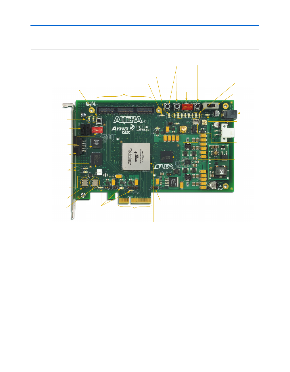
Figure 2–1 shows the Arria GX development board.
Switch
(S1, S2, S4)
Figure 2–1. Arria GX Development Board
Configuration
Push Button (S5)
Channel Activity
LEDs (D12 and D13)
JTAG Chain Bypass
Switches for the
MAX II Device and
the HSMC (SW2, SW3)
Configuration
DIP Switch (S6)
JTAG Header (J6)
MAX II CPLD (U5)
PCIe Power
Mode LEDs
(D19 and D20)
Flash Device (U6)
Oscillator (X2)
Oscillator (X3)
125 MHz
62.5 MHz
Voltage Present LEDs
(D21, D22, D23)
HSMC Present LED (D1)
HSMC Connector (J2)
PCIe Edge
Connector (J14)
Configuration
Done LED
(D2)
PCIe Mode
Select Jumper (J13)
es
User DIP
Switch (S3)
DDR2 SDRAM (U8)
Getting Started
User LEDs
(D3 through D10)
Powe r
Switch (SW1)
DC Power
Jack (J1)
Powe r
LED (D11)
100 MHz
Oscillator (X1)
SMA Clock
Input (J4)
f Refer to the Arria GX Development Board Reference Manual (available on
the Arria GX Development Kit CD-ROM) for information on the board
components.
Hardware Requirements
To run the pre-installed demo application design requires only a single
computer, Computer #1, with a x4 PCI Express slot to hold the Arria GX
development board.
For application development, however, it is best to also use a second
computer, Computer #2, that is loaded with the Quartus II software as a
programming host. This setup provides the flexibility needed for
downloading different device programming files to the development
board.
Altera Corporation Getting Started User Guide 2–3
October 2007 Arria GX Development Kit
Page 10

Software Installation
f The Quartus II software requires some minimum system requirements;
f Refer to the Quartus II Installation & Licensing for Windows document for
refer to the Altera website at
http://www.altera.com/products/software/products/quartus2web/
sof-quarwebmain.html for details.
The Arria GX Development Kit provides all of the other hardware needed
to use the board.
Software Requirements
This kit requires the following software:
■ Windows XP operating system running on both computers
■ Quartus II Web Edition software version 7.2 or later.
1 Although it is already available on the DVD included in the kit,
you can also download the Quartus II software from the Altera
website at http://www.altera.com/products/software/
products/quartus2web/sof-quarwebmain.html.
further information on the Quartus II system software requirements,
especially heeding the following:
● A web browser, Microsoft Internet Explorer version 5.0 or later
or Firefox version 2.0 or later. You need a web browser to register
the Quartus II software and request license files. Refer to
“Licensing Considerations” on page 2–7.
● Version 2.0 or later of the .NET framework. Refer to page 2–9 for
the .NET related issue.
Software
Installation
The instructions in this section explain how to install the following:
■ Arria GX Development Kit CD-ROM
■ Arria GX Development Kit demo application and drivers
■ The Quartus II Web Edition Software DVD, including MegaCore
functions from the MegaCore IP Library
Installing the Arria GX Development Kit CD-ROM Contents
Perform this installation on Computer #1.
The Arria GX Development Kit CD-ROM contains the following items:
■ Arria GX Development Kit GUI application and drivers
■ Example design programming files
2–4 Getting Started User Guide Altera Corporation
Arria GX Development Kit October 2007
Page 11

Getting Started
■ Arria GX Development Kit Getting Started User Guide (this document)
■ Arria GX Development Board Reference Manual
To install the Arria GX Development Kit CD-ROM contents, perform the
following steps:
1. Insert the Arria GX Development Kit CD-ROM into your CD-ROM
drive.
1 If the installer does not find the setup file, browse to the
CD-ROM drive and double click on the setup.exe file.
2. Follow the online instructions to complete the installation process.
The installation program copies the Arria GX Development Kit files to
your hard-disk, copies the software drivers and application, and in
Programs > Altera > Arria GX PCI Express Kit <version#> in the
Windows Start menu creates an icon , which you can use to launch the
development kit GUI.
When the installation is complete, the Arria GX Development Kit
installation program creates the directory structure shown in Figure 2–2,
where <path> is the Arria GX Development Kit installation directory.
Figure 2–2. Arria GX Development Kit Installed Directory Structure
<
path
>
The default Windows installation directory is C:\altera\
ArriaGX_PCIe
board_design_files
docs
examples
<Quartus II version number>
\kits.
Table 2–1 lists the file directory names and a description of their contents.
Table 2–1. Installed File Directory Names and Description of Contents
Directory Name Description of Contents
board_design_files Contains the board design and production test files. You can use the board design
files as a starting point for creating your own prototype board.
docs Contains documentation related to the development kit, including a directory of some
basic FPGA-related tutorials.
examples Contains the example design files for the Arria GX Development Kit.
Altera Corporation Getting Started User Guide 2–5
October 2007 Arria GX Development Kit
Page 12

Software Installation
Installing the Quartus II Software and MegaCore Functions
Perform this installation on Computer #2, or on Computer #1 if using only
one computer.
Load the Altera Complete Design Suite DVD into the DVD player, and
click on Install free package on the startup screen (Figure 2–3). Follow
the on-screen instructions and accept all defaults. After installing the
software, request and install a license to enable it.
f For information on obtaining a license file, refer to “Licensing
Considerations” on page 2–7.
1 During installation of the Quartus II software, choose to install
the MegaCore IP Library when presented the option and follow
the on-screen instructions.
Figure 2–3. Quartus II Installation from DVD
2–6 Getting Started User Guide Altera Corporation
Arria GX Development Kit October 2007
Page 13

Getting Started
Licensing Considerations
Using the Demo Application and Example Design
Before using the Quartus II software, you must request a license file from
the Altera web site at www.altera.com/licensing and install it on your
computer. When you request a license file, Altera emails you a license.dat
file that enables the software.
1 To license the Quartus II software, you need your network
interface card (NIC) ID, a 12-digit hexadecimal number that
identifies your computer. Networked (or floating-node)
licensing requires a NIC ID or server host ID. When obtaining a
license file for network licensing, use the NIC ID from the
computer that will issue the Quartus II licenses to distributed
users over a network. You can find the NIC ID for your card by
typing "ipconfig /all" at a command prompt. Your NIC ID
is the number on the physical address line, without the dashes.
The kit provides an example design file and an easy-to-use demo
application with a custom GUI. Using the demo application GUI you can:
■ Specify endpoint (PCI Express x4 MegaCore function) read, write,
and loop commands
■ Specify memory read/write and loop commands
■ Read various configuration registers
In this section, you perform the following tasks:
■ Install the demo application drivers
■ Install the Arria GX development board
■ Perform memory read and write transactions on the board
1 The Arria GX development board ships with a pre-installed
example design. For instructions on installing the example
design or any other design to the flash memory on the board,
refer to Appendix A, Programming the Development Board.
Data Flow Block Diagram
Figure 2–4 shows a block diagram of the data flow from the x4 PCI
Express edge connector through the Arria GX device block, which
includes the application layer, Altera PCI Express x4 MegaCore function,
and the Quartus II software alt2gxb megafunction.
The kit’s demo application allows for memory read and write
transactions to the development board. In addition, the kit’s example
design (AGX_PCIe_Example_Design.sof) has a DMA engine that allows
the development board to write to on-chip memory.
Altera Corporation Getting Started User Guide 2–7
October 2007 Arria GX Development Kit
Page 14

Using the Demo Application and Example Design
r
Figure 2–4. Arria GX Device Block
Target
Memory
Application Layer
Target
Memory
Control
DMA
Registers
DMA
Engine
Altera PCI Express
x4 MegaCore
Function
Arria GX Device
Quartus II Software
alt2gxb Megafunction
Install Drivers and Arria GX Development Board
As stated in the “Hardware Requirements” on page 2–3, for a flexible
setup that allows you to download different programming files to the
on-board Arria GX device, Altera recommends that you use two
computers: Computer #1 as the development board host computer, and
Computer #2 as the Quartus II programming host computer.
x4 PCI Express
Edge Connecto
f This section discusses the example design and the development board
host computer (Computer #1). For information on using the Quartus II
programming host computer (Computer #2), refer to Appendix A,
Programming the Development Board.
To install the demo application drivers and Arria GX development board,
use the following steps:
1 To install the drivers, you need to have administrator privileges
on your computer.
From Computer #1:
1. Install the Arria GX Development Kit CD-ROM.
2–8 Getting Started User Guide Altera Corporation
Arria GX Development Kit October 2007
Page 15

Getting Started
2. Open the ..examples\Getting_Started\Software
Application\JungoDrivers directory, and double-click the
install.bat file.
3. After the install.bat file finishes copying files and installing the
drivers, shut down Computer #1.
4. Ensure that the Power slide switch is in the OFF position on the
Arria GX development board and insert the board into a x4 (or
wider) PCI Express slot.
Finish Installing the Drivers and the Development Board
Finish installing the demo application drivers and the Arria GX
development board by performing the following steps:
1 If you want to download a programming file that is different
than the kit’s pre-installed example design file, refer to
Appendix A, Programming the Development Board.
1. Start Computer #1.
2. When the Windows XP Found New Hardware Wizard appears,
click Next.
3. When the Hardware Installation dialog box appears, click
Continue Anyway.
4. Click Finish in the Completing the Found New Hardware Wizard
to finish installing the drivers.
Run the Demo Application
Run the demo application by performing the following steps:
1. To start the demo application GUI, execute the altpcie_demo.exe
file found in the <path>
\ArriaGX_PCIe\examples\Getting_Started\Software
Application directory.
1 If you receive an “Application Error” message when
launching the demo application, please install version 2.0 or
later versions of the .NET framework. Some Windows versions
do not have runtime DLL for the .NET application. The .NET
framework application can be downloaded from the following
location: http://www.microsoft.com/download.
2. Configure the parameters in the Altera PCI Express
High-Performance Demo Application (Figure 2–5) as follows:
Altera Corporation Getting Started User Guide 2–9
October 2007 Arria GX Development Kit
Page 16

Using the Demo Application and Example Design
● Confirm Transfer length (bytes) is 100000
● Confirm Sequence is Write only
● Confirm Number of iterations is 10
● Confirm Arria GX board is selected.
3. Click Run. A message appears indicating the transfer speed for the
selected operational sequence.
f You can configure the demo kit application to perform other tests
including various memory read and write transactions on the board.
Figure 2–5. Altera PCI Express High-Performance Demo Application
2–10 Getting Started User Guide Altera Corporation
Arria GX Development Kit October 2007
Page 17

Getting Started
Using the Arria GX Development Board for Your Applications
You can use the Arria GX development board to develop PCI Express as
well as other applications.
PCI Express Applications
As you develop the application, at some point you program the FPGA
with your design by downloading programming files to the development
board. You can use the following programming methods:
■ By SRAM Object File (SOF)
With this method, you download an SOF directly into the FPGA with
the development board installed in Computer #1. This method is
faster to make changes and debug your application. One
disadvantage of this method is that it requires a second computer.
Another disadvantage is that the FPGA does not retain the
downloaded programming file after the board is powered down.
■ By Programmer Object File (POF)
With this method, you download a POF to the on-board flash device.
The advantage for this method is that whenever the development
board powers up, the flash device configures the FPGA. Production
systems can use this method of programming because the flash
device would load the application when the shipped product
powers up at the customer site.
SOF Programming
For SOF programming, perform the following steps:
1. With Computer #1 powered off, install the Arria GX development
board into an open PCI Express slot.
2. Plug the external power supply into the DC Power Input (J1) on the
development board.
3. Insert the 10-pin female USB-Blaster plug into the JTAG Header (J6)
visible through the bracket on the side of the board.
4. Connect the USB cable between the USB-Blaster device and
Computer #2, the computer that you will use to program the FPGA.
1 Ensure that Computer #2 already has the Quartus II software
loaded and licensed and the USB-Blaster drivers installed.
Altera Corporation Getting Started User Guide 2–11
October 2007 Arria GX Development Kit
Page 18

Using the Arria GX Development Board for Your Applications
5. Slide the power switch (SW1) on the development board to ON to
power up the board.
6. From the Quartus II Programmer running on Computer #2,
download the SOF containing your application to the FPGA on the
Arria GX development board.
7. Turn on Computer #1.
1 You may remove the external power supply from the Arria GX
development board at this point. However, it is not necessary,
because the on-board power multiplexer circuit disconnects the
external power source when it detects power provided by the
computer through the PCI Express bus.
POF Programming
To use the POF programming method, follow the directions described in
Appendix A to program the flash device on the Arria GX development
board with your application. Then perform the following steps:
1. With Computer #1 powered off, install the Arria GX development
board into an open PCI Express slot.
2. Power up Computer #1 to load your application from the flash
device into the FPGA. If your PCI Express application performs
correctly, then the Arria GX development board is ready to
communicate over the PCI Express bus of Computer #1.
Non-PCI Express Applications
When developing a non-PCI Express design, remove the board from
Computer #1, install the stand-off support pegs, connect the provided
separate power supply, and run any experiments in this stand-alone
configuration using SOF or POF programming.
2–12 Getting Started User Guide Altera Corporation
Arria GX Development Kit October 2007
Page 19

Appendix A. Programming the
Development Board
Introduction
Hardware Setup
This appendix describes the method for programming the development
board when using the board for application development.
Chapter 2, Getting Started, describes the procedure for starting up and
running a pre-installed example design using Computer #1, the
development board host computer. You can also use this computer for
application development, but it involves a cumbersome process because
it requires repeatedly powering down and restarting the computer as
well as removing and reinserting the development board.
Therefore, for application development, Altera recommends that along
with the development board host computer, Computer #1, you also use a
second computer, Computer #2, as the Quartus II programming host and
as a parallel flash loader (PFL). From Computer #2, you can download a
programming file to the development board that is different from the kit’s
pre-installed example design file.
This appendix guides you through the following tasks:
■ Installing the Altera PFL provided for flash memory programming
and FPGA configuration.
■ Using the PFL to write your application to the flash device, which
then configures the FPGA.
Altera provides a USB-Blaster cable with the kit. You need this cable for
the PFL to download an application to the on-board flash device. Prepare
the Arria GX development board for downloading by performing the
following steps:
1. Connect the 10-pin female plug of the USB-Blaster cable to the
10-pin male JTAG header (J6) visible through the bracket on the side
of the development board.
2. Connect the other end of the USB-Blaster cable to the USB port of
the computer running the Quartus II software.
3. Connect the 16 V power supply, provided in the kit, to the DC
power input (J1) on the development board and to a power source.
4. Set the power switch (SW1) to ON to power up the Arria GX
development board.
Altera Corporation Getting Started User Guide A–1
October 2007 Arria GX Development Kit
Page 20

Using the Parallel Flash Loader
Using the
Parallel Flash
Loader
This section describes how to use the PFL to load an FPGA image into the
Common Flash memory Interface (CFI) type flash device and configure
the Arria GX type FPGA device on the Arria GX development board.
First, you use the Quartus II development tool to prepare and program
the MAX
loader. At the same time, you prepare and download an application to the
flash device on the board. Finally, using the flash data, the PFL configures
the FPGA and activates the application.
The tutorial uses two files included with the development kit under
Getting Started\Programming Files on the CD-ROM:
■ pfl_3fe.pof, which is the MAX II POF that contains a parallel flash
■ MyFirstFPGA.sof, which contains a simple test design that forces
The tutorial contains three parts:
■ Launch the Quartus II Development Tool
■ Prepare Application File for Downloading
■ Set Up the Programming Download
®
II device on the development board with the parallel flash
loader design.
the FPGA to display counting on the development board user LEDs.
The MyFirstFPGA.sof file is used in the SOF-to-POF conversion in
the “Prepare Application File for Downloading” part of the tutorial.
A–2 Getting Started User Guide Altera Corporation
Arria GX Development Kit October 2007
Page 21

Launch the Quartus II Development Tool
Start the Quartus II software (Figure A–1).
Figure A–1. Quartus II Software Interface
Prepare Application File for Downloading
To prepare the example application for downloading to the flash device,
convert MyFirstFPGA.sof to a POF.
To convert an SOF to a POF, perform the following steps:
1. On the File menu, click Convert Programming Files.
2. Under Output Programming File (Figure A–2) select Programmer
Object File (.pof) in the Programming file type box.
Altera Corporation Getting Started User Guide A–3
October 2007 Arria GX Development Kit
Page 22

Using the Parallel Flash Loader
Figure A–2. Convert Programming Files Options
3. Select CFI_512MB as the flash size in the Configuration device box
and set the mode in the Mode box to Fast Passive Parallel.
4. In the File name box, specify a file name for the resulting CFI flash
POF. In this example, use
C:\altera\72\kits\ArriaGX_PCIe\examples\Getting_Started\
Programming Files\MyFirstFPGA.pof.
A–4 Getting Started User Guide Altera Corporation
Arria GX Development Kit October 2007
Page 23

5. Click Options and set the option bit start address to 0x03FE0000
(Figure A–3), then click OK. This address must match the option bit
address location specified in the PFL MegaWizard
Figure A–3. Options Dialog Box
6. Under Input files to convert, click on the SOF Data cell, then click
Add File. Browse to the directory Examples\MyFirstFPGA,
highlight the MyFirstFPGA.sof file, and click Open. This adds
MyFirstFPGA.sof to the Input files to convert list (Figure A–4).
Figure A–4. Setting Input Files to Convert
®
interface.
7. Confirm that the Convert Programming Files dialog box appears
with the selections shown in Figure A–5.
Altera Corporation Getting Started User Guide A–5
October 2007 Arria GX Development Kit
Page 24

Using the Parallel Flash Loader
Figure A–5. Convert Programming Files Selections
8. Click on MyFirstFPGA.sof to highlight it, then click the Properties
button.
9. In the SOF File Properties dialog box, select Compression and click
OK to close the box.
10. Click Generate to produce the POF that you will store in the flash
device with the PFL.
A–6 Getting Started User Guide Altera Corporation
Arria GX Development Kit October 2007
Page 25

Set Up the Programming Download
If you are using two computers for application development, then start
this procedure with step 7. Otherwise, if you are using just one computer,
you must first prepare the hardware as follows:
1. Turn off Computer #1 and remove the development board from the
PCI Express slot.
2. Connect the board to the power supply provided in the kit.
3. Turn the on-board power supply switch to the ON position.
4. Power up the board.
5. Connect the USB-Blaster cable between the board and Computer #1,
now used as the Quartus II programming host computer.
6. Follow the tutorial steps to program the flash memory, starting with
step 7. After completion of all programming steps:
a. Power down the board, remove the power supply, and set the
power supply switch to OFF.
b. Power down the computer and disconnect the USB-Blaster
cable at both ends.
c. Reinsert the board into the PCI Express slot in Computer #1 and
turn the computer ON.
7. To open the programmer, click on Programmer in the Tools menu.
8. Click the Hardware Setup button.
9. In the Hardware Setup dialog box (Figure A–6), select the
download cable you are using. In this example, in the Currently
selected hardware box, select USB-Blaster and click Close.
Altera Corporation Getting Started User Guide A–7
October 2007 Arria GX Development Kit
Page 26

Using the Parallel Flash Loader
Figure A–6. Hardware Setup Selections
10. Click Auto Detect and, in the displayed JTAG chain (Figure A–7),
verify the correct setup: the EPM570 MAX II device, the CFI_512MB
flash chip, and the Arria GX FPGA, EP1AGX50CF484C6N. You will
program the MAX II device and the flash chip with a POF.
1 You may have to press the CONFIG push-button switch
(S5) on the board during this process before the flash chip
appears in the chain.
Figure A–7. JTAG Chain
A–8 Getting Started User Guide Altera Corporation
Arria GX Development Kit October 2007
Page 27

11. Click on the EPM570 device to highlight it, then right-click it and
select Change File to select a file.
12. Find and select the pfl_3fe.pof file in the Programming Files
directory, and click Open. The pfl_3fe.pof file defines the PFL
design for the MAX II device, shown as EPM570F100 in Figure A–8.
Figure A–8. Open the PFL Design File
13. If the CFI_512MB flash device is listed under the EPM570F100
device as shown in Figure A–8, go to step 15. Otherwise, highlight,
then right-click pfl_3fe.pof in the Programmer, then click the Attach
Flash Device option.
14. Highlight and check CFI_512MB (Figure A–9) and click OK.
Altera Corporation Getting Started User Guide A–9
October 2007 Arria GX Development Kit
Page 28

Using the Parallel Flash Loader
Figure A–9. Selecting the Flash Device Size
15. Right-click CFI_512MB and select Change File. Browse to the
location of the POF generated during the SOF-to-POF conversion
and click Open. This step attaches the flash POF to the MAX II POF.
16. Turn on the check boxes for Program/Configure next to the
pfl_3fe.pof items CFM, UFM, Page_0, and OPTION_BITS
(Figure A–10). Also turn on the check boxes for Verify next to
Page_0 and OPTION_BITS.
Figure A–10. Program/Configure Check Boxes
A–10 Getting Started User Guide Altera Corporation
Arria GX Development Kit October 2007
Page 29

Figure A–11. Error Message
17. Click Start to program the PFL into the MAX II device as well as
program the flash device with the FPGA image. After programming
is completed, the PFL configures the FPGA with the data from the
flash device. When completed, the application loaded into the
FPGA causes the USER_LED[7..0] lights to display counting.
1 If the FPGA is already configured prior to performing the
previous steps, the following message may appear in the
Message Window:
Info: Device 1 silicon ID is not ready - waiting
for pfl_flash_access_granted to be asserted
Figure A–11 shows the error message. In this case, press the
CONFIG push-button switch on the board to reset the FPGA.
Operation resumes, allowing the PFL to access the flash device
for programming.
18. After the PFL loads the application to the FPGA, the application
program activates and the LEDs on the board display counting. If
you cycle the power switch, the program reloads from the flash
device to the FPGA.
1 To reconfigure the board for PCI Express experiments, repeat
this procedure using top_x4_comp_3fe.pof as the flash POF.
Altera Corporation Getting Started User Guide A–11
October 2007 Arria GX Development Kit
Page 30

Using the Parallel Flash Loader
A–12 Getting Started User Guide Altera Corporation
Arria GX Development Kit October 2007
Page 31

Additional Information
Revision History
Chapter Date Version Changes Made
All October 2007 7.2.0 First publication
How to Contact
The table below displays the revision history for the chapters in this user
guide.
For the most up-to-date information about Altera products, refer to the
following table.
Altera
Contact (1)
Technical support Website www.altera.com/support
Technical training Website www.altera.com/training
Product literature Website www.altera.com/literature
Altera literature services Email literature@altera.com
Non-technical support (General)
(Software Licensing)
Note to table:
(1) You can also contact your local Altera sales office or sales representative.
Contact
Method
Email custrain@altera.com
Email nacomp@altera.com
Email authorization@altera.com
Address
Typographic
This document uses the typographic conventions shown below.
Conventions
Visual Cue Meaning
Bold Type with Initial
Capital Letters
bold type External timing parameters, directory names, project names, disk drive names,
Italic Type with Initial Capital
Letters
Altera Corporation Info–i
Command names, dialog box titles, checkbox options, and dialog box options are
shown in bold, initial capital letters. Example: Save As dialog box.
filenames, filename extensions, and software utility names are shown in bold
type. Examples: \qdesigns directory, d: drive, chiptrip.gdf file.
Document titles are shown in italic type with initial capital letters. Example: AN
75: High-Speed Board Design.
Preliminary
Page 32

Typographic Conventions Stratix II GX EP2GX90 Signal Integrity Development Board Reference Manual
Visual Cue Meaning
Italic type Internal timing parameters and variables are shown in italic type.
Examples: t
Variable names are enclosed in angle brackets (< >) and shown in italic type.
Example: <file name>, <project name>.pof file.
Initial Capital Letters Keyboard keys and menu names are shown with initial capital letters. Examples:
Delete key, the Options menu.
“Subheading Title” References to sections within a document and titles of on-line help topics are
shown in quotation marks. Example: “Typographic Conventions.”
PIA
, n + 1.
Courier type Signal and port names are shown in lowercase Courier type. Examples: data1,
tdi, input. Active-low signals are denoted by suffix n, e.g., resetn.
Anything that must be typed exactly as it appears is shown in Courier type. For
example:
actual file, such as a Report File, references to parts of files (e.g., the AHDL
keyword
Courier.
1., 2., 3., and
a., b., c., etc.
● • Bullets are used in a list of items when the sequence of the items is not important.
■
v The checkmark indicates a procedure that consists of one step only.
1 The hand points to information that requires special attention.
c
w
r The angled arrow indicates you should press the Enter key.
f The feet direct you to more information on a particular topic.
Numbered steps are used in a list of items when the sequence of the items is
important, such as the steps listed in a procedure.
The caution indicates required information that needs special consideration and
understanding and should be read prior to starting or continuing with the
procedure or process.
The warning indicates information that should be read prior to starting or
continuing the procedure or processes
c:\qdesigns\tutorial\chiptrip.gdf. Also, sections of an
SUBDESIGN), as well as logic function names (e.g., TRI) are shown in
Info–ii Altera Corporation
Preliminary
 Loading...