

Page 1
DR-M03SX S e r v ic e M a n u a l
DR-M06TH
C O N T EN TS
SPECIFICATIONS
1) General
2) Transmitter 2 MAIN Unit 22~24
3) Receiver 2
CIRCUIT DESCRIPTION SP Unit
1) Receiver System 3
2) Transmitter System 4 Packing.. 2S
3) PLL Circuit
4) Terminal Function of Microprocessor
5) Terminal Connection of Microprocessor 8 ADJUSTMENT
SEMICONDUCTOR DATA 1) Required Test Equipment.
1) AK2341 9 2) Adjustment for DR-M06/03 28~29
2) AN78L05M 1G
3) AN8010M 1G
4) BU4052BF 1G
5) LR408721 11 CIRCUIT DIAGRAM
6) M5218FP 11 3) Main Unit 32
7) M56760FP 12 4) Main Unit 33
8) MC7808CT 13
9) RH5VA32AA-T1 13
10) RH5VA45AA-T1 13 PC BOARD VIEW
11)M57735 14
12) TK10487MTR 1S
13) AT24C02N-10SI-2.7 1S
14) AT24C08-10SI-2.7 1S
15) uPC1241H 16
16) Transistor, Diode and LED Outline Drawings 16 6) VCO Unit Side B
17) LCD Connection 17
EXPLODED VIEW
1) Bottom View
2) LCD View 18
3) Top, Front View 1
4) Top, Front View 2
5)DRM03 PA UNIT 21
VERSION TABLE
2
4 DRM03 PA Unit 2S
S ~ 7
18
19
2G
21
A L IN C O IN C O R P O R A T E D
TWIN 21 M.I.D. TOWER BUILDING 23F, 1-61, 2-CHOME,
SHIROMI CHUO-KU , OSAKA, 540-8580 JAPAN
PARTS LAST
CPU Unit
VCO Unit
Mechanical Parts
3) Adjustment Points
4) Adjustment Quick Reference
5) CPU Unit
1) Main Unit Side A
2) Main Unit Side B
3) CPU Unit Side A.
4) CPU Unit Side B
5) VCO Unit Side A
22
24
2S
2S
27
3G
3G
34
3S
36
37
37
38
38
Tel (81)6-6946-8150 fax (81)6-6946-8175
e-mail: export@alinco.co.jp
Page 2
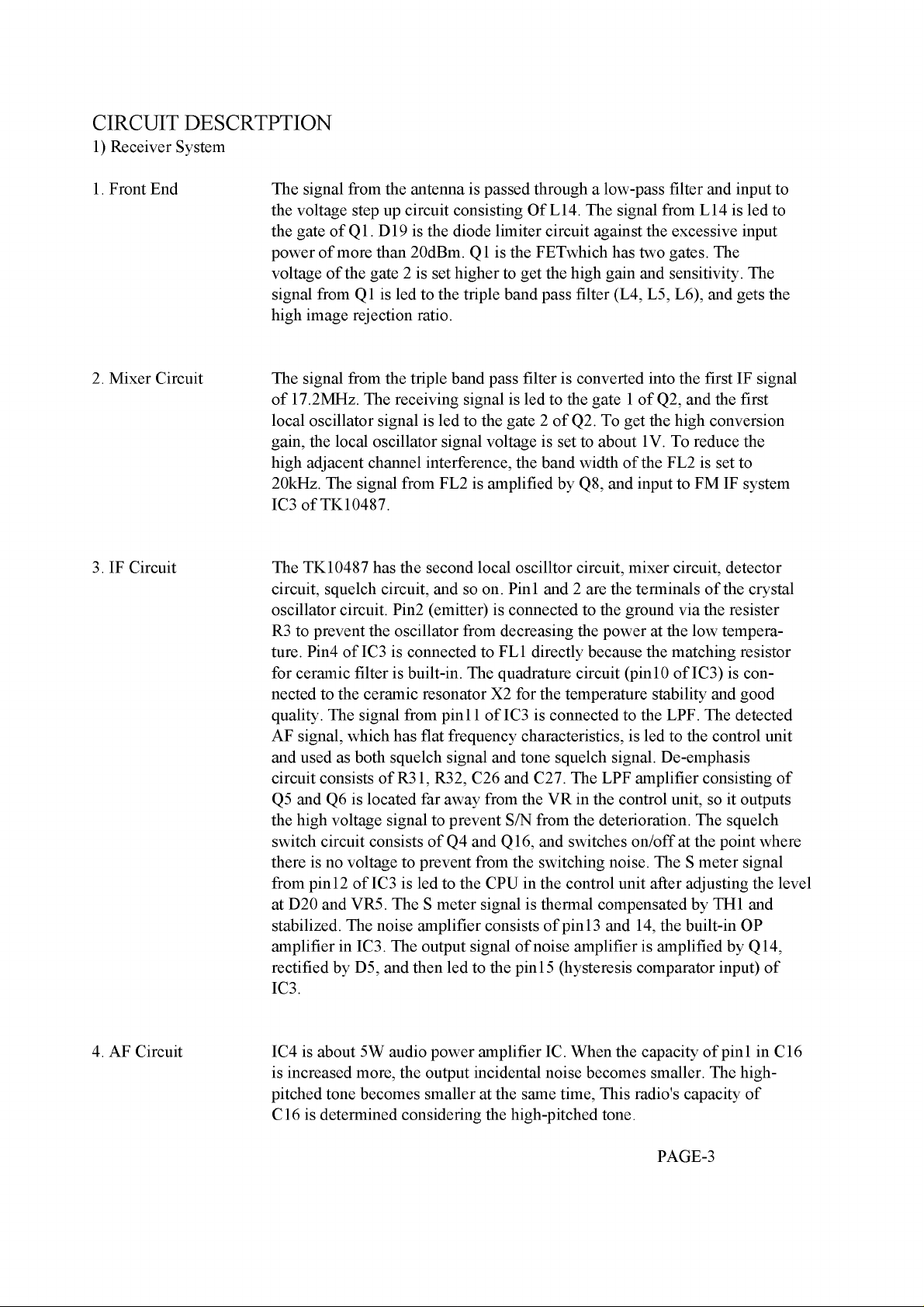
* S PEC IF IC A TIO N S
GENERAL
Frequency
DRM03SX
DRM06TH
28.00 - 29.700MHz
50.00 - 54.00MHz
Step
Channel
Modulation
Antenna impedance
Power supply
Current
Dimensions
Weight
Transmitter
Power output
Modulation
Max deviation
Spurious
Microphone
Operatin Mode
Offset
Receiver
Receiver sys
I.F.
Sensitivity
Selectivity
AF Output
5 , 10 , 12.5 , 15 , 20 , 25 KHz selectable
100
F3E (FM)
50 ohm unbalanced
13.8V DC +/- 10%
Tx high.approxl 3.0a (DRM03SX)
Rx squelched.less than 600mA
DRM03SX 140(W) x 40(H) x 115(D)
DRM06TH 140(W) x 40(H) x 155(D)
DRM03SX approx 681gs
DRM06TH approx 800gs
DRM03SX High : 10W Low: 1W
DRM06TH High : 20W Low: 2W
variable reactance frequency modulation
+/- 5.0kHz
-60dB or under below carrier
Electret Condenser Microphone
Simplex/Semi-Duplex
0 to +/-15.995MHz freely programmable
Double-conversion superheterodyne
10.7MHz and 455kHz
DRM03SX 0.16uV (-16dBu) 12dB SINAD
DRM06DX 0.25uV (-12dBu) 12dB SINAD
+/- 6kHz or under at -6dB
+/- 15kHz or under at -60dB
2.5W with 8ohm at 10%distortion
8ohm
Page 2
Page 3
C IR C U IT D E S C R T P T IO N
1) Receiver System
1. Front End
2. Mixer Circuit
3. IF Circuit
The signal from the antenna is passed through a low-pass filter and input to
the voltage step up circuit consisting Of L14. The signal from L14 is led to
the gate of Q1. D19 is the diode limiter circuit against the excessive input
power of more than 20dBm. Q1 is the FETwhich has two gates. The
voltage of the gate 2 is set higher to get the high gain and sensitivity. The
signal from Q1 is led to the triple band pass filter (L4, L5, L6), and gets the
high image rejection ratio.
The signal from the triple band pass filter is converted into the first IF signal
of 17.2MHz. The receiving signal is led to the gate 1 of Q2, and the first
local oscillator signal is led to the gate 2 of Q2. To get the high conversion
gain, the local oscillator signal voltage is set to about 1V. To reduce the
high adjacent channel interference, the band width of the FL2 is set to
20kHz. The signal from FL2 is amplified by Q8, and input to FM IF system
IC3 of TK10487.
The TK10487 has the second local oscilltor circuit, mixer circuit, detector
circuit, squelch circuit, and so on. Pin1 and 2 are the terminals of the crystal
oscillator circuit. Pin2 (emitter) is connected to the ground via the resister
R3 to prevent the oscillator from decreasing the power at the low tempera
ture. Pin4 of IC3 is connected to FL1 directly because the matching resistor
for ceramic filter is built-in. The quadrature circuit (pin10 of IC3) is con
nected to the ceramic resonator X2 for the temperature stability and good
quality. The signal from pin11 of IC3 is connected to the LPF. The detected
AF signal, which has flat frequency characteristics, is led to the control unit
and used as both squelch signal and tone squelch signal. De-emphasis
circuit consists of R31, R32, C26 and C27. The LPF amplifier consisting of
Q5 and Q6 is located far away from the VR in the control unit, so it outputs
the high voltage signal to prevent S/N from the deterioration. The squelch
switch circuit consists of Q4 and Q16, and switches on/off at the point where
there is no voltage to prevent from the switching noise. The S meter signal
from pin12 of IC3 is led to the CPU in the control unit after adjusting the level
at D20 and VR5. The S meter signal is thermal compensated by TH1 and
stabilized. The noise amplifier consists of pin13 and 14, the built-in OP
amplifier in IC3. The output signal of noise amplifier is amplified by Q14,
rectified by D5, and then led to the pin15 (hysteresis comparator input) of
IC3.
4. AF Circuit
IC4 is about 5W audio power amplifier IC. When the capacity of pin1 in C16
is increased more, the output incidental noise becomes smaller. The high-
pitched tone becomes smaller at the same time, This radio's capacity of
C16 is determined considering the high-pitched tone.
PAGE-3
Page 4
2) Transmitter System
1. Modulation Circuit
The microphone amplifier IC1 (IDC, LPF) consists of two operational amplifi
ers. The signal from the microphone is led to pre-emphasis circuit consisting
of C36 and R47 and then to the limiter circuit. The limiter circuit uses the
saturation of the OP amplifier. The amplified signal is input to the low-pass
filter IC1A. The output signal from the microphone amplifier is passed
through variable resistors VR2 for modulatlon adjustment and input to the
VCO unit. Sub tone deviation is determined by R24, R25 and VR2. The
radio does not have the adjustment variable resistor for sub tone deviation.
2. TX Amp. Circuit
The signal from VCO is ampriied by TX, RX wide band LO amplifier Q19.
The signal from Q19 is passed through the transmission/reception selector,
and amplified byQ20 and Q15. The PA unit is driven at 200mW driving
power.
3. PA Circuit
IC5 is 20W(M06DX) powered amplifier module. The output power is controlled by
the voltage of V1. The RF signal amplified 20W in PA is passed through D3
and three-stage transmission/reception low-pass filter, and input to the
antenna connector.
4. ALC Circuit (M06DX)
The power detection circuit consisting of D17 and D18 rectifies the output
signal voltage. The detected DC voltage is led to the VR1 (power adjust
trimmer), and amplified by Q3, Q9 and Q13. Output power is controlled by
voltage of V1 in IC5 and collector voltage of Q15. When the temperature
goes up unusually, the power down circuit consisting of R101 and TH2
works to prevent the device from the destruction.
3)P L L C ircuit (M06DX)
The VCO unit is designed for the PLL circuit, putting the VCO on one side,
and PLL circuit on the other side.
Q301 in the VCO is grounded using the gate oscmator, and its frequency
covers 50MHz to 54MHz without transmission/reception shift circuit.
IC301 is pulse swallow system based PLL IC with the built-in prescaler,
which synthesizes 150MHz-band signal.
The loop filter consisting of Q302 and Q303 is the active type.
PAGE-4
Page 5
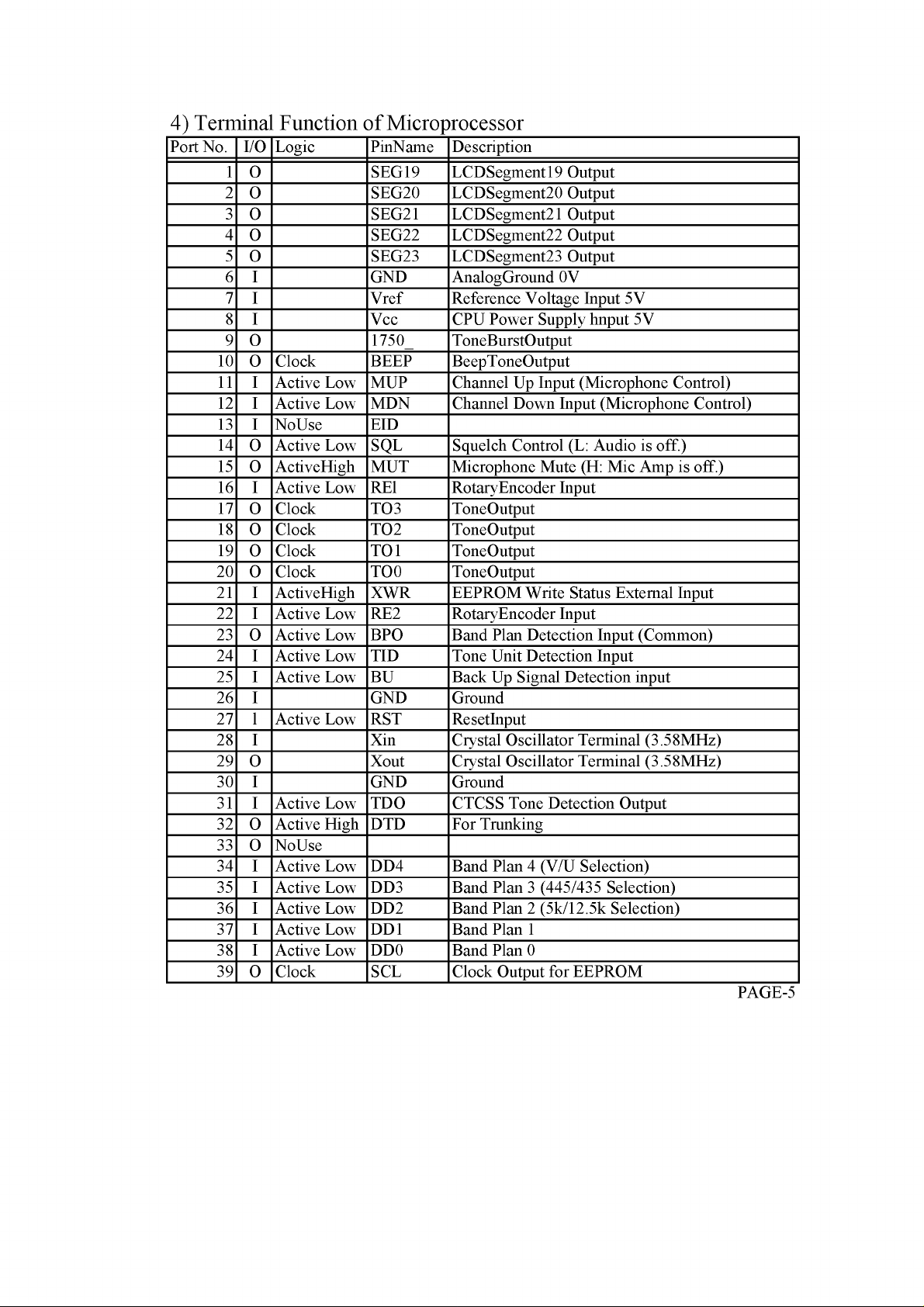
4) T e rm in al F u n ctio n o f M ic rop ro c e sso r
Port No. I/O Logic PinName
1
O SEG19
2
O
3
O
4
O
5
O
6 I
7 I
8 I
9
O
10
O Clock
11 I
12 I
13 I
14
15
16 I
17
18
19
20
21 I
22 I
23
24 I
25 I
26 I
27 l
28 I Xin Crystal Oscillator Terminal (3.58MHz)
29
30 I
31 I
32
33
34 I
35 I
36 I
37 I
38 I
39
Active Low
Active Low
NoUse
O Active Low SQL Squelch Control (L: Audio is off.)
O ActiveHigh
Active Low
O Clock
O Clock
Clock
O
Clock TO0
O
ActiveHigh
Active Low
O Active Low
Active Low
Active Low BU Back Up Signal Detection input
Active Low RST ResetInput
O Xout
Active Low TDO CTCSS Tone Detection Output
O Active High
O NoUse
Active Low
Active Low
Active Low
Active Low
Active Low
O Clock
SEG20 LCDSegment20 Output
SEG21 LCDSegment21 Output
SEG22 LCDSegment22 Output
SEG23 LCDSegment23 Output
GND AnalogGround 0V
Vref Reference Voltage Input 5 V
Vcc CPU Power Supply hnput 5 V
1750
BEEP
MUP
MDN Channel Down Input (Microphone Control)
EID
MUT
REl RotaryEncoder Input
TO3
TO2
TO1 ToneOutput
XWR
RE2 RotaryEncoder Input
BPO Band Plan Detection Input (Common)
TID
GND Ground
GND Ground
DTD For Trunking
DD4 Band Plan 4 (V/U Selection)
DD3 Band Plan 3 (445/435 Selection)
DD2 Band Plan 2 (5k/12.5k Selection)
DD1 Band Plan 1
DD0 Band Plan 0
SCL Clock Output for EEPROM
Description
LCDSegment19 Output
ToneBurstOutput
BeepToneOutput
Channel Up Input (Microphone Control)
Microphone Mute (H: Mic Amp is off.)
ToneOutput
ToneOutput
ToneOutput
EEPROM Write Status External Input
Tone Unit Detection Input
Crystal Oscillator Terminal (3.58MHz)
PAGE-5
Page 6
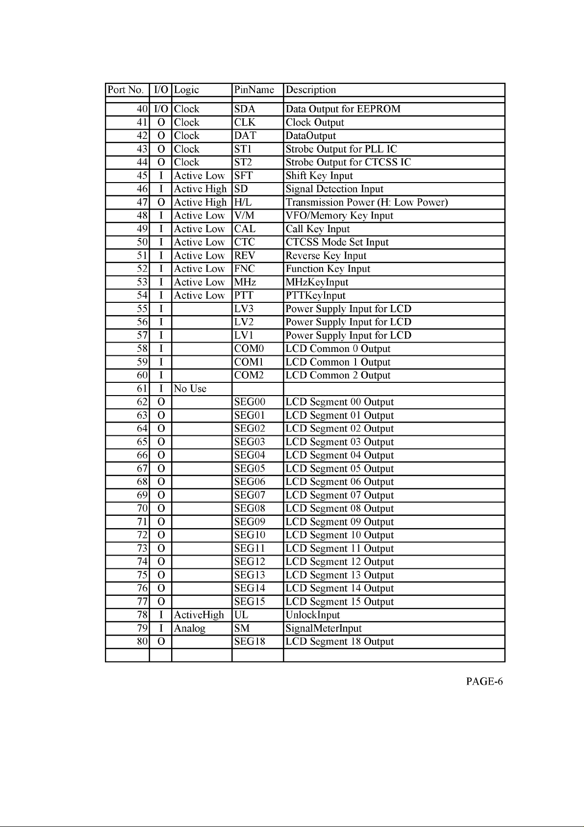
Port No. I/O Logic PinName
4G
I/O Clock SDA Data Output for EEPROM
41
O Clock
42
O Clock
43
O Clock ST1 Strobe Output for PLL IC
44
O Clock ST2 Strobe Output for CTCSS IC
4S I
46 I
47
48 I
49 I
SG I
S1 I
S2 I
S3 I
S4 I
SS I LV3
S6 I LV2
S7 I LV1
S8 I COMG LCD Common 0 Output
S9 I COM1 LCD Common 1 Output
6G I COM2 LCD Common 2 Output
61 I
62
63
64
6S
66
67
68
69
7G
71
72
73
74
7S
76
77
78 I
79 I
8G
Active Low SFT Shift Key Input
Active High SD Signal Detection Input
O Active High
Active Low V/M
Active Low
Active Low CTC CTCSS Mode Set Input
Active Low
Active Low FNC Function Key Input
Active Low
Active Low
No Use
O
O
O
O
O
O
O
O
O
O
O
O SEG11 LCD Segment 11 Output
O
O
O
O
ActiveHigh UL UnlockInput
Analog SM SignalMeterInput
O
CLK
DAT
H/L Transmission Power (H: Low Power)
CAL
REV
MHz
PTT
SEGGG
SEGG1
SEGG2
SEGG3
SEGG4
SEGGS
SEGG6
SEGG7
SEGG8
SEGG9
SEG1G
SEG12
SEG13
SEG14
SEG1S
SEG18
Description
Clock Output
DataOutput
VFO/Memory Key Input
Call Key Input
Reverse Key Input
MHzKeyInput
PTTKeyInput
Power Supply Input for LCD
Power Supply Input for LCD
Power Supply Input for LCD
LCD Segment 00 Output
LCD Segment 01 Output
LCD Segment 02 Output
LCD Segment 03 Output
LCD Segment 04 Output
LCD Segment 05 Output
LCD Segment 06 Output
LCD Segment 07 Output
LCD Segment 08 Output
LCD Segment 09 Output
LCD Segment 10 Output
LCD Segment 12 Output
LCD Segment 13 Output
LCD Segment 14 Output
LCD Segment 15 Output
LCD Segment 18 Output
PAGE-6
Page 7
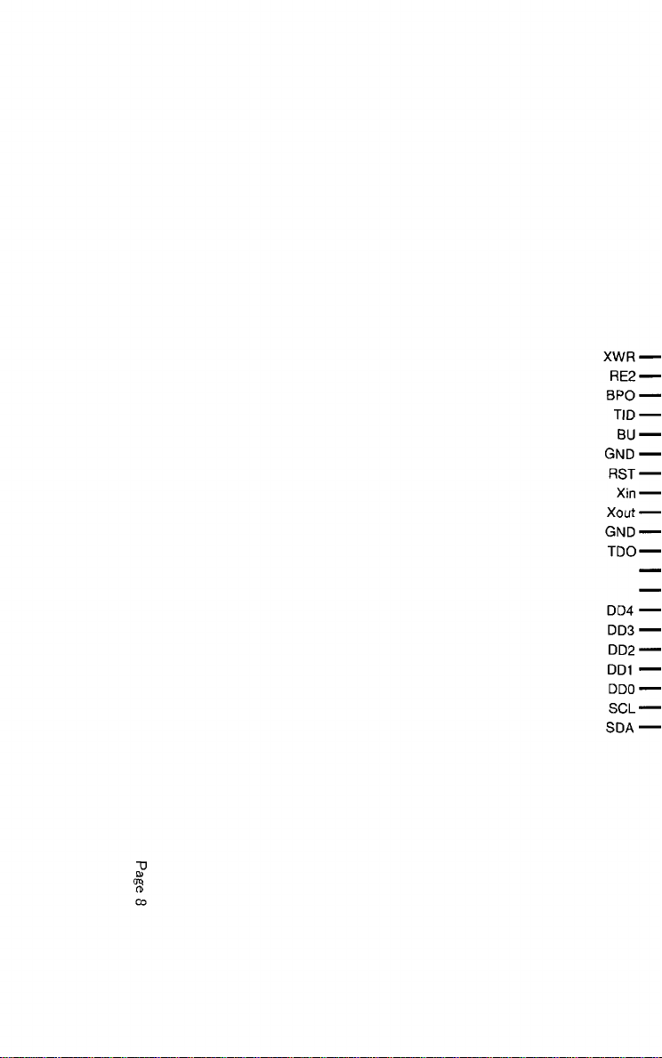
X W R
------
R E 2
------
B P O
------
TID
-----
BU
-----
G N D
------
R S T
------
Xln —
X o u t
-------
G N D
------
T D O
------
D D 4
------
D D 3
------
D D 2
------
DD1
------
D D O
------
SCL
-----
S D A -------
Page 8
Page 8
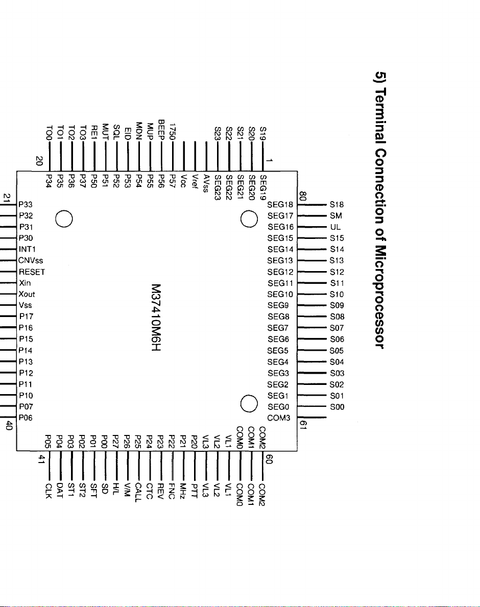
5) Terminal Connection of Microprocessor
_ 3^ CD _ l
o o o o
o -*■ ro c*>
ro
o
“0 “OTJTJ"0“0"0"0"0
QWQ Q a icnoicncn
A a i O )M O -* W W A
P 3 3 S E G 1 8
P32
P31 ^
P 3 0 SE G 1 5
IN T 1
C N V ss
R E S E T S E G 1 2
Xin
Xou t
Vss
P1 7
P 1 6
P 1 5 CD S E G 6
P1 4
P 1 3 S E G 4
P1 2 S E G 3
P1 1
P1 0
P 0 7
P0 6 C O M 3
T J X T J T J ' D ' D T J T l ' D
O O OO O O N J N JN )
cn*ui\)-‘ OMO)Oi
m C D 2 2 c m o i
- H r O Z ' D ' D O
TJ TJ
tfi tfi
cn a?
S
CO
"vl
I
TJ TJ
N> N>
.b. CO
"t 3< <>C/5 C/5C /5 C/ )C/ 5
o ^ < m m m m m
' JO ™ g Q O Q Q Q
U Tl "0 < < <
ro N> N> |— r- I-
M -*■ O 00 N> -*■
C/5 C/5 C/5 C/5 C/5
W W M IO -*
C>3 ro —*■ O CD
N> N> N> N>
O M J O O
^ S E G 1 6
s— v S E G 1
o o o
o o o
2 2 2
o —1 ro
S E G 1 7
S E G 1 4
S E G 1 3
S E G 1 1
S E G 1 0
S E G 9
S E G 8
S E G 7
S E G 5
S E G 2
SE G O
a>
o
■ S 1 8
■ SM
■ U L
■ S 1 5
■ S 1 4
• S 1 3
■ S 1 2
■ S11
■ S 1 0
■ S 0 9
• S 0 8
■ S 0 7
■ S 0 6
■S 0 5
■ S 0 4
■ S 0 3
■ S 0 2
■ S01
■ S00
O CO <Z> <Z> <Z>
o
> H h -n o
* H
X <
3) in
O N
< < < o o o
U ^ o g g
Page 9
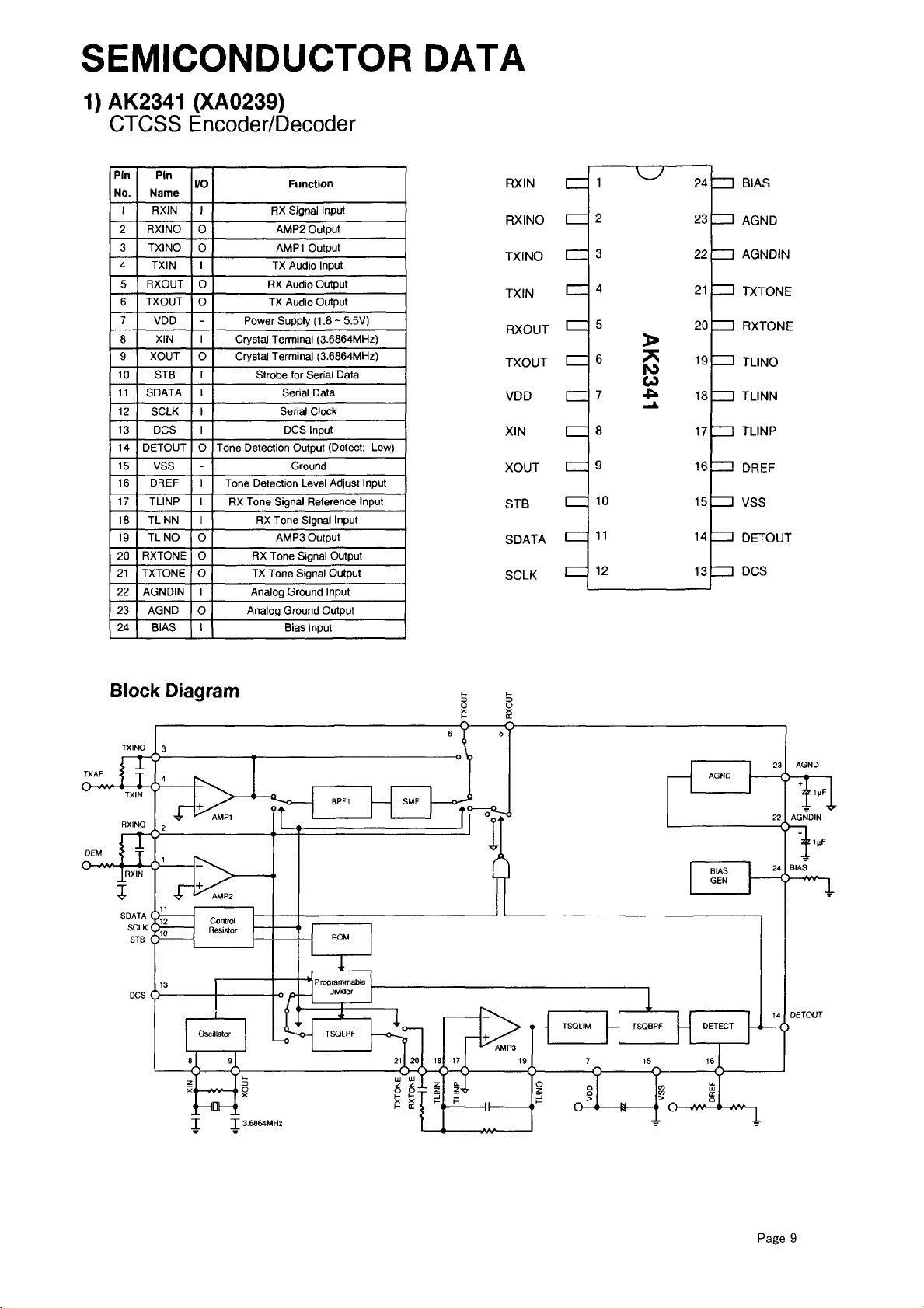
S E M IC O N D U C T O R D A T A
1) AK2341 (XA0239)
CTCSS Encoder/Decoder
Pin
Pin
Name
TXIN
VDD
XIN 1
DREF
BIAS
I/O
0
0
1
0 RX Audio Output
-
Crystal Terminal (3.6864MHz)
1
1 DCS Input
Tone Detection Output (Detect: Low)
o
-
Tone Detection Level Adjust Input
1
RX Tone Signal Reference Input
0 TX Tone Signal Output
1
0 Analog Ground Output
1
No.
1 RXIN 1
2 RXINO
3 TXINO
4
5 RXOUT
6 TXOUT o TX Audio Output
7
8
9 XOUT o Crystal Terminal (3.6864MHz)
10 STB
11 SDATA 1
12 SCLK 1
13 DCS
14 DETOUT
15 VSS
16
17 TLINP 1
18 TLINN 1 RX Tone Signal Input
19 TLINO o
20 RXTONE o RX Tone Signal Output
21 TXTONE
AGNDIN
22
AGND
23
24
Function
RX Signal Input
AMP2 Output
AMP1 Output
TX Audio Input
Power Supply (1.8 ~ 5.5V)
Strobe for Serial Data
Serial Data
Serial Clock
Ground
AMP3 Output
Analog Ground Input
Bias Input
B lo c k D ia g r a m
Page 9
Page 10
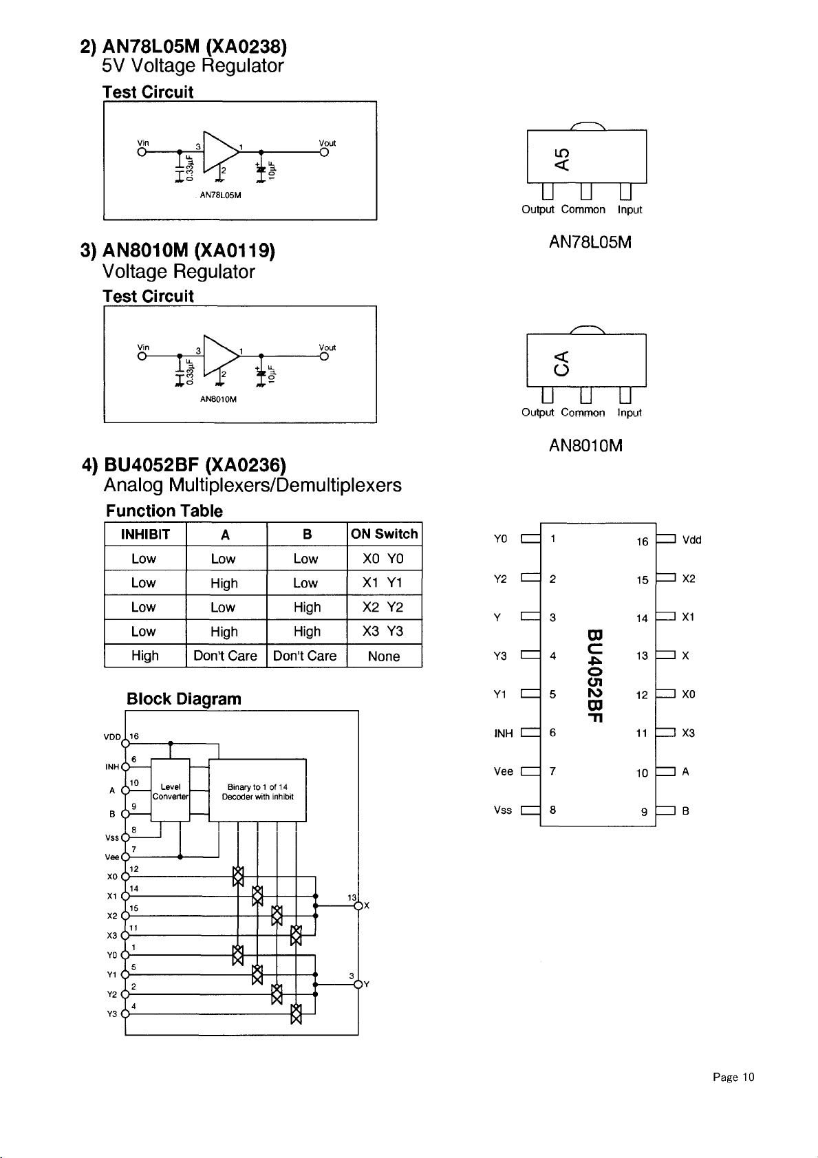
2) AN78L05M (XA0238)
5V Voltage Regulator
T e s t C i r c u i t
T T T T T T
Output Common Input
3) AN8010M (XA0119)
Voltage Regulator
T e s t C i r c u i t
4) BU4052BF (XA0236)
Analog Multiplexers/Demultiplexers
F u n c t i o n T a b le
INHIBIT
Low
Low
Low
Low
High
B lo c k D ia g r a m
High
Low High X2 Y2
High
Don't Care
A
Low Low XO YO
B
Low
High X3 Y3
Don't Care
ON Switch
X1 Y1
None
A N 7 8 L 0 5 M
n m
Output Gommon Input
A N 8 0 1 0 M
YO
Y2
Y3
Y1
INH
1
2
3
4
5
6
CD
C
-Ft
O
O l
r o
CD
T I
16
15
14
13
12
11
Vdd
X2
X1
XO
X3
Vee
Vss
7
8
10
9
Page 10
Page 11
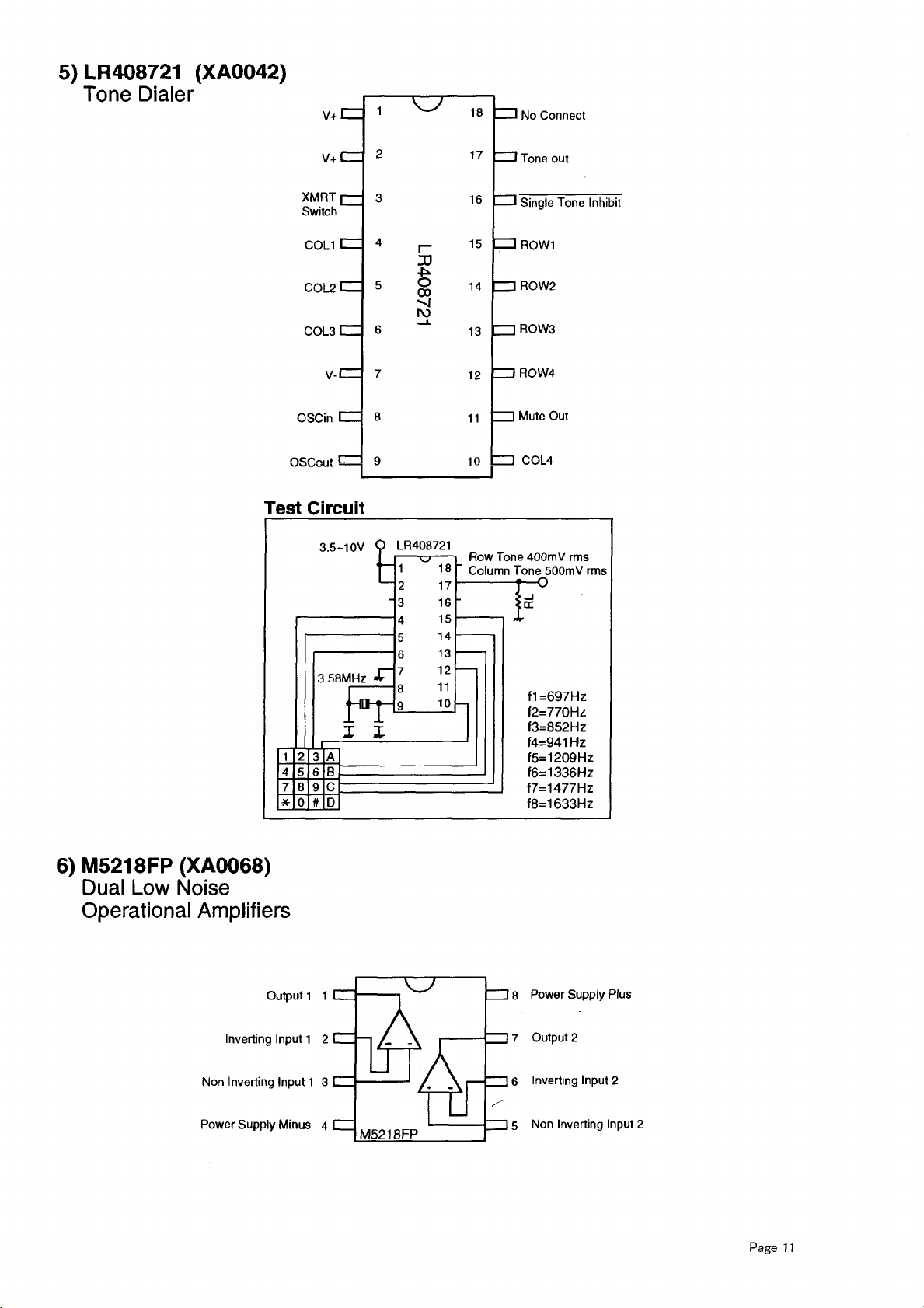
5) LR408721 (XA0042)
Tone Dialer
v+l
1 ^ 18
— 1 No Connect
v+l
XMRT [
Switch
COL1 I
COL2 I
OSCin
OSCout I
T e s t C ir c u i t
3.5-1 OV
3.58MHz
f"F
J I
2 17
3 16
4 ,— 15
JD
■P-
5 co 14
•'-J
N>
6 ~ 1 13
7 12
8 11
9 10 r z i c o L4
O LR408721
1 18
17
2
16
3
15
4
14
b
13
6
12
7
JT
11
8
10
9
— 1 Tone out
— 1 Single Tone Inhibit
Z D ROW1
-----
1 ROW2
— I ROW3
-----
1 ROW4
1 Mute Out
Row Tone 400mV rms
Column Tone 500mV rms
-O
f1=697Hz
f2=770Hz
f3=852Hz
f4=941 Hz
f5=1209Hz
f6=1336Hz
f7=1477Hz
f8=1633Hz
6) M5218FP (XA0068)
Dual Low Noise
Operational Amplifiers
Inverting Input 1 2 i —
Non Inverting Input 1 3 I
Power Supply Minus 4 I
Output 1 1
18 Power Supply Plus
17 Output 2
16 Inverting Input 2
15 Non Inverting Input 2
Page 11
Page 12
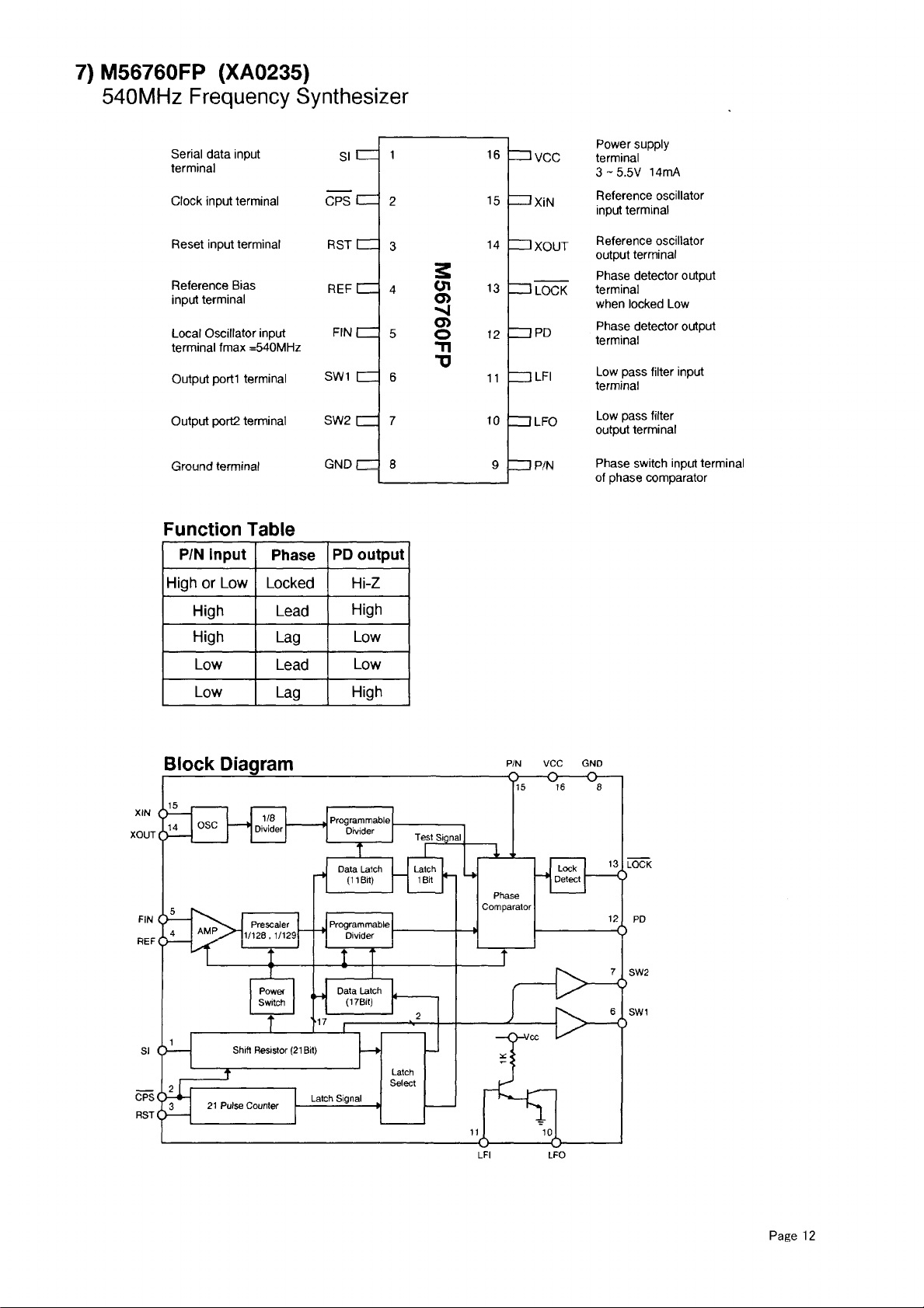
7) M56760FP (XA0235)
540MHz Frequency Synthesizer
Serial data input si I
terminal
Clock input terminal CPS I
Reset input terminal RST I
Reference Bias r e f |
input terminal
Local Oscillator input FIN I
terminal fmax =540MHz
Output portl terminal SW1 I
Output port2 terminal SW2 [
i^rnrinrt te rm inal G N D I
F u n c t i o n T a b le
P/N input
High or Low
High
High
Phase
Locked
Lead
Lag
PD output
1 16
2
3
4
5
6
7 10
8
Hi-Z
High
Low
2
O i
o>
o>
o
"n
■o
= i v c c
15
zm xiN
14
ZUXOUT
13
UNLOCK
----
IPD
12
----
1 LFI
11
IZILFO
9 IP/N
Power supply
terminal
3 -5.5 V 14mA
Reference oscillator
input terminal
Reference oscillator
output terminal
Phase detector output
terminal
when locked Low
Phase detector output
terminal
Low pass filter input
terminal
Low pass filter
output terminal
Phase switch input terminal
of phase comparator
Low
Low
Lead
Lag
Low
High
LFI LFO
Page 12
Page 13
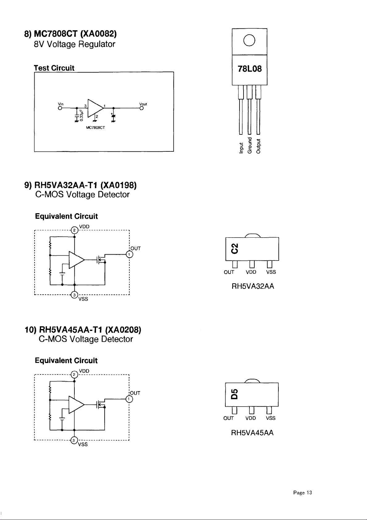
8) MC7808CT (XA0082)
8V Voltage Regulator
O
T e s t C i r c u it
9) RH5VA32AA-T1 (XA0198)
C-MOS Voltage Detector
E q u i v a le n t C i r c u i t
78L08
CM
O
10) RH5VA45AA-T1 (XA0208)
C-MOS Voltage Detector
E q u i v a le n t C i r c u it
U U □ "
OUT VDD VSS
R H 5 V A 3 2 A A
LO
Q
u u u
OUT VDD VSS
R H 5 V A 4 5 A A
Page 13
Page 14

11) M57735 (XA0271)
50~54MHz
RF Power Module
p
0 .
© V cci : 1st. DC SUPPLY
®VBB : BASE BIAS SUPPLY
@VCC2 : 2nd. DC SUPPLY
>7
T
25°C .
Tc =
2=12.5V.
Vcc i,
= 9V -
= 0.2W
Pin =
P
n
48 50 52 54 56
FREQUENCY f (M H z)
_
-
< y
O it
Page 14
Page 15

12) TK10487MTR (XA0144)
Narrow Band FM IF IC
;-------
i-
z> J
2
U.
Ct J
Vcc=3V
F=10.7MHz
Ice 5m A
Lim it 2|xV
Vo 180mV
1 . 0 %
THD
-3d B
Dev=3kHz
H W —
— CO
O o
Z
C
D
Vcc 3V
—Q
13) AT24C02N-10SI-2.7 (XA0364)
EEPROM 256 x 8Bit
14) AT24C08-1 OSI-2.7 (XA0367)
EEPROM 1024 x 8Bit
NC H Z
AO C Z
A1 C Z
NC [ZZ
A2 IZ Z
Vss I
1 14
2
3
>
H
IV
4
o
o
5
00
6
H D NC
13
IZ 3 Vcc
12
Z Z TEST
11
Z Z NC
10
Z Z SCL
9
Z Z SDA
P in N a m e s
AO ~ A2 Address inputs
SDA Serial Data
SCL Serial Clock
TEST Write Control
Vss Ground
Vcc +5V
P in N a m e s
A 0 - A 2 Address inputs
SDA Serial Data
SCL Serial Clock
TEST Hold at Vss
Vss
Vcc
Ground
+5V
NC n z
7
8
IZ ] NC
Page 15
Page 16
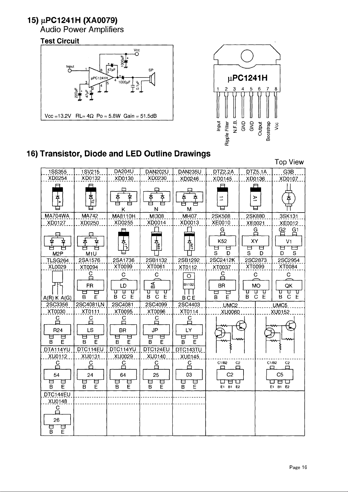
15) jllP C I 241H (XA0079)
Audio Power Amplifiers
T e s t C i r c u it
16) Transistor, Diode and LED Outline Drawings
OC
T o p V ie w
Page 16
Page 17
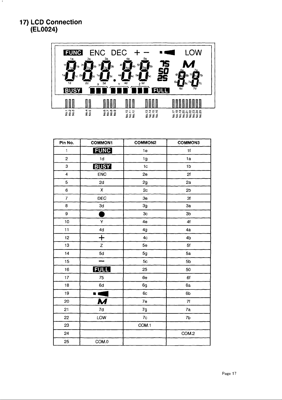
17) LCD Connection
(EL0024)
FUNC
1a 2a 3a 4a 5a
ENC DEC + - LOW
O O en ^
U L i U . L i U s s
------------------------------------------------------------------------------- O i
BUSY
T- CJ CJ
6 6 6
2 2 2
Pin Na,
1
2
3
4
5
6
7 DEC
8
9
10
11
12
13
14
15
16
17
18
19
20
21
22 LOW 7c 7b
23
24
L i
y OQ y £KJ Z
^ ID
ié
GOMMON1
f u n c H
1d
b u s y m
ENC 2e
2d
X
3d
•
Y 4e 41
4d
+
Z
5d
—
r j l H H
75
6d
■
M
7d
FU LL
co ^ in co
r,OMMnN9
1e 1f
ig
1c 1b
2g
2c
3e 3f
3g
3c 3b
4g
4c
5e
5g
5c 5b
25
6e
6g
6c 6b
7e 7f
7g
COM.1
s.ooo)o^-CNjeo^ rm
i-i-T-CJ CjW NCMOl
66 6666 666
Z Z Z Z Z Z Z Z Z
6d 7d
COMMONS
1a
2f
2a
2b
3a
4a
4b
5f
5a
50
6f
6a
7a
COM.2
25 COM.O
Page 17
Page 18
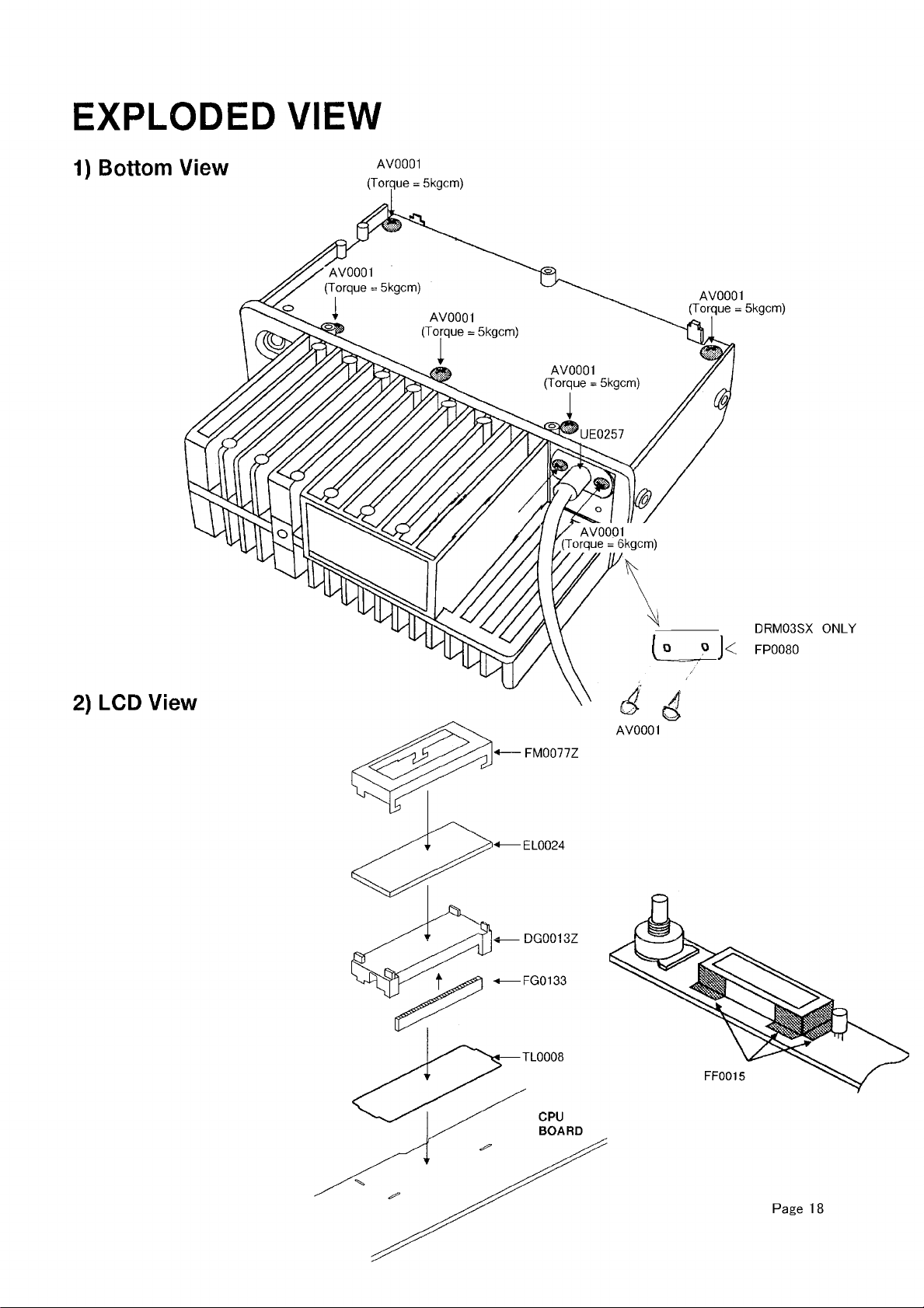
E X P L O D E D V IE W
1) Bottom View
AV0001
(Torque = 5kgcm)
AV0001
(Torque = 5kgcm)
2) LCD View
DRM03SX ONLY
Page 1 i
Page 19

3) Top, Front View 1
AE0014
(Torque = 5kgcm)
AE0014
(Torque = 5kgcm)
AE0014
(Torque = 5kgcm)
F F 0 0 2 8
K S 0 0 4 1 C Z
AE0014
(Torque = 5kgcm)
Page 19
Page 20
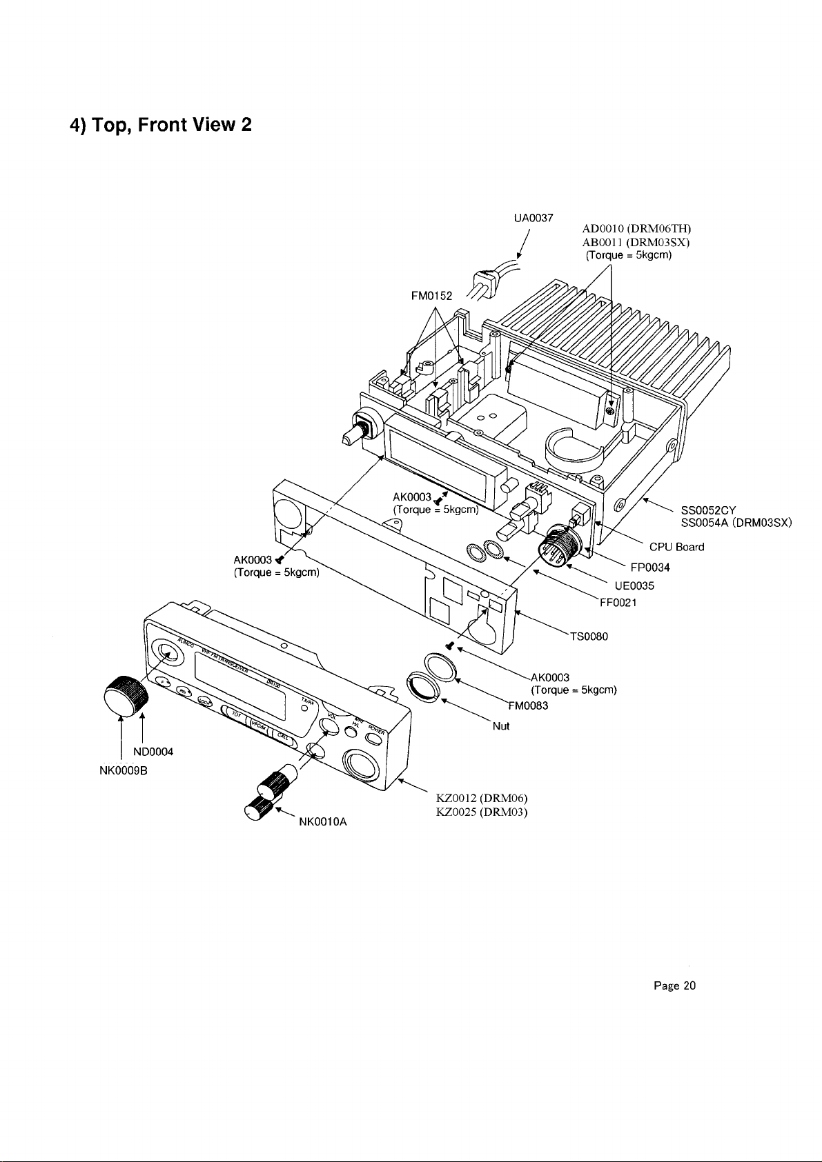
4) Top, Front View 2
FM0152
UA0037
AD0010 (DRM06TH)
AB0011 (DRM03SX)
(Torque = 5kgcm)
Page 21
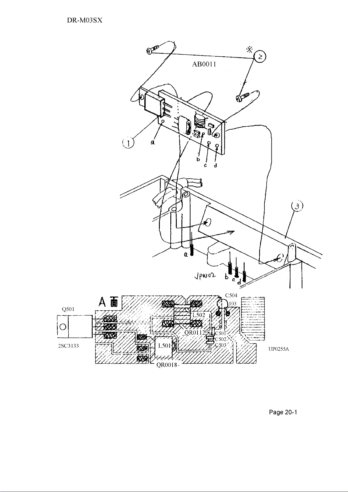
DR-M03SX
Q501
o
2SC3133
QR0018-
C504
__
UP0255A
Page 20-1
Page 22
PARTS LIST
UNIT REF
CPU C201 CU3035 C1608JB1H102KTA 1 1 CPU PL202 EP0003 Lamp(BQ031-30403A) 1 1 1 CPU R271 RK3046 ERJ3GSYJ472V 1 1 1
CPU C202 CU3035 C1608JB1H102KTA 1 1 CPU Q201 XT0095 2SC4081T106R 1 1 1 CPU R272 RK3058 ERJ3GSYJ473V 1 1 1
CPU C203 CU3035 C1608JB1H102KTA 1 1 CPU Q202 XT0113 2SC2873YTE12L 1 1 1 CPU R273 RK3058 ERJ3GSYJ473V 1 1 1
CPU C204 CU3035 C1608JB1H102KTA 1 1 CPU Q203 XU0029 DTC114YUT106 1 1 1 CPU R274 RK3038 ERJ3GSYJ102V 1 1 1
CPU C205 CU3101 C1608JB1C473KTA 1 1 CPU Q204 XU0145 DTC143TUT106 1 1 1 CPU R275 RK3062 ERJ3GSYJ104V 1 1 1
CPU C206 CE0312 ECEV1CA100R 1 1 CPU Q205 XU0112 DTA114YUT106 1 1 1 CPU R276 RK3034 ERJ3GSYJ471V 1 1 1
CPU C207 CU3035 C1608JB1H102KTA 1 1 CPU Q206 XU0112 DTA114YUT106 1 1 1 CPU R277 RK3034 ERJ3GSYJ471V 1 1 1
CPU C208 CS0232 TMCMA1V474MTR 1 1 CPU Q207
CPU C209 CU3035 C1608JB1H102KTA 1 1 CPU Q208 XU0060 UMC2TR 1 1 1 CPU R279 RK3001 ERJ3GSY0R00V 1 1 1
CPU C210 CU3035 C1608JB1H102KTA 1 1 CPU Q209 XU0112 DTA114YUT106 1 1 1 CPU R280 RK3038 ERJ3GSYJ102V 1 1 1
CPU C211 CU3035 C1608JB1H102KTA 1 1 CPU R201 RK3062 ERJ3GSYJ104V 1 1 1 CPU R281 RK3038 ERJ3GSYJ102V 1 1 1
CPU C212 CU3035 C1608JB1H102KTA 1 1 CPU R202 RK3052 ERJ3GSYJ153V 1 1 1 CPU R282
CPU C213 CU3035 C1608JB1H102KTA 1 1 CPU R203 RK3072 ERJ3GSYJ684V 1 1 1 CPU R283
CPU C214
CPU C215 CU3035 C1608JB1H102KTA 1 1 CPU R205 RK3043 ERJ3GSYJ272V 1 1 1 CPU R285
CPU C216 CU3059 C1608JF1E104ZTA 1 1 CPU R206 RK3026 ERJ3GSYJ101V 1 1 1 CPU R286
CPU C217 CU3051 C1608JB1E223KTA 1 1 CPU R207 RK3038 ERJ3GSYJ102V 1 1 1 CPU R287 RK3001 ERJ3GSY0R00V 1 1 1
CPU C218 CU3059 C1608JF1E104ZTA 1 1 CPU R208 RK3026 ERJ3GSYJ101V 1 1 1 CPU R288 RK3052 ERJ3GSYJ153V 1 1 1
CPU C219 CU3059 C1608JF1E104ZTA 1 CPU R209 RK3074 ERJ3GSYJ105V 1 1 1 CPU R289 RK3052 ERJ3GSYJ153V 1 1 1
CPU C220 CU3059 C1608JF1E104ZTA 1 1 CPU R210 RK3052 ERJ3GSYJ153V 1 1 1 CPU R290 RK3052 ERJ3GSYJ153V 1 1 1
CPU C221 CU3023 C1608CH1H101JTA 1 1 CPU R211 RK3062 ERJ3GSYJ104V 1 1 1 CPU R291 RK3052 ERJ3GSYJ153V 1 1 1
CPU C222 CU3023 C1608CH1H101JTA 1 1 CPU R212 RK3054 ERJ3GSYJ223V 1 1 1 CPU R292 RK3052 ERJ3GSYJ153V 1 1 1
CPU C223 CU3051 C1608JB1E223KTA 1 1 CPU R213 RK3070 ERJ3GSYJ474V 1 1 1 CPU R293 RK3050 ERJ3GSYJ103V 1 1 1
CPU C224
CPU C225 CU3023 C1608CH1H101JTA 1 1 CPU R215 RK3102 ERJ3GSYJ203V 1 1 1 CPU R295 RK3001 ERJ3GSY0R00V 1 1 1
CPU C226 CU3023 C1608CH1H101JTA 1 1 CPU R216 RK3050 ERJ3GSYJ103V 1 1 1 CPU R296 RK3038 ERJ3GSYJ102V 1 1 1
CPU C227 CU3035 C1608JB1H102KTA 1 1 CPU R217 RK3102 ERJ3GSYJ203V 1 1 1 CPU R297 RK3038 ERJ3GSYJ102V 1 1 1
CPU C228
CPU C229 CS0209 TMCMB0J106MTR 1 1 CPU R219 RK3102 ERJ3GSYJ203V 1 1 1 CPU R1023 RK3001 ERJ3GSY0R00V 1
CPU C230 CU3035 C1608JB1H102KTA 1 1 CPU R220 RK3050 ERJ3GSYJ103V 1 1 1 CPU S201 UU0015 SKQD-901 1 1 1
CPU C231 CE0312 ECEV1CA100R 1 1 CPU R221 RK3102 ERJ3GSYJ203V 1 1 1 CPU S202 UU0015 SKQD-901 1 1 1
CPU C232
CPU C233
CPU C234 CU3035 C1608JB1H102KTA 1 1 CPU R224 RK3055 ERJ3GSYJ273V 1 1 1 CPU S205 UU0015 SKQD-901 1 1 1
CPU C235 CU3047 C1608JB1H103KTA 1 1 CPU R225 RK3046 ERJ3GSYJ472V 1 1 1 CPU S206 UU0015 SKQD-901 1 1 1
CPU C236 CU3031 C1608JB1H471KTA 1 1 CPU R226 RK3070 ERJ3GSYJ474V 1 1 1 CPU S207 UU0015 SKQD-901 1 1 1
CPU C237 CU3035 C1608JB1H102KTA 1 1 CPU R227 RK3038 ERJ3GSYJ102V 1 1 1 CPU S209 UQ0011 ESB-64801 1 1 1
CPU C238 CU3035 C1608JB1H102KTA 1 1 CPU R228 RK3038 ERJ3GSYJ102V 1 1 1 CPU S210 UR0002 EVQ-WQGF1524B 1 1 1
CPU C239 CU3023 C1608CH1H101JTA 1 1 CPU R229 RK3038 ERJ3GSYJ102V 1 1 1 CPU VR201 RV0009 EVU-F2AF20B14 1 1 1
CPU C240 CU3023 C1608CH1H101JTA 1 1 CPU R230 RK3038 ERJ3GSYJ102V 1 1 1 CPU VR202 RV0009 EVU-F2AF20B14 1 1 1
CPU C241 CU3023 C1608CH1H101JTA 1 1 CPU R231 RK3038 ERJ3GSYJ102V 1 1 1 CPU W1
CPU C242 CU3035 C1608JB1H102KTA 1 1 CPU R232 RK3050 ERJ3GSYJ103V 1 1 1 CPU W2
CPU C243 CS0237 TMCMA1A475MTR 1 1 CPU R233
CPU C244 CU3051 C1608JB1E223KTA 1 1 CPU R234 RK3038 ERJ3GSYJ102V 1 1 1 CPU Y201 TT1002 Tube(1.0X1MM)
CPU C245 CS0237 TMCMA1A475MTR 1 1 CPU R235 RK3038 ERJ3GSYJ102V 1 1 1 CPU Y203 TT1002 Tube(1.0X1MM)
CPU C246 CU3035 C1608JB1H102KTA 1 1 CPU R236 RK3074 ERJ3GSYJ105V 1 1 1 CPU Y202 YZ0042 Cement(G17 1g) 1 1 1
CPU C247 CU3085 C1608CH1H300JTA 1 1 CPU R237
CPU C248 CU3085 C1608CH1H300JTA 1 1 CPU R238 RK3038 ERJ3GSYJ102V 1 1 1 MAIN C2 CU3044 C1608JB1H562KTA 1 1 1
CPU C249 CS0218 TMCMD1A476MTR 1 1 CPU R239
CPU C250 CU3043 C1608JB1H472KTA 1 1 CPU R240
CPU C251 CU3043 C1608JB1H472KTA 1 1 CPU R241 RK3062 ERJ3GSYJ104V 1 1 1 M AIN C5 CU3002 C1608CH1H010CTA 1 1 1
CPU C252 CU3059 C1608JF1E104ZTA 1 1 CPU R242 RK3062 ERJ3GSYJ104V 1 1 1 M AIN C6 CU3002 C1608CH1H010CTA 1 1 1
CPU CN201UE0170 B9B-ZR 1 1 CPU R243 RK3062 ERJ3GSYJ104V 1 1 1 M AIN C7 CU3035 C1608JB1H102KTA 1 1 1
CPU CN202UE0192 11R-JE 1 1 CPU R244 RK3062 ERJ3GSYJ104V 1 1 1 M A IN C8 CS0049 TMCSA1C105MTR 1 1 1
CPU CN203UE0192 11R-JE 1 1 CPU R245
CPU CN204
CPU D201 XD0255 MA8110H-TX 1 1 CPU R247 RK3050 ERJ3GSYJ103V 1 1 1 M AIN C11 CU3047 C1608JB1H103KTA 1 1 1
CPU D202 XD0127 MA704WA-TX 1 1 CPU R248 RK3050 ERJ3GSYJ103V 1 1 1 MAIN C12 CU3047 C1608JB1H103KTA 1 1 1
CPU D203 XD0230 DAN202UT106 1 1 CPU R249 RK3050 ERJ3GSYJ103V 1 1 1 MAIN C13 CU3047 C1608JB1H103KTA 1 1 1
CPU D204 XD0230 DAN202UT106 1 1 CPU R250 RK3046 ERJ3GSYJ472V 1 1 1 MAIN C14 CU3047 C1608JB1H103KTA 1 1 1
CPU D205 XL0029 TLSG264 1 1 CPU R251 RK3046 ERJ3GSYJ472V 1 1 1 M AIN C15 CU3047 C1608JB1H103KTA 1 1 1
CPU DS201 EL0024 LCD(HLC8290 013300) 1 1 CPU R252 RK3046 ERJ3GSYJ472V 1 1 1 M A IN C16 CU3102 C1608JB1C333KTA 1 1 1
CPU IC201 XA0272A CPU(M37410M6H276F! 1 1 CPU R253 RK3038 ERJ3GSYJ102V 1 1 1 MAIN C17 CU3059 C1608JF1E104ZTA 1 1 1
CPU IC202 XA0364 IC(AT24C02N-10SI-2.7) 1 1 CPU R254 RK3038 ERJ3GSYJ102V 1 1 1 M AIN C18 CU8042 C2012JB1C104KTA 1 1 1
CPU IC203
CPU IC204
CPU IC205 XA0238 IC(AN78L05M-E1) 1 1 CPU R257 RK3001 ERJ3GSY0R00V 1 1 1 MAIN C21 CU3028 C1608CH1H271KTA 1 1 1
CPU IC206 XA0208 IC(RH5VL45AA) 1 1 CPU R258 RK3046 ERJ3GSYJ472V 1 1 1 M AIN C22 CU3035 C1608JB1H102KTA 1 1
CPU IC207 XA0198 IC(RH5VL32AA-TI) 1 1 CPU R259 RK3054 ERJ3GSYJ223V 1 1 1 M AIN C22 CU3047 C1608JB1H103KTA 1
CPU IC208 XA0226 IC(X24C08S14-3.0) 1 1 CPU R260 RK3038 ERJ3GSYJ102V 1 1 1 M A IN C23 CU3047 C1608JB1H103KTA 1 1 1
CPU IC209 XA0236 IC(BU4052BCF-E2) 1 1 CPU R261 RK3038 ERJ3GSYJ102V 1 1 1 M AIN C24 CU3059 C1608JF1E104ZTA 1 1 1
CPU JK201 UE0035 mic Jack(FM214-8SMPY 1 1 CPU R262 RK3038 ERJ3GSYJ102V 1 1 1 M AIN C25 CU3102 C1608JB1C333KTA 1 1 1
CPU M201 FM0077Z LCD Holder(DR130) 1 1 CPU R263 RK3038 ERJ3GSYJ102V 1 1 1 M A IN C26 CU3047 C1608JB1H103KTA 1 1 1
CPU M202 FG0133 Conductor(for DR130) 1 1 CPU R264 RK3038 ERJ3GSYJ102V 1 1 1 M AIN C27 CU3049 C1608JB1E153KTA 1 1 1
CPU M203 TL0008 LCD Filter(DR130T) 1 1 CPU R265 RK3050 ERJ3GSYJ103V 1 1 1 M AIN C28 CE0340 16MV 47HW+TS 1 1
CPU M204 FP0034 Mic Spacer(DR110) 1 1 CPU R266 RK3038 ERJ3GSYJ102V 1 1 1 MAIN C29 CE0343 16MV 1000HC+T 1 1 1
CPU M205 FP0069 Xtal Sheet(DJP7) 1 1 CPU R267 RK3038 ERJ3GSYJ102V 1 1 1 MAIN C30 CE0342 16MV 470HC+TS 1 1 1
CPU M206 DG0013Y LCD Light(for DR130) 1 1 CPU R268 RK3038 ERJ3GSYJ102V 1 1 1 M A IN C31 CS0049 TMCSA1C105MTR 1 1 1
CPU PL201 EP0003 Lamp(BQ031-30403A) 1 1 CPU R269 RK3054 ERJ3GSYJ223V 1 1 1 MAIN C32 CE0340 16MV 47HC+TS 1 1 1
PART
SCODE DESCRIPTION 06T06TH03SX UNIT REF
- -
- -
- -
- -
- -
- -
-
-
0 CPU R204 RK3052 ERJ3GSYJ153V 1 1 1 CPU R284
0 CPU R214 RK3058 ERJ3GSYJ473V 1 1 1 CPU R294
0 CPU R218 RK3050 ERJ3GSYJ103V 1 1 1 CPU R298 RK3038 ERJ3GSYJ102V 1 1 1
0 CPU R222 RK3102 ERJ3GSYJ203V 1 1 1 CPU S203 UU0015 SKQD-901 1 1 1
0 CPU R223 RK3058 ERJ3GSYJ473V 1 1 1 CPU S204 UU0015 SKQD-901 1 1 1
0 CPU R246
0 CPU R255 RK0014 ERJ6GEYJ680V 1 1 1 MAIN C19
0 CPU R256 RK3042 ERJ3GSYJ222V 1 1 1 M A IN C20 CU3035 C1608JB1H102KTA 1 1 1
CPU R270 RK3044 ERJ3GSYJ332V 1 1 1 M AIN C33 CE0337 50MV 2R2SW+TS 1 1 1
PARTS
CODE DESCRIPTION 06T06TH03SX UNIT REF
- -
- -
- -
- -
- -
- -
- -
0 CPU R278
0 CPU X203 XQ0045 DSMAT3.58MHZ 18P 1 1 1
0 MAIN C1 CU3035 C1608JB1H102KTA 1 1 1
0 M AIN C3 CU3100 C1608JB1C393KTA 1 1 1
0 MAIN C4 CU3044 C1608JB1H562KTA 1 1 1
0 MAIN C9 CU3059 C1608JF1E104ZTA 1 1 1
0 M AIN C10 CU3059 C1608JF1E104ZTA 1 1 1
PARTSC
ODE DESCRIPTION 06T06TH03SX
- -
- -
- -
- -
- -
- -
- -
- -
- -
- -
0 0 0
0 0 0
0 0 0
0 0 0
0 0 0
Page 22
Page 23

PARTS LIST
UNIT REF
MAIN C34 CE0340 16MV 47HC+TS 1 1 1 M AIN C101 CU3047 C1608JB1H103KTA 1 1 1 M AIN D15 XD0254 1SS355 TE17 1 1 0
MAIN C35 CU3035 C1608JB1H102KTA 1 1 1 M AIN C102
MAIN C36 CU3047 C1608JB1H103KTA 1 1 1 MAIN C103 CU3019 C1608CH1H470JTA 1 1 0 MAIN D17 XD0250 MA742-TX 1 1 1
MAIN C37
MAIN C38 CE0339 1 1 1 MAIN C104 CU3035 C1608JB1H102KTA 1 1 0 MAIN D19 XD0130 DA204UT106 1 1 1
MAIN C39 CU3031 C1608JB1H471KTA 1 1 1 MAIN C104 1 M AIN D20 XD0145 DTZ2.2ATT11 1 1 1
MAIN C40 CS0049 TMCSA1C105MTR 1 1 1 M AIN C105 CE0340 16MV 47HC+TS 1 1 1 M AIN FL1 XC0001 CFW455F 1 1
MAIN C41 CU3047 C1608JB1H103KTA 1 1 1 MAIN C106 CU3019 C1608CH1H470JTA 1 1 0 M AIN FL1 XC0017 CFW455G 1
MAIN C42 CU3035 C1608JB1H102KTA 1 1 1 MAIN C106 CU3023 C1608CH1H101JTA 1 MAIN FL2 XF0004 XF 49U-10.7M15B 1 1 1
MAIN C43 CU3017 C1608CH1H330JTA 1 1 0 MAIN C107 CU3035 C1608JB1H102KTA 1 1 1 M A IN IC1 XA0068 M5218FP-T01-1 1 1 1
MAIN C43 CU3031 C1608JB1H471KTA 0 0 1 MAIN C108 CU3035 C1608JB1H102KTA 1 1 1 MAIN IC2 XA0082 MC7808CT 1 1 1
MAIN C44
MAIN C45
MAIN C46 CU3059 C1608JF1E104ZTA 1 1 1 M AIN C111 CU3035 C1608JB1H102KTA 1 1 1 MAIN IC5 XA0271 M57735 1 1 1
MAIN C47
MAIN C48 CU3035 C1608JB1H102KTA 1 1 1 MAIN C112 CU9029 CM316CH151J100AT 1 M AIN JK1 UA0039 Power Cable( PLUG 4A) 1 1
MAIN C49 CU3024 C1608CH1H121KTA 1 1 1 MAIN C113 CU3035 C1608JB1H102KTA 1 1 1 M AIN JK1 UA0037Y Power Cable(PLUG15A) 1
MAIN C50 CU3017 C1608CH1H330JTA 1 1 1 M A IN C114 CU3035 C1608JB1H102KTA 1 1 1 MAIN JK2 UE0257 ANT.Cable with Connec 1 1 1
MAIN C51 CE0339 16MV 10SW+TS 1 1 1 MAIN C115 CU3023 C1608CH1H101JTA 1 1 1 MAIN JK4 UJ0024 HSJ1403-01-010 1 1 1
MAIN C52 CE0339 16MV 10SW+TS 1 1 1 M AIN C116 CU3035 C1608JB1H102KTA 1 1 1 M A IN L1 QC0126 NL322522T-R22J3 1 1 0
MAIN C53 CS0049 TMCSA1C105MTR 1 1 1 M AIN C117 CU3035 C1608JB1H102KTA 1 1 1 MAIN L2 QC0126 NL322522T-R22J3 1 1 0
MAIN C54 CS0237 TMCMA1A475MTR 1 1 1 MAIN C118 CE0339 16MV 10SW+TS 1 1 1 M AIN L3 QC0048 NL322522T-100J 1 1 1
MAIN C55 CU3035 C1608JB1H102KTA 1 1 1 M AIN C119 CE0338 25MV 4R7SW+TS 1 1 1 M A IN L4 QA0101 QA0101 1 1 0
MAIN C56 CU3003 C1608CH1H020CTA 1 1 1 MAIN C120 CU3035 C1608JB1H102KTA 1 1 1 MAIN L5 QA0101 QA0101 1 1 0
MAIN C57 CU3031 C1608JB1H471KTA 1 1 1 MAIN C121 CU3035 C1608JB1H102KTA 1 1 1 MAIN L6 QA0101 QA0101 1 1 0
MAIN C58 CU3031 C1608JB1H471KTA 1 1 1 MAIN C122 CE0341 16MV 100HC+TS 1 1 1 M AIN L7 QC0126 NL322522T-R22J3 1 1 0
MAIN C59 CU3015 C1608CH1H220JTA 1 1 1 M A IN C123 CU4033 GRM42-6X7R102KJ500P 1 1 1 M A IN L8 QC0126 NL322522T-R22J3 1 1 0
MAIN C60 CE0339 16MV 10SW+TS 1 1 1 MAIN C124 CU3023 C1608CH1H101JTA 1 1 0 MAIN L9 QKA75G COIL MR5.0 7.5T 0.6 1 1 0
MAIN C61 CU3022 C1608CH1H820JTA 1 1 1 MAIN C124 CU3031 C1608JB1H471KTA 1 M AIN L10 QKA75G COIL MR5.0 7.5T 0.6 1 1 0
MAIN C62 CU3023 C1608CH1H101JTA 1 1 0 MAIN C125 CU3035 C1608JB1H102KTA 1 1 1 MAIN L11 QKA55G COIL MR5.0 5.5T 0.6 1 1 0
MAIN C62 CU3047 C1608JB1H103KTA 1 M AIN C126 CU3002 C1608CH1H010CTA 1 1 0 M AIN L12 QKA75G COIL MR5.0 7.5T 0.6 1 1 0
MAIN C63 CE0339 16MV 10SW+TS 1 1 1 MAIN C126 CU3099 C1608CH1H2R5CTA 1 M AIN L13 QC0338 SP0406-3R3-6 1 1 1
MAIN C64 CU3005 C1608CH1H040CTA 1 1 1 MAIN C127 CU3035 C1608JB1H102KTA 1 1 1 M AIN L14 QA0101 QA0101 1 1 0
MAIN C65 CU4022 GRM42-6CH820J500PT 1 0 MAIN C128 CU3035 C1608JB1H102KTA 1 1 1 M AIN L15 QC0126 NL322522T-R22J3 1 1 0
MAIN C65 CU4023 GRM42-6CH101J500PT 1 0 MAIN C129 CU3035 C1608JB1H102KTA 1 1 1 M AIN L16 QKA55G COIL MR5.0 5.5T 0.6 1 1 0
MAIN C65 CU9030 CM316CH181J100AT 1 MAIN C130 CU3039 C1608JB1H222KTA 1 1 1 M AIN L17 QC0048 NL322522T-100K 1 1 1
MAIN C66 CU4022 GRM42-6CH820J500PT 1 1 0 MAIN C131 CU3035 C1608JB1H102KTA 1 1 1 M AIN L1 QC0082 Coil(3225 47 UH) 0 0 1
MAIN C66 CU9029 CM316CH151J100AT 1 MAIN C132 CE0339 16MV 10SW+TS 1 1 1 M A IN L2 QC0039 Coil(3225 1.0 UH) 0 0 1
MAIN C67 CU4022 GRM42-6CH820J500PT 1 0 MAIN C133 CU3035 C1608JB1H102KTA 1 1 1 M AIN L4 QA0117 Coil(BOBBIN QA0117) 0 0 1
MAIN C67 CU4018 GRM42-6CH390J500PT 1 0 M AIN C134 CU3023 C1608CH1H101JTA 1 1 1 M AIN L5 QA0117 Coil(BOBBIN QA0117) 0 0 1
MAIN C67 CU9031 CM316CH221J100AT 1 M A IN C135 CU3023 C1608CH1H101JTA 1 1 1 M A IN L6 QA0117 Coil(BOBBIN QA0117) 0 0 1
MAIN C68 CU3019 C1608CH1H470JTA 1 1 0 MAIN C136
MAIN C68 CU3023 C1608CH1H101JTA 1 M AIN C137
MAIN C69 CU3035 C1608JB1H102KTA 1 1 0 M AIN C138
MAIN C69 CU3047 C1608JB1H103KTA 1 M AIN C139 CU4019 GRM42-6CH470J500PT 1 1 1 M AIN L10 QKA95G Coil(MR5.0 9.5T 0.6) 0 0 1
MAIN C70 CU3019 C1608CH1H470JTA 1 1 0 MAIN C140 CS0232 TMCMA1V474MTR 1 1 1 MAIN L11 QKA75G Coil(MR5.0 7.5T 0.6) 0 0 1
MAIN C70 CU3023 C1608CH1H101JTA 1 MAIN C141 CU3035 C1608JB1H102KTA 1 1 1 MAIN L12 QKA95G Coil(MR5.0 9.5T 0.6) 0 0 1
MAIN C71 CU3035 C1608JB1H102KTA 1 1 1 M AIN C142 CU3035 C1608JB1H102KTA 1 1 1 MAIN L14 QA0117 Coil(BOBBIN QA0117) 0 0 1
MAIN C72 CS0049 TMCSA1C105MTR 1 1 1 M AIN C143 CU3027 C1608CH1H221KTA 1 1 1 M AIN L15 QC0129 Coil(3225 .39 UH) 0 0 1
MAIN C73 CU3035 C1608JB1H102KTA 1 1 1 M AIN C144 CU3023 C1608CH1H101JTA 1 1 1 MAIN L16 QKA75G Coil(MR5.0 7.5T 0.6) 0 0 1
MAIN C74 CU3035 C1608JB1H102KTA 1 1 1 MAIN C145 CU3014 C1608CH1H180JTA 1 1 1 MAIN Q1 XE0012 3SK131V11.12T1 1 1 1
MAIN C75 CU3035 C1608JB1H102KTA 1 1 1 MAIN C146 CU3047 C1608JB1H103KTA 1 1 1 M AIN Q2 XE0012 3SK131V11.12T1 1 1 1
MAIN C76 CU3035 C1608JB1H102KTA 1 1 1 MAIN C147 CU3003 C1608CH1H020CTA 1 1 1 MAIN Q3 XT0094 2SA1576T106R 1 1 1
MAIN C77 CU3019 C1608CH1H470JTA 1 1 0 MAIN C148
MAIN C77 CU3023 C1608CH1H101JTA 1 M A IN C149
MAIN C78 CU3035 C1608JB1H102KTA 1 1 1 MAIN C150 CU4007 GRM42-6CH060J500PT 1 1 0 MAIN Q6 XT0095 2SC4081T106R 1 1 1
MAIN C79 CU3047 C1608JB1H103KTA 1 1 1 MAIN C150 CU4013 GRM42-6CH150J500PT 0 0 1 MAIN Q7 XT0061 2SB1132T100Q 1 1 1
MAIN C80 CU3014 C1608CH1H180JTA 1 1 1 M AIN C151
MAIN C81 CU3047 C1608JB1H103KTA 1 1 1 MAIN C152
MAIN C82 CU3035 C1608JB1H102KTA 1 1 1 MAIN C153 CU3023 C1608CH1H101JTA 1 1 1 MAIN Q10 XU0131 DTC114EUT106 1 1 1
MAIN C83 CU3035 C1608JB1H102KTA 1 1 1 MAIN C154 CU3035 C1608JB1H102KTA 0 0 1 M AIN
MAIN C84 CU3035 C1608JB1H102KTA 1 1 1 MAIN CN1 UE0191 11PS-JE 1 1 1 M AIN Q12 XU0112 DTA114YUT106 1 1 1
MAIN C85 CU3035 C1608JB1H102KTA 1 1 1 M AIN CN2 UE0191 11PS-JE 1 1 1 M AIN Q13 XT0112 2SB1292F 1 1 1
MAIN C86 CU3035 C1608JB1H102KTA 1 1 1 MAIN CN3 UE0043 PI22A02M 1 1 1 MAIN Q14 XT0095 2SC4081T106R 1 1 1
MAIN C87 CU3035 C1608JB1H102KTA 1 1 1 M AIN D1 XD0136 DTZ5.1ATT11 1 1 1 MAIN Q15 XT0084 2SC2954T1 1 1 1
MAIN C88 CU3002 C1608CH1H010CTA 1 1 0 M A IN D2 XD0014 MI308 1 1 0 M A IN Q16 XT0095 2SC4081T106R 1 1 1
MAIN C88 CU3099 C1608CH1H2R5CTA 1 MAIN D2 XD0285 1SS53 0 1 MAIN Q17 XU0152 UMC5TR 1 1 1
MAIN C89 CU3035 C1608JB1H102KTA 1 1 1 MAIN D3 XD0014 MI308 1 1 0 MAIN Q18 XE0021 2SK880GRTE85L 1 1 1
MAIN C90 CU3035 C1608JB1H102KTA 1 1 1 MAIN D3 XD0287 1N4002 0 1 M A IN Q19 XT0096 2SC4099T106N 1 1 1
MAIN C91 CU3035 C1608JB1H102KTA 1 1 1 M AIN D4 XD0254 1SS355 TE17 0 1 1 MAIN Q20 XT0059 2SC3082KT146Q 1 1
MAIN C92 CU3019 C1608CH1H470JTA 1 1 1 M A IN D5 XD0130 DA204UT106 1 1 1 MAIN Q20 XT0030 Transistor(2SC3356T1) 1
MAIN C93 CU3035 C1608JB1H102KTA 1 1 1 MAIN D6 XD0254 1SS355 TE17 1 1 1 M AIN Q21 XT0099 2SA1736YTE12L 1 1 1
MAIN C94 CS0049 TMCSA1C105MTR 1 1 1 M AIN D7
MAIN C95 CU3035 C1608JB1H102KTA 1 1 1 M AIN D8 XD0254 1SS355 TE17 1 1 1 MAIN Q23 XT0084 2SC2954T1 1
MAIN C96 CU3035 C1608JB1H102KTA 1 1 1 MAIN D9 XD0107 G3B 1 1 1 MAIN Q24 XU0131 DTC114EUT106 1 1 1
MAIN C97 CU3023 C1608CH1H101JTA 1 1 1 MAIN D10 XD0254 1SS355 TE17 1 1 1 M AIN Q28 XT0095 2SC4081T106R 1 1 1
MAIN C98 CU0071 C2012CH1H101JTA 1 1 1 MAIN D11 XD0260 1SV231TPH4 1 1 1 MAIN Q29
MAIN C99 CU3019 C1608CH1H470JTA 1 1 0 MAIN D12 XD0260 1SV231TPH4 1 1 1 MAIN Q30 XU0125 DTA144EUT106 1 1 1
MAIN C99 CU3027 C1608CH1H221JTA 0 0 1 M AIN D13 XD0260 1SV231TPH4 1 1 1 M AIN R1 RK0105 ERJ6GEYJ2R2V 1 1 1
MAIN C100 CU3035 C1608JB1H102KTA 1 1 1 MAIN D14 XD0246 DAN235UT106 1 1 1 MAIN R2 RK4034 ERJ-12YJ471V 1 1 1
PART
SCODE DESCRIPTION 06T06TH03SX UNIT REF
- -
- -
- -
- -
0 M AIN C103 CU3023 C1608CH1H101JTA 1 M AIN D18 XD0250 MA742-TX 1 1 1
0 0 0 MAIN C109 CU3003 C1608CH1H020CTA 1 1 1 MAIN IC3 XA0144 TK10487M 1 1 1
0 0 0 MAIN C110 CU3003 C1608CH1H020CTA 1 1 1 MAIN IC4 XA0079 UPC1241H 1 1 1
0 0 0 MAIN C112 CU4019 GRM42-6CH470J500PT 1 1 MAIN IC6 XA0119 AN8010M-E1 1 1 1
PARTS
CODE DESCRIPTION 06T06TH03SX UNIT REF
- -
- -
- -
- -
- -
- -
- -
- -
- -
0 M AIN D16 XD0260 1SV231TPH4 1 1 1
0 0 0 MAIN L7 QC0129 Coil(3225 .39 UH) 0 0 1
0 0 0 MAIN L8 QC0129 Coil(3225 .39 UH) 0 0 1
0 0 0 MAIN L9 QKA85G Coil(MR5.0 8.5T 0.6) 0 0 1
0 0 0 MAIN Q4 XT0095 2SC4081T106R 1 1 1
0 0 0 MAIN Q5 XT0095 2SC4081T106R 1 1 1
0 0 0 MAIN Q8 XT0096 2SC4099T106N 1 1 1
0 0 0 MAIN Q9 XT0037 2SC2412KT146R 1 1 1
Q11
0 0 MAIN Q22 XT0095 2SC4081T106R 1 1 1
PARTSC
ODE DESCRIPTION 06T06TH03SX
XU0148 DTC144EUT106 1 1 1
- -
Page 23
Page 24

PARTS LIST
UNIT REF
MAIN R3 RK3050 ERJ3GSYJ103V 1 1 1 M AIN R82 RK3038 ERJ3GSYJ102V 1 1 1 VCO C313 CU3035 C1608JB1H102KTA 1 1 1
MAIN R4 RK3071 ERJ3GSYJ564V 1 1 1 M AIN R83 RK3022 ERJ3GSYJ470V 1 1 1 VCO C314 CU3043 C1608JB1H472KTA 1 1 1
MAIN R5 RK3034 ERJ3GSYJ471V 1 1 1 MAIN R84 RK3034 ERJ3GSYJ471V 1 1 1 VCO C315
MAIN R6 RK3062 ERJ3GSYJ104V 1 1 1 M AIN R85 RK3043 ERJ3GSYJ272V 1 1 1 VCO C316 CU3035 C1608JB1H102KTA 1 1 1
MAIN R7 RK3042 ERJ3GSYJ222V 1 1 1 M A IN R86 RK3045 ERJ3GSYJ392V 1 1 1 VCO C317 CS0217 TMCMC1A226MTR 1 1 1
MAIN R8 RK3042 ERJ3GSYJ222V 1 1 1 MAIN R87
MAIN R9
MAIN R10 RK3071 ERJ3GSYJ564V 1 1 1 M AIN R88 RK3018 ERJ3GSYJ220V 1 VCO C320 CU3019 C1608CH1H470JTA 1 1 1
MAIN R11 RK3046 ERJ3GSYJ472V 1 1 1 MAIN R89 RK0028 ERJ6GEYJ471V 1 1 1 VCO C321 CU3031 C1608JB1H471KTA 1 1 1
MAIN R12 RK3038 ERJ3GSYJ102V 1 1 1 M AIN R90
MAIN R13 RK3038 ERJ3GSYJ102V 1 1 1 M AIN R91 RK3001 ERJ3GSY0R00V 1 1 1 VCO C323 CU3006 C1608CH1H050CTA 1 1
MAIN R14 RK3071 ERJ3GSYJ564V 1 1 1 M AIN R92 RK3038 ERJ3GSYJ102V 1 1 1 VCO C323 CU3005 C1608CH1H040CTA 1
MAIN R15 RK3050 ERJ3GSYJ103V 1 1 1 M AIN R93 RK3062 ERJ3GSYJ104V 1 1 1 VCO C324 CU3035 C1608JB1H102KTA 1 1 1
MAIN R16 RK4028 ERJ-12YJ151V 1 1 1 MAIN R94 RK3050 ERJ3GSYJ103V 1 1 1 VCO C325 CU3035 C1608JB1H102KTA 1 1 1
MAIN R17 RK3057 ERJ3GSYJ393V 1 1 1 M AIN R95
MAIN R18 RK3042 ERJ3GSYJ222V 1 1 1 M AIN R96 RK3071 ERJ3GSYJ564V 1 1 1 VCO C327 CU3047 C1608JB1H103KTA 1 1 1
MAIN R19 RK3060 ERJ3GSYJ683V 1 1 1 M AIN R97
MAIN R20 RK3060 ERJ3GSYJ683V 1 1 1 M AIN R98 RK0069 ERJ6GEYJ104V 1 1 1 VCO C329 CU3035 C1608JB1H102KTA 1 1 1
MAIN R21 RK3051 ERJ3GSYJ123V 1 1 1 MAIN R99 RK3052 ERJ3GSYJ153V 1 1 1 VCO C330 CU3035 C1608JB1H102KTA 1 1 1
MAIN R22 RK3050 ERJ3GSYJ103V 1 1 1 M AIN R100 RK3044 ERJ3GSYJ332V 1 1 1 VCO C331
MAIN R23 RK3050 ERJ3GSYJ103V 1 1 1 M AIN R101 RK0039 ERJ6GEYJ222V 1 1 VCO C332 CU3035 C1608JB1H102KTA 1 1 1
MAIN R24 RK3050 ERJ3GSYJ103V 1 1 1 M AIN R102 RK3038 ERJ3GSYJ102V 1 1 1 VCO C333 CU3013 1
MAIN R25 RK3047 ERJ3GSYJ562V 1 1 1 M AIN R103 RK3026 ERJ3GSYJ101V 1 1 1 VCO CN301 UE0188 B9P-BC-2 1 1 1
MAIN R26 RK3026 ERJ3GSYJ101V 1 1 1 M AIN R104 RK3050 ERJ3GSYJ103V 1 1 1 VCO CN302 UE0185 B6P-BC-2 1 1 1
MAIN R27 RK3038 ERJ3GSYJ102V 1 1 1 M AIN R105 RK3042 ERJ3GSYJ222V 1 1 1 VCO D301
MAIN R28 RK3058 ERJ3GSYJ473V 1 1 1 MAIN R106 RK3062 ERJ3GSYJ104V 1 1 0 VCO D302 XD0260 1SV231TPH4 1 1
MAIN R29 RK3042 ERJ3GSYJ222V 1 1 1 M AIN R107 RK0001 ERJ6GEYJ100V 1 1 1 VCO D303 XD0130 DA204UT106 1 1 1
MAIN R30 RK3045 ERJ3GSYJ392V 1 1 1 M AIN R108 RK3043 ERJ3GSYJ272V 1 1 1 VCO D304 XD0284 KV1488 1
MAIN R31 RK3054 ERJ3GSYJ223V 1 1 1 MAIN R109 RK3062 ERJ3GSYJ104V 1 1 1 VCO IC301 XA0145 MB1504LPFGBNDTF 1 1 1
MAIN R32 RK3057 ERJ3GSYJ393V 1 1 1 M AIN R110 RK3044 ERJ3GSYJ332V 1 1 1 VCO L302 QA0102 QA0102 1 1 1
MAIN R33 RK3047 ERJ3GSYJ562V 1 1 1 M AIN R111 RK3001 ERJ3GSY0R00V 1 1 1 VCO L303 QC0047 NL322522T-4R7J 1 1 1
MAIN R34 RK4018 ERJ-12YJ220V 1 1 1 MAIN R112 RK3049 ERJ3GSYJ822V 1 1 1 VCO L304
MAIN R35 RK3050 ERJ3GSYJ103V 1 1 1 MAIN R113 RK3050 ERJ3GSYJ103V 1 1 1 VCO L305
MAIN R36 RK3038 ERJ3GSYJ102V 1 1 1 M AIN R114 RK3062 ERJ3GSYJ104V 1 1 1 VCO M301 TS0081 Shield(VCO CASE) 1 1 1
MAIN R37 RK3045 ERJ3GSYJ392V 1 1 1 MAIN R115 RK3038 ERJ3GSYJ102V 1 1 1 VCO YZ0107 Others(VA-30 1cc) 0.1 0.1
MAIN R38 RK3054 ERJ3GSYJ223V 1 1 1 MAIN R116
MAIN R39 RK3032 ERJ3GSYJ331V 1 1 1 M AIN R117 RK3026 ERJ3GSYJ101V 1 1 1 VCO Q302 XT0111 2SC4081LNT106S 1 1 1
MAIN R40 RK3054 ERJ3GSYJ223V 1 1 1 M AIN R118 RK3054 ERJ3GSYJ223V 1 1 1 VCO Q303 XT0111 2SC4081LNT106S 1 1 1
MAIN R41 RK3042 ERJ3GSYJ222V 1 1 1 MAIN R119 RK3038 ERJ3GSYJ102V 1 1 1 VCO Q304 XT0096 2SC4099T106N 1 1 1
MAIN R42 RK3041 ERJ3GSYJ182V 1 1 1 MAIN R120 RK3050 ERJ3GSYJ103V 1 1 1 VCO Q305 XT0096 2SC4099T106N 1 1 1
MAIN R43 RK3058 ERJ3GSYJ473V 1 1 1 MAIN R121 RK3001 ERJ3GSY0R00V 1 1 1 VCO Q306 XT0094 2SA1576T106R 1 1 1
MAIN R44 RK3014 ERJ3GSYJ100V 1 1 1 M AIN R123 RK3046 ERJ3GSYJ472V 1 1 1 VCO Q307
MAIN R45 RK3026 ERJ3GSYJ101V 1 1 1 M AIN R125 RK0107 ERJ6GEY0R00V 1 VCO Q308
MAIN R46
MAIN R47 RK3062 ERJ3GSYJ104V 1 1 1 MAIN TC1 CT0012 CTZ-10AW 1 1 1 VCO R302 RK3050 ERJ3GSYJ103V 1 1 1
MAIN R48 RK3026 ERJ3GSYJ101V 1 1 1 MAIN TH1 XS0040 Thermistor(ERTD2ZGL2 1 1 1 VCO R303 RK3050 ERJ3GSYJ103V 1 1 1
MAIN R49 RK3038 ERJ3GSYJ102V 1 1 1 M AIN TH2 XS0013Z Thermistor(NTH5D682K 1 1 VCO R304
MAIN R50 RK3071 ERJ3GSYJ564V 1 1 1 M AIN VR1 RH0106 EVM1YSX50BQ4 1 1 1 VCO R305
MAIN R51 RK3058 ERJ3GSYJ473V 1 1 1 MAIN VR2 RH0103 EVM1YSX50B14 1 1 1 VCO R306
MAIN R52
MAIN R53 RK3044 ERJ3GSYJ332V 1 1 1 M AIN VR5 RH0106 EVM1YSX50BQ4 1 1 1 VCO R308 RK3046 ERJ3GSYJ472V 1 1 1
MAIN R54 RK4034 ERJ-12YJ471V 1 1 1 MAIN VR6 RH0061 MVR32HXBRN472 1 VCO R309 RK3028 ERJ3GSYJ151V 1 1 1
MAIN R55 RK3050 ERJ3GSYJ103V 1 1 1 M AIN VR6 RH0103 EVM1YSX50B14 1 1 0 VCO R310 RK3045 ERJ3GSYJ392V 1 1 1
MAIN R56 RK3050 ERJ3GSYJ103V 1 1 1 M AIN X1 XQ0063 X 49U-11.15M 1 1 1 VCO R311 RK3044 ERJ3GSYJ332V 1 1 1
MAIN R57 RK3018 ERJ3GSYJ220V 1 1 1 MAIN X2 XK0002 CDBM455C7 1 1 1 VCO R312 RK3047 ERJ3GSYJ562V 1 1 1
MAIN R58 RK3038 ERJ3GSYJ102V 1 1 1 MAIN X3 XQ0064 X 49U-11.155M 1 1 1 VCO R313 RK3039 ERJ3GSYJ122V 1 1 1
MAIN R59 RK3053 ERJ3GSYJ183V 1 1 M AIN Y1 TZ0056 Silicon Dumper(49U) 4 4 4 VCO R314 RK3022 ERJ3GSYJ470V 1 1 1
MAIN R59 RK3054 ERJ3GSYJ223V 1 0 PA C501 CU3021 C1608CH1H680JTA 0 0 1 VCO R315 RK3052 ERJ3GSYJ153V 1 1 1
MAIN R60 RK3034 ERJ3GSYJ471V 1 1 1 PA C502 CU3047 C1608JB1H103KTA 0 0 1 VCO R316 RK3026 ERJ3GSYJ101V 1 1
MAIN R61 RK3038 ERJ3GSYJ102V 1 1 1 PA C503 CU3047 C1608JB1H103KTA 0 0 1 VCO R316 RK3025 ERJ3GSYJ820V 1
MAIN R62 RK3054 ERJ3GSYJ223V 1 1 1 PA Q501 XT0134 Transistor(2SC3133) 0 0 1 VCO R317 RK3026 ERJ3GSYJ101V 1 1 1
MAIN R63 RK3032 ERJ3GSYJ331V 1 1 1 PA L501 QR0018 Coil(DRM03) 0 0 1 VCO R318 RK3051 ERJ3GSYJ123V 1 1 1
MAIN R64 RK3042 ERJ3GSYJ222V 1 1 1 PA L502 QK0112
MAIN R65 RK3026 ERJ3GSYJ101V 1 1 1 PA C504 CK0002 Capacitor(50V 0.01UF) 0 0 1 VCO R320 RK3044 ERJ3GSYJ332V 1 1 1
MAIN R66 RK3050 ERJ3GSYJ103V 1 1 1 PA R126 RD1013 Resistor(1/4 W TYPE 0 ( 0 0 1 VCO R321
MAIN R67 RK3026 ERJ3GSYJ101V 1 1 1 PA R127 RD1013 Resistor(1/4 W TYPE 0 < 0 0 1 VCO R322 RK3034 ERJ3GSYJ471V 1 1 1
MAIN R68 RK3030 ERJ3GSYJ221V 1 1 1 PA R128 RD1013 Resistor(1/4 W TYPE 0 < 0 0 1 VCO R323 RK3054 ERJ3GSYJ223V 1 1 1
MAIN R69 RK3050 ERJ3GSYJ103V 1 1 1 PA R129 RD1013 Resistor(1/4 W TYPE 0 < 0 0 1 VCO R324 RK3034 ERJ3GSYJ471V 1 1 1
MAIN R70 RK3058 ERJ3GSYJ473V 1 1 1 VCO C301
MAIN R71 RK3026 ERJ3GSYJ101V 1 1 1 VCO C302 CS0220 TMCMA1C225MTR 1 1 1 VCO R326 RK3026 ERJ3GSYJ101V 1 1 1
MAIN R72
MAIN R73 RK3052 ERJ3GSYJ153V 1 1 1 VCO C304 CS0063 TMCSA1V104MTR 1 1 1 VCO R328 RK3039 ERJ3GSYJ122V 1 1 1
MAIN R74 RK3052 ERJ3GSYJ153V 1 1 1 VCO C305 CU3035 C1608JB1H102KTA 1 1 1 VCO R329 RK3026 ERJ3GSYJ101V 1 1 1
MAIN R75 RK3052 ERJ3GSYJ153V 1 1 1 VCO C306 CU3047 C1608JB1H103KTA 1 1 1 VCO R330 RK3054 ERJ3GSYJ223V 1 1 1
MAIN R76 RK3026 ERJ3GSYJ101V 1 1 1 VCO C307 CU3035 C1608JB1H102KTA 1 1 1 VCO R331 RK3038 ERJ3GSYJ102V 1 1 1
MAIN R77 RK3050 ERJ3GSYJ103V 1 1 1 VCO C308 CS0235 TMCSA1V334MTR 1 1 1 VCO R332 RK3022 ERJ3GSYJ470V 1 1 1
MAIN R78 RK3026 ERJ3GSYJ101V 1 1 1 VCO C309 CU3043 C1608JB1H472KTA 1 1 1 VCO R333 RK3054 ERJ3GSYJ223V 1 1 1
MAIN R79 RK3038 ERJ3GSYJ102V 1 1 1 VCO C310 CU3043 C1608JB1H472KTA 1 1 1 VCO R334 RK3054 ERJ3GSYJ223V 1 1 1
MAIN R80 RK3050 ERJ3GSYJ103V 1 1 1 VCO C311 CS0237 TMCMA1A475MTR 1 1 1 VCO R335 RK3052 ERJ3GSYJ153V 1 1 1
MAIN R81 RK3052 ERJ3GSYJ153V 1 1 1 VCO C312 CS0237 TMCMA1A475MTR 1 1 1
PART
SCODE DESCRIPTION 06T06TH03SX UNIT REF
- -
- -
- -
- -
0 MAIN R88 RK3014 ERJ3GSYJ100V 1 1 0 VCO C319 CU3035 C1608JB1H102KTA 1 1 1
0 MAIN R130 RK0001 ERJ6GEYJ100V 1 VCO R301 RK3050 ERJ3GSYJ103V 1 1 1
0 M AIN VR4 RH0106 EVM1Y SX50BQ4 1 1 1 VCO R307
0 VCO C303
PARTS
CODE DESCRIPTION 06T06TH03SX UNIT REF
- -
- -
- -
- -
- -
Coil(QK0112)
- -
- -
0 VCO C318 CU3011 C1608CH1H100DTA 1 1 1
0 VCO C322 CU3035 C1608JB1H102KTA 1 1 1
0 VCO C326 CS0235 TMCSA1V334MTR 1 1 1
0 VCO C328
0 VCO Q301 XE0010 2SK508K52-T2B 1 1 1
0 0 1 VCO R319 RK3034 ERJ3GSYJ471V 1 1 1
0 0 0 VCO R325 RK3050 ERJ3GSYJ103V 1 1 1
0 0 0 VCO R327 RK3026 ERJ3GSYJ101V 1 1 1
PARTSC
ODE DESCRIPTION 06T06TH03SX
- -
- -
- -
- -
- -
- -
- -
- -
- -
- -
- -
- -
- -
0 0 0
0 0 0
0 0 0
0 0 0
Page 24
Page 25
PARTS LIST
UNIT REF
Mechanical ES0017 Speaker(057M9017) 1 1 1 SCREW SET AA0013 BH M5+20 FE/ZN 4 4 4 PA C501 CU3021 C1608CH1H180JTA 1
Mechanical FF0015 Cloth(BLIND DR110) 3 3 3 SCREW SET AE0012 HEXH/D M4+8 FE/B.ZÎ 4 4 4 PA C502 CU3047 C1608JB1H103KTA 1
Mechanical FF0021 Cloth(BLIND VOL DR1
Mechanical FF0028 Cloth(10X22) 1 1 1 SCREW SET AN0002 HEX N5X0.8 FE/ZN 4 4 4 PA C504 CK0002 CK45-F1H103ZYA 1
Mechanical FF0029 Cloth(4.0X22) 1 1 1 SCREW SET AZ0009 SW 5X9.2X1.3 FE/ZN 4 4 4 PA R126 RD1013 JPW02 R01 1
Mechanical FF0030 Cloth(5.0X20) SCREW SET AZ0010 SW 5X12X0.8 FE/ZN 4 4 4 PA R127 RD1013 JPW02 R01 1
Mechanical FF0031 Cloth(7.0X30) SCREW SET EF0005 Fuse(FGBO 15A) 2 2 0 PA R128 RD1013 JPW02 R01 1
Mechanical FG0040 Speaker Cushion 1 1 1 SCREW SET FM0079Z Spanner(DR130) 1 1 1 PA R129 RD1013 JPW02 R01 1
Mechanical FG0148 Button Cushion(DR130) 1 1 1 SCREW SET HP0006 Protect.Bag(5X90X170) 1 1 1 PA L501 QR0018 COIL 1
Mechanical FM0152 METAL(IC FIX DR130 PA L502 QK0112 COIL 1
Mechanical FM0083 Washer(DR130) 1 1 1 PA Q501 XT0134 2SC3133 1
Mechanical FP0080 Hidden Board(DR150) 1 1
Mechanical KS0041CZ Bottom Case(DR130) 1 1 1
Mechanical KZ0047AZ Top Case(DR130T) 1 1 1
Mechanical KZ0012 Front Panel(DRM06) 1 1 1
Mechanical ND0004 Cover(DIAL DR110) 1 1 1
Mechanical NK0009B Knob(DIAL DRM06) 1 1 1
Mechanical NK0010A Knob(VOL KN OB)
Mechanical NP0066Z Push Knob(POWER R13 1 1 1
Mechanical NP0067A Key(H/L DR130) 1 1 1
Mechanical SD0034 SPRing(GND DR130) 1 1 1
Mechanical SS0052CY Chassis(DR130) 1
Mechanical SS0054A Chassis(DRM06) 1 1
Mechanical TS0080Z Shield(FRONT DR130) 1 1 1
Mechanical UP0255A P.C.Board(DRM03 INT E 1 1 1
Mechanical UX1047 Wire(DR130) 1 1 1
Mechanical YZ0042 Cement(G17 1PC.) 1 1 1
Mechanical YZ0128 Tape(LCD DR130) 1 1 0
Mechanical AD0010 Screw(PH/D M3+8 FE/
Mechanical AK0003 Screw(0PH B2.6+6 FE/N 3 3 3
Mechanical AE0014 Screw(OH B2.6+8B FE/ 7 7 7
Mechanical AV0001 Screw(BH B2.6+6 FE/N 10 8 10
Mechanical AB0011 Screw(PH/S M3+8 FE/ 0 0 1
Packing ADFM78 BRACKET DR130 1 1 1
Packing
Packing
Packing
Packing
Packing DS0388A Serial No.Plate(NEW) 0 0 1
Packing EMS11 Mic. 1 1 0
Packing EMS5A Mic. 0 0 1
Packing HH0042 STYRO.OUTER DR130 0.4 0.4 0
Packing HH0044A INNER BOX DRM06 0 0 1
Packing HH0046 STYROFOAM DRM06 0 0 1
Packing HK0362A PACKAGE DRM06T 1 1 0
Packing HK0368 PACKAGE DRM03SX 0 0 1
Packing HM0119A 5PCS DR130 0.2 0.2 0
Packing HM0124A PACKAGE DRM10 0 0 0.5
Packing HP0002 5X205X305 0 0 1
Packing HP0026 5X200X400 0 0 1
Packing HP0035 5X200X250 1 1 0
Packing HP0036 5X90X900 1 1 0
Packing HU0047 P.MTL(A)DR130 1 1 0
Packing HU0048 P.MTL(B)DR130 1 1 0
Packing HU0055 P.MTL/C.BD.DRM10 0 0 1
Packing HU0064 P.M TL/CARTON DRM 0 1 0 0
Packing PF0034A CAUTION 0 0 1
Packing PF0048 ADD ITIONAL INST.06 0 1 0
Packing PH0009A WARRA NTY CERT EX 1 0 0
Packing PH0010A Warranty Certificate DO M 0 0 1
Packing PK0071 DIAG RAM DRM06TH 0 1 0
Packing PR0154 Label(H) 0 1 0
Packing PR0237 FCC PART15 1 0 0
Packing PS0201B INSTRUCTION DRM06 1 1 1
Packing PT0004A SERIAL NO.FOR CART 0 0 2
PART
SCODE DESCRIPTION 06T06TH03SX UNIT REF
3 2 2 2 SCREW SET AJ0003 BH T5+20 FE/ZN 1 4 4 4 PA C503 CU3047 C1608JB1H103KTA 1
N 2 2 2
ADUA38 Power Cable(R-B2.0X3m 1 1 1
DK0115 PROTECT.FILM DR130 1 1 1
DS0351 Serial No.Plate(Standardi 0 1 0
DS0354B Serial No.Plate(for DRM 0 1 0 0
PARTS
CODE DESCRIPTION 06T06TH03SX UNIT REF
PARTSC
ODE DESCRIPTION 06T06TH03SX
Page 25
Page 26

ADJUSTMENT
1) Required Test Equipment 11. Distortion Meter
1. Digital Multimeter Measurable frequency:
Voltage range: FS= 18Vorso Input level:
Input resistance: 1M ohm or more Distortion level:
1kHz
Up to 40dB
1% - l00%
2. Regulated Power Supply
Supply voltage: 13.80V
Current : 15A or more
3. Oscilloscope
Measurable frequency: DC to 30MHz
4. Spectrum Analyzer
Measuring range: Up to 2GHz or more
5. Tracking Generator
Output frequency: Up to 2GHz or more
6. Audio Dummy Load
Impedance: 8 ohm
Dissipation: 5W or more
7. SSG
Output frequency:
Output level:
Moduration:
1GHz or more
-20dB/0.1uV to 120dB/1V
FM
12. Audio Generator
Output frequency:
Output impedance:
13. Linear Detector
Measurable frequency:
Characteristics:
CN:
88.5Hz and lkHz
600 ohm, unbalanced
Up to 500MHz
FIat
60dB or more
8. Frequency Counter
Measurable frequency! Up to 500MHz
Measurements stability: 0.2ppm or so
9. Power Meter
Measurable frequency.I Up to 500MHz
Impedance: 50 ohm, unbalanced
Measuring range: Full scale of 60W or so
10. Audio Voltmeter
Measurable frequency: 50Hz to 10kHz
Sensitivity: 1mV ~ 10V
Page 27
Page 27

2) Adjustment for DRM03SX
SS G M o d : 1 K H z + /-3 .5 K H z /D E V
SP te rm in a l is conn e cted to 8 oh m du m m y load.
R X speaker o u tp u t le v e l is 50 to 1 0 0 m W
1. P o w e r s u p p ly v o lta g e is 1 3 .8 V . P o w e r s w itc h is o ff .
2. T u rn th e s q uelch a n d v o lu m e kn o b s co u n te rclo ck w ise .
3. Press a nd h o ld the "F "k e y ,t h e n tu r n o n the p o w e r s w itc h.
Th e d is p lay sho w s th a t th e freq u en c y is 2 9 .0 0 M H z
P L L A d ju s tm e n t
C o n d itio n M ea su re m en t A d ju s tm e n t Specification
Ite m
Freq u en c y Freq ue n cy: 2 9 .0 0 M H z T X
L O W
P L L V C O Freq u en c y: 5 2.0 0M H z T X D ig ita l M a in PD P L L L 3 0 2 8 .2 V 8.1-8 .3 V
Test equipment U n it T e rm in a l U n it Pa rts M e th o d
Fre q .C ou n ter
P o w e r M e te r B a c k A N T M A I N
TC 3 29.00
M H z
+ /- 100 H z
Freq u en c y :1 2 9 .0 3 M H z
SS G ou t: -7 d B u
R X
Sen sitiv ity
S M e te r
S Q L L e ve l
H ig h P o w e r Fre q ue n cy: 2 9 .0 0 M H z T X
L o w P o w e r
M A X D E V
Freq u en c y: 2 9 .0 3 M H z
SS G o u t:-7 d B u
SS G ou t: 0 d B u
Freq u en c y: 4 0 .0 0 M H z
SS G ou t: 3 0d B u
Freq u en c y: 2 9 .0 3 M H z
SS G ou t: 15 d B u
M o d : 1 K H z
Freq u en c y: 2 9 .0 3 M H z
SS G o u t:O F F
M o d : 1 K H z
Freq u en c y: 2 9 .0 3 M H z
SS G o u t:-1 0 d B u
S Q L V R :Th re sh o ld
Freq u en c y: 2 9 .0 0 M H z
P o w e r:L o w *1
Freq u en c y: 2 9 . 0 0 M H z
A G :1 K H z -3 0 d B m
R X
R X
R X
R X
R X C h ec k S M e te r doe s
R X LC D Bu sy
H ig h Po w e r M e te r B a c k A N T M a in
T X
L o w
T X
L o w
Distortion Meter
SSG
M a in M a in
L C D S M e ter F r o n t
Pa n e l
F r o n t
Pa n e l M a in
L 4 -L 6
L 1 4
M a in V R 5
V R 1
V R 6
V R 2 4 .7k H z
S IN A D :
M A X
Turn the coil L14,
L4,L5,L6,L4,L5 to
the MAX in order
S IN A D is
ab o ve 1 2d BFreq u en c y: 2 6 .0 3 M H z
F u ll
flashing
n o t lig h t.
Make
sure
that SQL
B u s y O N
is open
10 .5 W + /- 0 .5 W ( T )
1.0w
+ /- 0 .1 W (T )
4.7 + /-0 .1
/D e v
k H z /D e v
Narrow Version
2.4 + /-0 .2
kH z /D e v
M I C G a in F re qu e ncy : 2 9 .0 0 M H z
A G :1 K H z -4 7 d B m
Freq u en c y : 2 9 .0 0 M H z
C T C S S T o n
D E V
eAG: O F F
T o n e S W ( 8 8 .5H z ):O N
T X
L o w
T X
L o w C he ck 0.60 -0 .8 5
Linear Detector
Power Meter
B a c k A N T M a in
Oscilloscope
V R 4 4 .0 k H z
/D e v
4.0+ /- 0 .1
k H z /D e v
k H z /D e v
2.0 + /-0 .2
kH z /D e v
0.35 - 1 .2
kH z /D e v
Page 28
Page 28

2) Adjustment for DRM06TH/T
SS G M o d : 1 K H z + /-3 .5 K H z /D E V
SP te rm in a l is conn ected to 8o h m du m m y lo a d .
R X speaker o u tp u t le ve l is 50 to 1 0 0 m W
1. P o w e r s u p p ly v o lta g e is 1 3 .8 V . P o w e r s w itc h is o ff .
2. T u rn th e s q ue lch a n d v o lu m e kn o b s co u n te rclo ck w ise .
3. Press a nd h o ld the "F "k e y ,t h e n tu r n o n the p o w e r s w itc h.
Th e d is p lay sho w s th a t th e freq u en c y is 5 1 .00 M H z
P L L A d ju s t m e n t
C o n d itio n M ea su re m en t A d ju s tm e n t Specification
Ite m
Freq u en c y Freq ue n cy: 5 2.0 0M H z T X
L O W
P L L V C O Freq u en c y: 5 2.0 0M H z T X D ig ita l M a in PD P L L L 3 0 2 5 .2 V 5.1-5 .3 V
Test equipment
F re q.C o u n te r
P o w e r M e te r B a c k A N T M A I N
U n it T e rm in a l U n it Pa rts M e th o d
TC 3 5 2 .0 00
M H z
+ /- 100 H z
Freq u en c y :1 5 1 .0 3 M H z
SS G ou t: -1 0 d B u
R X
Sen sitiv ity
S M e te r
S Q L L e ve l
H ig h P o w e r F re q uen c y: 5 2.0 0 M H z T X
L o w P o w e r
M A X D E V
M I C G a in F re qu e ncy : 5 2 .00 M H z
C T C S S T o n
D E V
Freq u en c y: 5 1.0 3 M H z
SS G o ut:-1 0 d B u
Freq u en c y: 5 9.0 3 M H z
SS G out: 0 d B u
Freq u en c y: 5 1.0 3 M H z
SS G ou t: 15 d B u
M o d : 1 K H z
Freq u en c y: 5 1 .0 3 M H z
SS G o u t:O F F
M o d : 1 K H z
Freq u en c y: 5 1 .0 3 M H z
SS G o u t:-1 0 d B u
S Q L V R :Th re sh o ld
Freq u en c y: 5 2.0 0 M H z
P o w e r:L o w *1
Freq u en c y: 5 2 .0 0 M H z
A G :1 K H z -3 0 d B m
A G :1 K H z -4 7 d B m
Freq u en c y : 5 2 .00 M H z
eAG: O F F
T o n e S W ( 8 8 .5H z ):O N
R X
R X
R X
R X
R X C h ec k S M e te r doe s
R X LC D Bu sy
H ig h Po w e r M e te r B a c k A N T M a in
T X
L o w
T X
L o w
T X
L o w
T X
L o w C he ck 0.60 -0 .8 5
Distortion Meter
SSG
M a in M a in
L C D S M e ter F r o n t
Pa n e l
F r o n t
Pa n e l M a in
B a c k A N T M a in
Linear Detector
Power Meter
Oscilloscope
L 4 -L 6
L 1 4
M a in V R 5
V R 1 2 0 W
V R 6 2 .0 w
V R 2 4 .7k H z
V R 4 4 .0 k H z
S IN A D :
M A X
F u ll
flashing
Make
sure
that SQL
is open
10 .5 W
1.0w
/D e v
/D e v
Turn the coil L14,
L4,L5,L6,L4,L5 to
the M A X in order
S IN A D is
ab o ve 1 2d BFreq u en c y: 4 5 .0 3 M H z
n o t lig h t.
B u s y O N
+ /- 0 .5 W (T H )
+ /- 0 . 5 W ( T )
+ /- 0 .2W (T H )
+ /- 0 .1 W (T )
4.7 + /-0 .1
k H z /D e v
4.0+ /- 0 .1
k H z /D e v
k H z /D e v
Narrow Version
2.4 + /-0 .2
kH z /D e v
2.0 + /-0 .2
kH z /D e v
0.35 - 1 .2
kH z /D e v
Page 29
Page 29

3) Adjustment Points
4) Adjustment Quick Reference
Parts
L4
L5
L6
L14
L302
TC1
Item
RX Sensitivity
RX Sensitivity
RX Sensitivity
RX Sensitivity
VCO Frequency 1.8V~2.2V
Reference Frequency 100Hz(DRM06)
VR1 TX High Power
VR2 Deviation 4.7kHz +/-0.2kHz
VR4
VR5
Mic Gain
S Meter 15dBu "Full"
VR6 TX LowPower
Specifications
-10dBpV (12dB SINAD)
-10dBpV (12dB SINAD)
-10dBpV (12dB SINAD)
-10dBpV (12dB SINAD)
52.00MHz +/-
20W +/- 0.5W (DRM06)
10.5W +/- 0.5W (DRM03)
4.0kHz +/-0.2kHz
5W+/-0.5W
Page 30
Page 30

DRM 06
M A IN U nit
Page 32-1
Page 31

TC T
cptüsa
*
m
Ho6p%
C 6 S
82p
loop
c67
82 p
39 P
iSfc
22K
THZ
{¡$0o
NC
P/o |
2 .2|c
NC
t>4
NC
DRM 06
MAIN Unit
Page 32-2
Page 32
DR M 03
M A IN U nit
Page 33-1
Page 33

DR M 03
M A IN Unit
Page 33-2
Page 34
CSV
PTT
“*~ 0210
X
1000P
MIC-
rpJi0204 CP1Q
9
I I K 2 1 3
“UOOOP
R20O
— Ww—
R 1 0 1 4
----Wv
UP-
DQN
SOI
IK
___
----
35JU
15 K
R28*
JVA -
15 K
4 70 0
Î19
1S K_ y 1
C P I . • ,
? R 2 9 5 9
^VVV •
^ 2 S 1
^4700
* 2 0 7
X C212X
lO O O P lO OOP
C 2 1 S R 2 0 2 R 2 0 4
1 0 0 0 P 1 SK 1S K
C 2 4 9
4 7 / 1 0 '
C 2 1 7
0.022U m
Jî i ^ N îE £ - -2 & ^ 2 & !
4 7 0 K - L 4 7 K
4 7 0 K - 1 - 4 7 K
0 » 022U
lyyygOK,
R 2 1 ? 2 0 K
1 »-'WV-^-'VW-
C220
0 . 1 U
C24^X
022U“
C 2 1 8
O. 1 U
- T 0 3 -
R 2 1 0 R 2 * o R
1S K 1 5 K 15 K
PT
»T T
;5 C
b r
b r
s5T
par
Jr tO N
~TY&
T 5 T
“ RUT
n ? n
T Æ&
1
2
3
4
5
7
U
8
9
10
11
12
13
14
15
16
1 7
18
19
20
IC 2 0 1
« 3 7 4 1 0 H 6 H
1 1 1 ? 1 1 ? 1 i S î
Dl Dj
i S !
I 5 I i ? 1
D C
7777
C 2 2 6
lO O P
E&&
0 2 0 4
1 0 0 0 P
7777
R 2 6 8 IK
i-'VW-f—
X
-SCl^
— IC 2 2 S
^iOO P
7W
USE S .
1 16
2 IS
3
4
Ç 1 2
6 1 1
7 1 0
8 9
± : C 2 0 3
X x o o o p
7777
R 2 8 ?
-ANV-j
0
1*1001
1S K
JJE.
" I f 201
^OOOP
14
13
HIP.
_____
C 2 Q 2 T
R 2 6 7
IK
j
1À
SDO
P * * * . 0 2 “ M l ,
o o o ^
L.L. J
_ _ C 2 2 7
T io o o p
R 2 2 3
47K
MA 704W A
DRM06 /DR03
CPU unit
Page 34-1
Page 35
CN303
M 0 6
t io 3
VVI
D -n
DRM06 /DR03
CPU unit Page 34-2
Page 36

PC BO A RD VIEW
1-1 Main Unit Side A
M03 SX
M06 TH
OOQOO
117
O O GO OO
f QjU-
Page 37
10
3
2
.o
2
____
1(02
r ~
I L!
1-2 Main Unit Side A
!S |
L J
I 1 &
^ O iE l is-
Q M & Su
-X :
c il
r ^ r r X ' . %
»71
C-]<3o|
0 s )
d H
IS3JSS
iz o
8 3 4 ~ |
r4
«
fM
?T *
1 3 a
•
1
—
1
o
»
n
1=
- i°3
a ^
g g Q u s
|gg
H SBBZ22
=»
fm to 3
t
f t
i
Z3
t
£ * [ ] < «
B l< 8 3
*>
s
X
— - E 3 i» j
1551'03 E I Q z7I
Mo4
o
Hoi
/®2
jc i/i
1SS3SS
o n
» IP*
o —l
— i^ i
E D
n z
«*£>
c z
in
<L>
c
C J
v-i
z
2Sc.40$M
g p
- l a
o o o o o
o o ’o o o O.
C 1 5 0 L 1 L 7 ,8 ,1 5 D 1 5 R 1 2 5 C 1 1 4 R 1 0 6 L 2 Q 2 3 C 1 5 4 R 1 3 0 Q 2 0 R 5 9
M 0 6 T 0 6 0 2 2 0 n 2 2 0 n 1 S S 3 55 - 102 1 0 4 2 2 0 n - - - 2sc 3 0 8 2 183
M 0 3 S X 150 4 7 u 3 9 0 n - 0 0 0 - - 1u 2 S C 2 9 5 4 1 0 2 1 0 0 2 s c 3 3 5 6 183
M 0 6 T H 0 6 0 2 2 0 n 2 2 0 n 1 S S 3 5 5 - 102 1 0 4 2 2 0 n - - - 2 s c 3 0 8 2 223
I \
R 1 0 1 D 4 R 8 8 R 8 9
2 2 2 1 S S 3 5 5 10 4 71
2 2 2 1 S S 3 5 5 2 2 151
- - 10 47 1
Page 35-2
Page 38

PC BO A R D V IEW
1-3 Main Unit Side A
: .f \
t , •’ ' ’>
........
- ■
*> ' ‘ f * ’ '■
%
ri ^ i—
1 *c
•” se . - J
S -\
tr
_ A -<*
•; V;
* n
%
à ■
N-
. »a
X - i l
>y.'. v'
•V H
•V
- *•
r-
‘ L> ' .
.“•-r
Vi
* 1
V
. J
:-a . i C ;
r
; ; f
' > . > :
-. '
- Î. ’t '
y ■' :‘\
s " ':.
"+ s
UE02S7 ANTr-T-l*' A3D-30/9&- VSft-
Ni
n
* t
■' ' ■ -r--
- r -
* »
■■ï ■
‘ !•
■ ■•*■„•■ '
-- '•>
V-*
.
•.
' ■■■
■ ; Vi .“'■'
a
'
... .■• •■*-
..■«
•■■
, i
. ' ' ■■-•
. * ’
tr •
*:. w
^
ts
■,
-
■=«
I # - *
} >
t ■-
' M
• s
;
J - ■■:
■ ‘:
A
4
-
- '
■',r $:
; *
:* S p ? - . s
- ,
n k %
■*, •
;>■- - - '
J\ J ;
■»
- - K
• | ’ fe
'if If *’' "■tf'Mi
* ’ .
!•• « J*«
'i
V ”. t < l
■•■ , v V - ' A
■ ï^j '" '
w ‘
\ ^ *
A
^ C !
Xi
î ‘ \ ^
..;U .
- •.?
' .
I 3 = § :
^ L > $ y
/ î
Page 35-3
Page 39
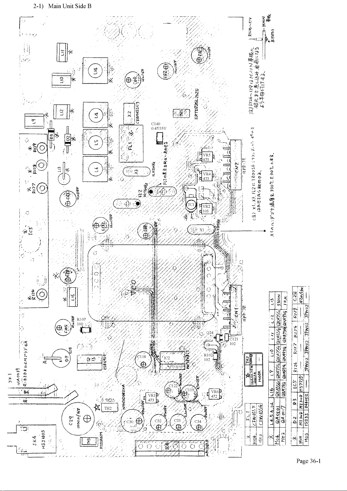
2-1) Main Unit Side B
Page 40
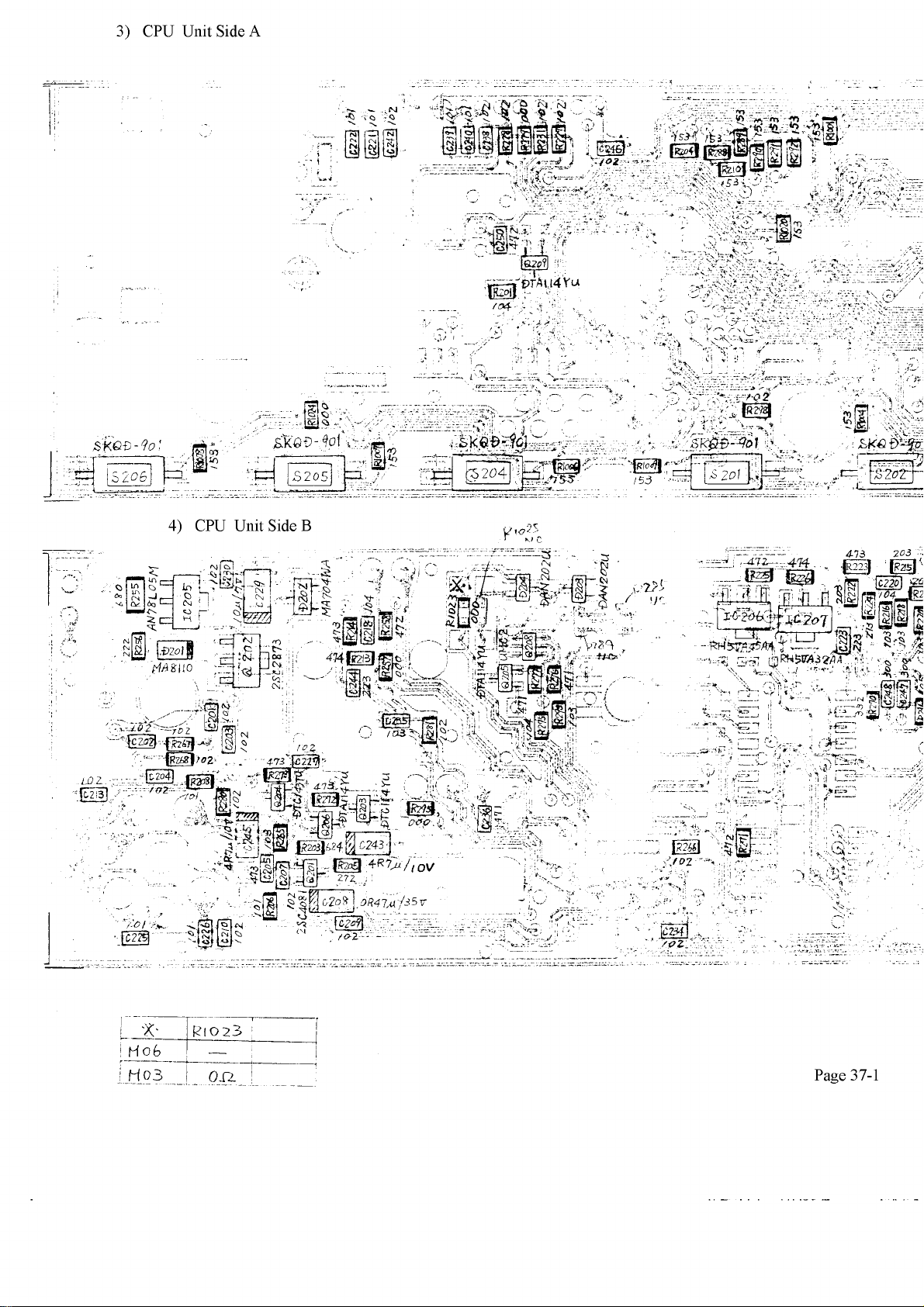
3) CPU Unit Side A
s k e v - 9 o :
¿ R , , r - -'c l
-.* - -
S205
- - • r - r :
= l , “ ' [ f i r :
;
-
- - - - -
]— ^ * f = r
153
>.-S '••' ■ - J , . j
.S
20
1
■4 . • -■
• ■' ; ■
>*• .V
.8
JM Z .
;ft2!
4) CPU Unit Side B
U\o<s
5
i ? < £ -
k ) r
'■b
t i J l
■'^V .-4- "fl ’-4
;; '^ -- -\
--TV''
; i l l ]
•v.;
j c r . t r / . ..
'i:: 3 - 'S = :> e;
i?
'■ '■ ' ■ <:.
.. j'1'5 .
’ t o z
It
/ U i i l v . ,
■ y ^ : ■
•
'•> \n
■-.'i • -• ■
'-’S'--
2
0 3
Page 41
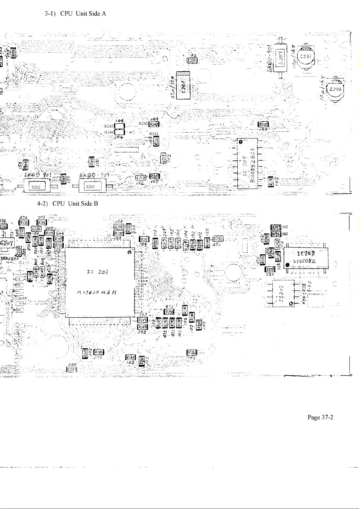
3-1) CPU Unit Side A
4-2) CPU Unit Side B
Page 37-2
Page 42

.V CN201-; 2
r ^ i é
! If-
LCD
5$ d lb d fi^
I i s f f # II
" a ! fin !
i p s j r z ^
(É1E i> ~ —"
w
s ' ^ 3 1
m !! ^
A t( !»
° § i .
c e p
r a i ; :
FP0069
' “ " s o lD e r
JK201
¡ I ^ O i S U s ® ’
m i l O 3 € l
FP0034
TT1002
6mm
PL201
PL202 \
+side
Page 37-3
w
r '
Page 43

A side
Page 38
 Loading...