

Page 1
DR-620
Service Manual
CONTENTS
SPECIFICATIONS
1) G ENE R AL.............................................................................2
2) TRAN S M IT T ER...................................................................2
3) R E CEIVER
CIR CUIT DESCRIPTION
1) VHF Reception....................................................................4
2) UHF Reception....................................................................5
3) FM Reception.......................................................................5
4) V/V (VHF-VHF) Dual Reception......................................6
5) U/U (UHF-UHF) Dual Reception
6) VHF Squelch Control
7) UHF Squelch Control.........................................................6
8) Transmit Signal Path..........................................................7
9) VHF Transmit Signal P ath.................................................7
10) UHF Transmit Signal Path.................................................7
11) VHF Tx APC Circuit............................................................7
12) UHF Tx APC Circuit............................................................8
13) VHF PTT Circuit...................................................................8
14) UHF PTT Circuit..................................................................8
15) VHF PLL................................................................................8
16) UHF PLL ................................................................................9
17) Power-on Circuit.................................................................9
SEMICONDU CTOR DATA
1) M5218FP (X A0068)......................................................... 10
2) NJM78L05UA (XA0098) ................................................. 10
3) NJM7808FA (XA0102).................................................... 10
4) TC4S66F (X A 0115)......................................................... 11
5) AN8010M (X A 0 119).........................................................11
6) BU4052BF (XA0236)....................................................... 11
7) TA75S01F (XA0332)........................................................ 12
8) TC4W 53FU (XA0348)..................................................... 12
9) TA31136FN (XA0404)..................................................... 12
10) LA4425A (XA0410).......................................................... 13
11) NJM2904V (XA0573)....................................................... 13
12) NJM2902V-TE1 (XA0596) ............................................. 13
13) S-80845ALMP-EA9-T2 (X A0620)
14) TK10931V (XA0666)........................................................ 14
...........................................................................3
....................................
.........................................................6
...............................
14
15) BR24C64F-E2 (X A 0669 )
16) LC75884W (XA 08 9 9)
17) M51132FP (XA0900)....................................................... 17
18) M30620FCAGP (XA 0913/XA0949)...................... 17~19
19) M38503M2H667FP (XA 0914)
20) M64076AGP (XA0 9 1 5)...................................................22
21) S-816A50AM C (XA0925)
22) NJM 78M05DL1A (XA 0 947)
23) Transistor, Diode, and LED Outline Drawings.... 24~25
24) LCD Connection........................................................26~27
6
EXPLODED VIE W
1) Front View
2) Bottom V iew....................................................................... 29
PARTS LIST
Front Unit.................................................................... 30~31
LED Un it..............................................................................31
Main Un it.....................................................................31~42
Mechanical Parts..............................................................42
Packing Parts.....................................................................42
Accessories (Screw S et).................................................42
ADJUSTM ENT
1) Adjustment Sp o t...............................................................43
2) Adjustment Mode..............................................................44
3) VHF Adjustment Specification.......................................45
4) UHF Adjustment Specification.....................................46
5) VHF Test Specification....................................................47
6) UHF Test Specification....................................................48
PC BOARD VIEW
1) Front Side A ........................................................................49
2) Front Side B ........................................................................49
3) Main Side A ........................................................................50
4) Main Side B ........................................................................ 51
FRONT SCHEMATIC DIA G R A M ...................................52
MAIN SCHEMATIC D IA G R A M ........................................53
FRONT B LO CK D IA G R AM ..............................................54
MAIN BLOCK DIA G R AM ...................................................55
...........................................................................28
...............................................
..................................................... 16
...............................
...............................................
..........................................
ALINCO,INC.
15
20~21
23
23
Page 2
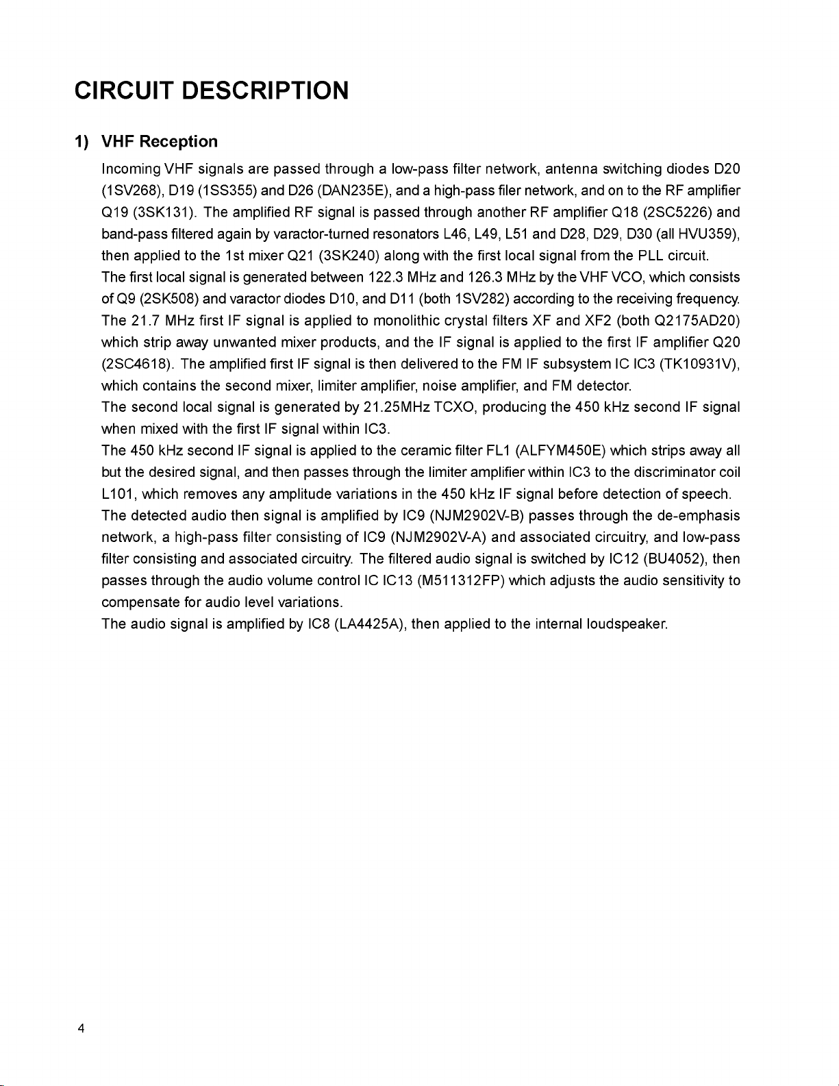
SPECIFICATIONS
1) GENERAL
Frequency coverage
DR-620T (U.S amateur)
DR-620E (European amateur)
Operating mode
Frequency resolution
Number of memory channels
Antenna impedance
Power requirement
Ground method
Current drain Receive
Transmit
Operating temperature
Frequency stability
Dimensions
Weight
87.500 - 107.995MHz (WFM RX)
108.000 - 135.995MHz (AM RX)
136.000 - 173.995MHz (RX)
144.000 - 147.995MHz (TX)
335.000 - 479.995MHz (RX)
430.000 - 449.995MHz (TX)
87.500 - 107.995MHz (WFM)
144.000 - 145.995MHz (RX, TX)
430.000 - 439.995MHz (RX, TX)
16K0F3E (Wide mode) 8K50F3E (Narrow mode)
5, 8.33, 10, 12.5, 15, 20, 25, 30, 50, 100kHz
200
50Q unbalanced
13.8V DC±15% (11.7 to 15.8V)
Negative ground
0.6A (Max.) 0.4A (Squelched)
11.0A
- 10 to 60 C
±2.5ppm
142 (w) x 40 (h) x 174 (d) mm
(w/o knobs)
Approx. 1.0kg
2) TRANSMITTER
Output power
Modulation system
Maximum frequency deviation
Spurious emission
Adjacent channel power
Modulation Distortion
Microphone impedance
2
High : 50W (VHF)
35 W(UHF)
Mid : 10W
Low : 5W
Variable reactance frequency modulation
±5kHz (Wide mode) ±2.5kHz (Narrow mode)
-60dB
-60dB
Lass than 3%
2kQ
Page 3

3) RECEIVER
Sensitivity
Receiver circuitry
Intermediate frequency
Squelch sensitivity
Selectivity (-6dB / -60dB)
Spurious and image rejection ratio
Audio output power
! Note : All specifications are subject to change without notice or obligation.
-16dBu for 12dB SINAD
Double conversion superheterodyne
1st 21.7MHz 2nd 450kHz (VHF)
1st 45.1MHz 2nd 455kHz (UHF)
-18dBu
12kHz/ 24kHz
70dB
2.0W (8Q, 10% THD)
3
Page 4
CIRCUIT DESCRIPTION
1) VHF Reception
Incoming VHF signals are passed through a low-pass filter network, antenna switching diodes D20
(1SV268), D19 (1SS355) and D26 (DAN235E), and a high-pass filer network, and on to the RF amplifier
Q19 (3SK131). The amplified RF signal is passed through another RF amplifier Q18 (2SC5226) and
band-pass filtered again by varactor-turned resonators L46, L49, L51 and D28, D29, D30 (all HVU359),
then applied to the 1st mixer Q21 (3SK240) along with the first local signal from the PLL circuit.
The first local signal is generated between 122.3 MHz and 126.3 MHz by the VHF VCO, which consists
of Q9 (2SK508) and varactor diodes D10, and D11 (both 1SV282) according to the receiving frequency.
The 21.7 MHz first IF signal is applied to monolithic crystal filters XF and XF2 (both Q2175AD20)
which strip away unwanted mixer products, and the IF signal is applied to the first IF amplifier Q20
(2SC4618). The amplified first IF signal is then delivered to the FM IF subsystem IC IC3 (TK10931V),
which contains the second mixer, limiter amplifier, noise amplifier, and FM detector.
The second local signal is generated by 21.25MHz TCXO, producing the 450 kHz second IF signal
when mixed with the first IF signal within IC3.
The 450 kHz second IF signal is applied to the ceramic filter FL1 (ALFYM450E) which strips away all
but the desired signal, and then passes through the limiter amplifier within IC3 to the discriminator coil
L101, which removes any amplitude variations in the 450 kHz IF signal before detection of speech.
The detected audio then signal is amplified by IC9 (NJM2902V-B) passes through the de-emphasis
network, a high-pass filter consisting of IC9 (NJM2902V-A) and associated circuitry, and low-pass
filter consisting and associated circuitry. The filtered audio signal is switched by IC12 (BU4052), then
passes through the audio volume control IC IC13 (M511312FP) which adjusts the audio sensitivity to
compensate for audio level variations.
The audio signal is amplified by IC8 (LA4425A), then applied to the internal loudspeaker.
4
Page 5
2) UHF Reception
Incoming UHF signals are passed through a low-pass filter network, high-pass filter network, antenna
switching diodes D16 (1SS355) and D18 (1SV268), and on to the band-pass filter network consisting
of varctor diode D49 (HVU359) and L79.
The filtered UHF signal is amplified by RF amplifier Q41 (3SK240) and fed to another band-pass filter
consisting of varactor diode D50 (HVU359) and L80, and then is passed through another RF amplifier
Q43 (2SC5226) to another band-pass filter consisting of varactor diodes D51 and D52 (both HVU359)
and L81/L82.
The amplified and filtered UHF signal is applied to the 1st mixer Q42 (3SK240) along with the first local
signal from the PLL circuit.
The first local signal is generated between 384.9 MHz and 404.9 (*2) MHz by the UHF VCO, which
consists of Q29 (2SK508) and varactor diodes D38 and D40 (both ISV278), according to the receiving
frequency.
The 45.1MHz first IF signal is applied to monolithic crystal filters XF3A and XF3B (Q4511BD10) which
strip away unwanted mixer products, and the IF signal is applied to the first IF amplifier Q44 (2SC4618).
The amplified first IF signal is then delivered to the FM IF subsystem IC IC5 (TA31136FN), which 2)
The amplified first IF signal is then delivered to the FM IF subsystem IC IC5 (TA31136FN), which
contains the second mixer, limiter amplifier, noise amplifier, and FM detector.
The second local signal is generated by 45.555 MHz crystal X4, producing the 455 kHz second IF
signal within IC5.
The 455kHz second IF signal is applied to the ceramic filter FL4 (CFW455E) which strips away all but
the desired signal, and then passes through the limiter amplifier within IC5 to the discriminator coil
L102 , which removes any amplitude variations in the 455 kHz IF signal before detection of speech.
The detected audio then signal is amplified by IC9 (NJM2902V-C) passes through the de-emphasis
network, a high-pass filter consisting of IC9 (NJM2902V-D) and associated circuitry, and a low-pass
filter consisting and associated circuitry. The filtered audio signal is switched by IC12 (BU4052), then
passes through the audio volume control IC IC13 (M511312FP), which adjusts the audio sensitivity to
compensate for audio level variations.
The audio signal is amplified by IC8 (LA4425A) then applied to the internal loudspeaker.
3) FM Reception
Incoming FM signals are passed through a low-pass filter network, antenna switching diodes D19
(1SS355), D20 (1SV2685) and D26 (DAN235E), and a high-pass filter network, and on the RF amplifier
Q36 (2SC5066). The amplified RF signal is passed through band-pass filtered L, C, then applied to
the 1st mixer Q33 (2SC5066) along with the first local signal from the circuit.
The first local signal is generated between 86.7 MH and 118.7 MHz by the FM VCO, which consists of
Q14 (2SC4808) and varactor diodes D23, and D25, (both 1SV282) according to the receiving frequency.
The 10.7 MHz first IF signal is applied to ceramic filters FL3 (SFT10.7MAS) which strip away unwanted
mixer products, and the IF signal is applied to the first IF amplifier Q37 (2SC4618). The amplified first
IF signal is then delivered to the FM IF subsystem IC IC3 (TK10931V), limiter amplifier, noise amplifier,
and FM detector.
The 10.7 MHz first IF signal is applied to the discriminator coil L53, which removes any amplitude
variations in the 10.7 MHz IF signal before detection of speech.
5
Page 6
4) V/V (VHF-VHF) Dual Reception
During V & V operation, the incoming VHF “sub” band signal is passed through a low-pass filter network,
antenna switching diode D19 (1SS355), D20 (1SV268) and a high-pass filter network to the RF amplifier
Q19 (3SK131). The amplified RF signal is passed through a high-pass filter network, VHF “sub” RF
amplifier Q31 (2SC5066), and a low-pass filter network, then is applied to the VHF “sub” first mixer
Q32 (2SC5066) along with the 45.1 MHz VHF “sub” first local signal from the VHF “sub” VCO circuit.
The VHF “sub” first local signal is generated between 189.1 MHz and 193.1 MHz by the VHF “sub”
VCO Q38.
The 45.1 MHz VHF “sub” second IF signal is applied to the UHF receiving circuit. The VHF “sub” signal
is amplified, filtered, and demodulated, etc., by the UHF “main” receiving circuit, described previously.
5) U/U (UHF-UHF) Dual Reception
During U/U operation, the incoming UHF “sub” band signal is passed through high-pass and low-pass
filter networks, antenna switching diodes D16 (1SS355) and D18 (ISV268), and another high-pass
filter network to the RF amplifier Q51 (2SC5066). The amplified RF signal is passed through a low-
pass filter network, UHF “sub ”RF amplifier Q49 (2SC5066), and low-pass filter network, then is applied
to the UHF “sub” first mixer Q52 (2SC5066) along with the 21.7 MHz UHF “sub” first local signal from
the UHF “sub” VCO.
The UHF “sub” first local signal is generated between 408.3 MHz and 428.3MHz by the UHF “sub”
VCO Q13.
The 21.7 MHz UHF “sub” second IF signal applied to VHF receiving circuit. The UHF “sub” signal is
amplified, filtered, and demodulated, etc., by the VHF receiving circuit, described previously.
6) VHF Squelch Control
When no VHF carrier is being received, noise at the output of the detector stage in IC3 is amplified and
band-pass filtered by the noise amp section of IC3, then passes through the noise adjust VR (VR8) to
CPU. The resulting DC voltage is applied to pin 88 of main CPU IC19 (M30624FGAGP), which
compares the squelch threshold level to that which set by the font panel VHF SQL knob.
While no carrier is received, pin 55 of IC19 remains “high,” turning on the squelch switch Q108
(DTC363EK) to disable audio output from the speaker.
7) UHF Squelch Control
When no UHF carrier is being received, noise at the output of the detector stage in IC5 is amplified
and band-pass filtered by the noise amp section of IC5, then passes through the noise adjust VR8 to
cpu. The resulting DC voltage is applied to pin 90 of main CPU IC19, which compares the squelch
threshold level to that which set by the front panel UHF SQL knob.
While no carrier is received, pin 56 of IC19 remains “high” turning the squelch switch Q109 (DTC363EK)
to disable audio output from the speaker.
6
Page 7
8) Transmit Signal Path
The speech signal from the microphone passes through the MIC jack CN601 to AF amplifier IC601
(M5218FP) on the FRONT UNT. The amplified speech signal is subjected to amplitude limiting by
IC601 (M5218FP), then passes through the Front interface jacks CN602 and CN2 to MAIN Unit. On
the MAIN UNIT, the speech signal passes through the audio mute switch IC7 (TC4066F), MIC gain
control VR5 and buffer amplifier IC1 (NJM2902V-C) and a low-pass filter network at IC1 (NJM2902V-
A) to deviation control VR3 (for VHF Tx audio) or VR4 (for UHF Tx audio).
9) VHF Transmit Signal Path
The adjusted speech signal from VR3 is delivered to VHF VCO Q9, which frequency modulates the
transmitting VCO D6 (1SV278).
The modulated transmit signal passes through buffer amplifier Q7 (2SC5066), a low-pass filter network,
and another buffer amplifier Q3 (2SC5226) to another low-pass filter network.
The filtered transmit signal is applied to the Pre-Drive amplifier Q2 (2SK3074) and Drive amplifier Q1
(2SK2975), then finally is amplified by Power amplifier Q4 (RD70HV1) up to 50 Watts. This three
stage power amplifier’s gain is controlled by the APC circuit.
The 50-Watt RF signal passes through a low-pass filter network, antenna switch D1 (XB15A407), and
another low-pass filter network, and then is delivered to the ANT jack.
10) UHF Transmit Signal Path
The adjusted speech signal from VR4 is delivered to UHF VCO Q29 which frequency modulates the
transmitting VCO D35 (1SV278).
The modulated transmit signal passes through buffer amplifiers Q28 (2SC5066) and Q7 (2SC5226) to
a high-pas filter network.
The filtered transmit signal is applied to the Pre-Drive amplifier Q2 (2SK3074) and Drive amplifier Q1
(2SK2975), then finally is amplified by Power amplifier Q4 (RD70HV1) up to 35 Watts. This three
stage power amplifier’s gain is controlled by the APC circuit.
The 35-Watt RF signal passes through a high-pass filter network, antenna switch D12 and D13
(UM9401F), low-pass filter and high-pass filter networks, and then is delivered to the ANT jack.
11) VHF Tx APC Circuit
A portion of the power amplifier output is rectified by D8 (MA4S713), D9 (MA4S713) and Q12 (2SC4081),
then delivered to APC IC1 (NJM2902V-D) as a DC voltage which is proportional to the output level of
the power amplifier.
The APC IC1 compares the rectified DC voltage from the power amplifier and the reference voltage
from the main CPU IC19, producing a control voltage for the Automatic Power Controller Q8 (RN2107)
and Q11 (RN1107) which regulates supply voltage to the Pre-Drive amplifier Q2, Drive amplifier Q1,
and Power amplifier Q4, so as to maintain stable output power under varying antenna loading conditions.
7
Page 8
12) UHF Tx APC Circuit
A portion of the power amplifier output is rectified by D9 (M44S713), D22 (MA4S713) and Q12
(2SC4081), then delivered to APCD ICI (NJM2902V-D) as a DC voltage which is proportional to the
output level of the power amplifier.
The APC IC1 compares the rectified DC voltage from the power amplifier and the reference voltage
from the main CPU IC19, producing a control voltage for the Automatic Power Controller Q8 (RN2107)
and Q11 (RN1107) which regulates supply voltage to the Pre-Drive amplifier Q2, Drive amplifier Q1,
and Power amplifier Q4, so as to maintain stable output power under varying antenna loading conditions.
13) VHF PTT Circuit
When the PTT switch is pressed, pin 4 of front CPU IC604 (M38503M) goes “LOW,” which sends the
“PTT” command to the main CPU, IC19. When it receives the “PTT” command, pin71 of Q19 goes
“high” to control local switch D5 (DAN235E), filter switch D2, D3, TX switch D17 (DAN235E), and APC
switch Q8/Q11, which activates the VHF Tx circuit. Meanwhile, pin 69 of IC19 goes “low,” which
disables the VHF Rx circuit.
14) UHF PTT Circuit
When the PTT switch is pressed, pin 4 of FICront CPU IC604 (M38503M) goes “LO” which sends the
“PTT” command to the main CPU, IC19, When it receives the “PTT” command, pin72 of IC19 goes
“high” to controls local switch D5, filter switch D2, D3, TX switch D17 and APC switch Q8/Q11, which
activates the UHF Tx circuit. Meanwhile, pin 70 of Q19 goes “low,” which disables the UHF Rx circuit.
15) VHF PLL
A portion of the output from the VHF VCO Q9 (2SK508) passes through buffer amplifiers Q7 (2SC5066)
and Q5 (2SC5066) to the programmable divider section of the PLL IC IC2 (M64076AGP), which
divides the frequency according to the frequency dividing data from the main CPU, IC19. It is then
sent to the phase comparator.
The 21.25 MHz frequency of the reference oscillator circuit, made up of TCXO X1, is divided by the
reference frequency divider section of IC2 into 4250 or 3400 parts to become 5 kHz or 6.25 kHz
comparative reference frequencies, which are utilized by the phase comparator.
The phase comparator section of IC2 compares the phase between the frequency-divided oscillation
frequency of the VCO circuit and comparative frequency, and its output is a pulse corresponding to the
phase difference.
This pulse is integrated by the charge pump and loop filter of IC2 into a control voltage (VCV) to
control the oscillation frequency of the VHF VCO Q9.
8
Page 9
16) UHF PLL
A portion of the output from the UHF VCO Q29 (2SK508) passes through buffer amplifier Q28 (2SC5066)
and Q39 (2SC5066) to the programmable divider section of the PLL IC IC2 (M64076AGP), which
divides the frequency according to the frequency dividing data from the main PU IC2. It is then sent to
the phase comparator.
The 21.25 MHz frequency of the reference oscillator circuit, made up of TCX0 X1, is divided by the
reference frequency divider section of IC2 into 4250 or 3400 parts to become 5 kHz or 6.25kHz
comparative reference frequencies, which are utilized by the phase comparator.
The phase comparator section of IC2 compares the phase between the frequency-divided oscillation
frequency of the VCO circuit and comparative frequency, and its output is a pulse corresponding to the
phase difference.
This pulse is integrated by the charge pump and loop filter of IC2 into a control voltage (VCV) to
control the oscillation frequency of the UHF VCO Q29.
17) Power-on Circuit
When the POWER switch is turned on, pin 18 of man CPU IC19 goes “low.” When pin 18 of IC19 goes
“low,” pin 79 of IC19 goes “high” to activate the power switches Q63 (2SB1386) and Q74 (2SC4081),
which supply the DC power to the radio.
9
Page 10
SEMICONDUCTOR DATA
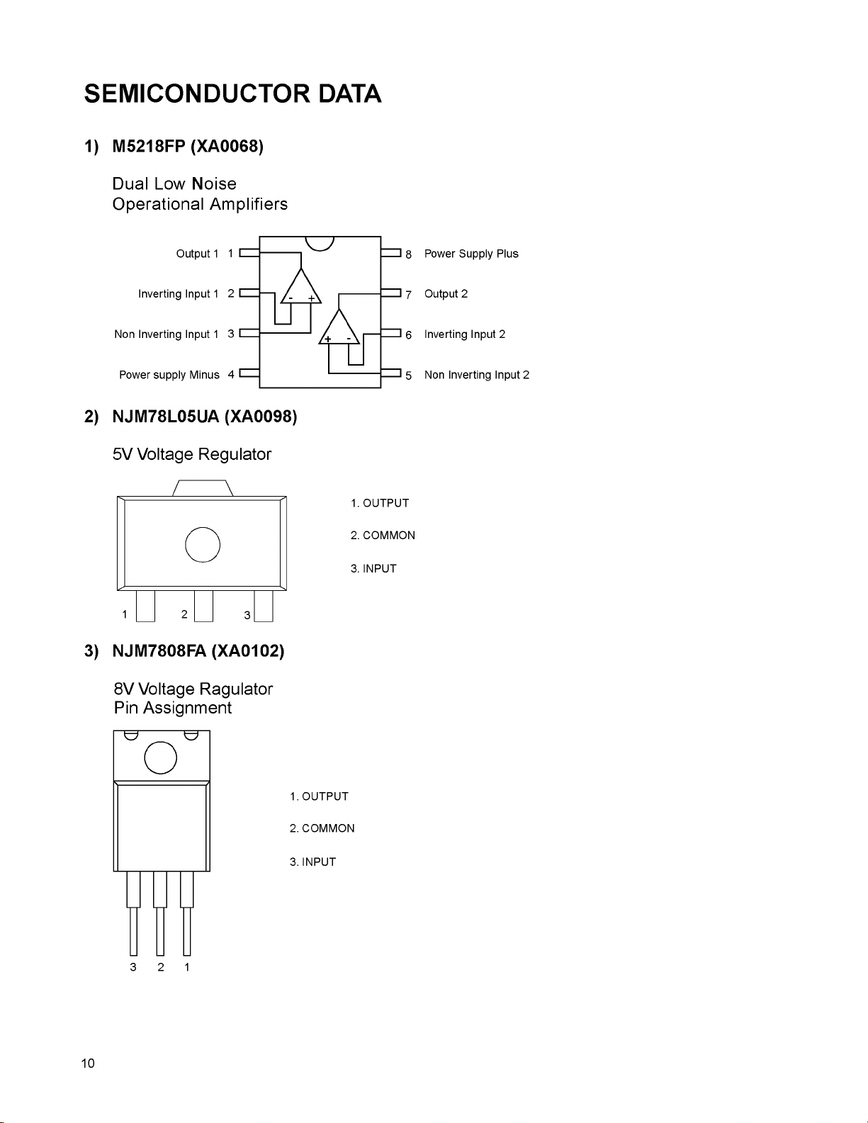
1) M5218FP (XA0068)
Dual Low Noise
Operational Amplifiers
Output 1 1
Inverting Input 1 2
Non Inverting Input 1 3
Power supply Minus 4
2) NJM78L05UA (XA0098)
5V Voltage Regulator
3) NJM7808FA (XA0102)
1. OUTPUT
2. COMMON
3. INPUT
Power Supply Plus
8
Output 2
7
Inverting Input 2
6
Non Inverting Input 2
5
8V Voltage Ragulator
Pin Assignment
3 2 1
10
1. OUTPUT
2. COMMON
3. INPUT
Page 11
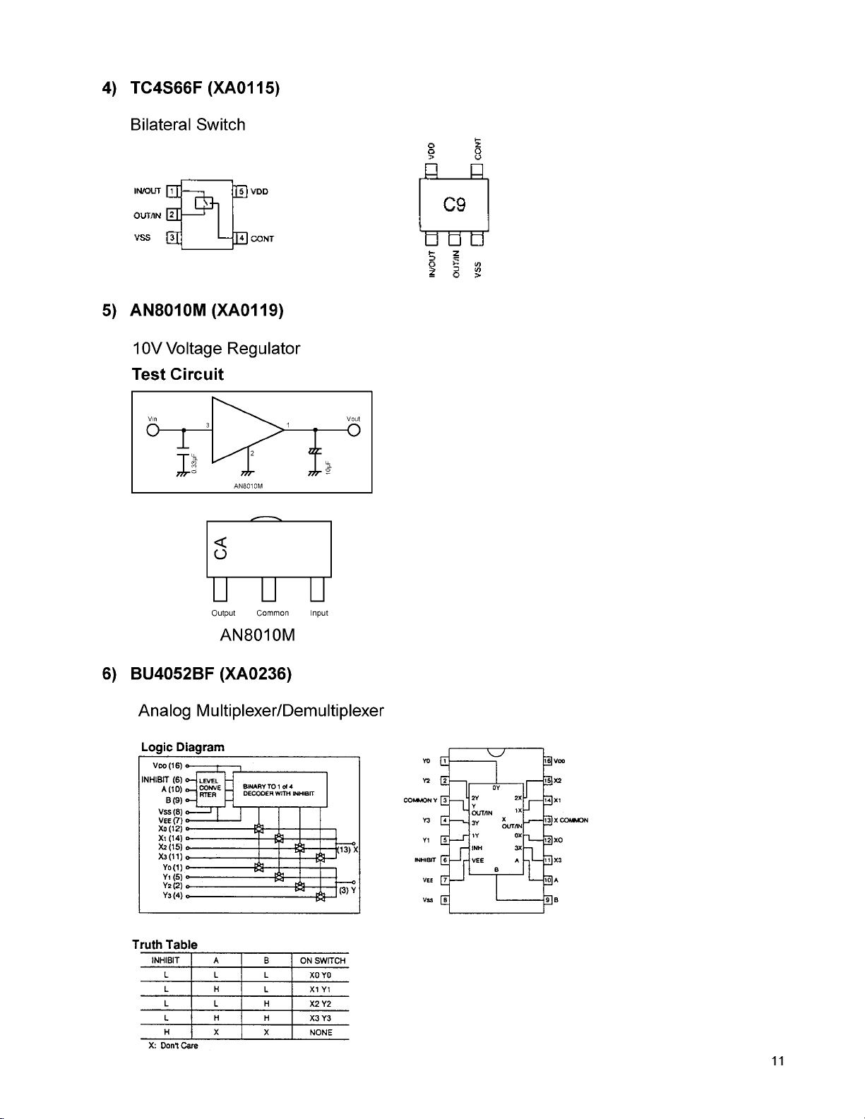
4) TC4S66F (XA0115)
Bilateral Switch
5) AN8010M (XA0119)
10V Voltage Regulator
Test Circuit
u u u
Output Common Input
AN8010M
6) BU4052BF (XA0236)
Analog Multiplexer/Demultiplexer
11
Page 12

7) TA75S01F (XA0332)
Operational Amplifiers
jg
____
a
y y y
8) TC4W53FU (XA0348)
Multiplexer/Demultiplexer
VCC OUT
Function Table
Control input
INH A
L L ch0
L H
H
* Don't Care
*
ON channel
ch1
NONE
9) TA31136FN (XA0404)
Low Power FM IF
Block Diagram
COMMON 1
INH 2 7 ch0
VEE |_3_
VSS 4 5 A
•
-P*
O i
GO
~n
8 VDD
6 | ch1
12
Page 13
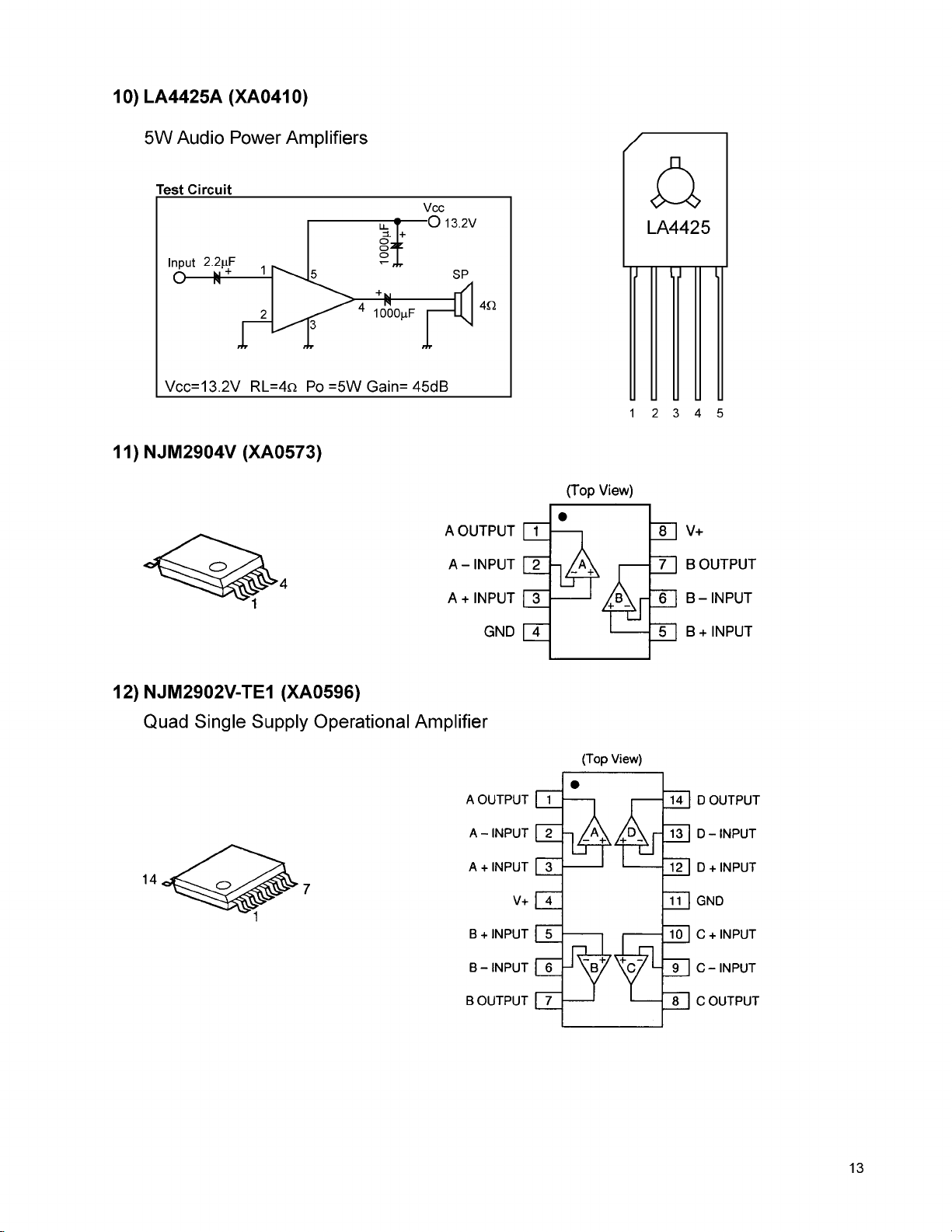
10) LA4425A (XA0410)
5W Audio Power Amplifiers
Test Circuit
11) NJM2904V (XA0573)
1 2 3 4 5
12) NJM2902V-TE1 (XA0596)
Quad Single Supply Operational Amplifier
13
Page 14
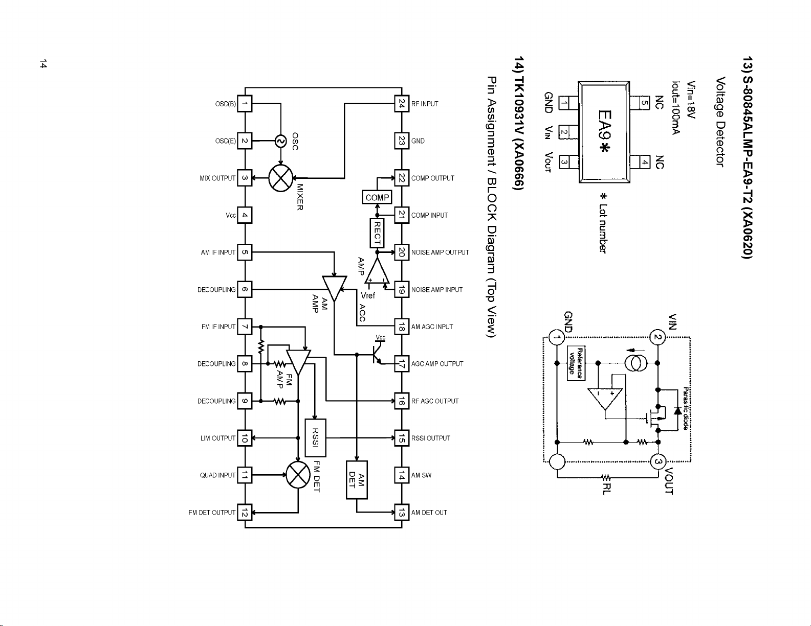
13) S-80845ALMP-EA9-T2 (XA0620)
Pin Assignment / BLOCK Diagram (Top View)
0 <
c 3
o
to
w
1 -
o
o 02
o <
3
>
X
>
o
o>
o>
o>
3
c
3
c r
(D
O
(Q
§
ST
CD
D
CD
CD
O
O
Page 15
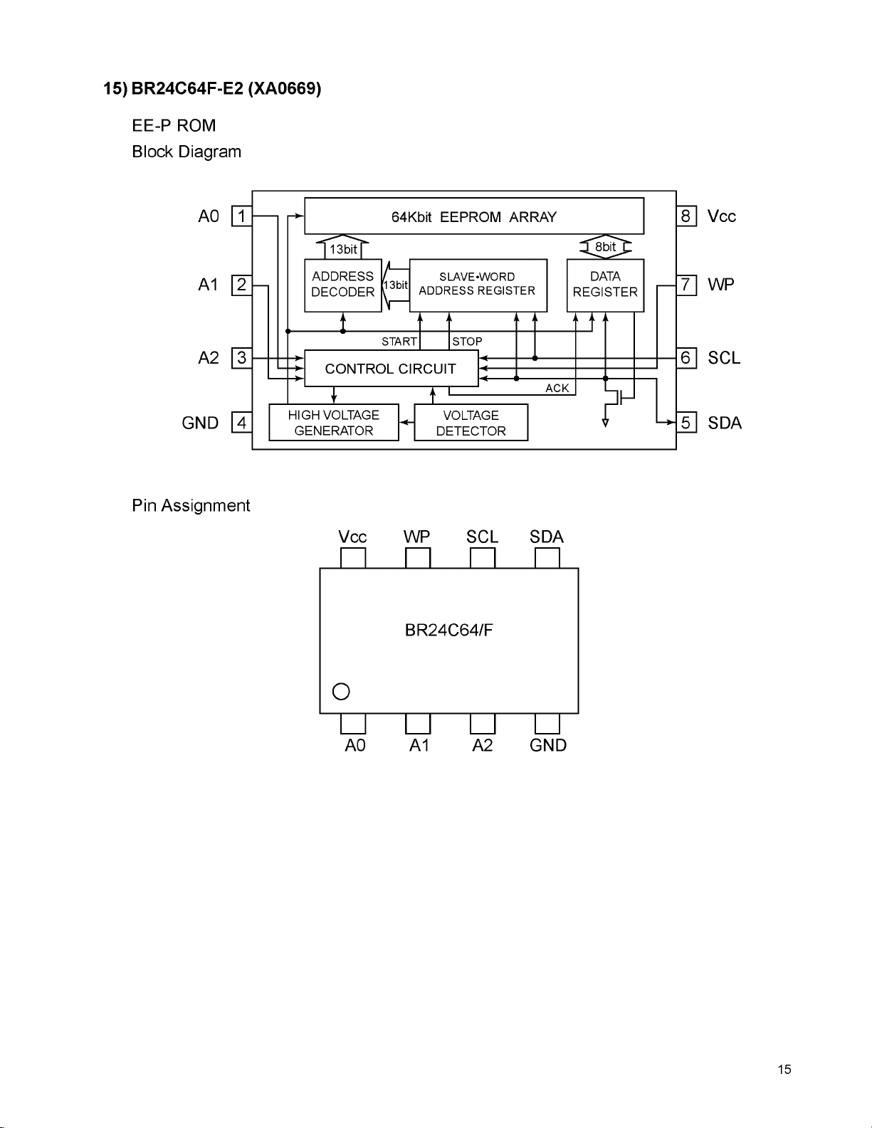
15) BR24C64F-E2 (XA0669)
EE-P ROM
Block Diagram
AO 1
A1 2
A2 3
GND 4
4
Pin Assignment
páb it
ADDRESS
DECO DER
CON TROL C IR CU IT
I
HIGH VOLTAGE
GENERATOR
Vcc WP SCL SDA
64Kbit EEP R OM ARRAY
h
13bit
N
START STOP
SLAVE^WORD
ADDRESS REGISTER
VOLTAGE
DETECTOR
ACK
DATA
REGISTER
H
r
a Vcc
7 WP
e SCL
5
5 SDA
BR24Ce4/F
O
AO A1 A2 GND
15
Page 16

16) LC75884W (XA0899)
LCD Driver
*n 'J'
in m
vt in
-c m fN ■-<
LC75884W
KS 6 \= Z 61
K I1 t = Z
K I2 C =
K I3
K I4 C =
K I5 C T!
VD D E =
VLCD 1ZZ
V L C D l C Z
VLCD2 i =
VS S EZZ
TEST 1 =
OSC C Z
RE S C Z
d o i n :
CE 1 =
CL C Z
D i c n
P l / S l c =
P 2 /S 2 c z:
in Tf fo fs h j ; £ E E f O iN H ü t n c c ^ y M n ' # ^
[/) ui tu m u O O O o m m u -u r j^ j '-î ï^ r ^ j'- ïj' ^ ’iT
i i W K K i i U U U U i O t i f l n n w w w w w u j u )
nnnnnnnnnnnnnnnnnnnn
/ fiO 50 41
70
aoO
1 10
UUUUUUUUUUUUUUUUUWLIU
■v.-^ w w M w w n t n t o w w u i u li /)
cO **
A ft
(S QFP 80 )
20
AO
t z i S 4 2
— } S4G
E = l S 3 9
30
21
S41
= Z I S 38
= ) S 3 7
“ Z I S 3 6
z n S 3 5
= 1 S 3 4
= 1 S 3 3
= J S 3 2
= ] S 3 1
= □ S 3 0
n : S 29
5 2 9
m S 2 7
^ S 2 6
= 3 £ 2 5
S24
= 3 S 2 3
Block Diagram
DO O-
D I O-
CL O-
CE O-
VD D O
VDET
h
co (N
S 2
o o
u u
O O O
COMMON
D R IVER
CLOC K
GE NERAT OR
CCB
IN T E R F A C E
SEGM EN T D R IVER & LAT CH
S H IF T REGIS T E R
CO NTROL
RE G ISTER
KE Y
KEY SCAN
^ ro CN I—)
P4 P4 Al Ai
\ \ \ \
in ^ m fN >h
co co co co co
0 0 0 0 0
BUF FER
16
Ô Ô Ô Ô Ô
in n (N h
H H H H H
« « « « «
Ô Û Ô Ô Ô Ô
vo in (*) in h
co co co co co co
« « W w U5 W
N X
in
in in
co co
Page 17

17) M51132FP (XA0900)
2ch Electronic Volume
5 !
O
1
Ref. supply out
Filter
NC
5
GND
£
Volume 1 cont.
[ T
w
K>
T I
Noise cont.
Volume 2 cont.
VCA S W
m
E
HZ
T I
18) M30620FCAGP (XA0913/XA0949)
Main CPU
? Q Q Q Q Q Q Q
'5 ^ 's i's ^ -a 's ' i; Q
QQQQQQQQ 5-
"co ^ 7?5
Q Q
K. 51
< << < << < < < ■?<<< <<<
Q Q Q
^ 1- cjIo ^ w^5 Is-
U) "(Ö N
C\JC\IC\1C\JCMC\JC\JC\IC0C0 OCOCOCOCOCOCOCO
D_Q_Q_D_Q_Q_Q_CL>Q_>CLÜ_CLCLQ_Q_Q-
1 1 L
16 Output 1
15 Input 1
VCC
1 3
NC
S I
NC
1 2
11 Input 2
H Output 2
Mode SW
S
II
CL CL
P12/D10 -
pi 1/D9 -
P-Io/Ds-
PO7/D7 -
P06/D6 *
P05/D5 -
P04/D4 -
P03/D3 *
P02/D2 -
P01/D1 -
PO0/D0 -
PIO7/AN7/KI3-
PIO6/AN6/KI2 -
P105/AN5/KM -
P104/AN4/KIO -
P103/AN3 -
PIO2/AN2 -
PIO1/AN1 -
AVss -
PIO0/AN0 '
Vref "
_____
AVcc _
P97/ADtrg/Sin4 "
P96/ANEX1/SOUT4 "
P95/ANEX0/CLK4 -
m u m u m w m
0
M30620FCAGP
O
y
^ CO
CD CD
< <
Q Q !
CD CD
Ü_ CL
oo
i dÜ
"i s5;
11— tr c0 2 O 1=1 .cmi^-i ,o n
I j 01550
¿3 Iff!X
o<!o
0- CL CL CL C
A
■ P42/A18
Ü] -
■ P43/A19
U
- P44/CS0
m
• P45/CS1
s
• P46/CS2
i -
■ P47/CS3
441 -
0
S
m •
4o1 •
m -
s -
m -
m -
0
V
___
• P50/WRL7WR
• P51/WRH/BHE
• P52/RD
' P53/BCLK
' P54/HLDA
‘ P55/HOLD
• P56/ALE
• P57/RDY/CLKOUT
■ P60/CTS0/RTS0
- P61/CLK0
• P62/RXD0
• P63/TXD0
____
’ P64/CTS1/RTS1/CLKS1
■ P65/CLK1
■ P6e/RxDi
• P67/TXD1
■ P7o/TxD2/SDA/TAOoUT(;ii)
• P7i/RxD2/SCL7TA0lN/TB5lN(ä1)
' P72/CLK2/TA1 out/V
17
Page 18

Terminal Function of Main CPU
No. Pin Name Function I/O Logic
1 P94/DA1
2 P93/DA0
3 P92
4 P91
5 P90
6 BYTE
7 CNVss
8 P87
9 P86
10 RESET
11 Xout
12
Vss
13 Xin
14
Vcc
15 P85
16 P84
17 P83
18 P82
19 P81
20 P80
21 P77
22 P76
23 P75
24 P74
25 P73
26 P72
27 P71
28 P70
29 P67
30 P66
31 P65
32 P64
33 P63
34 P62
35 P61
36 P60
37 P57
38 P56
39 P55
40 P54
41 P53
42 P52
43 P51
44 P50
45 P47
46 P46
47 P45
48 P44
49 P43
50 P42
51 P41
52 P40
53 P37
54 P36
55 P35
56 P34
TONE O D/A CTCSS tone output/DCS output
APC O D/A Power output control
DATA O Pulse Serial data output for PLL IC
STB O Pulse Strobe for PLL IC
CLK O Pulse Seriai clock output for PLL IC
BYTE I GND
CNVss I H Witer control
-
-
O
O
RESET I L Reset input
XOUT O Main clock output
VSS
XIN
VCC
-
I
-
NMI I Activ high Interruption
BU I L
SEC I
Activ high
PSW I L Power switch input
CLKS O
Activ high
MVRC O Pluse Main volume control
LAMP I L
SVRC O Pulse Sub volume control
-
O
TUV O Pulse 144MHz Tuning-voltage control
-
O
TUU O Pulse 430MHz Tuning-voltage control
RXD2 I Pulse Serial Communication port for Clone
TXD2 O Pulse Serial Communication port for Clone
TXD1 O Pulse Serial Communication port for TNC
RXD1 I Pulse Serial Communication port for TNC
SCLK O Pulse Witer control
BUSY O Pulse Witer control
TXD O Pulse Serial Communication port for Front CPU
RXD I Pulse Serial Communication port for Front CPU
SCL O Pulse Serial clock output for EEPROM
SDA I/O Pulse Serial dara output for EEPROM
DUD
I Activ low
SCR I Activ low
EPM I Activ low
PTTM I Activ low
T5 O Activ low TX power output ON/OFF
SQC O Activ low Squelch control for TNC
STBD O Pulse Strobe for Digital unit
DSQ I
TNCB O
VVCS O
UVCS O
Activ high
Activ high
Activ high
Activ high
DCSW O Activ high DCS switch
C/S O Activ low Digital/TNC mode ON/OFF
VAD O Activ high VHF digital ON/OFF
UAD O
M/S O
Activ high
Activ high
WIDE O Activ low Wide mode select
NAR O Activ low Narrow mode select
MUTV O Activ low VHF AF mute signal output
MUTU O Activ low VHF AF mute signal output
up
Description
-
-
GND
Main clock input
CPU power terminal
Backup signal detection input
Aleam(SCR) sinal input
CPU clock-shift output
Lighting color selection (H:2color)
up
Digital unit detect
up
Ready sigunal for digital unit
up
Witer control
up
PTT input for TNC
up
Squelch signal input for Digital unit
Power switch ON/OFF for TNC
VHF Main VCO ON/OFF
UHF Main VCO ON/OFF
UHF digital ON/OFF
MAIN/SUB band select
18
Page 19

5l PSS
5a
PS2
59 P3i
60
Vcc
6i P30
e2
Vss
63 P2l
64 P2e
eS P2S
ee P24
6i P2S
ea P22
e9 P2i
i0 P20
ii Pil
i2 Pi6
i3 Pi5
i4 Pi4
i5 Pi3
l6 Pi2
ii Pii
ia PiO
i9 POl
a0 P06
ai P05
a2 P04
aS P03
a4 P02
aS POi
ae POO
ai PiOl/ANl
aa Pi06/AN6
a9 Pi05/AN5
90 Pi04/AN4
91 Pi03/AN3
92 Pi02/AN2
9S PiOi/ANi
94
Avss
9S PiOO/ANO
9e Vref
9l
Avcc
9a P9l
99 P9e/ANEXi
i00 P9S/ANEXO
XBR O Activ high
O
DCSV
Activ high VHF DCS switch
XBR mute siqnal
DCSU O Activ high UHF DCS switch
VCC
-
CPU power terminal
SCRB O Activ low Power output for Aleam
VSS
-
GND
VMMT O Activ high VHF mod mute output
UMMT O Activ high UHF mod mute output
MMUT O Activ low Mic mute output
ULV I
ULU
Activ high
VHF unlock input
I Activ high UHF unlock input
AM O Activ high AM mode ON/OFF
O
Activ high
Activ high
Activ high
Activ high
Activ high
Activ high
VHF RX power ON/OFF
UHF RX power ON/OFF
VHF TX power ON/OFF
UHF TX power ON/OFF
MAIN 144MHz power OM/OFF
SUB 430MHz power ON/OFF
5RV O
SRU
STV O
STU O
14RS O
S43RS O
FMS O Activ high FM power ON/OFF
4SRS O
Si4RS O
aiRS O
5VS O
CSS O
Activ high
Activ high
Act v high
Act v high
Activ high
MAIN 430MHz power OM/OFF
SUB 144MHz power ON/OFF
Ext band power ON/OFF
5V power ON/OFF
5V power ON/OFF
ALAM O Activ low AF mute for Aleam
TB O Pulse ART/Toneburst siqnal output
BEPi O Pulse Beep sound 1 output
BEP2 O Pulse Beep sound 2 output
O
FAN O
Activ high
Air FAN power ON/OFF
SMTV I A/D VHF S-meter siqnal input
SQLV I A/D VHF noise input for squelch
SMTU I A/D UHF S-meter siqnal input
SQLU I A/D UHF noise input for squelch
TINV I A/D VHF CTCSS/DCS tone input
TINU I A/D UHF CTCSS/DCS tone input
BAT I A/D Power-supply voltage input
AVSS
-
AD converter Gnd
BPi I A/D Band plan
VREF
AVCC
-
-
AD converter ref. power
AD converter power
BP2 I Ext.Band plan
BPS I CH Band plan (L:CH)
THC I A/D PA Temperature detection
19
Page 20

19) M3B5Ü3M2H667FP (XÄÜ914)
Front CPU
20
Page 21

Terminal Function of Front CPU
No. Pin Name Function I/O Logic Description
i Vcc
2 Vref VREF
VCC
3 Avss AVSS
4 P44 PTT I Activ low PTT key input
S P43 RE1 I Pulse Dial (rotary encoder) input
e P42 UP I
l P41 DOWN I
a P40 FUNC I
Activ low
Activ low
Activ low
Key input (UP)
Key input (DOWN)
Key input (FUNC)
9 P2l SQL I Activ low Key input (SQL)
1 0 P2 e H/L I Activ low Key input (H/L)
ii P25/TxD RXD1 I Pulse Serial Communication port for Main CPU
2 P24/RxD TXD1
i
13 P23 TS/DCS I
i4 P22 MHz I
Pulse Serial Communication port for Main CPU
O
Activ low
Activ low
Key input (TS/DCS)
Key input (MHz)
iS CNVss CNVSS
ie P21 CALL I
1 l P20 BAND I
ia RESET RESET
Activ low
Activ low
Activ low Reset input
I
Key input (CALL)
Key input (BAND)
i9 Xin XIN I Pulse CPU clock input
2 0 Xout XOUT
2 1 Vss GND
2 2 Pil V/M I Activ low Key input (UP)
23 Pie RED O
24 P15 GREEN
2 S Pi4 TXLED
2 e Pi3 MRLED
2 l Pi2 SRLED
2 a P11 DIM1 O
29 P10 DIM2 O
O
Activ high Lighting color ON/OFF (RED)
Activ high
O
Activ high TX LED ON/OFF
O
Activ high MAIN RX LED ON/OFF
O
O Activ high
Activ high
Activ high
CPU clock output
Lighting color ON/OFF (YELLOW)
SUB RX LED ON/OFF
Dommer control 1
Dimmer control 2
30 POl
31 P06
32 P05 DO I Pulse Data input for LCD driver IC
33 P04 CE O
Activ high
Strobe for LCD driver IC
34 P03 CL O Pulse Clock output for LCD driver IC
35 P02 DI O Pulse Data output for LCD driver IC
36 P01 MUTE
O Activ high
-
3l P00 RE2 I Dial (rotary encoder) input
3a P34/AN4
39 P33/AN3
40 P32/AN2
4i P31/AN1 MVR I A/D MAIN volume voltage input
42 P30/AN0 SVR I A/D SUB volume voltage inpput
21
Page 22

2Ü) M64Ü76ÄGP (XÄÜ915)
Dual PLL Synthesizer
XBo
SI
CPS
RST
Vcc
Fini
Lockl
Pd1
VT1
VF
1
□
2 19
□
3 18
□
4
□
5
□
6
□
7 14
□
8 13
□
9
□
10 11
□
Equivalent Circuit
Fin2(Í5)
--------
SW
s
o>
o
>1
O)
"Ö
[a MP~>»
SW
20
□
□
□
17
□
16
□
15
□
□
□
12
□
□
GND
Xin
Xout
OP2
OP1
Fin2
Lock2
PD2
VT2
GND
1/64, 65
2 modules
prescaler
Parameter Symbol Condition Min. Typ. Max. Unit
Power supply voltage Vcc
Fin=a0~520MHz
Vin=-10dBm
2.l 5.5 V
LPF supply voltage VF
Local oscillator input level Vin
Local oscillator input frequency Fin
Fin=a0~520MHz
Vin=-20~-4dBm
Vcc=2.l~5.5V
-20 -4 dBm
80 520 MHz
Vcc=2.l~5.5V
Xin input level Vxin
Xin input frequency Fxin
Fxin=10~25MHz
Sine wave
Vcc=2.l~5.5V
Vxin=0.4~1.4Vp-p
0.4 1.4
10 25 MHz
Data latch (17bit)
Local 2
programmable divider
Data latch (16bit)
9 12 V
Vp-p
XBo (T )
Xout (18)-
X in ^ i)-
Fin 1(6 i—
s i® -
I
CPS(3)-
-----
<^M P
SW
osc
SW
1/64, 65
2 modulus
prescaler
21 bit shift resistor
21 bit pulse counter
1/2
divider
"( d )"
RST
Reference frequency 2
programmable divider
Reference frequency 1
programmable divider
Data latch (16bit)
Local 1
programmable divider
Data latch (17bit) —
Data latch (6bit)
Latch
selector
GND
BU£>
------
(ij)G ND
(¡7)0 P 2
22
Page 23

21) S-816A50AMC (XA0925)
Voltage Regulator
Top View
5 4
a
___
a
□ □ □
1 2 3
No. Terminal
1 EXT
2 VSS
3 ON/OFF
4 VIN
5 VOUT
22) NJM78M05DL1A (XA0947)
S X
Voltage Regulator
1.INPUT
2.GND
3.OUTPUT
23
Page 24

23) Transistor, Diode, and LED Outline Drawings
24
Page 25

RD70VHF1 (XE0047)
Nch MOS FET
ABSO LUTE MAXIMUM RATING
Symbol Test conditions Rating Unit
Pch Tc=25°C 150 W
VDS S Vgs=0V 30 V
VGSS Vds=0V ±20 V
Tj
Tstg -4 0 ~ +125 °C
ELECTRICAL C HARA C TERISTIC(Ta=25°C )
Parameter Symbol Test conditions
Saturated drain current IDSS Vds=17V, Vgs=0V 300
Gate to source leakage current IGSS Vds=10V, Vgs= 0V 5
Threshold voltage Vth Vds=12V, Ids=1ma 1.3 2.3
Output power 1 Po1 f=175 M Hz, P in=6W
Drain officiency 1 n D i 55
Output power 2 Po2
Drain officiency 2 nD2 50
Vds=12.5V
Ids(idle)=2.0A
f= 520M Hz, P in=10W
Vds=12.5V
Ids(idle)=2.0A
+175 °C
Limits
Min Max
70
50
Unit
|jA
|jA
V
W
%
W
%
25
Page 26

24) LCD Connection
26
Page 27

COM1 COM2 COM3 COM4
S1
S2
S3
S4
S5
S6
S7
SB
S9
10 k 10 l 10 h 10 p
10 a 10 b 1 0 c W-2
11 1 k 11 l 11 h
11 a 11 b 1 1 c W-3
12 k 12 l 12 h 12 p
12 a 12 b 1 2 c DP2
13k
13l 13h 13p
13a 13b 13c W-4
14k 14l 14h 14p
S10 14a 14b 14c W-5
S11
15k 15l 15h 15p
S12 15a 15b 15c
COM4
COM3
COM2
COM1 COM1
S13 Q2 R
S14
- - -
- -
-
COM2
- - -
15j
15g 15m 15n
COM4
COM3
- -
Q5
S15 Q4 15f 15e 15d
S16
S17
S1B
S19
S20
S21 Q1
14j 14g 14m 14n
TNC 14f 14e
13j
Q3
12 j
13g 13m 13n
13f 13e 13d
12 g 12 m 12 n
12f 1 2e 1 2d
S22 11 j 11 g 1 1 m 11 n
S23
SUB
11f 1 1e 1 1d
S24 10 j 10 g 1 0 m 10 n
S25 DCS
S26 T
S27 9j
10f 1 0e 1 0d
SQ
9g
BUSY-2
9m 9n
S2B minus(-) 9f 9r 9r
S29 Bj Bg Bm Bn
S30 plus(+)
Bf Be Be
S31 7j 7g 7m 7n
S32 Nar 7f 7e 7e
S33
S34
6 j 6 g 6 m 6 n
Lo 6 f 6 e 6 e
S35 5j 5g 5m
S36 Mj 5f 5e 5e
S37 4j 4g 4m 4n
S3B AM 4f 4e 4d
S39 3a
3f 3e 3d
S40 2 a 2 f 2 e 2 d
S41 F 1b,c
SQL
BUSY-1
S42 2 b 2 g 2 c T-1
S43 3b 3g 3c T-2
S44 4k 4l 4h
S45 4a 4b 4c T-3
S46 5k 5l 5h 5p
S47
S4B 6 k
5a 5b 5c T-4
6 l 6 h 6 p
S49 6 a 6 b 6 c DP1
S50 7k 7l 7h 7p
S51 7a 7b 7c T-5
S52 Bk Bl Bh Bp
S53 Ba Bb
Bc T-6
S54 9k 9l 9h 9p
S55 9a 9b 9c 5-1
S56 N.C.
- - -
11 p
5-2
-
-
14d
W-1
5n
4p
27
Page 28

EXPLODED VIEW
1) Front View
28
Page 29

2) Bottom View
AA0050
29
Page 30

PARTS LIST
Front Unit
Ref.
Parts No. Description Parts Name
No.
C601 CU3535 Chip C. GRM36B102K50PT 1 1
C602 CS0424 Chip Tantalum TMCMA1C106MTR 1 1
C603 CU3523 Chip C. GRM36CH101J50PT 1 1
C604 CU0108 Chip C. LMK212BJ105KG 1 1
C605 CU3551 Chip C. GRM36B223K16PT 1 1
C606 CU3535 Chip C. GRM36B102K50PT 1 1
C607 CS0424 Chip Tantalum TMCMA1C106MTR 1 1
C608 CU3535 Chip C. GRM36B102K50PT 1 1
C609 CU0108 Chip C. LMK212BJ105KG 1 1
C610 CU3535 Chip C. GRM36B102K50PT 1 1
C611 CU3535 Chip C. GRM36B102K50PT 1 1
C612 CU3535 Chip C. GRM36B102K50PT 1 1
C613 CU3535 Chip C. GRM36B102K50PT 1 1
C614 CU3535 Chip C. GRM36B102K50PT 1 1
C615 CS0424 Chip Tantalum TMCMA1C106MTR 1 1
C616 CU3535 Chip C. GRM36B102K50PT 1 1
C617 CS0424 Chip Tantalum TMCMA1C106MTR 1 1
C618 CU3533 Chip C. GRM36B681K50PT 1 1
C619 CU3535 Chip C. GRM36B102K50PT 1 1
C620 CU3535 Chip C. GRM36B102K50PT 1 1
C621 CU3535 Chip C. GRM36B102K50PT 1 1
C622 CU3535 Chip C. GRM36B102K50PT 1 1
C623 CU3543 Chip C. GRM36B472K25PT 1 1
C624 CU3543 Chip C. GRM36B472K25PT 1 1
C625 CU3551 Chip C. GRM36B223K16PT 1 1
C626 CU3023 Chip C. C1608CH1H101JT-AS 1 1
C627 CU3023 Chip C. C1608CH1H101JT-AS 1 1
CN601 UE0035 Connector FM214-8SMPY 1
CN602 UJ0052 Jack HJC0163-01-022 1
CN603 UE0456 Connector PI28A08M 1 1
D601 XD0254 Chip Diode 1SS355 TE17 1 1
D606 XD0254 Chip Diode 1SS355 TE17 1 1
D611 XL0069 Chip LED FA1111C-TR 1 1
D612 XL0091 Chip LED FY1111C-433-TR 1 1
D613 XL0069 Chip LED FA1111C-TR 1 1
D614 XL0092 LED MPG3338S 1 1
D618 XL0051 LED VRPG3312X 1 1
D620 XD0254 Chip Diode 1SS355 TE17 1 1
IC601 XA0068 IC M5218AFP/600E 1 1
IC602 XA0947 IC NJM78M05DL1A-TE1 1 1
IC603 XA0899 IC LC75884W 1 1
IC604 XA0914 IC M38503M2H667FP 1 1
LCD60 EL0054 LCD LCD DR620 1 1
Q601 XT0095 Chip Transistor 2SC4081 T106R 1 1
Q602 XT0095 Chip Transistor 2SC4081 T106R 1 1
Q603 XU0193 Chip Transistor RN1107 TE85L 1 1
Q604 XT0095 Chip Transistor 2SC4081 T106R 1 1
Q605 XU0193 Chip Transistor RN1107 TE85L 1 1
Q606 XU0192 Chip Transistor RN2107 TE85L 1 1
Q607 XU0173 Chip Transistor DTD114EK-T146 1 1
Q608 XU0173 Chip Transistor DTD114EK-T146 1 1
Q609 XT0095 Chip Transistor 2SC4081 T106R 1 1
Q610 XU0193 Chip Transistor RN1107 TE85L 1 1
Q611 XT0095 Chip Transistor 2SC4081 T106R 1 1
Q612 XU0193 Chip Transistor RN1107 TE85L 1 1
R601 RK3566 Chip R. ERJ2GEJ224X 1 1
R602 RK3550 Chip R. ERJ2GEJ103X 1 1
R603 RK3551 Chip R. ERJ2GEJ123X 1 1
Qty
(T)
Ref.
(E)
Parts No. Description Parts Name
No.
R604 RK3538 Chip R. ERJ2GEJ102X 1 1
R605 RK3560 Chip R. ERJ2GEJ683X 1 1
R606 RK3543 Chip R. ERJ2GEJ272X 1 1
R607 RK3550 Chip R. ERJ2GEJ103X 1 1
R608 RK3550 Chip R. ERJ2GEJ103X 1 1
R609 RK3538 Chip R. ERJ2GEJ102X 1 1
R610 RK3550 Chip R. ERJ2GEJ103X 1 1
R611 RK3550 Chip R. ERJ2GEJ103X 1 1
R612 RK3526 Chip R. ERJ2GEJ101X 1 1
R613 RK3522 Chip R. ERJ2GEJ470X 1 1
R614 RK3501 Chip R. ERJ2GE0R00X 1 1
R615 RK3546 Chip R. ERJ2GEJ472X 1 1
R616 RK3550 Chip R. ERJ2GEJ103X 1 1
R617 RK3546 Chip R. ERJ2GEJ472X 1 1
R618 RK3550 Chip R. ERJ2GEJ103X 1 1
R619 RK3550 Chip R. ERJ2GEJ103X 1 1
R620 RK3550 Chip R. ERJ2GEJ103X 1 1
R621 RK3550 Chip R. ERJ2GEJ103X 1 1
R622 RK3550 Chip R. ERJ2GEJ103X 1 1
R623 RK3550 Chip R. ERJ2GEJ103X 1 1
R624 RK3550 Chip R. ERJ2GEJ103X 1 1
R625 RK3550 Chip R. ERJ2GEJ103X 1 1
R626 RK3550 Chip R. ERJ2GEJ103X 1 1
R627 RK3550 Chip R. ERJ2GEJ103X 1 1
R628 RK3550 Chip R. ERJ2GEJ103X 1 1
R629 RK3550 Chip R. ERJ2GEJ103X 1 1
R630 RK3546 Chip R. ERJ2GEJ472X 1 1
R631 RK3550 Chip R. ERJ2GEJ103X 1
R632 RK3542 Chip R. ERJ2GEJ222X 1
R633 RK3526 Chip R. ERJ2GEJ101X 1 1
R634 RK3526 Chip R. ERJ2GEJ101X 1 1
R635 RK3558 Chip R. ERJ2GEJ473X 1 1
R636 RK3538 Chip R. ERJ2GEJ102X 1 1
R637 RK3538 Chip R. ERJ2GEJ102X 1 1
R639 RK3026 Chip R. MCR03EZHJ101 1 1
R640 RK3550 Chip R. ERJ2GEJ103X 1 1
R641 RK3570 Chip R. ERJ2GEJ474X 1 1
R642 RK3538 Chip R. ERJ2GEJ102X 1 1
R643 RK3574 Chip R. ERJ2GEJ105X 1 1
R645 RK3030 Chip R. MCR03EZHJ221 1 1
R646 RK3534 Chip R. ERJ2GEJ471X 1 1
R651 RK3530 Chip R. ERJ2GEJ221X 1 1
R652 RK3530 Chip R. ERJ2GEJ221X 1 1
R653 RK3535 Chip R. ERJ2GEJ561X 1 1
R654 RK3535 Chip R. ERJ2GEJ561X 1 1
R655 RK3528 Chip R. ERJ2GEJ151X 1 1
R656 RK3535 Chip R. ERJ2GEJ561X 1 1
R657 RK3528 Chip R. ERJ2GEJ151X 1 1
R658 RK3550 Chip R. ERJ2GEJ103X 1 1
R659 RK3550 Chip R. ERJ2GEJ103X 1 1
R660 RK3026 Chip R. MCR03EZHJ101 1 1
R661 RK3538 Chip R. ERJ2GEJ102X 1 1
R662 RK3030 Chip R. MCR03EZHJ221 1 1
R663 RK3538 Chip R. ERJ2GEJ102X 1 1
R666 RK3538 Chip R. ERJ2GEJ102X 1 1
R667 RK3538 Chip R. ERJ2GEJ102X 1 1
R668 RK3538 Chip R. ERJ2GEJ102X 1 1
R669 RK3538 Chip R. ERJ2GEJ102X 1 1
Qty
(E)
(T)
30
Page 31

Ref.
Parts No. Description Parts Name
No.
RE601 UR0015 Dial RH90N74E20-A90770 1 1
SW601 UU0015Z Switch EVQPPPA25 1 1
SW602 UU0015Z Switch EVQPPPA25 1 1
SW603 UU0015Z Switch EVQPPPA25 1 1
SW604 UU0015Z Switch EVQPPPA25 1 1
SW605 UU0015Z Switch EVQPPPA25 1 1
SW606 UU0015Z Switch EVQPPPA25 1 1
SW607 UU0015Z Switch EVQPPPA25 1 1
SW608 UU0015Z Switch EVQPPPA25 1 1
SW609 UU0015Z Switch EVQPPPA25 1
VR601 RV0035 Variable R. EVUF2JFK4B14 1 1
VR602 RV0035 Variable R. EVUF2JFK4B14 1 1
X601 XB0029 Ceramic OSC EF0S4914E5 1 1
TL0029 DIFFUSION SHEET 1 1
FG0358 LCD CUSHION DR620
ST0081 LCD HOLDER DR620 1 1
DG0041 LCD LIGHT DR620 1 1
FG0352 LCD RUBBER CONNECTOR 1 1
FM0034 MIC GND PLATE 1 1
FP0034 MIC SPACER DR110 1 1
TL0028 REFLECTIVE SHEET 1 1
Qty
(T)
LED Unit
Ref.
Parts No. Description Parts Name
No.
D602 XL0077 Chip LED FA1111C-732-TR 1 1
D603 XL0077 Chip LED FA1111C-732-TR 1 1
D604 XL0077 Chip LED FA1111C-732-TR 1 1
D605 XL0091 Chip LED FY1111C-433-TR 1 1
D607 XL0077 Chip LED FA1111C-732-TR 1 1
D608 XL0091 Chip LED FY1111C-433-TR 1 1
D609 XL0077 Chip LED FA1111C-732-TR 1 1
D610 XL0077 Chip LED FA1111C-732-TR 1
D615 XL0091 Chip LED FY1111C-433-TR 1
D616 XL0091 Chip LED FY1111C-433-TR 1 1
D617 XL0091 Chip LED FY1111C-433-TR 1 1
D619 XL0091 Chip LED FY1111C-433-TR 1 1
R647 RK3028 Chip R. MCR03EZHJ151 1 1
R648 RK3028 Chip R. MCR03EZHJ151 1 1
R649 RK3028 Chip R. MCR03EZHJ151 1 1
R650 RK3026 Chip R. MCR03EZHJ101 1 1
R664 RK3026 Chip R. MCR03EZHJ101 1 1
R665 RK3026 Chip R. MCR03EZHJ101 1 1
Qty
(T)
Main Unit
Ref.
Parts No. Description Parts Name
No.
C1 CU3035 Chip C. C1608JB1H102KT-AS 1 1
C3 CU3535 Chip C. GRM36B102K50PT 1 1
C4 CU3031 Chip C. C1608JB1H471KT-AS 1 1
C5 CU4008 Chip C. GRM42-6CH070D500PT 1 1
C6 CU3019 Chip C. C1608CH1H470JT-AS 1
C8 CU3035 Chip C. C1608JB1H102KT-AS 1 1
C9 CU7046 Chip C. UC232H0270C-T 1 1
C10 CU3035 Chip C. C1608JB1H102KT-AS 1 1
C11 CU3035 Chip C. C1608JB1H102KT-AS 1 1
C12 CU3057 Chip C. C1608CH1H130JT-A 1 1
C13 CU3057 Chip C. C1608CH1H130JT-A 1 1
Qty
(T)
Ref.
Parts No. Description Parts Name
(E)
(E)
(E)
No.
C14 CU4023 Chip C. GRM42-6CH101J500PT 1 1
C15 CU7052 Chip C. UC232H0820F-T 1 1
C16 CU3507 Chip C. GRM36CH060D50PT 1 1
C17 CU3018 Chip C. C1608CH1H390JT-AS 1 1
C18 CU3535 Chip C. GRM36B102K50PT 1 1
C19 CU3535 Chip C. GRM36B102K50PT 1 1
C20 CU4023 Chip C. GRM42-6CH101J500PT 1 1
C21 CU3535 Chip C. GRM36B102K50PT 1 1
C22 CU3511 Chip C. GRM36CH100D50PT 1 1
C23 CU3035 Chip C. C1608JB1H102KT-AS 1 1
C26 CU3535 Chip C. GRM36B102K50PT 1 1
C27 CU3515 Chip C. GRM36CH220J50PT 1 1
C29 CU3515 Chip C. GRM36CH220J50PT 1 1
C30 CU3535 Chip C. GRM36B102K50PT 1 1
C31 CU3535 Chip C. GRM36B102K50PT 1 1
C32 CU3024 Chip C. C1608CH1H121JT-AS 1 1
C33 CU3024 Chip C. C1608CH1H121JT-AS 1 1
C35 CU4016 Chip C. GRM42-6CH270J500PT 1 1
C36 CU4015 Chip C. GRM42-6CH220J500PT 1 1
C38 CU4016 Chip C. GRM42-6CH270J500PT 1 1
C39 CU4014 Chip C. GRM42-6CH180J500PT 1 1
C40 CU7050 Chip C. UC232H0560F-T 1 1
C42 CU3513 Chip C. GRM36CH150J50PT 1 1
C43 CU3518 Chip C. GRM36CH390J50PT 1 1
C44 CU3515 Chip C. GRM36CH220J50PT 1 1
C45 CU3035 Chip C. C1608JB1H102KT-AS 1 1
C46 CU3001 Chip C. C1608CH1H0R5CT-AS 1 1
C48 CU3001 Chip C. C1608CH1H0R5CT-AS 1 1
C49 CU4013 Chip C. GRM42-6CH150J500PT 1 1
C51 CU3511 Chip C. GRM36CH100D50PT 1 1
C52 CU0108 Chip C. LMK212BJ105KG 1 1
C53 CU0108 Chip C. LMK212BJ105KG 1 1
C54 CU3035 Chip C. C1608JB1H102KT-AS 1 1
C55 CU3515 Chip C. GRM36CH220J50PT 1 1
C56 CU3511 Chip C. GRM36CH100D50PT 1 1
C57 CU4011 Chip C. GRM42-6CH100J500PT 1
C57 CU4012 Chip C. GRM42-6CH120J500PT 1
C58 CU3509 Chip C. GRM36CH080D50PT 1 1
C59 CU3510 Chip C. GRM36CH090D50PT 1 1
C60 CU3514 Chip C. GRM36CH180J50PT 1 1
C61 CU3514 Chip C. GRM36CH180J50PT 1 1
C62 CE0339 Electrolytic C. 16MV 10SWB+TS 1 1
C63 CU4015 Chip C. GRM42-6CH220J500PT 1 1
C64 CU3535 Chip C. GRM36B102K50PT 1 1
C65 CS0424 Chip Tantalum TMCMA1C106MTR 1 1
C66 CU3503 Chip C. GRM36CK020C50PT 1 1
C67 CU3535 Chip C. GRM36B102K50PT 1 1
C68 CU3019 Chip C. C1608CH1H470JT-AS 1 1
C69 CU3530 Chip C. GRM36B391K50PT 1 1
C70 CE0339 Electrolytic C. 16MV 10SWB+TS 1 1
C71 CU3011 Chip C. C1608CH1H100DT-AS 1 1
C72 CU3012 Chip C. C1608CH1H120JT-AS 1 1
C73 CU3015 Chip C. C1608CH1H220JT-AS 1 1
C74 CU3035 Chip C. C1608JB1H102KT-AS 1 1
C75 CU3514 Chip C. GRM36CH180J50PT 1 1
C76 CU3514 Chip C. GRM36CH180J50PT 1 1
C78 CU3531 Chip C. GRM36B471K50PT 1 1
C79 CU3535 Chip C. GRM36B102K50PT 1 1
C80 CU3535 Chip C. GRM36B102K50PT 1 1
C81 CU3511 Chip C. GRM36CH100D50PT 1 1
C82 CU3547 Chip C. GRM36B103K16PT 1 1
C83 CU3535 Chip C. GRM36B102K50PT 1 1
C84 CU3035 Chip C. C1608JB1H102KT-AS 1 1
C85 CU3035 Chip C. C1608JB1H102KT-AS 1 1
Qty
(E)
(T)
31
Page 32

Ref.
Parts No. Description Parts Name
No.
C86 CU3535 Chip C. GRM36B102K50PT 1 1
C87 CU3035 Chip C. C1608JB1H102KT-AS 1 1
C88 CU3035 Chip C. C1608JB1H102KT-AS 1 1
C89 CU3111 Chip C. C1608JB1C104KT-N 1 1
C91 CU3502 Chip C. GRM36CK010C50PT 1 1
C92 CU3547 Chip C. GRM36B103K16PT 1 1
C93 CU3035 Chip C. C1608JB1H102KT-AS 1 1
C94 CU3511 Chip C. GRM36CH100D50PT 1 1
C95 CU3111 Chip C. C1608JB1C104KT-N 1 1
C96 CU3035 Chip C. C1608JB1H102KT-AS 1 1
C97 CU3535 Chip C. GRM36B102K50PT 1 1
C98 CS0220 Chip Tantalum TMCMA1C225MTR 1 1
C99 CU3035 Chip C. C1608JB1H102KT-AS 1 1
C100 CU3035 Chip C. C1608JB1H102KT-AS 1 1
C101 CU3535 Chip C. GRM36B102K50PT 1 1
C102 CU3506 Chip C. GRM36CH050C50PT 1 1
C103 CU4019 Chip C. GRM42-6CH470J500PT 1 1
C104 CS0220 Chip Tantalum TMCMA1C225MTR 1 1
C105 CU3512 Chip C. GRM36CH120J50PT 1 1
C106 CU4008 Chip C. GRM42-6CH070D500PT 1 1
C107 CU3551 Chip C. GRM36B223K16PT 1 1
C108 CU3035 Chip C. C1608JB1H102KT-AS 1 1
C109 CU3535 Chip C. GRM36B102K50PT 1 1
C110 CU3547 Chip C. GRM36B103K16PT 1 1
C111 CU0002 Chip C. C2012CH1H010CT-A 1 1
C112 CU4006 Chip C. GRM42-6CH050C500PT 1 1
C113 CU3502 Chip C. GRM36CK010C50PT 1 1
C114 CS0063 Chip Tantalum TMCSA1V104MTR 1 1
C115 CU3004 Chip C. C1608CH1H030CT-AS 1
C115 CU3005 Chip C. C1608CH1H040CT-AS 1
C116 CU4010 Chip C. GRM42-6CH090D500PT 1
C117 CU4007 Chip C. GRM42-6CH060D500PT 1
C118 CU3547 Chip C. GRM36B103K16PT 1 1
C119 CE0420 Electrolytic C. 16MV22SZ 1 1
C120 CU3535 Chip C. GRM36B102K50PT 1 1
C121 CU3535 Chip C. GRM36B102K50PT 1 1
C122 CU3535 Chip C. GRM36B102K50PT 1 1
C123 CU3035 Chip C. C1608JB1H102KT-AS 1 1
C124 CU4006 Chip C. GRM42-6CH050C500PT 1 1
C125 CU4001 Chip C. GRM42-6CK010C500PT 1 1
C126 CU4007 Chip C. GRM42-6CH060D500PT 1 1
C127 CU4005 Chip C. GRM42-6CH040C500PT 1 1
C128 CU3511 Chip C. GRM36CH100D50PT 1 1
C129 CU3001 Chip C. C1608CH1H0R5CT-AS 1 1
C130 CU3001 Chip C. C1608CH1H0R5CT-AS 1 1
C131 CU4019 Chip C. GRM42-6CH470J500PT 1 1
C132 CU3535 Chip C. GRM36B102K50PT 1 1
C133 CU3035 Chip C. C1608JB1H102KT-AS 1 1
C134 CU3035 Chip C. C1608JB1H102KT-AS 1 1
C135 CS0063 Chip Tantalum TMCSA1V104MTR 1 1
C136 CU3531 Chip C. GRM36B471K50PT 1 1
C137 CU3535 Chip C. GRM36B102K50PT 1 1
C138 CU3523 Chip C. GRM36CH101J50PT 1 1
C139 CU3035 Chip C. C1608JB1H102KT-AS 1 1
C141 CU3035 Chip C. C1608JB1H102KT-AS 1 1
C142 CU3523 Chip C. GRM36CH101J50PT 1 1
C143 CU3035 Chip C. C1608JB1H102KT-AS 1 1
C144 CU3035 Chip C. C1608JB1H102KT-AS 1 1
C145 CU3535 Chip C. GRM36B102K50PT 1 1
C146 CU3535 Chip C. GRM36B102K50PT 1 1
C147 CU3523 Chip C. GRM36CH101J50PT 1 1
C148 CU3547 Chip C. GRM36B103K16PT 1 1
C149 CU3535 Chip C. GRM36B102K50PT 1 1
C150 CU3111 Chip C. C1608JB1C104KT-N 1 1
Qty
(T)
Ref.
(E)
Parts No. Description Parts Name
No.
C151 CU3523 Chip C. GRM36CH101J50PT 1 1
C152 CU3547 Chip C. GRM36B103K16PT 1 1
C153 CU3512 Chip C. GRM36CH120J50PT 1 1
C154 CU3007 Chip C. C1608CH1H060CT-A 1 1
C155 CU3535 Chip C. GRM36B102K50PT 1 1
C156 CU3023 Chip C. C1608CH1H101JT-AS 1 1
C157 CU3006 Chip C. C1608CH1H050CT-AS 1 1
C159 CU3506 Chip C. GRM36CH050C50PT 1 1
C160 CU3007 Chip C. C1608CH1H060CT-A 1 1
C161 CU3035 Chip C. C1608JB1H102KT-AS 1 1
C162 CU3508 Chip C. GRM36CH070D50PT 1 1
C163 CU3504 Chip C. GRM36CJ030C50PT 1 1
C164 CU3547 Chip C. GRM36B103K16PT 1 1
C165 CU3503 Chip C. GRM36CK020C50PT 1 1
C166 CU3535 Chip C. GRM36B102K50PT 1 1
C167 CU3535 Chip C. GRM36B102K50PT 1 1
C168 CU3535 Chip C. GRM36B102K50PT 1 1
C169 CU3547 Chip C. GRM36B103K16PT 1 1
C170 CU3513 Chip C. GRM36CH150J50PT 1 1
C171 CU3547 Chip C. GRM36B103K16PT 1 1
C173 CU3515 Chip C. GRM36CH220J50PT 1 1
C174 CU3511 Chip C. GRM36CH100D50PT 1 1
C175 CU3511 Chip C. GRM36CH100D50PT 1 1
C176 CS0237 Chip Tantalum TMCMA1A475MTR 1 1
C177 CU3503 Chip C. GRM36CK020C50PT 1 1
C178 CU3515 Chip C. GRM36CH220J50PT 1 1
C179 CU3503 Chip C. GRM36CJ020C50PT 1 1
C180 CU3502 Chip C. GRM36CK010C50PT 1 1
C181 CU3502 Chip C. GRM36CK010C50PT 1 1
C182 CU3512 Chip C. GRM36CH120J50PT 1 1
C183 CU3535 Chip C. GRM36B102K50PT 1 1
C184 CU3529 Chip C. GRM36B331K50PT 1 1
C185 CU3527 Chip C. GRM36CH221J25PT 1 1
C186 CU3111 Chip C. C1608JB1C104KT-N 1 1
C187 CU3535 Chip C. GRM36B102K50PT 1 1
C188 CU3513 Chip C. GRM36CH150J50PT 1 1
C189 CU3516 Chip C. GRM36CH270J50PT 1 1
C190 CU3523 Chip C. GRM36CH101J50PT 1 1
C191 CU3504 Chip C. GRM36CJ030C50PT 1 1
C192 CU3535 Chip C. GRM36B102K50PT 1 1
C193 CU3513 Chip C. GRM36CH150J50PT 1 1
C194 CU3511 Chip C. GRM36CH100D50PT 1 1
C195 CU3511 Chip C. GRM36CH100D50PT 1 1
C196 CS0049 Chip Tantalum TMCSA1C105MTR 1 1
C197 CS0063 Chip Tantalum TMCSA1V104MTR 1 1
C198 CU3535 Chip C. GRM36B102K50PT 1 1
C199 CU3515 Chip C. GRM36CH220J50PT 1 1
C200 CU3517 Chip C. GRM36CH330J50PT 1 1
C201 CU3519 Chip C. GRM36CH470J50PT 1 1
C202 CU3507 Chip C. GRM36CH060D50PT 1 1
C203 CU3547 Chip C. GRM36B103K16PT 1 1
C205 CU3517 Chip C. GRM36CH330J50PT 1 1
C206 CU3547 Chip C. GRM36B103K16PT 1 1
C207 CU3535 Chip C. GRM36B102K50PT 1 1
C208 CU3111 Chip C. C1608JB1C104KT-N 1 1
C209 CU3111 Chip C. C1608JB1C104KT-N 1 1
C210 CU3111 Chip C. C1608JB1C104KT-N 1 1
C211 CU3547 Chip C. GRM36B103K16PT 1 1
C213 CU3535 Chip C. GRM36B102K50PT 1 1
C214 CU3535 Chip C. GRM36B102K50PT 1 1
C215 CU3535 Chip C. GRM36B102K50PT 1 1
C216 CU3517 Chip C. GRM36CH330J50PT 1 1
C218 CU3517 Chip C. GRM36CH330J50PT 1 1
C219 CU3517 Chip C. GRM36CH330J50PT 1 1
Qty
(E)
(T)
32
Page 33

Ref.
Parts No. Description Parts Name
No.
C220 CU3535 Chip C. GRM36B102K50PT 1 1
C221 CU3547 Chip C. GRM36B103K16PT 1 1
C222 CU3535 Chip C. GRM36B102K50PT 1 1
C223 CU3535 Chip C. GRM36B102K50PT 1 1
C224 CU3111 Chip C. C1608JB1C104KT-N 1 1
C225 CU3535 Chip C. GRM36B102K50PT 1 1
C226 CU3515 Chip C. GRM36CH220J50PT 1 1
C227 CU3111 Chip C. C1608JB1C104KT-N 1 1
C228 CU3511 Chip C. GRM36CH100D50PT 1 1
C229 CU3111 Chip C. C1608JB1C104KT-N 1 1
C230 CU3111 Chip C. C1608JB1C104KT-N 1 1
C231 CU3111 Chip C. C1608JB1C104KT-N 1 1
C232 CU3111 Chip C. C1608JB1C104KT-N 1 1
C233 CU3111 Chip C. C1608JB1C104KT-N 1 1
C234 CU3111 Chip C. C1608JB1C104KT-N 1 1
C235 CU3111 Chip C. C1608JB1C104KT-N 1 1
C236 CU0108 Chip C. LMK212BJ105KG 1 1
C237 CU3535 Chip C. GRM36B102K50PT 1 1
C238 CU3551 Chip C. GRM36B223K16PT 1 1
C239 CU3535 Chip C. GRM36B102K50PT 1 1
C240 CU3531 Chip C. GRM36B471K50PT 1 1
C242 CU3523 Chip C. GRM36CH101J50PT 1 1
C243 CU3503 Chip C. GRM36CK020C50PT 1 1
C244 CU3535 Chip C. GRM36B102K50PT 1 1
C245 CS0424 Chip Tantalum TMCMA1C106MTR 1 1
C246 CU3535 Chip C. GRM36B102K50PT 1 1
C247 CU3506 Chip C. GRM36CH050C50PT 1 1
C248 CU3547 Chip C. GRM36B103K16PT 1 1
C249 CU3511 Chip C. GRM36CH100D50PT 1 1
C250 CU3531 Chip C. GRM36B471K50PT 1 1
C251 CU3502 Chip C. GRM36CK010C50PT 1
C252 CU3519 Chip C. GRM36CH470J50PT 1
C253 CS0424 Chip Tantalum TMCMA1C106MTR 1 1
C254 CU3547 Chip C. GRM36B103K16PT 1 1
C255 CS0220 Chip Tantalum TMCMA1C225MTR 1 1
C256 CU3547 Chip C. GRM36B103K16PT 1 1
C257 CS0220 Chip Tantalum TMCMA1C225MTR 1 1
C258 CU3535 Chip C. GRM36B102K50PT 1 1
C259 CU3515 Chip C. GRM36CH220J50PT 1 1
C260 CU3514 Chip C. GRM36CH180J50PT 1 1
C261 CU3535 Chip C. GRM36B102K50PT 1 1
C262 CU3111 Chip C. C1608JB1C104KT-N 1 1
C263 CU3523 Chip C. GRM36CH101J50PT 1 1
C264 CU3535 Chip C. GRM36B102K50PT 1 1
C265 CS0063 Chip Tantalum TMCSA1V104MTR 1 1
C266 CU3524 Chip C. GRM36CH121J50PT 1 1
C267 CU3547 Chip C. GRM36B103K16PT 1 1
C268 CU3515 Chip C. GRM36CH220J50PT 1 1
C269 CU3519 Chip C. GRM36CH470J50PT 1 1
C270 CU3516 Chip C. GRM36CH270J50PT 1 1
C271 CU3535 Chip C. GRM36B102K50PT 1 1
C272 CU3535 Chip C. GRM36B102K50PT 1 1
C273 CU3504 Chip C. GRM36CJ030C50PT 1 1
C274 CU3535 Chip C. GRM36B102K50PT 1 1
C275 CU3535 Chip C. GRM36B102K50PT 1 1
C276 CU3535 Chip C. GRM36B102K50PT 1 1
C278 CU3513 Chip C. GRM36CH150J50PT 1 1
C279 CU3535 Chip C. GRM36B102K50PT 1 1
C280 CU3547 Chip C. GRM36B103K16PT 1 1
C281 CU3514 Chip C. GRM36CH180J50PT 1 1
C282 CU3518 Chip C. GRM36CH390J50PT 1 1
C283 CU3524 Chip C. GRM36CH121J50PT 1 1
C284 CU3504 Chip C. GRM36CJ030C50PT 1 1
C285 CU3524 Chip C. GRM36CH121J50PT 1 1
Qty
(T)
Ref.
(E)
Parts No. Description Parts Name
No.
C286 CU3511 Chip C. GRM36CH100D50PT 1 1
C287 CU3547 Chip C. GRM36B103K16PT 1 1
C288 CU3547 Chip C. GRM36B103K16PT 1 1
C289 CU3535 Chip C. GRM36B102K50PT 1 1
C290 CU3518 Chip C. GRM36CH390J50PT 1 1
C291 CU3535 Chip C. GRM36B102K50PT 1 1
C292 CU3518 Chip C. GRM36CH390J50PT 1 1
C293 CU3506 Chip C. GRM36CH050C50PT 1 1
C294 CU3514 Chip C. GRM36CH180J50PT 1 1
C295 CU3547 Chip C. GRM36B103K16PT 1 1
C296 CU3547 Chip C. GRM36B103K16PT 1 1
C298 CU3547 Chip C. GRM36B103K16PT 1 1
C300 CU3512 Chip C. GRM36CH120J50PT 1 1
C301 CU3535 Chip C. GRM36B102K50PT 1 1
C302 CU3535 Chip C. GRM36B102K50PT 1 1
C303 CU3535 Chip C. GRM36B102K50PT 1 1
C305 CU3511 Chip C. GRM36CH100D50PT 1 1
C306 CU3547 Chip C. GRM36B103K16PT 1 1
C308 CU3535 Chip C. GRM36B102K50PT 1 1
C309 CU3535 Chip C. GRM36B102K50PT 1 1
C310 CU3547 Chip C. GRM36B103K16PT 1 1
C311 CU3535 Chip C. GRM36B102K50PT 1 1
C312 CU3511 Chip C. GRM36CH100D50PT 1 1
C313 CU3502 Chip C. GRM36CK010C50PT 1 1
C314 CU3535 Chip C. GRM36B102K50PT 1 1
C315 CU3503 Chip C. GRM36CK020C50PT 1 1
C316 CU0108 Chip C. LMK212BJ105KG 1 1
C317 CU3535 Chip C. GRM36B102K50PT 1 1
C318 CS0063 Chip Tantalum TMCSA1V104MTR 1 1
C319 CU3111 Chip C. C1608JB1C104KT-N 1 1
C320 CU3502 Chip C. GRM36CK010C50PT 1 1
C321 CU3547 Chip C. GRM36B103K16PT 1 1
C322 CU3547 Chip C. GRM36B103K16PT 1 1
C323 CU3511 Chip C. GRM36CH100D50PT 1 1
C324 CU0108 Chip C. LMK212BJ105KG 1 1
C325 CU0071 Chip C. C2012CH1H101JT-A/M 1 1
C326 CU3507 Chip C. GRM36CH060D50PT 1 1
C327 CU3511 Chip C. GRM36CH100D50PT 1 1
C328 CU3508 Chip C. GRM36CH070D50PT 1 1
C329 CU3512 Chip C. GRM36CH120J50PT 1 1
C330 CU3507 Chip C. GRM36CH060D50PT 1 1
C331 CU3515 Chip C. GRM36CH220J50PT 1 1
C332 CU3535 Chip C. GRM36B102K50PT 1 1
C333 CU3111 Chip C. C1608JB1C104KT-N 1 1
C334 CU3505 Chip C. GRM36CH040C50PT 1 1
C335 CU3511 Chip C. GRM36CH100D50PT 1 1
C337 CU3111 Chip C. C1608JB1C104KT-N 1 1
C338 CU3512 Chip C. GRM36CH120J50PT 1 1
C339 CS0237 Chip Tantalum TMCMA1A475MTR 1 1
C340 CU3508 Chip C. GRM36CH070D50PT 1 1
C342 CU3547 Chip C. GRM36B103K16PT 1 1
C344 CU3507 Chip C. GRM36CH060D50PT 1 1
C345 CU3535 Chip C. GRM36B102K50PT 1 1
C346 CU3535 Chip C. GRM36B102K50PT 1 1
C347 CU3111 Chip C. C1608JB1C104KT-N 1 1
C348 CU3535 Chip C. GRM36B102K50PT 1 1
C349 CU3523 Chip C. GRM36CH101J50PT 1 1
C350 CU3535 Chip C. GRM36B102K50PT 1 1
C353 CU3504 Chip C. GRM36CJ030C50PT 1 1
C354 CU3547 Chip C. GRM36B103K16PT 1 1
C355 CU3535 Chip C. GRM36B102K50PT 1 1
C356 CU3547 Chip C. GRM36B103K16PT 1 1
C357 CU3547 Chip C. GRM36B103K16PT 1 1
C358 CU3535 Chip C. GRM36B102K50PT 1 1
Qty
(E)
(T)
33
Page 34

Ref.
Parts No. Description Parts Name
No.
C359 CU3522 Chip C. GRM36CH820J50PT 1 1
C360 CU3551 Chip C. GRM36B223K16PT 1 1
C361 CU3527 Chip C. GRM36CH221J25PT 1 1
C362 CS0424 Chip Tantalum TMCMA1C106MTR 1 1
C363 CU3535 Chip C. GRM36B102K50PT 1 1
C364 CS0237 Chip Tantalum TMCMA1A475MTR 1 1
C365 CS0424 Chip Tantalum TMCMA1C106MTR 1 1
C366 CU3535 Chip C. GRM36B102K50PT 1 1
C367 CU3511 Chip C. GRM36CH100D50PT 1 1
C368 CU3111 Chip C. C1608JB1C104KT-N 1 1
C369 CU3111 Chip C. C1608JB1C104KT-N 1 1
C370 CU3535 Chip C. GRM36B102K50PT 1 1
C371 CU3543 Chip C. GRM36B472K25PT 1 1
C372 CU3527 Chip C. GRM36CH221J25PT 1 1
C373 CU3111 Chip C. C1608JB1C104KT-N 1 1
C374 CU3111 Chip C. C1608JB1C104KT-N 1 1
C375 CU3547 Chip C. GRM36B103K16PT 1 1
C376 CU3535 Chip C. GRM36B102K50PT 1 1
C377 CU3547 Chip C. GRM36B103K16PT 1 1
C378 CU3101 Chip C. C1608JB1C473KT-NS 1 1
C379 CU3111 Chip C. C1608JB1C104KT-N 1 1
C380 CU3511 Chip C. GRM36CH100D50PT 1 1
C381 CU3509 Chip C. GRM36CH080D50PT 1 1
C382 CU3505 Chip C. GRM36CH040C50PT 1 1
C383 CU3523 Chip C. GRM36CH101J50PT 1 1
C384 CU3520 Chip C. GRM36CH560J50PT 1 1
C386 CU3526 Chip C. GRM36CH181J25PT 1 1
C387 CU3047 Chip C. C1608JB1H103KT-N 1 1
C389 CU3538 Chip C. GRM36B182K50PT 1 1
C390 CU3523 Chip C. GRM36CH101J50PT 1 1
C391 CU3503 Chip C. GRM36CK020C50PT 1
C392 CU3512 Chip C. GRM36CH120J50PT 1
C393 CU3506 Chip C. GRM36CH050C50PT 1 1
C394 CU3507 Chip C. GRM36CH060D50PT 1 1
C395 CU3535 Chip C. GRM36B102K50PT 1 1
C396 CU3547 Chip C. GRM36B103K16PT 1 1
C397 CU3535 Chip C. GRM36B102K50PT 1 1
C398 CU3504 Chip C. GRM36CJ030C50PT 1 1
C399 CU3535 Chip C. GRM36B102K50PT 1 1
C401 CU3505 Chip C. GRM36CH040C50PT 1 1
C402 CU3511 Chip C. GRM36CH100D50PT 1 1
C403 CU3111 Chip C. C1608JB1C104KT-N 1 1
C404 CU3547 Chip C. GRM36B103K16PT 1 1
C405 CU3505 Chip C. GRM36CH040C50PT 1 1
C406 CU3511 Chip C. GRM36CH100D50PT 1 1
C407 CS0424 Chip Tantalum TMCMA1C106MTR 1 1
C408 CU3102 Chip C. C1608JB1C333KT-NS 1 1
C409 CU3549 Chip C. GRM36B153K16PT 1 1
C410 CU3111 Chip C. C1608JB1C104KT-N 1 1
C411 CU3535 Chip C. GRM36B102K50PT 1 1
C412 CU3111 Chip C. C1608JB1C104KT-N 1 1
C413 CU3549 Chip C. GRM36B153K16PT 1 1
C414 CU3535 Chip C. GRM36B102K50PT 1 1
C415 CU3523 Chip C. GRM36CH101J50PT 1 1
C416 CU3523 Chip C. GRM36CH101J50PT 1 1
C417 CU0002 Chip C. C2012CH1H010CT-A 1 1
C418 CU3503 Chip C. GRM36CK020C50PT 1 1
C419 CU3504 Chip C. GRM36CJ030C50PT 1 1
C420 CU3506 Chip C. GRM36CH050C50PT 1 1
C421 CU3506 Chip C. GRM36CH050C50PT 1 1
C422 CU3506 Chip C. GRM36CH050C50PT 1 1
C423 CU3503 Chip C. GRM36CK020C50PT 1 1
C425 CU3506 Chip C. GRM36CH050C50PT 1 1
C426 CU3503 Chip C. GRM36CK020C50PT 1 1
Qty
(T)
Ref.
(E)
Parts No. Description Parts Name
No.
C427 CU3535 Chip C. GRM36B102K50PT 1 1
C428 CU3512 Chip C. GRM36CH120J50PT 1 1
C429 CU3502 Chip C. GRM36CK010C50PT 1 1
C430 CU3535 Chip C. GRM36B102K50PT 1 1
C431 CS0237 Chip Tantalum TMCMA1A475MTR 1 1
C432 CU3535 Chip C. GRM36B102K50PT 1 1
C434 CU3503 Chip C. GRM36CK020C50PT 1 1
C435 CS0237 Chip Tantalum TMCMA1A475MTR 1 1
C436 CS0424 Chip Tantalum TMCMA1C106MTR 1 1
C437 CS0237 Chip Tantalum TMCMA1A475MTR 1 1
C438 CU3505 Chip C. GRM36CH040C50PT 1 1
C439 CS0424 Chip Tantalum TMCMA1C106MTR 1 1
C440 CU0108 Chip C. LMK212BJ105KG 1 1
C441 CU3535 Chip C. GRM36B102K50PT 1 1
C442 CE0364 Electrolytic C. 16MV 47SWB+TS 1 1
C443 CU3551 Chip C. GRM36B223K16PT 1 1
C444 CU3551 Chip C. GRM36B223K16PT 1 1
C445 CE0342 Electrolytic C. 16MV 470HC+TS 1 1
C446 CU0108 Chip C. LMK212BJ105KG 1 1
C447 CU3535 Chip C. GRM36B102K50PT 1 1
C448 CU0108 Chip C. LMK212BJ105KG 1 1
C449 CU3535 Chip C. GRM36B102K50PT 1 1
C450 CU3547 Chip C. GRM36B103K16PT 1 1
C451 CU3551 Chip C. GRM36B223K16PT 1 1
C453 CS0424 Chip Tantalum TMCMA1C106MTR 1 1
C454 CS0424 Chip Tantalum TMCMA1C106MTR 1 1
C455 CU3547 Chip C. GRM36B103K16PT 1 1
C456 CU3535 Chip C. GRM36B102K50PT 1 1
C457 CU3535 Chip C. GRM36B102K50PT 1 1
C458 CE0339 Electrolytic C. 16MV 10SWB+TS 1 1
C459 CS0423 Chip Tantalum TMCMB1C226MTR 1 1
C460 CE0100 Electrolytic C. 16MV 22UW 1 1
C461 CU3551 Chip C. GRM36B223K16PT 1 1
C462 CU3551 Chip C. GRM36B223K16PT 1 1
C463 CU3111 Chip C. C1608JB1C104KT-N 1 1
C464 CU3547 Chip C. GRM36B103K16PT 1 1
C465 CU3111 Chip C. C1608JB1C104KT-N 1 1
C466 CU3102 Chip C. C1608JB1C333KT-NS 1 1
C467 CU3535 Chip C. GRM36B102K50PT 1 1
C468 CU3035 Chip C. C1608JB1H102KT-AS 1 1
C469 CU3027 Chip C. C1608CH1H221JT-AS 1 1
C470 CE0418 Electrolytic C. 16MV2200CA 1 1
C471 CU3535 Chip C. GRM36B102K50PT 1 1
C472 CE0339 Electrolytic C. 16MV 10SWB+TS 1 1
C473 CE0364 Electrolytic C. 16MV 47SWB+TS 1 1
C474 CU3535 Chip C. GRM36B102K50PT 1 1
C475 CU3551 Chip C. GRM36B223K16PT 1 1
C476 CU3549 Chip C. GRM36B153K16PT 1 1
C477 CS0424 Chip Tantalum TMCMA1C106MTR 1 1
C478 CU3547 Chip C. GRM36B103K16PT 1 1
C479 CU3535 Chip C. GRM36B102K50PT 1 1
C480 CE0364 Electrolytic C. 16MV 47SWB+TS 1 1
C481 CS0049 Chip Tantalum TMCSA1C105MTR 1 1
C482 CU3047 Chip C. C1608JB1H103KT-N 1 1
C483 CU3541 Chip C. GRM36B332K50PT 1 1
C484 CU3538 Chip C. GRM36B182K50PT 1 1
C485 CU3544 Chip C. GRM36B562K25PT 1 1
C486 CU3540 Chip C. GRM36B272K50PT 1 1
C487 CU3535 Chip C. GRM36B102K50PT 1 1
C488 CS0049 Chip Tantalum TMCSA1C105MTR 1 1
C489 CU3551 Chip C. GRM36B223K16PT 1 1
C490 CU3544 Chip C. GRM36B562K25PT 1 1
C491 CU3542 Chip C. GRM36B392K50PT 1 1
C492 CU0108 Chip C. LMK212BJ105KG 1 1
Qty
(E)
(T)
34
Page 35

Ref.
Parts No. Description Parts Name
No.
C493 CU3551 Chip C. GRM36B223K16PT 1 1
C494 CU3549 Chip C. GRM36B153K16PT 1 1
C495 CS0049 Chip Tantalum TMCSA1C105MTR 1 1
C496 CU3547 Chip C. GRM36B103K16PT 1 1
C497 CU3047 Chip C. C1608JB1H103KT-N 1 1
C498 CU3047 Chip C. C1608JB1H103KT-N 1 1
C499 CU3531 Chip C. GRM36B471K50PT 1 1
C500 CS0424 Chip Tantalum TMCMA1C106MTR 1 1
C501 CU3551 Chip C. GRM36B223K16PT 1 1
C502 CU3111 Chip C. C1608JB1C104KT-N 1 1
C503 CU3535 Chip C. GRM36B102K50PT 1 1
C504 CE0364 Electrolytic C. 16MV 47SWB+TS 1 1
C505 CU3111 Chip C. C1608JB1C104KT-N 1 1
C506 CU3538 Chip C. GRM36B182K50PT 1 1
C507 CU3544 Chip C. GRM36B562K25PT 1 1
C508 CU3540 Chip C. GRM36B272K50PT 1 1
C509 CU3535 Chip C. GRM36B102K50PT 1 1
C510 CU3541 Chip C. GRM36B332K50PT 1 1
C511 CU3551 Chip C. GRM36B223K16PT 1 1
C512 CU3551 Chip C. GRM36B223K16PT 1 1
C513 CU3542 Chip C. GRM36B392K50PT 1 1
C514 CU3544 Chip C. GRM36B562K25PT 1 1
C515 CU3523 Chip C. GRM36CH101J50PT 1 1
C516 CU3111 Chip C. C1608JB1C104KT-N 1 1
C517 CS0424 Chip Tantalum TMCMA1C106MTR 1 1
C518 CU3111 Chip C. C1608JB1C104KT-N 1 1
C519 CU0108 Chip C. LMK212BJ105KG 1 1
C520 CU3506 Chip C. GRM36CH050C50PT 1 1
C521 CU3535 Chip C. GRM36B102K50PT 1 1
C522 CE0339 Electrolytic C. 16MV 10SWB+TS 1 1
C523 CU3511 Chip C. GRM36CH100D50PT 1
C524 CU3509 Chip C. GRM36CH080D50PT 1
C525 CU3527 Chip C. GRM36CH221J25PT 1 1
C527 CU3547 Chip C. GRM36B103K16PT 1 1
C530 CU3515 Chip C. GRM36CH220J50PT 1 1
C531 CU3535 Chip C. GRM36B102K50PT 1 1
C532 CU3535 Chip C. GRM36B102K50PT 1 1
C533 CS0424 Chip Tantalum TMCMA1C106MTR 1 1
C534 CS0424 Chip Tantalum TMCMA1C106MTR 1 1
C536 CU3502 Chip C. GRM36CK010C50PT 1 1
C537 CU3515 Chip C. GRM36CH220J50PT 1 1
C538 CU3535 Chip C. GRM36B102K50PT 1 1
C539 CU3506 Chip C. GRM36CH050C50PT 1 1
C540 CS0220 Chip Tantalum TMCMA1C225MTR 1 1
C541 CS0230 Chip Tantalum TMCMA1E105MTR 1 1
C542 CS0049 Chip Tantalum TMCSA1C105MTR 1 1
C543 CU3535 Chip C. GRM36B102K50PT 1 1
C545 CS0423 Chip Tantalum TMCMB1C226MTR 1 1
C546 CS0423 Chip Tantalum TMCMB1C226MTR 1 1
C547 CU3535 Chip C. GRM36B102K50PT 1 1
C548 CU3506 Chip C. GRM36CH050C50PT 1 1
C549 CU0108 Chip C. LMK212BJ105KG 1 1
C550 CU0108 Chip C. LMK212BJ105KG 1 1
C551 CU3535 Chip C. GRM36B102K50PT 1 1
C552 CU3551 Chip C. GRM36B223K16PT 1 1
C553 CU0108 Chip C. LMK212BJ105KG 1 1
C555 CU3017 Chip C. C1608CH1H330JT-AS 1 1
C556 CU3035 Chip C. C1608JB1H102KT-AS 1 1
C558 CU7047 Chip C. UC232H0330F-T 1 1
C559 CU4004 Chip C. GRM42-6CH050C300PT 1
C559 CU4006 Chip C. GRM42-6CH050C500PT 1
C560 CU4004 Chip C. GRM42-6CJ030C500PT 1 1
C561 CU3031 Chip C. C1608JB1H471KT-AS 1 1
C562 CE0341 Electrolytic C. 16MV 100HC+TS 1 1
Qty
(T)
Ref.
(E)
Parts No. Description Parts Name
No.
C563 CU3547 Chip C. GRM36B103K16PT 1 1
C567 CU3035 Chip C. C1608JB1H102KT-AS 1 1
C568 CU3011 Chip C. C1608CH1H100DT-AS 1 1
C569 CU3111 Chip C. C1608JB1C104KT-N 1 1
CN1 RD0108 Jumper J1/6Z 1 1
CN2 UJ0051 Jack HJC0212-01-022 1 1
CN3 UE0214 Connector AXN420C530P 1 1
CN4 UE0393 Connector PI28A11M 1 1
CN5 UE0043 Connector PI22A02M 1 1
CN6
UE0043
CN7
UA0037Y
CN8 UE0455 Connector PI28A10M 1 1
CN9 UE0226 Connector B2B-PH-K-S 1 1
CN10 UE0043 Connector PI22A02M 1 1
CN11 UE0043 Connector PI22A02M 1 1
D1 XD0013 Diode XB15A407AGB 1 1
D2 XD0320 Chip Diode DAN235E-TL 1 1
D3 XD0320 Chip Diode DAN235E-TL 1 1
D5 XD0320 Chip Diode DAN235E-TL 1 1
D6 XD0374 Chip Diode 1SV278 TPH2 1 1
D7 XD0342 Chip Diode 1SS390 TE61 1 1
D8 XD0375 Chip Diode MA4S713-TX 1 1
D9 XD0375 Chip Diode MA4S713-TX 1 1
D10 XD0376 Chip Diode 1SV282 TPH2 1 1
D11 XD0376 Chip Diode 1SV282 TPH2 1 1
D12 XD0373 Chip Diode UM9401F 1 1
D13 XD0373 Chip Diode UM9401F 1 1
D14 XD0331 Chip Diode HSU277TRF 1 1
D15 XD0331 Chip Diode HSU277TRF 1 1
D16 XD0331 Chip Diode HSU277TRF 1 1
D17 XD0320 Chip Diode DAN235E-TL 1 1
D18 XD0254 Chip Diode 1SS355 TE17 1 1
D19 XD0331 Chip Diode HSU277TRF 1 1
D20 XD0254 Chip Diode 1SS355 TE17 1 1
D21 XD0374 Chip Diode 1SV278 TPH2 1 1
D22 XD0375 Chip Diode MA4S713-TX 1 1
D23 XD0376 Chip Diode 1SV282 TPH2 1 1
D24 XD0374 Chip Diode 1SV278 TPH2 1 1
D25 XD0376 Chip Diode 1SV282 TPH2 1 1
D26 XD0320 Chip Diode DAN235E-TL 1 1
D27 XD0320 Chip Diode DAN235E-TL 1 1
D28 XD0314 Chip Diode HVU359TRF 1 1
D29 XD0314 Chip Diode HVU359TRF 1 1
D30 XD0314 Chip Diode HVU359TRF 1 1
D31 XD0377 Chip Diode MAZS0270HL 1 1
D32 XD0338 Chip Diode 1SS362(TE85L) 1 1
D33 XD0320 Chip Diode DAN235E-TL 1 1
D34 XD0342 Chip Diode 1SS390 TE61 1 1
D35 XD0374 Chip Diode 1SV278 TPH2 1 1
D37 XD0320 Chip Diode DAN235E-TL 1 1
D38 XD0374 Chip Diode 1SV278 TPH2 1 1
D39 XD0165 Chip Diode UDZSTE-17 5.1B 1 1
D40 XD0374 Chip Diode 1SV278 TPH2 1 1
D41 XD0342 Chip Diode 1SS390 TE61 1 1
D42 XD0250 Chip Diode MA742 TX 1 1
D43 XD0319 Chip Diode MA2S077-TX 1 1
D45 XD0323 Chip Diode MA2S111-TX 1 1
D46 XD0374 Chip Diode 1SV278 TPH2 1 1
D47 XD0374 Chip Diode 1SV278 TPH2 1 1
D48 XD0320 Chip Diode DAN235E-TL 1 1
D49 XD0314 Chip Diode HVU359TRF 1 1
D50 XD0314 Chip Diode HVU359TRF 1 1
D51 XD0314 Chip Diode HVU359TRF 1 1
D52 XD0314 Chip Diode HVU359TRF 1 1
Connector PI22A02M
DC CABLE UA0037
Qty
(T)
111
(E)
1
35
Page 36

Ref.
Parts No. Description Parts Name
No.
D53 XD0338 Chip Diode 1SS362(TE85L) 1 1
D54 XD0342 Chip Diode 1SS390 TE61 1 1
D57 XD0165 Chip Diode UDZSTE-17 5.1B 1 1
D58 XD0165 Chip Diode UDZSTE-17 5.1B 1 1
D59 XD0165 Chip Diode UDZSTE-17 5.1B 1 1
D60 XD0323 Chip Diode MA2S111-TX 1 1
D61 XD0323 Chip Diode MA2S111-TX 1 1
D62 XD0323 Chip Diode MA2S111-TX 1 1
D63 XD0274 Diode DSA3A1 1 1
D64 XD0315 Chip Diode MA2S728-TX 1 1
D65 XD0165 Chip Diode UDZSTE-17 5.1B 1 1
D66 XD0315 Chip Diode MA2S728-TX 1 1
D67 XD0323 Chip Diode MA2S111-TX 1 1
D68 XD0165 Chip Diode UDZSTE-17 5.1B 1 1
D69 XD0315 Chip Diode MA2S728-TX 1 1
FL1 XC0070 Ceramic Filter ALFYM450E=K 1 1
FL3 XC0078 Ceramic Filter SFT10.7MA5-Z 1 1
FL4 XC0047 Ceramic Filter ALFYM455E=K 1 1
ICI XA0596 IC NJM2902V-TE1 1 1
IC2 XA0915 IC M64076AGP 1 1
IC3 XA0666 IC TK10931VTL 1 1
IC4 XA0573 IC NJM2904V-TE1 1 1
IC5 XA0404 IC TA31136FN(EL) 1 1
IC6 XA0348 IC TC4W53FU(TE12) 1 1
IC7 XA0115 IC TC4S66F TE85R 1 1
IC8 XA0410 IC LA4425A 1 1
IC9 XA0596 IC NJM2902V-TE1 1 1
IC10 XA0348 IC TC4W53FU(TE12) 1 1
IC12 XA0236 IC BU4052BCF-E2 1 1
IC13 XA0900 IC M51132FP 1 1
IC14 XA0119 IC AN8010M E1 1
IC15 XA0348 IC TC4W53FU(TE12) 1
IC16 XA0102 IC NJM7808FA 1 1
IC18 XA0596 IC NJM2902V-TE1 1 1
IC19 XA0913 IC M30620FCAGP 1
IC19 XA0949 IC M30620FCAGP(T) 1
IC20 XA0620 IC S-80845ALMP-EA9-T2 1 1
IC21 XA0669 IC BR24C64F-E2 1 1
IC22 XA0098 IC NJM78L05UA TE1 1 1
IC23 XA0348 IC TC4W53FU(TE12) 1 1
IC24 XA0925 IC S-816A50AMC-BAZ-T2 1 1
IC25 XA0332 IC TA75S01F(TE85L) 1 1
JK1 UJ0053 Jack HSJ1332-01-020 1 1
JP3 MACL04GG Wire #30AH1-040-H1 1 1
L1 QB0038 Inductor EXCELSA39 1 1
L2 QKA15A Coil MR1.5 1.5T 0.4 1 1
L3 QKA95D Coil MR3.0 9.5T 0.6 1 1
L4 QKA55E Coil MR3.0 5.5T 0.8 1 1
L5 QKA55E Coil MR3.0 5.5T 0.8 1 1
L6 QKA55E Coil MR3.0 5.5T 0.8 1 1
L7 QKA45E Coil MR3.0 4.5T 0.8 1 1
L8 QKA65A Coil MR1.5 3.5T 0.4 1 1
L9 QC0621 Chip Inductor LL1608-FS33NJ 1 1
L10 QKA15E Coil MR3.0 1.5T 0.8 1 1
L11 QK0115 Coil AS120252-9R3N 1 1
L12 QC0442 Chip Inductor MLF1608A1R0K-T 1 1
L13 QC0534 Chip Inductor LQN21A47NJ04 1 1
L14 QKA65A Coil MR1.5 3.5T 0.4 1 1
L15 QC0534 Chip Inductor LQN21A47NJ04 1 1
L16 QC0620 Chip Inductor LL1608-FS27NJ 1 1
L17 QC0570 Chip Inductor LL1608-FH56NJ 1 1
L18 QKA75A Coil QKA75A 1 1
L19 QKA15A Coil MR1.5 1.5T 0.4 1 1
L20 QC0508 Chip Inductor LK16082R2K-T 1 1
Qty
(T)
Ref.
(E)
Parts No. Description Parts Name
No.
L21 QC0573 Chip Inductor LL1608-FHR10J 1 1
L22 QKA75A Coil QKA75A 1 1
L23 QC0614 Chip Inductor LL1608-FS8N2J 1 1
L24 QKA45E Coil MR3.0 4.5T 0.8 1 1
L25 QA0162 Chip Inductor VCO QA0162 5CBM 1 1
L26 QC0530 Chip Inductor LQN21A22NJ04 1 1
L27 QC0442 Chip Inductor MLF1608A1R0K-T 1 1
L28 QC0442 Chip Inductor MLF1608A1R0K-T 1 1
L29 QKA15E Coil MR3.0 1.5T 0.8 1 1
L30 QKA35E Coil MR3.0 3.5T 0.8 1 1
L31 QKA25E Coil MR3.0 2.5T 0.8 1 1
L32 QKA15E Coil MR3.0 1.5T 0.8 1 1
L33 QKA85C Coil QKA85C 1 1
L34 QKA25E Coil MR3.0 2.5T 0.8 1 1
L35 QKA25E Coil MR3.0 2.5T 0.8 1 1
L36 QC0621 Chip Inductor LL1608-FS33NJ 1 1
L37 QC0442 Chip Inductor MLF1608A1R0K-T 1 1
L38 QC0573 Chip Inductor LL1608-FHR10J 1 1
L39 QC0527 Chip Inductor LQN21A12NJ04 1 1
L40 QC0540 Chip Inductor LQN21AR15J04 1 1
L41 QC0572 Chip Inductor LL1608-FH82NJ 1 1
L42 QC0535 Chip Inductor LQN21A56NJ04 1 1
L43 QC0542 Chip Inductor LQN21AR22J04 1 1
L44 QC0542 Chip Inductor LQN21AR22J04 1 1
L45 QC0518 Chip Inductor LK16081R5K-T 1 1
L46 QC0539 Chip Inductor LQN21AR12J04 1 1
L47 QC0540 Chip Inductor LQN21AR15J04 1 1
L48 QC0537 Chip Inductor LQN21A82NJ04 1 1
L49 QC0539 Chip Inductor LQN21AR12J04 1 1
L50 QC0538 Chip Inductor LQN21AR10J04 1 1
L51 QC0539 Chip Inductor LQN21AR12J04 1 1
L52 QC0442 Chip Inductor MLF1608A1R0K-T 1 1
L53 QA0160 Chip Inductor K5-S2/33331 PKI-0042 1 1
L54 QC0677 Chip Inductor LER012TR82M 1 1
L55 QC0527 Chip Inductor LQN21A12NJ04 1 1
L56 QC0621 Chip Inductor LL1608-FS33NJ 1 1
L57 QA0093 Chip Inductor QA0093 1 1
L58 QC0285 Chip Inductor NL252018T-R56JA 1 1
L59 QC0677 Chip Inductor LER012TR82M 1 1
L60 QC0518 Chip Inductor LK16081R5K-T 1 1
L62 QC0535 Chip Inductor LQN21A56NJ04 1 1
L63 QC0442 Chip Inductor MLF1608A1R0K-T 1 1
L64 QC0531 Chip Inductor LQN21A27NJ04 1 1
L65 QC0573 Chip Inductor LL1608-FHR10J 1 1
L66 QC0672 Chip Inductor LER012TR33M 1 1
L67 QC0542 Chip Inductor LQN21AR22J04 1 1
L68 QC0542 Chip Inductor LQN21AR22J04 1 1
L69 QC0518 Chip Inductor LK16081R5K-T 1 1
L70 QC0536 Chip Inductor LQN21A68NJ04 1 1
L71 QC0534 Chip Inductor LQN21A47NJ04 1 1
L72 QC0536 Chip Inductor LQN21A68NJ04 1 1
L73 QC0573 Chip Inductor LL1608-FHR10J 1 1
L74 QC0535 Chip Inductor LQN21A56NJ04 1 1
L75 QC0535 Chip Inductor LQN21A56NJ04 1 1
L76 QC0442 Chip Inductor MLF1608A1R0K-T 1 1
L77 QC0534 Chip Inductor LQN21A47NJ04 1 1
L78 QC0530 Chip Inductor LQN21A22NJ04 1 1
L79 QKA45A Coil MR1.5 4.5T 0.4 1 1
L80 QKA45A Coil MR1.5 4.5T 0.4 1 1
L81 QKA45A Coil MR1.5 4.5T 0.4 1 1
L82 QKA45A Coil MR1.5 4.5T 0.4 1 1
L83 QC0288 Chip Inductor NL252018T-1R0JA 1 1
L84 QC0526 Chip Inductor LQN21A10NJ04 1 1
L85 QC0619 Chip Inductor LL1608-FS22NJ 1 1
Qty
(E)
(T)
36
Page 37

Ref.
Parts No. Description Parts Name
No.
L86 QC0526 Chip Inductor LQN21A10NJ04 1 1
L87 QC0530 Chip Inductor LQN21A22NJ04 1 1
L88 QC0518 Chip Inductor LK16081R5K-T 1 1
L89 QC0532 Chip Inductor LQN21A33NJ04 1 1
L90 QC0524 Chip Inductor LQN21A6N8D04 1 1
L91 QC0442 Chip Inductor MLF1608A1R0K-T 1 1
L92 QC0526 Chip Inductor LQN21A10NJ04 1 1
L93 QKA25A Coil MR1.5 2.5T 0.4 1 1
L94 QC0611 Chip Inductor LL1608-FS4N7S 1 1
L95 QC0524 Chip Inductor LQN21A6N8D04 1 1
L96 QC0075 Chip Inductor NL322522T-120JA 1 1
L97 QC0611 Chip Inductor LL1608-FS4N7S 1 1
L101 QA0159 Chip Inductor K5-S2/33331 R12T521Y 1 1
L102 QA0159 Chip Inductor K5-S2/33331 R12T521Y 1 1
L103 QC0570 Chip Inductor LL1608-FH56NJ 1 1
L104 QC0621 Chip Inductor LL1608-FS33NJ 1 1
L105 QC0619 Chip Inductor LL1608-FS22NJ 1 1
L106 QC0570 Chip Inductor LL1608-FH56NJ 1 1
L107 QC0621 Chip Inductor LL1608-FS33NJ 1 1
XE0038 Chip FET 2SK2975-T11-A 1 1
Q1
Q2 XE0044 Chip FET 2SK3074 TE12L 1 1
Q3 XT0146 Chip Transistor 2SC5226-4-TL 1 1
XE0047 FET MTH538A(RD70HVF1-01) 1 1
Q4
XT0138 Chip Transistor 2SC5066-O(TE85L) 1 1
Q5
XU0193 Chip Transistor RN1107 TE85L 1 1
Q6
XT0138 Chip Transistor 2SC5066-O(TE85L) 1 1
Q7
XU0192 Chip Transistor RN2107 TE85L 1 1
Q8
XE0010 Chip FET 2SK508K52 T2B 1 1
Q9
Q10 XU0193 Chip Transistor RN1107 TE85L 1 1
Q11 XU0193 Chip Transistor RN1107 TE85L 1 1
Q12 XT0095 Chip Transistor 2SC4081 T106R 1
Q13 XT0138 Chip Transistor 2SC5066-0(TE85L) 1
Q14 XT0171 Chip Transistor 2SC4808-TX.AR 1 1
Q15 XT0138 Chip Transistor 2SC5066-O(TE85L) 1 1
Q16 XT0171 Chip Transistor 2SC4808-TX.AR 1 1
Q17 XU0193 Chip Transistor RN1107 TE85L 1 1
Q18 XT0146 Chip Transistor 2SC5226-4-TL 1 1
Q19 XE0028 Chip FET 3SK131V12-T1 1 1
Q20 XT0172 Chip Transistor 2SC4618TLP 1 1
Q21 XE0048 Chip FET 3SK240 TE85L 1 1
Q23 XU0193 Chip Transistor RN1107 TE85L 1 1
Q24 XT0095 Chip Transistor 2SC4081 T106R 1 1
Q25 XU0193 Chip Transistor RN1107 TE85L 1 1
Q26 XU0193 Chip Transistor RN1107 TE85L 1 1
Q27 XU0193 Chip Transistor RN1107 TE85L 1 1
Q28 XT0138 Chip Transistor 2SC5066-O(TE85L) 1 1
Q29 XE0010 Chip FET 2SK508K52 T2B 1 1
Q31 XT0138 Chip Transistor 2SC5066-O(TE85L) 1 1
Q32 XT0138 Chip Transistor 2SC5066-O(TE85L) 1 1
Q33 XT0138 Chip Transistor 2SC5066-O(TE85L) 1 1
Q34 XU0197 Chip Transistor RN1111 (TE85L) 1 1
Q35 XU0192 Chip Transistor RN2107 TE85L 1 1
Q36 XT0138 Chip Transistor 2SC5066-O(TE85L) 1 1
Q37 XT0172 Chip Transistor 2SC4618TLP 1 1
Q38 XT0171 Chip Transistor 2SC4808-TX.AR 1 1
Q39 XT0138 Chip Transistor 2SC5066-O(TE85L) 1 1
Q40 XT0171 Chip Transistor 2SC4808-TX.AR 1 1
Q41 XE0048 Chip FET 3SK240 TE85L 1 1
Q42 XE0048 Chip FET 3SK240 TE85L 1 1
Q43 XT0146 Chip Transistor 2SC5226-4-TL 1 1
Q44 XT0172 Chip Transistor 2SC4618TLP 1 1
Q45 XU0193 Chip Transistor RN1107 TE85L 1 1
Q46 XU0193 Chip Transistor RN1107 TE85L 1 1
Q47 XT0061 Chip Transistor 2SB1132T 100Q 1 1
Qty
(T)
Ref.
(E)
Parts No. Description Parts Name
No.
Q49 XT0138 Chip Transistor 2SC5066-0(TE85L) 1 1
Q50 XU0193 Chip Transistor RN1107 TE85L 1 1
Q51 XT0138 Chip Transistor 2SC5066-O(TE85L) 1 1
Q52 XT0138 Chip Transistor 2SC5066-O(TE85L) 1 1
Q54 XU0193 Chip Transistor RN1107 TE85L 1 1
Q55 XU0193 Chip Transistor RN1107 TE85L 1 1
Q56 XT0146 Chip Transistor 2SC5226-4-TL 1 1
Q57 XT0146 Chip Transistor 2SC5226-4-TL 1 1
Q58 XU0192 Chip Transistor RN2107 TE85L 1 1
Q59 XU0202 Chip Transistor XP03383-TX 1 1
Q61 XU0193 Chip Transistor RN1107 TE85L 1 1
Q63 XT0190 Chip Transistor 2SB1386 T100Q 1 1
Q64 XT0110 Chip Transistor 2SA1036K T146Q 1 1
Q65 XU0192 Chip Transistor RN2107 TE85L 1 1
Q66 XT0110 Chip Transistor 2SA1036K T146Q 1 1
Q67 XU0192 Chip Transistor RN2107 TE85L 1 1
Q68 XT0061 Chip Transistor 2SB1132T 100Q 1 1
Q69 XU0193 Chip Transistor RN1107 TE85L 1 1
Q70 XU0193 Chip Transistor RN1107 TE85L 1 1
Q71 XT0061 Chip Transistor 2SB1132T 100Q 1 1
Q72 XU0193 Chip Transistor RN1107 TE85L 1 1
Q73 XU0193 Chip Transistor RN1107 TE85L 1 1
Q74 XT0095 Chip Transistor 2SC4081 T106R 1 1
Q75 XU0192 Chip Transistor RN2107 TE85L 1 1
Q76 XU0192 Chip Transistor RN2107 TE85L 1 1
XU0193 Chip Transistor RN1107 TE85L 1 1
Q77
Q78 XU0193 Chip Transistor RN1107 TE85L 1 1
Q79 XU0193 Chip Transistor RN1107 TE85L 1 1
Q80 XU0193 Chip Transistor RN1107 TE85L 1 1
Q81 XU0193 Chip Transistor RN1107 TE85L 1 1
Q82 XT0061 Chip Transistor 2SB1132T 100Q 1 1
Q83 XU0192 Chip Transistor RN2107 TE85L 1 1
Q84 XU0192 Chip Transistor RN2107 TE85L 1 1
Q85 XT0095 Chip Transistor 2SC4081 T106R 1 1
Q86 XU0193 Chip Transistor RN1107 TE85L 1 1
Q87 XU0193 Chip Transistor RN1107 TE85L 1 1
Q88 XU0193 Chip Transistor RN1107 TE85L 1 1
Q89 XU0193 Chip Transistor RN1107 TE85L 1 1
Q90 XU0193 Chip Transistor RN1107 TE85L 1 1
Q91 XU0193 Chip Transistor RN1107 TE85L 1 1
Q92 XT0172 Chip Transistor 2SC4618TLP 1 1
Q93 XU0193 Chip Transistor RN1107 TE85L 1 1
Q94 XU0193 Chip Transistor RN1107 TE85L 1 1
Q95 XU0193 Chip Transistor RN1107 TE85L 1 1
Q96 XU0193 Chip Transistor RN1107 TE85L 1 1
Q97 XU0193 Chip Transistor RN1107 TE85L 1 1
Q98 XT0146 Chip Transistor 2SC5226-4-TL 1 1
Q99 XU0193 Chip Transistor RN1107 TE85L 1 1
Q100 XU0193 Chip Transistor RN1107 TE85L 1 1
Q101 XU0193 Chip Transistor RN1107 TE85L 1 1
Q102 XU0193 Chip Transistor RN1107 TE85L 1 1
Q103 XU0193 Chip Transistor RN1107 TE85L 1 1
Q105 XU0193 Chip Transistor RN1107 TE85L 1 1
Q106 XU0193 Chip Transistor RN1107 TE85L 1 1
Q107 XT0138 Chip Transistor 2SC5066-O(TE85L) 1 1
Q108 XU0160 Chip Transistor DTC363EKT146 1 1
Q109 XU0160 Chip Transistor DTC363EKT146 1 1
Q110 XU0193 Chip Transistor RN1107 TE85L 1 1
Q111 XU0192 Chip Transistor RN2107 TE85L 1 1
Q112 XU0193 Chip Transistor RN1107 TE85L 1 1
Q113 XU0193 Chip Transistor RN1107 TE85L 1 1
Q114 XT0110 Chip Transistor 2SA1036K T146Q 1 1
Q115 XU0193 Chip Transistor RN1107 TE85L 1 1
R1 RK3538 Chip R. ERJ2GEJ102X 1 1
Qty
(E)
(T)
37
Page 38

Ref.
Parts No. Description Parts Name
No.
R2 RK6024 Chip R. ERJ1WYJ680H 1 1
R3 RK3546 Chip R. ERJ2GEJ472X 1 1
R4 RK3546 Chip R. ERJ2GEJ472X 1 1
R5 RK3062 Chip R. MCR03EZHJ104 1 1
R6 RK3526 Chip R. ERJ2GEJ101X 1 1
R7 RK3038 Chip R. MCR03EZHJ102 1 1
R8 RK3550 Chip R. ERJ2GEJ103X 1 1
R9 RK3542 Chip R. ERJ2GEJ222X 1 1
R10 RK0069 Chip R. ERJ6GEYJ104V 1 1
R11 RK3524 Chip R. ERJ2GEJ680X 1 1
R12 RK3516 Chip R. ERJ2GEJ150X 1 1
R13 RK3522 Chip R. ERJ2GEJ470X 1 1
R14 RK3516 Chip R. ERJ2GEJ150X 1 1
R15 RK3018 Chip R. MCR03EZHJ220 1 1
R16 RK3032 Chip R. MCR03EZHJ331 1 1
R17 RK3534 Chip R. ERJ2GEJ471X 1 1
R18 RK3560 Chip R. ERJ2GEJ683X 1 1
R19 RK3550 Chip R. ERJ2GEJ103X 1 1
R20 RK3554 Chip R. ERJ2GEJ223X 1 1
R21 RK3530 Chip R. ERJ2GEJ221X 1 1
R22 RK3538 Chip R. ERJ2GEJ102X 1 1
R23 RK3534 Chip R. ERJ2GEJ471X 1 1
R24 RK3049 Chip R. MCR03EZHJ822 1 1
R25 RK3534 Chip R. ERJ2GEJ471X 1 1
R26 RK3516 Chip R. ERJ2GEJ150X 1 1
R27 RK3538 Chip R. ERJ2GEJ102X 1 1
R28 RK3025 Chip R. MCR03EZHJ820 1 1
R29 RK3542 Chip R. ERJ2GEJ222X 1 1
R30 RK3558 Chip R. ERJ2GEJ473X 1 1
R31 RK3552 Chip R. ERJ2GEJ153X 1 1
R32 RK3050 Chip R. MCR03EZHJ103 1
R33 RK3550 Chip R. ERJ2GEJ103X 1
R34 RK3046 Chip R. MCR03EZHJ472 1 1
R35 RK3546 Chip R. ERJ2GEJ472X 1 1
R36 RK3546 Chip R. ERJ2GEJ472X 1 1
R37 RK3518 Chip R. ERJ2GEJ220X 1 1
R38 RK3516 Chip R. ERJ2GEJ150X 1 1
R39 RK3062 Chip R. MCR03EZHJ104 1 1
R40 RK3562 Chip R. ERJ2GEJ104X 1 1
R41 RK3542 Chip R. ERJ2GEJ222X 1 1
R42 RK3050 Chip R. MCR03EZHJ103 1 1
R43 RK3534 Chip R. ERJ2GEJ471X 1 1
R44 RK3050 Chip R. MCR03EZHJ103 1 1
R45 RK3522 Chip R. ERJ2GEJ470X 1 1
R46 RK3542 Chip R. ERJ2GEJ222X 1 1
R47 RK3050 Chip R. MCR03EZHJ103 1 1
R48 RK3038 Chip R. MCR03EZHJ102 1 1
R49 RK3547 Chip R. ERJ2GEJ562X 1 1
R50 RK3518 Chip R. ERJ2GEJ220X 1 1
R51 RK3542 Chip R. ERJ2GEJ222X 1 1
R53 RK3568 Chip R. ERJ2GEJ334X 1 1
R54 RK3546 Chip R. ERJ2GEJ472X 1 1
R55 RK3042 Chip R. MCR03EZHJ222 1 1
R56 RK3550 Chip R. ERJ2GEJ103X 1 1
R57 RK3542 Chip R. ERJ2GEJ222X 1 1
R58 RK3550 Chip R. ERJ2GEJ103X 1 1
R59 RK3501 Chip R. ERJ2GE0R00X 1 1
R60 RK3538 Chip R. ERJ2GEJ102X 1 1
R61 RK3542 Chip R. ERJ2GEJ222X 1 1
R62 RK3526 Chip R. ERJ2GEJ101X 1 1
R63 RK3524 Chip R. ERJ2GEJ680X 1 1
R64 RK3556 Chip R. ERJ2GEJ333X 1 1
R65 RK3022 Chip R. MCR03EZHJ470 1 1
R66 RK3542 Chip R. ERJ2GEJ222X 1 1
Qty
(T)
Ref.
(E)
Parts No. Description Parts Name
No.
R67 RK3522 Chip R. ERJ2GEJ470X 1 1
R68 RK3001 Chip R. MCR03EZHJ000 1 1
R69 RK3562 Chip R. ERJ2GEJ104X 1 1
R70 RK3538 Chip R. ERJ2GEJ102X 1 1
R71 RK3538 Chip R. ERJ2GEJ102X 1 1
R72 RK6024 Chip R. ERJ1WYJ680H 1 1
R73 RK3550 Chip R. ERJ2GEJ103X 1 1
R74 RK3038 Chip R. MCR03EZHJ102 1 1
R75 RK3046 Chip R. MCR03EZHJ472 1 1
R76 RK3038 Chip R. MCR03EZHJ102 1 1
R77 RK3526 Chip R. ERJ2GEJ101X 1 1
R78 RK3538 Chip R. ERJ2GEJ102X 1 1
R79 RK3050 Chip R. MCR03EZHJ103 1 1
R80 RK3050 Chip R. MCR03EZHJ103 1 1
R81 RK3522 Chip R. ERJ2GEJ470X 1 1
R82 RK3530 Chip R. ERJ2GEJ221X 1 1
R83 RK3550 Chip R. ERJ2GEJ103X 1 1
R84 RK3542 Chip R. ERJ2GEJ222X 1 1
R85 RK3054 Chip R. MCR03EZHJ223 1 1
R86 RK3552 Chip R. ERJ2GEJ153X 1 1
R87 RK3522 Chip R. ERJ2GEJ470X 1 1
R88 RK3050 Chip R. MCR03EZHJ103 1 1
R89 RK3516 Chip R. ERJ2GEJ150X 1 1
R90 RK3559 Chip R. ERJ2GEJ563X 1 1
R92 RK3530 Chip R. ERJ2GEJ221X 1 1
R93 RK3522 Chip R. ERJ2GEJ470X 1 1
R94 RK3538 Chip R. ERJ2GEJ102X 1 1
R95 RK3565 Chip R. ERJ2GEJ184X 1 1
R96 RK3542 Chip R. ERJ2GEJ222X 1 1
R97 RK3559 Chip R. ERJ2GEJ563X 1 1
R98 RK3550 Chip R. ERJ2GEJ103X 1 1
R99 RK3552 Chip R. ERJ2GEJ153X 1 1
R100 RK3542 Chip R. ERJ2GEJ222X 1 1
R101 RK3516 Chip R. ERJ2GEJ150X 1 1
R102 RK3550 Chip R. ERJ2GEJ103X 1 1
R103 RK3542 Chip R. ERJ2GEJ222X 1 1
R104 RK3555 Chip R. ERJ2GEJ273X 1 1
R105 RK3552 Chip R. ERJ2GEJ153X 1 1
R106 RK3534 Chip R. ERJ2GEJ471X 1 1
R107 RK3554 Chip R. ERJ2GEJ223X 1 1
R108 RK3550 Chip R. ERJ2GEJ103X 1 1
R109 RK3542 Chip R. ERJ2GEJ222X 1 1
R110 RK3538 Chip R. ERJ2GEJ102X 1 1
R111 RK3546 Chip R. ERJ2GEJ472X 1 1
R112 RK3529 Chip R. ERJ2GEJ181X 1 1
R113 RK3550 Chip R. ERJ2GEJ103X 1 1
R114 RK3542 Chip R. ERJ2GEJ222X 1 1
R115 RK3554 Chip R. ERJ2GEJ223X 1 1
R116 RK3550 Chip R. ERJ2GEJ103X 1 1
R117 RK3566 Chip R. ERJ2GEJ224X 1 1
R118 RK3558 Chip R. ERJ2GEJ473X 1 1
R119 RK3543 Chip R. ERJ2GEJ272X 1 1
R120 RK3538 Chip R. ERJ2GEJ102X 1 1
R121 RK3550 Chip R. ERJ2GEJ103X 1 1
R122 RK3542 Chip R. ERJ2GEJ222X 1 1
R123 RK3535 Chip R. ERJ2GEJ561X 1 1
R124 RK3538 Chip R. ERJ2GEJ102X 1 1
R125 RK3572 Chip R. ERJ2GEJ684X 1 1
R126 RK3550 Chip R. ERJ2GEJ103X 1 1
R127 RK3552 Chip R. ERJ2GEJ153X 1 1
R128 RK3532 Chip R. ERJ2GEJ331X 1 1
R129 RK3532 Chip R. ERJ2GEJ331X 1 1
R130 RK3550 Chip R. ERJ2GEJ103X 1 1
R131 RK3538 Chip R. ERJ2GEJ102X 1 1
Qty
(E)
(T)
38
Page 39

Ref.
Parts No. Description Parts Name
No.
R132 RK3550 Chip R. ERJ2GEJ103X 1 1
R133 RK3522 Chip R. ERJ2GEJ470X 1 1
R134 RK3550 Chip R. ERJ2GEJ103X 1 1
R135 RK3522 Chip R. ERJ2GEJ470X 1 1
R136 RK3522 Chip R. ERJ2GEJ470X 1 1
R137 RK3501 Chip R. ERJ2GE0R00X 1 1
R138 RK3558 Chip R. ERJ2GEJ473X 1 1
R139 RK3522 Chip R. ERJ2GEJ470X 1 1
R140 RK3543 Chip R. ERJ2GEJ272X 1 1
R141 RK3526 Chip R. ERJ2GEJ101X 1 1
R142 RK3562 Chip R. ERJ2GEJ104X 1 1
R143 RK3562 Chip R. ERJ2GEJ104X 1 1
R144 RK3562 Chip R. ERJ2GEJ104X 1 1
R145 RK3562 Chip R. ERJ2GEJ104X 1 1
R146 RK3562 Chip R. ERJ2GEJ104X 1 1
R147 RK3550 Chip R. ERJ2GEJ103X 1 1
R148 RK3522 Chip R. ERJ2GEJ470X 1 1
R149 RK3530 Chip R. ERJ2GEJ221X 1 1
R150 RK3550 Chip R. ERJ2GEJ103X 1 1
R151 RK3516 Chip R. ERJ2GEJ150X 1 1
R152 RK3562 Chip R. ERJ2GEJ104X 1 1
R153 RK3558 Chip R. ERJ2GEJ473X 1 1
R154 RK3550 Chip R. ERJ2GEJ103X 1 1
R155 RK3546 Chip R. ERJ2GEJ472X 1 1
R157 RK3542 Chip R. ERJ2GEJ222X 1 1
R158 RK3522 Chip R. ERJ2GEJ470X 1 1
R159 RK3550 Chip R. ERJ2GEJ103X 1 1
R160 RK3560 Chip R. ERJ2GEJ683X 1 1
R161 RK3516 Chip R. ERJ2GEJ150X 1 1
R162 RK3530 Chip R. ERJ2GEJ221X 1 1
R163 RK3522 Chip R. ERJ2GEJ470X 1
R164 RK3542 Chip R. ERJ2GEJ222X 1
R165 RK3546 Chip R. ERJ2GEJ472X 1 1
R166 RK3501 Chip R. ERJ2GE0R00X 1 1
R168 RK3554 Chip R. ERJ2GEJ223X 1 1
R169 RK3559 Chip R. ERJ2GEJ563X 1 1
R170 RK3558 Chip R. ERJ2GEJ473X 1 1
R172 RK3562 Chip R. ERJ2GEJ104X 1 1
R173 RK3562 Chip R. ERJ2GEJ104X 1 1
R174 RK3547 Chip R. ERJ2GEJ562X 1 1
R175 RK3538 Chip R. ERJ2GEJ102X 1 1
R176 RK3522 Chip R. ERJ2GEJ470X 1 1
R177 RK3530 Chip R. ERJ2GEJ221X 1 1
R178 RK3522 Chip R. ERJ2GEJ470X 1 1
R179 RK3542 Chip R. ERJ2GEJ222X 1 1
R180 RK3542 Chip R. ERJ2GEJ222X 1 1
R181 RK3538 Chip R. ERJ2GEJ102X 1 1
R182 RK3542 Chip R. ERJ2GEJ222X 1 1
R183 RK3516 Chip R. ERJ2GEJ150X 1 1
R184 RK3550 Chip R. ERJ2GEJ103X 1 1
R185 RK3562 Chip R. ERJ2GEJ104X 1 1
R186 RK3526 Chip R. ERJ2GEJ101X 1 1
R187 RK3522 Chip R. ERJ2GEJ470X 1 1
R188 RK3555 Chip R. ERJ2GEJ273X 1 1
R189 RK3550 Chip R. ERJ2GEJ103X 1 1
R190 RK3522 Chip R. ERJ2GEJ470X 1 1
R191 RK3538 Chip R. ERJ2GEJ102X 1 1
R193 RK3558 Chip R. ERJ2GEJ473X 1 1
R194 RK3574 Chip R. ERJ2GEJ105X 1 1
R195 RK3550 Chip R. ERJ2GEJ103X 1 1
R196 RK3552 Chip R. ERJ2GEJ153X 1 1
R197 RK3550 Chip R. ERJ2GEJ103X 1 1
R200 RK3542 Chip R. ERJ2GEJ222X 1 1
R201 RK3526 Chip R. ERJ2GEJ101X 1 1
Qty
(T)
Ref.
(E)
Parts No. Description Parts Name
No.
R202 RK3558 Chip R. ERJ2GEJ473X 1 1
R203 RK3561 Chip R. ERJ2GEJ823X 1 1
R204 RK3538 Chip R. ERJ2GEJ102X 1 1
R205 RK3544 Chip R. ERJ2GEJ332X 1 1
R206 RK3542 Chip R. ERJ2GEJ222X 1 1
R208 RK3501 Chip R. ERJ2GE0R00X 1 1
R209 RK3534 Chip R. ERJ2GEJ471X 1 1
R210 RK3519 Chip R. ERJ2GEJ270X 1 1
R211 RK3562 Chip R. ERJ2GEJ104X 1 1
R212 RK3530 Chip R. ERJ2GEJ221X 1 1
R213 RK3561 Chip R. ERJ2GEJ823X 1 1
R214 RK3530 Chip R. ERJ2GEJ221X 1 1
R215 RK3530 Chip R. ERJ2GEJ221X 1 1
R216 RK3534 Chip R. ERJ2GEJ471X 1 1
R217 RK3526 Chip R. ERJ2GEJ101X 1 1
R218 RK3526 Chip R. ERJ2GEJ101X 1 1
R219 RK3550 Chip R. ERJ2GEJ103X 1 1
R221 RK3526 Chip R. ERJ2GEJ101X 1 1
R222 RK3554 Chip R. ERJ2GEJ223X 1 1
R223 RK3538 Chip R. ERJ2GEJ102X 1 1
R224 RK3534 Chip R. ERJ2GEJ471X 1 1
R225 RK3516 Chip R. ERJ2GEJ150X 1 1
R226 RK3516 Chip R. ERJ2GEJ150X 1 1
R227 RK3559 Chip R. ERJ2GEJ563X 1 1
R228 RK3550 Chip R. ERJ2GEJ103X 1 1
R229 RK3542 Chip R. ERJ2GEJ222X 1 1
R230 RK3550 Chip R. ERJ2GEJ103X 1 1
R231 RK3551 Chip R. ERJ2GEJ123X 1 1
R233 RK3546 Chip R. ERJ2GEJ472X 1 1
R234 RK3542 Chip R. ERJ2GEJ222X 1 1
R235 RK3538 Chip R. ERJ2GEJ102X 1 1
R236 RK3550 Chip R. ERJ2GEJ103X 1 1
R237 RK3542 Chip R. ERJ2GEJ222X 1 1
R238 RK3558 Chip R. ERJ2GEJ473X 1 1
R239 RK3547 Chip R. ERJ2GEJ562X 1 1
R240 RK3566 Chip R. ERJ2GEJ224X 1 1
R241 RK3562 Chip R. ERJ2GEJ104X 1 1
R242 RK3550 Chip R. ERJ2GEJ103X 1 1
R243 RK3550 Chip R. ERJ2GEJ103X 1 1
R244 RK3501 Chip R. ERJ2GE0R00X 1 1
R245 RK3546 Chip R. ERJ2GEJ472X 1 1
R246 RK3562 Chip R. ERJ2GEJ104X 1 1
R247 RK3562 Chip R. ERJ2GEJ104X 1 1
R248 RK3562 Chip R. ERJ2GEJ104X 1 1
R249 RK3542 Chip R. ERJ2GEJ222X 1 1
R250 RK3555 Chip R. ERJ2GEJ273X 1 1
R251 RK3555 Chip R. ERJ2GEJ273X 1 1
R252 RK3566 Chip R. ERJ2GEJ224X 1 1
R253 RK3567 Chip R. ERJ2GEJ274X 1 1
R254 RK3532 Chip R. ERJ2GEJ331X 1 1
R255 RK3535 Chip R. ERJ2GEJ561X 1 1
R256 RK3534 Chip R. ERJ2GEJ471X 1 1
R257 RK3535 Chip R. ERJ2GEJ561X 1 1
R258 RK3554 Chip R. ERJ2GEJ223X 1 1
R259 RK3566 Chip R. ERJ2GEJ224X 1 1
R260 RK3557 Chip R. ERJ2GEJ393X 1 1
R261 RK3538 Chip R. ERJ2GEJ102X 1 1
R262 RK3562 Chip R. ERJ2GEJ104X 1 1
R263 RK3526 Chip R. ERJ2GEJ101X 1 1
R264 RK3532 Chip R. ERJ2GEJ331X 1 1
R265 RK3530 Chip R. ERJ2GEJ221X 1 1
R266 RK3556 Chip R. ERJ2GEJ333X 1 1
R267 RK3562 Chip R. ERJ2GEJ104X 1 1
R268 RK3532 Chip R. ERJ2GEJ331X 1 1
Qty
(E)
(T)
39
Page 40

Ref.
Parts No. Description Parts Name
No.
R269 RK3526 Chip R. ERJ2GEJ101X 1 1
R270 RK3562 Chip R. ERJ2GEJ104X 1 1
R271 RK3526 Chip R. ERJ2GEJ101X 1 1
R272 RK3546 Chip R. ERJ2GEJ472X 1 1
R273 RK3526 Chip R. ERJ2GEJ101X 1 1
R274 RK3551 Chip R. ERJ2GEJ123X 1 1
R275 RK3562 Chip R. ERJ2GEJ104X 1 1
R276 RK3501 Chip R. ERJ2GE0R00X 1 1
R277 RK3516 Chip R. ERJ2GEJ150X 1 1
R278 RK3516 Chip R. ERJ2GEJ150X 1 1
R279 RK3516 Chip R. ERJ2GEJ150X 1 1
R280 RK3542 Chip R. ERJ2GEJ222X 1 1
R282 RK3538 Chip R. ERJ2GEJ102X 1 1
R283 RK3562 Chip R. ERJ2GEJ104X 1 1
R284 RK3522 Chip R. ERJ2GEJ470X 1 1
R285 RK3550 Chip R. ERJ2GEJ103X 1 1
R286 RK3568 Chip R. ERJ2GEJ334X 1 1
R288 RK3538 Chip R. ERJ2GEJ102X 1 1
R289 RK3570 Chip R. ERJ2GEJ474X 1 1
R290 RK3538 Chip R. ERJ2GEJ102X 1 1
R291 RK3546 Chip R. ERJ2GEJ472X 1 1
R292 RK3550 Chip R. ERJ2GEJ103X 1 1
R293 RK3538 Chip R. ERJ2GEJ102X 1 1
R294 RK3550 Chip R. ERJ2GEJ103X 1 1
R295 RK3557 Chip R. ERJ2GEJ393X 1 1
R296 RK3557 Chip R. ERJ2GEJ393X 1 1
R297 RK3546 Chip R. ERJ2GEJ472X 1 1
R298 RK3558 Chip R. ERJ2GEJ473X 1 1
R299 RK3562 Chip R. ERJ2GEJ104X 1 1
R300 RK3558 Chip R. ERJ2GEJ473X 1 1
R301 RK3557 Chip R. ERJ2GEJ393X 1
R302 RK3550 Chip R. ERJ2GEJ103X 1
R303 RK3562 Chip R. ERJ2GEJ104X 1 1
R304 RK3546 Chip R. ERJ2GEJ472X 1 1
R306 RK3501 Chip R. ERJ2GE0R00X 1 1
R307 RK3535 Chip R. ERJ2GEJ561X 1 1
R308 RK3501 Chip R. ERJ2GE0R00X 1 1
R309 RK3550 Chip R. ERJ2GEJ103X 1 1
R310 RK3562 Chip R. ERJ2GEJ104X 1 1
R311 RK3550 Chip R. ERJ2GEJ103X 1 1
R313 RK3562 Chip R. ERJ2GEJ104X 1 1
R314 RK3554 Chip R. ERJ2GEJ223X 1 1
R316 RK3542 Chip R. ERJ2GEJ222X 1 1
R318 RK3562 Chip R. ERJ2GEJ104X 1 1
R319 RK3530 Chip R. ERJ2GEJ221X 1 1
R320 RK3530 Chip R. ERJ2GEJ221X 1 1
R321 RK3530 Chip R. ERJ2GEJ221X 1 1
R322 RK3522 Chip R. ERJ2GEJ470X 1 1
R323 RK3530 Chip R. ERJ2GEJ221X 1 1
R324 RK3522 Chip R. ERJ2GEJ470X 1 1
R327 RK3560 Chip R. ERJ2GEJ683X 1 1
R328 RK3538 Chip R. ERJ2GEJ102X 1 1
R331 RK3516 Chip R. ERJ2GEJ150X 1 1
R332 RK3558 Chip R. ERJ2GEJ473X 1 1
R333 RK3550 Chip R. ERJ2GEJ103X 1 1
R334 RK3549 Chip R. ERJ2GEJ822X 1 1
R335 RK3538 Chip R. ERJ2GEJ102X 1 1
R336 RK3538 Chip R. ERJ2GEJ102X 1 1
R338 RK3558 Chip R. ERJ2GEJ473X 1 1
R339 RK3558 Chip R. ERJ2GEJ473X 1 1
R340 RK3574 Chip R. ERJ2GEJ105X 1 1
R341 RK3542 Chip R. ERJ2GEJ222X 1 1
R342 RK3530 Chip R. ERJ2GEJ221X 1 1
R343 RK3522 Chip R. ERJ2GEJ470X 1 1
Qty
(T)
Ref.
(E)
Parts No. Description Parts Name
No.
R344 RK3522 Chip R. ERJ2GEJ470X 1 1
R346 RK3526 Chip R. ERJ2GEJ101X 1 1
R347 RK3522 Chip R. ERJ2GEJ470X 1 1
R348 RK3570 Chip R. ERJ2GEJ474X 1 1
R349 RK3534 Chip R. ERJ2GEJ471X 1 1
R350 RK3514 Chip R. ERJ2GEJ100X 1 1
R351 RK3562 Chip R. ERJ2GEJ104X 1 1
R352 RK3522 Chip R. ERJ2GEJ470X 1 1
R353 RK3558 Chip R. ERJ2GEJ473X 1 1
R354 RK3549 Chip R. ERJ2GEJ822X 1 1
R355 RK3542 Chip R. ERJ2GEJ222X 1 1
R356 RK3538 Chip R. ERJ2GEJ102X 1 1
R357 RK3554 Chip R. ERJ2GEJ223X 1 1
R358 RK3558 Chip R. ERJ2GEJ473X 1 1
R359 RK3538 Chip R. ERJ2GEJ102X 1 1
R360 RK3546 Chip R. ERJ2GEJ472X 1 1
R361 RK3542 Chip R. ERJ2GEJ222X 1 1
R362 RK3542 Chip R. ERJ2GEJ222X 1 1
R363 RK3550 Chip R. ERJ2GEJ103X 1 1
R364 RK3558 Chip R. ERJ2GEJ473X 1 1
R365 RK3546 Chip R. ERJ2GEJ472X 1 1
R366 RK3550 Chip R. ERJ2GEJ103X 1 1
R367 RK3550 Chip R. ERJ2GEJ103X 1 1
R368 RK3574 Chip R. ERJ2GEJ105X 1 1
R369 RK3552 Chip R. ERJ2GEJ153X 1 1
R370 RK3561 Chip R. ERJ2GEJ823X 1 1
R371 RK3552 Chip R. ERJ2GEJ153X 1 1
R372 RK3538 Chip R. ERJ2GEJ102X 1 1
R373 RK3546 Chip R. ERJ2GEJ472X 1 1
R374 RK3501 Chip R. ERJ2GE0R00X 1 1
R375 RK3554 Chip R. ERJ2GEJ223X 1 1
R376 RK3550 Chip R. ERJ2GEJ103X 1 1
R377 RK3538 Chip R. ERJ2GEJ102X 1 1
R378 RK3550 Chip R. ERJ2GEJ103X 1 1
R379 RK3550 Chip R. ERJ2GEJ103X 1 1
R380 RK3558 Chip R. ERJ2GEJ473X 1 1
R381 RK3536 Chip R. ERJ2GEJ681X 1 1
R382 RK3546 Chip R. ERJ2GEJ472X 1 1
R383 RK3555 Chip R. ERJ2GEJ273X 1 1
R384 RK3538 Chip R. ERJ2GEJ102X 1 1
R385 RK3542 Chip R. ERJ2GEJ222X 1 1
R386 RK3542 Chip R. ERJ2GEJ222X 1 1
R387 RK3552 Chip R. ERJ2GEJ153X 1 1
R388 RK3561 Chip R. ERJ2GEJ823X 1 1
R389 RK3558 Chip R. ERJ2GEJ473X 1 1
R390 RK3538 Chip R. ERJ2GEJ102X 1 1
R391 RK3574 Chip R. ERJ2GEJ105X 1 1
R392 RK3550 Chip R. ERJ2GEJ103X 1 1
R394 RK3538 Chip R. ERJ2GEJ102X 1 1
R395 RK3550 Chip R. ERJ2GEJ103X 1 1
R396 RK3538 Chip R. ERJ2GEJ102X 1 1
R397 RK3092 Chip R. MCR03EZPFX7502 1 1
R398 RK3549 Chip R. ERJ2GEJ822X 1 1
R399 RK3050 Chip R. MCR03EZHJ103 1 1
R400 RK3546 Chip R. ERJ2GEJ472X 1 1
R401 RK3546 Chip R. ERJ2GEJ472X 1 1
R402 RK3550 Chip R. ERJ2GEJ103X 1 1
R403 RK3541 Chip R. ERJ2GEJ182X 1 1
R404 RK3091 Chip R. MCR03EZPFX3902 1 1
R405 RK3550 Chip R. ERJ2GEJ103X 1 1
R406 RK3562 Chip R. ERJ2GEJ104X 1 1
R407 RK3526 Chip R. ERJ2GEJ101X 1 1
R408 RK2024 Chip R. MCR50JZH471E 1 1
R409 RK3542 Chip R. ERJ2GEJ222X 1 1
Qty
(E)
(T)
40
Page 41

Ref.
Parts No. Description Parts Name
No.
R410 RK3542 Chip R. ERJ2GEJ222X 1 1
R411 RK3550 Chip R. ERJ2GEJ103X 1 1
R412 RK3566 Chip R. ERJ2GEJ224X 1 1
R413 RK3550 Chip R. ERJ2GEJ103X 1 1
R414 RK3046 Chip R. MCR03EZHJ472 1 1
R415 RK3091 Chip R. MCR03EZPFX3902 1 1
R416 RK3557 Chip R. ERJ2GEJ393X 1 1
R417 RK3561 Chip R. ERJ2GEJ823X 1 1
R418 RK3559 Chip R. ERJ2GEJ563X 1 1
R419 RK3563 Chip R. ERJ2GEJ124X 1 1
R420 RK3545 Chip R. ERJ2GEJ392X 1 1
R421 RK3552 Chip R. ERJ2GEJ153X 1 1
R422 RK0025 Chip R. ERJ6GEYJ331V 1 1
R423 RK3572 Chip R. ERJ2GEJ684X 1 1
R424 RK3564 Chip R. ERJ2GEJ154X 1 1
R425 RK3522 Chip R. ERJ2GEJ470X 1 1
R426 RK3038 Chip R. MCR03EZHJ102 1 1
R427 RK3534 Chip R. ERJ2GEJ471X 1 1
R428 RK3542 Chip R. ERJ2GEJ222X 1 1
R429 RK3562 Chip R. ERJ2GEJ104X 1 1
R430 RK3564 Chip R. ERJ2GEJ154X 1 1
R431 RK3572 Chip R. ERJ2GEJ684X 1 1
R432 RK3550 Chip R. ERJ2GEJ103X 1 1
R433 RK3559 Chip R. ERJ2GEJ563X 1 1
R434 RK3567 Chip R. ERJ2GEJ274X 1 1
R435 RK3550 Chip R. ERJ2GEJ103X 1 1
R436 RK3560 Chip R. ERJ2GEJ683X 1 1
R437 RK3562 Chip R. ERJ2GEJ104X 1 1
R438 RK3552 Chip R. ERJ2GEJ153X 1 1
R439 RK3550 Chip R. ERJ2GEJ103X 1 1
R440 RK3538 Chip R. ERJ2GEJ102X 1
R441 RK3541 Chip R. ERJ2GEJ182X 1
R442 RK3534 Chip R. ERJ2GEJ471X 1 1
R443 RK3550 Chip R. ERJ2GEJ103X 1 1
R444 RK3558 Chip R. ERJ2GEJ473X 1 1
R445 RK3562 Chip R. ERJ2GEJ104X 1 1
R446 RK3562 Chip R. ERJ2GEJ104X 1 1
R447 RK3562 Chip R. ERJ2GEJ104X 1 1
R448 RK3562 Chip R. ERJ2GEJ104X 1 1
R449 RK3558 Chip R. ERJ2GEJ473X 1 1
R450 RK3538 Chip R. ERJ2GEJ102X 1 1
R451 RK3557 Chip R. ERJ2GEJ393X 1 1
R452 RK3561 Chip R. ERJ2GEJ823X 1 1
R453 RK3559 Chip R. ERJ2GEJ563X 1 1
R454 RK3563 Chip R. ERJ2GEJ124X 1 1
R455 RK3545 Chip R. ERJ2GEJ392X 1 1
R456 RK3552 Chip R. ERJ2GEJ153X 1 1
R457 RK3546 Chip R. ERJ2GEJ472X 1 1
R458 RK3562 Chip R. ERJ2GEJ104X 1 1
R459 RK3562 Chip R. ERJ2GEJ104X 1 1
R460 RK3562 Chip R. ERJ2GEJ104X 1 1
R461 RK3550 Chip R. ERJ2GEJ103X 1 1
R462 RK3001 Chip R. MCR03EZHJ000 1
R463 RK3546 Chip R. ERJ2GEJ472X 1 1
R464 RK3554 Chip R. ERJ2GEJ223X 1 1
R465 RK3001 Chip R. MCR03EZHJ000
R467 RK3564 Chip R. ERJ2GEJ154X 1 1
R468 RK3559 Chip R. ERJ2GEJ563X 1 1
R469 RK3550 Chip R. ERJ2GEJ103X 1 1
R470 RK3001 Chip R. MCR03EZHJ000 0 1
R471 RK3001 Chip R. MCR03EZHJ000 0
R472 RK3574 Chip R. ERJ2GEJ105X 1 1
R473 RK3550 Chip R. ERJ2GEJ103X 1 1
R474 RK3567 Chip R. ERJ2GEJ274X 1 1
Qty
(T)
Ref.
(E)
Parts No. Description Parts Name
No.
R475 RK3550 Chip R. ERJ2GEJ103X 1 1
R476 RK3572 Chip R. ERJ2GEJ684X 1 1
R477 RK3538 Chip R. ERJ2GEJ102X 1 1
R478 RK3550 Chip R. ERJ2GEJ103X 1 1
R479 RK2010 Chip R. MCR50JZHJ330E 1 1
R481 RK3562 Chip R. ERJ2GEJ104X 1 1
R482 RK3558 Chip R. ERJ2GEJ473X 1 1
R483 RK3550 Chip R. ERJ2GEJ103X 1 1
R484 RK3558 Chip R. ERJ2GEJ473X 1 1
R485 RK3501 Chip R. ERJ2GE0R00X 1 1
R486 RK3557 Chip R. ERJ2GEJ393X 1 1
R487 RK3557 Chip R. ERJ2GEJ393X 1 1
R488 RK3562 Chip R. ERJ2GEJ104X 1 1
R489 RK3550 Chip R. ERJ2GEJ103X 1 1
R490 RK3564 Chip R. ERJ2GEJ154X 1 1
R491 RK3538 Chip R. ERJ2GEJ102X 1 1
R492 RK3522 Chip R. ERJ2GEJ470X 1 1
R493 RK3534 Chip R. ERJ2GEJ471X 1 1
R494 RK3550 Chip R. ERJ2GEJ103X 1 1
R495 RK3550 Chip R. ERJ2GEJ103X 1 1
R496 RK3522 Chip R. ERJ2GEJ470X 1 1
R497 RK3562 Chip R. ERJ2GEJ104X 1 1
R498 RK3526 Chip R. ERJ2GEJ101X 1 1
R500 RK3550 Chip R. ERJ2GEJ103X 1 1
R501 RK3558 Chip R. ERJ2GEJ473X 1 1
R502 RK3542 Chip R. ERJ2GEJ222X 1 1
R503 RK3542 Chip R. ERJ2GEJ222X 1 1
R504 RK3554 Chip R. ERJ2GEJ223X 1 1
R505 RK3554 Chip R. ERJ2GEJ223X 1 1
R506 RK3501 Chip R. ERJ2GE0R00X 1 1
R508 RK3538 Chip R. ERJ2GEJ102X 1 1
R509 RK3550 Chip R. ERJ2GEJ103X 1 1
R511 RK3538 Chip R. ERJ2GEJ102X 1 1
R512 RK3557 Chip R. ERJ2GEJ393X 1 1
R513 RK3538 Chip R. ERJ2GEJ102X 1 1
R514 RK3538 Chip R. ERJ2GEJ102X 1 1
R515 RK3552 Chip R. ERJ2GEJ153X 1 1
R516 RK3538 Chip R. ERJ2GEJ102X 1 1
R517 RK3550 Chip R. ERJ2GEJ103X 1 1
R519 RK3550 Chip R. ERJ2GEJ103X 1 1
R520 RK3550 Chip R. ERJ2GEJ103X 1 1
R521 RK3522 Chip R. ERJ2GEJ470X 1 1
R522 RK3559 Chip R. ERJ2GEJ563X 1 1
R523 RK3530 Chip R. ERJ2GEJ221X 1 1
R524 RK3542 Chip R. ERJ2GEJ222X 1 1
R525 RK3522 Chip R. ERJ2GEJ470X 1 1
R526 RK3574 Chip R. ERJ2GEJ105X 1 1
R527 RK3558 Chip R. ERJ2GEJ473X 1 1
R528 RK3546 Chip R. ERJ2GEJ472X 1 1
R529 RK3516 Chip R. ERJ2GEJ150X 1 1
R530 RK3516 Chip R. ERJ2GEJ150X 1 1
R531 RK3547 Chip R. ERJ2GEJ562X 1 1
R532 RK3501 Chip R. ERJ2GE0R00X 1 1
R533 RK3526 Chip R. ERJ2GEJ101X 1 1
R534 RK3562 Chip R. ERJ2GEJ104X 1 1
R535 RK3550 Chip R. ERJ2GEJ103X 1 1
R536 RK3558 Chip R. ERJ2GEJ473X 1 1
R537 RK3550 Chip R. ERJ2GEJ103X 1 1
R538 RK3520 Chip R. ERJ2GEJ330X 1 1
R539 RK3562 Chip R. ERJ2GEJ104X 1 1
R540 RK3562 Chip R. ERJ2GEJ104X 1 1
R541 RK3554 Chip R. ERJ2GEJ223X 1 1
R542 RK4091 Chip R. ERJ12YJ104U 1 1
SW1 US0012 Switch SSSS212ANSL2 1 1
Qty
(E)
(T)
41
Page 42

Ref.
Parts No. Description Parts Name
No.
TH1 XS0021 Thermistor TBPS1R103K440H5Q 1 1
VR3 RH0142 Trimmer R. MVR22HXBRN103 1 1
VR4 RH0142 Trimmer R. MVR22HXBRN103 1 1
VR5 RH0146 Trimmer R. MVR22HXBRN473 1 1
VR6 RH0154 Trimmer R. MVR22HXBRN105 1 1
VR7 RH0148 Trimmer R. MVR22HXBRN104 1 1
VR8 RH0152 Trimmer R. MVR22HXBRN474 1 1
VR9 RH0148 Trimmer R. MVR22HXBRN104 1 1
X1 XQ0148 Xtal OSC DSA534HB 21.250MHZ 1 1
X4 XQ0150 Xtal OSC DSX631S 45.555MHZ 1
X5 XQ0149 Xtal OSC AT-49 9.8304MHZ 1 1
XF1 XF0051 Xtal Filter Q2175AD20 21.7MHZ 1 1
XF2 XF0051 Xtal Filter Q2175AD20 21.7MHZ 1 1
XF3 XF0050 Xtal Filter Q45115BD10 45.1MHZ 1 1
FG0327 CUSHION DR135 1 1
FM0214 RADIATIVE PLATE 620 1 1
FM0220 GROUND PLATE DR620 2 2
TS0172 VCO CASE DR620 2 2
TZ0049 SILICON DUMPER 4 4
TZ0056 SILICON DUMPER 49U 1 1
UP0448A P.C.B DR620 INTEGRATED 1 1
Qty
(T) (E)
Mechanical Parts
Ref.
Parts No. Description Parts Name
No.
AA0050 Screw XSC26+6FZ 4 4
AA0077 Screw 3+16FeBC 4 4
AB0012 Screw XYN26+C5
AN0013 Screw RND N7X0.75 BR/B.ZN 1 1
AV0006 Screw B2.6+8 FeNi 19 19
AW0012 Screw W3+9FeN 4 4
AX0003 Screw 0PH P2+16 FE/B.ZN 3 2 2
AZ0037Y Screw W3 Fe BC 4 4
DG0042 LED LIGHT DR620 2 2
DP0145 LCD Panel 1 1
ES0017 Speaker 057M9017 1 1
ET0011 Fan Motor FAN FD1240107B-1N 1 1
FG0361 CUSHION DR620 2 2
FM0216 FAN COVER DR620 1 1
FM0222 HEAT SINK 2 1 1
FP0151 REAR PANEL DR135 1 1
FP0153A CUSHION B 2 2
FP0197 BLIND SHEET DR620 4 4
FP0198 SPACER DR620 4 4
KB0089 REAR CASE DR620 1 1
KS0081 BOTTOM CASE DR620 1 1
KZ0147 Front CaseDR620 1 1
NK0072 Knob KL0677A-VOL DR135
NK0073 Knob KL0678A-DIAL DR135
NP0139 POWER BUTTON DR620 1 1
NP0140 V/M BUTTON DR620 1 1
QB0036 Ferrite bead BP53RB120070060M 1 1
SP0008 GND TERM XM601 1 1
SS0098 Chassis 1 1
ST0065 SP HOLDER DR135 1 1
ST0066 SP FITTING DR135 1 1
TG0034 SP HIMERON DR135 1 1
UE0258 Connector FM-M.D.R-(4) 1 1
UX1047 SP Wire WIRE DR130 1 1
UX1284 Cable CABLE DR620 1 1
YZ0131 Tape #9110 12X1mm 80 80
Qty
(T)
2 2
1 1
P a c k in g P a rts
Ref.
Parts No. Description Parts Name
No.
DS0446 NITTO MODEL PLATE(S) 1 3.2
EHM53A Microphone EMS53A 0 1
EHM57B Microphone EMS57B 1 0
FM0078Z Bracket BRACKET DR130 1 1
HK0551 Package PACKAGE DR620 1 1
HM0215 OUTER CARTON 10PCS 0.2 0.2
HP0006Z POLY-BAG 1 1
HP0035 Plastic bag 5X200X250 1 1
HU0170 INNER 10PCS DJX3 0.4 0.4
HU0189 INNER DR620 1 1
HU0192 INNER B DR620 1 1
PH0013 WARRANTY CEAT EXPORT 1 0
PK0094 Schematic Diagram DR620T 1 1
PR0447 WARNING FCC (N) 1 0
PR0452 FCC HOME USE 1 0
PR0454 SECURITY STICKER T 2 2
PR0478 SER.NO.STICKER 0 2.2
PR0514 EPSON 10X49 LABEL(W) 2 2
PS0410 Manual Instruction manual DR620T 1 1
UX1290A Wire WIRE UX1290A 1 1
Accessories (Screw Set)
(E)
Ref.
Parts No. Description Parts Name
No.
AA0013 Screw M5+20 Fe/Zn 4 4
AE0012 Screw HEXH/D M4+8 Fe/B.Zn 4 4
AJ0003 Screw T5+20 Fe/Zn 4 4
AJ0003 Nut N5x0.8 Fe/Zn 4 4
AZ0009 Washer 5x9.2x1.3 Fe/Zn 4 4
AZ0010 Washer 5x12x0.8 Fe/Zn 4 4
EF0005 Fuse FGBO 125V 15A 2 2
FM0079Z Spanner DR130 1 1
HP0006 Plastic bag 5x90x170 1 1
YZ0121 Tape Tape 10mm 2 2
Qty
(E)
(T)
Qty
(E)
(T)
42
Page 43

ADJUSTMENT
1) Adjustment Spot
Power Supply Voltage 13.8V
Output of SSG is all EMF indication
If without instruction,SSG output is MOD 1KHz 3.5KHz/DEV.
Standard Modulation is also based above.
Speaker load is 80. and Output is 50 ~ 100mV
CN11
J
___
L
/
/
/
O
O
Tf
/
/
/
/
/
/
/
CN10 CN5
IIÖÖ1I IIÖÖ1I
SW1
VR5
VR 4VR3
VR7
L102
CN4
8VR9
L57
VR6
M
L25
i
CN3
CN8
IOOOOOOOOOOI
n
Attention : Don’t set the variable resistor into its open position.
ooPDV
PDU . .
L101 L53
m
VR8
43
Page 44

This adjustment-mode sequence is valid only for T/TA and E versions.
2 ) A d j u s tm e n t M o d e
Adjusment memory table
Memory
CH
VHF Freqency
[MHz]
CH1 146.000
CH2
CH3
146.000
146.000 (145.000)
CH4 146.000 (145.000)
CH 5
CH6
CH7
CH8
CH9
146.000 (145.000)
146.050
136.050
146.050
173.950
CH10 146.050
CH11
146.050
CH12 146.050
CH13
CH14
CH15
CH16
CH17
CH18
CH19
CH20
87.700
87.700
87.700
146.000 (145.000)
146.000 (145.000) 440.000 (435.000)
146.000 (145.000)
146.000 (145.000)
146.000 (145.000) 440.000 (435.000) DCS 255
CH21 146.000 (145.000)
CH22 145.050
UHF Freqency
[MHzl
Contents
440.000 PD Voltage
440.000 Ref Frequency
440.000 (435.000) Hi Power
440.000 (435.000)
Mid Power
440.000 (435.000) Low Power
440.050
RX Distortion
400.050 RX Sensitivity L
440.050 RX Sensitivity M
479.950 RX Sensitivity H
440.050
S Meter 1
440.050 S Meter FULL
440.050
Squelch
RX Distortion
S Meter 1
S Meter FULL
440.000 (435.000)
TX Deviation
TX Deviation NAR
440.000 (435.000) Mic Gain
440.000 (435.000)
CTCSS 88.5Hz
440.000 (435.000) Tone Burst 1750Hz
435.050
aging
( ) = DR620E
After the above frequency is written in the memory,
it is set on the adjustment mode by the following operation.
FUNC^TS/DCS (Key Lock)
BAND->CALhMHz^MHz->TS/DCS->H/L^H/L
Memory switching of VHF and UHF can be done with the BAND key.
Adjustment mode is canceled when a power switch is turned on with CALL key.
[Cautions]
In RX Sensitivity adjustment^,Mand H),the following inequality must be realized.
CH7(L) < CH8(M) < CH9(H) [Example CH7=5A CH8=60 CH9=E0]
44
Page 45

3) VHF Adjustment Specification
ITEM CH No CONDITION UNIT ADJ.SPOT ADJUSTING METHOD
PD ADJ. CH1
Frequency CH 2
HI
POW ER
MID
POW ER
LOW
POW ER
CH3
CH4
CH5
146.00MH z
RX
440.00M Hz
TX
146.00MH z
HIGH
146.00MH z
MID
146.00MH z
LOW
MAIN L25
MAIN VR 6
FRON T RE601
FRON T RE601
FRON T RE601
Adjust so that PDV voltage becomes
2.7V
Adjust so that Tx Frequency
becomes within 146.00M H z ± 100H z
Adjust to 50 .0 ± 1.0W
Adjust to 1 0 .0 ±1 .0 W
Adjust to 5.0 ± 0.5W
RX
Distortion
Rx Signal
Sensitivity
Rx Signal
Sensitivity
Rx Signal
Sensitivity
S-m eter(1) C H 10
S-m eter
(FULL)
Squelch CH12
RX
Distortion
S-m eter(1) C H 14
S-m eter
(FULL)
Maximum
Deviation
Maximum
Deviation
Mic Gain CH 18
CTCSS
Modulation
DCS
Modulation
1750H z
Modulation
CH6
CH7 136.05M H z F R ONT
CH8 146.05M H z F R ONT
CH9 173.95M H z F R ONT
CH11
CH13
CH15
CH16
CH17
CH19
CH20
CH21
146.05MH z
SSG 60dBu
146.05MH z
SSG -3dBu
146.05MH z
SSG 15dBu
146.05MH z
SSG O FF
Ind : 01
87.5M Hz
60d B u /1kH z
22KH z/DE V
87.7M Hz
-3 d Bu/1KH z
22KH z/DE V
87.7M Hz
15dBu/1KHz
22KH z/DE V
146.00MH z
MOD
1KHz40m Vemf
146.00MH z
MOD 1KHz
40mVemf
(narrow)
146.00MH z
MOD
1KHz4m Vemf
146.00MH z
88.5Hz
146.00MH z
255 Code
146.00MH z
1750H z
MAIN L101
FUNC -1
RE 601-1
FUNC
FUNC -1
RE 601-1
FUNC
FUNC -1
RE 601-1
FUNC
FRON T FUNC It is confirmed by the FUN C key.
FRON T FUNC It is confirmed by the FUN C key.
MAIN VR 8
MAIN L53
FRON T FUNC It is confirmed by the FUN C key.
FRON T FUNC It is confirmed by the FUN C key.
MAIN VR 3
MAIN VR 5
MAIN VR 7
It is adjusted to become maximum.
Confirm : Less than 3%
Adjust so that the Rx sensitivity
becom es in maximum.
At -8dB u SINAD more than 12dB
Adjust so that the Rx sensitivity
becomes in maximum.
At -8dB u SINAD more than 12dB
Adjust so that the Rx sensitivity
becomes in maximum.
At -4dB u SINAD more than 12dB
Adjust so that the squelch stops at
perfectly close location
It is adjusted to become maximum.
Confirm : Less than 3%
SG O U T 20 ~ 80dBu : Less than 5%
4.5 ± 0.1K Hz/D EV
2.2 ± 0.3KH z /DE V
2.85 ± 0.1K H z/DE V
800 ± 400H z/D E V 3KHz LPF ON
800 ± 50 H z/D EV 3KHz LPF ON
3.0 ± 0.5KH z/D E V
45
Page 46

4) UHF Adjustment Specification
ITEM
PD ADJ. CH1
HI P O W E R CH3
MID POW ER CH4
LOW
POW ER
RX Distortion CH6
Rx Signal
Sensitivity
Rx Signal
Sensitivity
Rx Signal
Sensitivity
S-m eter(1) C H 10
S-m ter(FULL) CH11
Squelch CH12
Maximum
Deviation
Maximum
Deviation
Mic Gain CH18
CTCSS
Modulation
Level
DCS
Modulation
Level
1750 H z
Modulation
Level
CH
No
CH5
CH7 4 0 0.05M Hz FRO N T
CH8 4 4 0.05M Hz FRO N T
CH9 4 7 9.95M Hz FRO N T
CH16
CH17
CH19
CH20
CH21
CO N DITIO N UNIT
440.0 0 M H z
RX
440.0 0 M H z
HI POW ER
440.0 0 M H z
MID POW ER
440.0 0 M H z
LOW
POW ER
440.0 5 M H z
SSG 60dBu
440.0 5 M H z
SSG 0dBu
440.0 5 M H z
SSG 20dBu
440.0 5 M H z
SSG O FF
Indication 01
440.0 0 M H z
MOD 1KHz
40mVem f
440.0 0 M H z
MOD 1KHz
40mVem f
(narrow)
440.0 0 M H z
MOD 1KHz
4mVem f
440.0 0 M H z
88.5Hz
440.0 0 M H z
255 Code
440.0 0 M H z
1750 H z
MAIN L57
FRON T RE601
FRON T RE601
FRON T RE601
MAIN L102
FRON T FUNC It is confirmed by the FUN C key.
FRON T FUNC It is confirmed by the FUN C key.
MAIN VR 9
MAIN VR 4
ADJ.
SPOT
FUNC
RE601
FUNC
FUNC
RE601
FUNC
FUNC
RE601
FUNC
ADJU S TING M ETHO D
Adjust so that PDU voltage becomes
3.4V
Adjust to 35.0 ±1 .0 W
Adjust to 1 0 .0 ±1 .0 W
Adjust to 5.0 ± 0.5W
It is adjusted to become maximum
volume when a position of Volum e is
done at 11 o'clock.
Confirm : Less than 3%
Adjust so that the Rx sensitivity
becomes in maximum.
Confirm :
At -4dB u SINAD more than 12dB
Adjust so that the Rx sensitivity
becom es in maximum.
Confirm :
At -8dB u SINAD more than 12dB
Adjust so that the Rx sensitivity
becom es in maximum.
Confirm :
At -6dB u SINAD more than 12dB
Adjust so that the squelch stops at
perfectly close location
4.5 ± 0.1K Hz/D EV
2.2 ± 0.3K Hz/D EV
3.0 ± 0.5K H z/D E V
800 ± 400H z/D EV 3KHz LPF ON
800 ± 400H z/D EV 3KHz LPF ON
3.0 ± 0.5K H z/D E V
46
Page 47

5) VHF Test Specification
TEST ITEM CO N DIT IO N T E S T STAND A R D NO T E
136.05M H z
145.90M H z
RX Sensitivity
RX Distortion
RX S/N 146.05MH z M ore than 38dB
Squelch
Sensitivity
S Meter
S Meter
AF Output 146.05M H z More than 2W SSG Output 60dBu
AF Output
NAR R OW
AF Output 8 7 .7MH z More than 2W
173.95M H z
87.7M Hz Less than 6dBu 12dB SINAD 22KH z/DEV
135.05MH z Less than 9dBu AM 10dB S/N
146.05M H zSUB
146.05MH z Less than 5% SSG out 60dBu
87.7M Hz Less than 5%
146.05M H z
Indication 02
146.05M H z
1KHz 3 .5KHz/DEV
87.7M Hz
1KHz 22K H z/D E V
146.05M H z
NAR R OW
Less than -7 d Bu
Less than -7 d Bu
Less than -3 d Bu
Less than -6 d Bu
Squelch Open SSG Output -10dBu
Squelch Close SS G Output O FF
All appears at 18dBu
Disappear at -6dBu
All appears at 18dBu
Disappear at -6dBu
More than Normal Mode.
12dBSINAD
12dBSINAD
SSG out
60dBu 22KHz/DEV
SSG out 60dBu
0.3 ~ 3K HzBPF OFF
Decrease S S G level and
decrease S M eter level
Decrease S S G level and
decrease S M eter level
SSG Output 60dBu
SSG Output 60dBu
22KH z/DE V
TES T ITEM CO NDITIO N TES T STANDAR D N O TE
TX Output
HI P O W E R
TX Output
MID POW ER
TX Output
LOW P OW E R
Drain Current 146.00M Hz
Spurious
Modulation Level
CTCSS
Modulation Level
DCS Modulation
Level
1750H z
Modulation Level
Modulation
Distortion
TX S/N 146.00M Hz More than 38dB
144.00M H z
146.00M H z
148.00M H z
146.00M H z
146.00M H z
144.00M H z
146.00M H z
148.00M H z
146.00M H z
146.00M H z
NAR R OW
146.00M H z
146.00M H z
(narrow)
146.00M H z
146.00M H z
(narrow)
146.00M H z
146.00M H z Less than 4%
50 ± 5W
50 ± 3W
50 ± 5W
10 ± 2W
5 ± 1W
Less than
10A
More than 55dB
More than 55dB
More than 55dB
2.85 ± 0.2KHz/D EV
4.5 ± 0.2KHz/D EV
2.2 ± 0.3KHz/D EV
800 ± 40 0 H z/D EV
450 ± 2 0 0Hz/D EV
800 ± 20 0 H z/D EV
450 ± 2 0 0Hz/D EV
3.0 ± 0 .5
KHz/D EV
(T)
M and L standard power is
also the
sam e as of H power level
MIC IN 4mVem f
MIC IN 40mVem f
MIC IN 40mVem f
88.5Hz
3K HzL PF ON
Code 255
3K HzL PF ON
0.3 ~ 3K Hz BPF ON
47
Page 48

6) UHF Test Specification
TEST ITEM CON DIT ION TE S T STAN D ARD NO T E
400.0 5 M H z
440.0 5 M H z
RX Sensitivity
RX Distortion 4 4 0 .05M H z Less than 5% SSG out 60dBu
RX S/N 440.05 MH z More than 38dB
Squelch
Sensitivity
S Meter
AF Output 4 40.05M Hz More than 2W SSG Output 60dBu
AF Output
NAR R OW
TEST ITEM C O ND ITION TE S T STANDA R D NO TE
TX Output
HI P O W E R
TX Output
MID POW ER
TX Output
LOW P OW E R
Drain Current 440.00MH z
Frequency
Deviation
Spurious
Modulation
Level
CTCSS
Modulation
Level
DCS
Modulation
Level
1750H z
Modulation
Level
Modulation
Distortion
TX S/N More than 38dB 0.3 -3KHz BPF ON
479.9 5 M H z
850.05M Hz Less than 10dBu
380.05M Hz Less than 2dBu
440.05M HzSU B Less than -4d B u
440.0 5 M H z
Indication 02
440.0 5 M H z
1K Hz
3.5K H z/D EV
440.0 5 M H z
NAR ROW
430.00M Hz
440.00M Hz
450.00M Hz
440.00M Hz
440.00M Hz
440.00M Hz
430.00M Hz
440.00M Hz
450.00M Hz
440.00M Hz
440.00M Hz
NAR R OW
440.00M Hz
440.00M Hz
440.00M Hz
440.00M Hz Less than 4%
Less than -3 d Bu
Less than-7dBu
Less than-5dBu
Squelch Open SSG Output -10dBu
Squelch Close SS G Output O FF
All appears at 23dBu
Disappear at
-3dBu
More than
Normal Mode.
35 ± 3W
35 ± 3W
35 ± 3W
10 ± 2 W
5 ± 1W
Less than
10A
Within ±0.3KH z
More than 60dB
More than 60dB
More than 60dB
3.0 0.5KHz/DEV
4.5 ± 0.2K Hz/D EV
2.2 ± 0.3K Hz/D EV
800 ± 400H z/D E V
800 ± 200H z/D E V
3.0 ± 0.5KH z/D E V
12dBSINAD
SSG out 60dBu
0.3 ~ 3K HzBPF OFF
Decrease SSG level and
decrease S Meter level
SSG Output 60dBu
(T)
MIC IN 4mVem f
MIC IN 40mVem f
MIC IN 40mVem f
88.5Hz
3K HzL PF ON
Code 255
3K HzL PF ON
48
Page 49

n
3
3
C/>
a
a>
DO
n
3
3
C/>
a
a>
>
PC BOARD VIEW
4^
CD
Page 50

3) Main Side A
50
Page 51

4) Main Side B
51
Page 52

FRONT SCHEMATIC DIAGRAM
MIC C O N N E C T O R
CN601
UE 00 35
MIC
PTT
DOWN
52
LE D R E D :5V ,
0R A N G E :5V
YELLO W :0 V
Page 53

MAIN SCHEMATIC DIAGRAM
......
_
■a. a A r t - I m .. a J
S3
Page 54

FRONT BLOCK DIAGRAM
54
M IC RO M O T E
(E M S — 5 7 )
DO W N S Q L
Page 55

MAIN BLOCK DIAGRAM
TO FRONT UNIT
55
Page 56

ALINCO, INC.
Head Office : Shin-Dai Building 9th Floor
2-6, 1-Chome, Dojimahama, Kita-ku, Osaka 530-0004, Japan
Phone: +81-6-4797-2136 Fax: +81-6-4797-2157
E-mail:export@alinco.co.ip
Dealer/Distributor
Copyright 2002 Alinco, lnc. Osaka Japan
Printed in Japan PM0075
 Loading...