

Page 1
D R - 1 5 0 T / E
S e r v i c e M a n u a l
CONTENTS
• SPECIFICATIONS
1) General
2) Transmitter.......................................................2
3) Receiver...........................................................2
• CIRCUIT DESCRIPTION
1) Receiver System.............................................. 3
2) Transmitter System......................................3 -4
3) PLL Circuit........................................................4
4) Terminal Function of Microprocessor
5) Terminal Function of 4094
• SEMICONDUCTOR DATA
1) AT24C08-10SI-2.7
2) BU4094BF........................................................ 9
3) MB1504LPF-G-BND-TF
4) NJM2902M (T1)
5) NJM7809A
6) RH5VA45AA-T1.............................................. 11
7) TA75S01F.......................................................11
8) TA7806F (TE16L)
9) S-AV17
10) TC35305F (TP1).............................................13
11) TK10930VTL...................................................14
12) TC4W66FU......................................................15
13) nPC1241H.......................................................15
14) Transistor, Diode and LED Outline Drawings....16
15) LCD Connection............................................. 17
• EXPLODED VIEW
1) Bottom View.................................................... 18
2) LCD View........................................................ 18
3) Top, Front View............................................... 19
............................................................2
................................
............................................
..................................
..............................................
......................................................11
...........................................
............................................................12
..........
5 - 7
10
10
11
• PARTS LIST
CPU Unit................................................. 20-21
MAIN Unit................................................2 2-25
VCO Unit......................................................... 26
SPUnit............................................................26
MIC Unit..........................................................27
Mechanical Parts............................................27
Others.............................................................28
Packing............................................................ 28
8
9
• ADJUSTMENT
• VOLTAGE TABLE
• PC BOARD VIEW
Mic. Hanger Unit..............................................28
EJ20u..............................................................28
1) Required Test Equipment
2) Adjustment for DR-150T/E
3) Adjustment Points
4) Adjustment Quick Reference
1) Transistor, FET
2) Diode...............................................................33
3) Connector........................................................33
4) IC.....................................................................34
................................................ 32
...............................
..............................
...........................................
...........................
29
30
31
31
1) MIC Unit Side A............................................... 35
2) MIC Unit Side B...............................................35
3) VCO Unit Side A.............................................35
4) CPU Unit Side A.............................................. 36
5) CPU Unit Side B.............................................36
6)
MAIN Unit Side A............................................3
7) MAIN Unit Side B............................................38
• BLOCK DIAGRAM....................................................39
• CIRCUIT DIAGRAM
1) MIC Unit...........................................................40
2) VCO Unit.........................................................41
3) Main Unit.........................................................42
4) CPU Unit.........................................................44
5) EJ20u Unit.......................................................45
7
A U N C O , Inc
Page 2
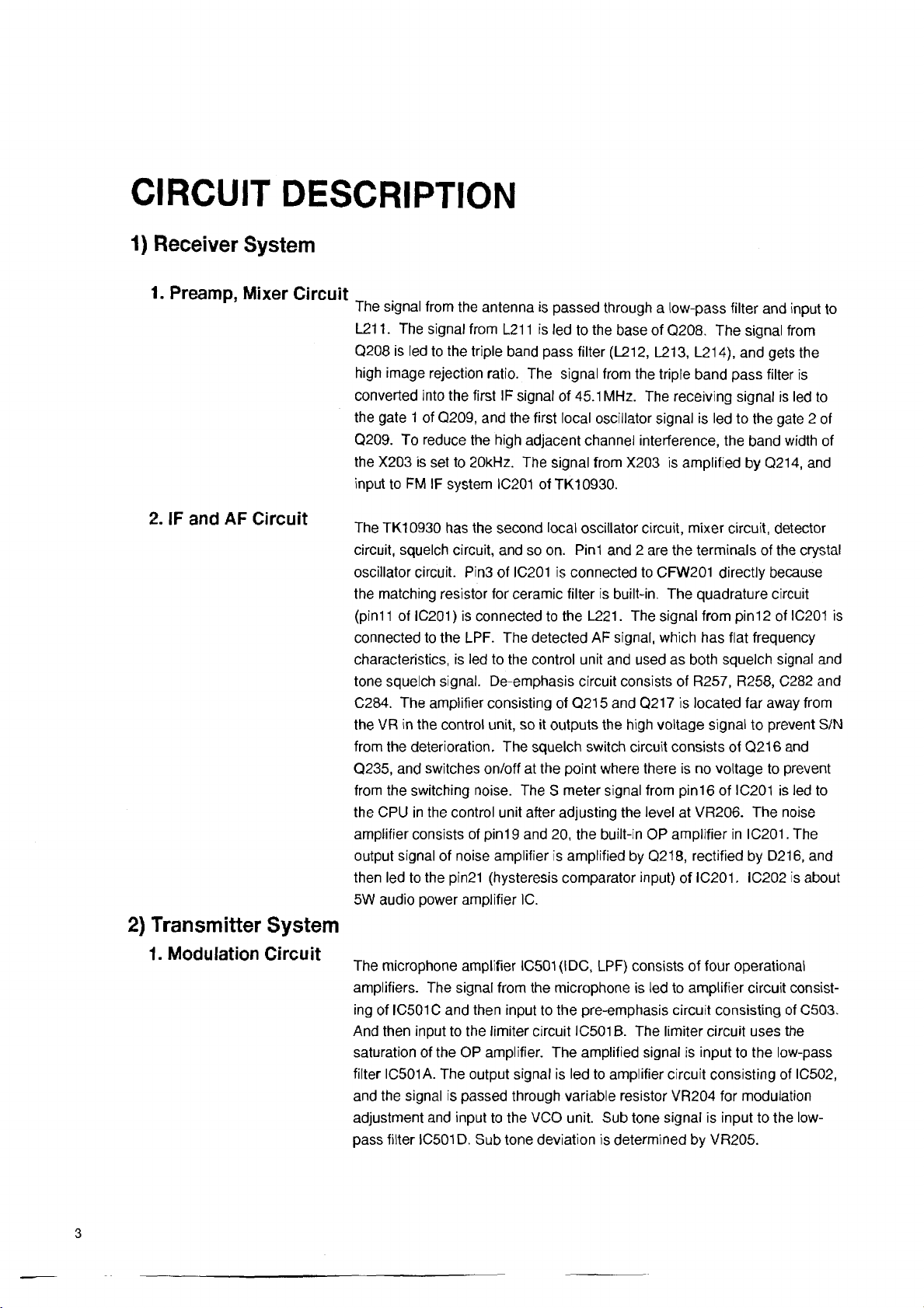
SPECIFICATIONS
1) General
Frequency Coverage:
Modulation:
Antenna Impedance:
Supply Voltage:
Current Consumption:
Frequency Stability:
Dimensions:
Weight:
Microphone:
(DR-150T)
(DR-150E)
F2, F3 (FM)
50£2 unbalanced
13.8 V DC
Transmit (High)10.0A / Receive 0.6A
+/-I0ppm max.
140mm(W) x 40mm(H) x 129mm(D)
approx. 800g (body only)
(DR-150T) EMS-12 (DTMF mic.)
(DR-150E) EMS-5A (plain mic.)
TX: 1 44 .0 00 - 147.995MHz (FM)
RX: 1 08.000- 173.995MHz (FM/AM)
RX: 440.000 ~ 449.995MHz (FM/AM)
TX: 144.0 00- 145.995MHz (FM)
RX: 144.000- 145.995MHz (FM)
RX: 430.000 - 439.995MHz (FM)
2) Transmitter
Output Power (approx.):
Modulation System:
Spurious Emission:
Max. Deviation:
Distortion at 60% modulation:
Microphone Impedance:
High 50W / Mid 25W / Low 10W
Reactance Modulation
not more than -60dB
+/ -5kHz
not more than 3%
2.2kQ
3) Receiver
Receiving System:
Intermediate Frequency:
Sensitivity (12dB SINAD):
Selectivity:
Squelch Sensitivity:
AF Output:
AF Output Impedance:
Specifications are subject to change without notice or obligation.
Specifications guaranteed in the amateur band only.
Operating temperature -10°C~+60°C
Double Conversion Superheterodyne
First: 45.1MHz / Second: 455kHz
2m band: -16dBn or better, 70cm band: -10dBji or better
-6dB: 12kHz or more, -60dB: 28kHz or less
-20dB(i or better
1.5W
8Q
Page 3
CIRCUIT DESCRIPTION
1) Receiver System
1. Preamp, Mixer Circuit
2. IF and AF Circuit
The signal from the antenna is passed through a low-pass filter and input to
L211. The signal from L211 is led to the base of Q208. The signal from
Q208 is led to the triple band pass filter (L212, L213, L214), and gets the
high image rejection ratio. The signal from the triple band pass filter is
converted into the first IF signal of 45.1 MHz. The receiving signal is led to
the gate 1 of Q209, and the first local oscillator signal is led to the gate 2 of
Q209. To reduce the high adjacent channel interference, the band width of
the X203 is set to 20kHz. The signal from X203 is amplified by Q214, and
input to FM IF system IC201 ofTK10930.
The TK10930 has the second local oscillator circuit, mixer circuit, detector
circuit, squelch circuit, and so on. Pin1 and 2 are the terminals of the crystal
oscillator circuit. Pin3 of IC201 is connected to CFW201 directly because
the matching resistor for ceramic filter is built-in. The quadrature circuit
(pinl 1 of IC201) is connected to the L221. The signal from pin12 of IC201 is
connected to the LPF. The detected AF signal, which has flat frequency
characteristics, is led to the control unit and used as both squelch signal and
tone squelch signal. De-emphasis circuit consists of R257, R258, C282 and
C284. The amplifier consisting of Q215 and Q217 is located far away from
the VR in the control unit, so it outputs the high voltage signal to prevent S/N
from the deterioration. The squelch switch circuit consists of Q216 and
Q235, and switches on/off at the point where there is no voltage to prevent
from the switching noise. The S meter signal from pin16 of IC201 is led to
the CPU in the control unit after adjusting the level at VR206. The noise
amplifier consists of p inl 9 and 20, the built-in OP amplifier in IC201. The
output signal of noise amplifier is amplified by Q218, rectified by D216, and
then led to the pin21 (hysteresis comparator input) of IC201. IC202 is about
5W audio power amplifier IC.
2) Transmitter System
1. Modulation Circuit
The microphone amplifier IC501(IDC, LPF) consists of four operational
amplifiers. The signal from the microphone is led to amplifier circuit consist
ing of IC501C and then input to the pre-emphasis circuit consisting of C503.
And then input to the limiter circuit IC501B. The limiter circuit uses the
saturation of the OP amplifier. The amplified signal is input to the low-pass
filter IC501A. The output signal is led to amplifier circuit consisting of IC502,
and the signal is passed through variable resistor VR204 for modulation
adjustment and input to the VCO unit. Sub tone signal is input to the low-
pass filter IC501D. Sub tone deviation is determined by VR205.
Page 4
2. TX Amp. Circuit
The signal from VCO is amplified by TX, RX wide band LO amplifier
Q207. The signal from Q207 is passed through the transmission/reception
selector, and amplified by Q206 and Q202. The PA unit is driven at
200mW driving power.
3. PA Circuit
4. ALC Circuit
3) PLL Circuit
IC208 is 50W powered amplifier module. The output power is controlled
by the voltage of Pin3. The RF signal amplified 50W in PA is passed
through D201 and low-pass filter, and input to the antenna connector.
The power detection circuit consisting of D204 rectifies the output signal
voltage. VR201 is middle power adjust trimmer pot. VR202ishigh
power adjust trimmer pot. The detected DC voltage is amplified by Q203,
Q204 and Q205. Output power is controlled by voltage of Pin3 in IC5 and
collector voltage of Q202. When the temperature goes up unusually, the
power down circuit consisting of Q238, R316 and TH202 works to prevent
the device from the destruction.
The VHF-VCO circuit consisting of Q402, Q404, D404, D405, and D406.
The transmission/reception shift circuit consisting of Q404. The UHF-
VCO circuit consisting of Q 401, D401, D402, and D403.
IC205 is pulse swallow system based PLL IC with the built-in prescaler,
which synthesizes 145MHz-band and 435MHz signal.
The loop filter consisting of R242, R243, R319, R320, C258, C350 and
C352.
Page 5
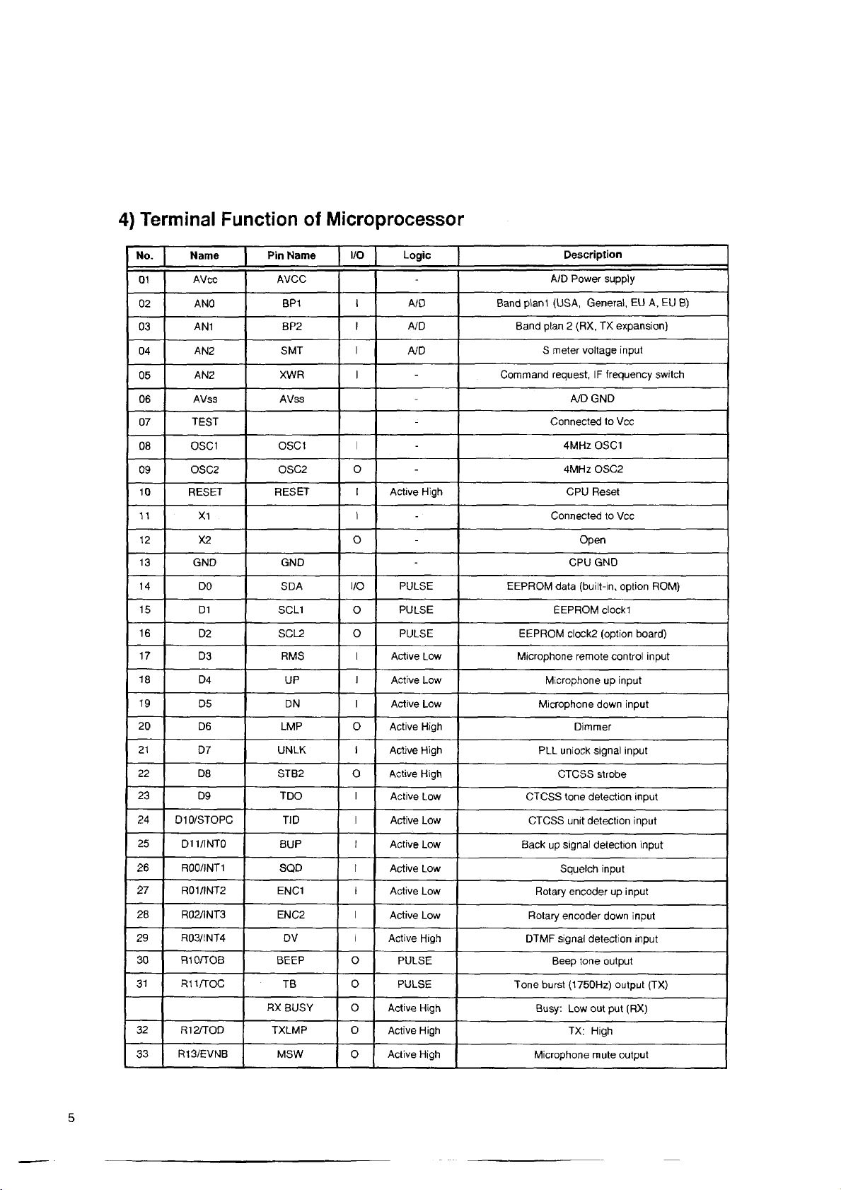
4) Terminal Function of Microprocessor
No.
01
02
03 AN1
04 AN2
05
06
07
08
09
10
11
12 X2 o
13
14 DO SDA I/O
15 D1
16
17
18
19 D5 DN I
20 D6
21 D7 UNLK
22
23
24 DIO/STOPC
25
26 R00/INT1
27
28 R02/INT3
29 R03/INT4 DV
30
31
32
33
Name
AVcc
ANQ BP1
AN2 XWR
AVss AVss
TEST
OSC1
OSC2
RESET RESET I
X1
GND GND
D2
D3 RMS
D4 UP
D8
D9
D11/INT0 BUP
R01/INT2
RIO/TOB
R11/TOC
R12/TOD TXLMP 0
R13/EVNB
Pin Name
AVCC
BP2
SMT
OSC1
OSC2 O
SCL1 o
SCL2
LMP 0 Active High
STB2
TDO
TID
SQD I
ENC1
ENC2
BEEP o
TB 0
RX BUSY o
MSW 0 Active High
I/O Logic
-
I
I
I
I
I
o PULSE
I
I
I
A/D
A/D
A/D
-
-
-
-
-
Active High
-
-
-
PULSE
PULSE
Active Low Microphone remote control input
Active Low
Active Low Microphone down input
Active High
o Active High
I
Active Low
I
Active Low
I
Active Low Back up signal detection Input
Active Low
I
Active Low
I
Active Low
I
Active High
PULSE Beep tone output
PULSE
Active High
Active High
| Description
A/D Power supply
Band planl (USA, General, EU A, EU B)
Band plan 2 (RX, TX expansion)
S meter voltage input
Command request, IF frequency switch
A/D GND
Connected to Vcc
4MHz OSC1
4MHz OSC2
CPU Reset
Connected to Vcc
CPU GND
EEPROM data (built-in, option ROM)
EEPROM clockl
EEPROM clock2 (option board)
Microphone up input
Dimmer
PLL unlock signal input
CTCSS strobe
CTCSS tone detection input
CTCSS unit detection Input
Squelch Input
Rotary encoder up input
Rotary encoder down input
DTMF signal detection input
Tone burst (1750Hz) output (TX)
Busy: Low out put (RX)
TX: High
Microphone mute output
Open
Page 6
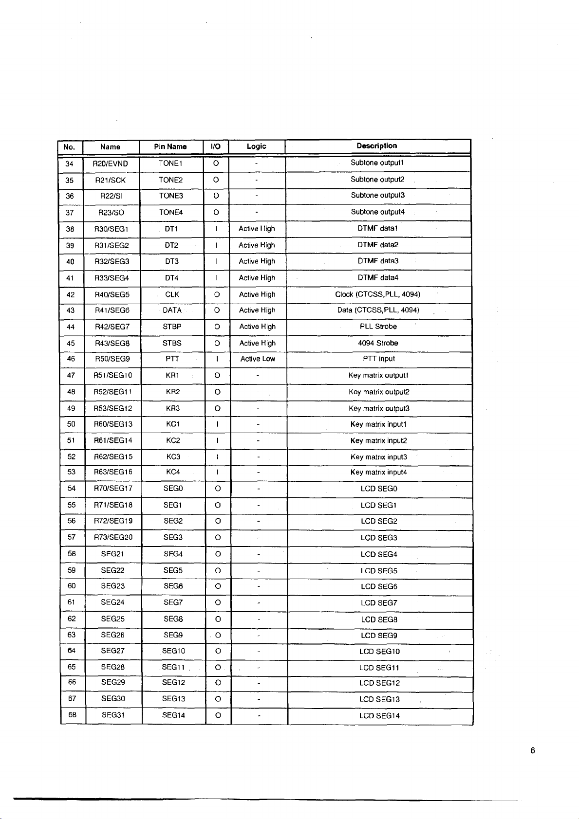
No.
34 R20/EVND
35
36 R22/SI
37 R23/SO
38 R30/SEG1
39
40
41 R33/SEG4 DT4
42 R4 0/S EG 5
43 R41/SEG6 DATA 0
44 R42/SEG7
45
46
47
48 R52/SEG11
49 R53/SEG12 KR3
50 R60/SEG13
51
52
53
54 R70/SEG17 SEGO
55 R71/SEG18
56
57
58
59 SEG22
60
61
62
63
64
65 SEG28
66 SEG29
67
68
Name
R21/SCK
R31/SEG2
R32/SEG3
R43/SEG8
R50/SEG9
R51/SEG10 KR1 o
R61/SEG14
R62/SEG15
R63/SEG16
R72/SEG19
R73/SEG20
SEG21
SEG23
SEG24
SEG25
SEG26 SEG9
SEG27 SEG10 o
SEG30
SEG31
Pin Name
TONE1 0
TONE2 0
TONE3 0 -
TONE4
DT1
DT2 I
DT3
CLK O Active High
ST BP o
STBS 0
PTT
KR2
KC1
KC2 I
KC3
KC4 I
SEG1
SEG2
SEG3
SEG4
SEG5
SEG6
SEG7 0
SEG8 0
SEG11 .
SEG12
SEG13 o
SEG14 0
I/O
0 -
Logic
-
-
I Active High
Active High
I Active High
Description
Subtone output 1
Subtone output2
Subtone output3
Subtone output4
DTMF datal
DTMF data2
DTMF data3
I Active High DTMF data4
Clock (CTCSS,PLL, 4094)
Active High
Activa High PLL Strobe
Active High 4094 Strobe
Active Low PTT input
I
-
0
0
I
I
0
0
0
0
o
0
o
o
o
o
-
-
-
-
-
-
-
-
-
-
-
-
- LCD SEG6
-
- LCD SEG8
-
-
-
-
-
-
Data (CTCSS,PLL, 4094)
Key matrix outputl
Key matrix output2
Key matrix output3
Key matrix inputl
Key matrix input2
Key matrix input3
Key matrix input4
LCD SEG0
LCD SEG1
LCD SEG2
LCD SEG3
LCD SEG4
LCD SEG5
LCD SEG7
LCD SEG9
LCD SEG10
LCD SEG11
LCDSEG12
LCD SEG13
LCD SEG14
Page 7
NO. Name Pin Name
I/O Logic Description
69
70 SEG33
71
72
73 SEG36 SEG19 O
74 SEG37
75 SEG38 SEG21
76
77 SEG40 SEG23
78
79
80
81 SEG44
82 SEG45 SEG28 - O
83 SEG46 SEG29
84
85
86
87 SEG50
88
89
90 COM1 COM1
91 COM2
92 COM3
93
94
95 V2
96
97
98 TON EC
99
100
SEG32
SEG34 ■ SEG17 0
SEG35
SEG39
SEG41 . SEG24 O
SEG42 SEG25 O
SEG43
SEG47
SEG48 SEG31 0
SEG49
SEG51
SEG52
COM4
V1 LV1
V3 LV3
Vcc VCC
TONER
VTref
SEG15 0
SEG16 0
SEG18
SEG20 O
SEG22 O
SEG26 O
SEG27 O
SEG30 O
SEG32
, SEG33 0
SEG34
SEG35
COM2 0
COM3 0
LV2
DTC
DTR O
; VTR
-
-
-
0
-
-
-
O
-
-
O
-
-
-
LCD SEG15
LCD SEG16
LCD SEG17
LCD SEG18
LCD SEG19
LCD SEG20
LCD SEG21
LCD SEG22
LCD SEG23
LCD SEG24
LCD SEG25
- LCD SEG26
-
-
O
o
0
o
0
o
-
-
-
-
-
-
-
- ;
-
-
-
-
-
-
-
0
- DTMF tone C output
-
I
-
DTMF output reference level power supply
LCD SEG27
LCD SEG28
LCD SEG29
LCD SEG30
LCD SEG31
LCD SEG32
LCD SEG33
LCD SEG34
LCD SEG35
LCD SEG36
LCD SEG37
LCD SEG38
LCD SEG39
LCD Power supply
LCD Power supply
LCD Power supply
CPU Power supply
DTMF tone R output
Page 8
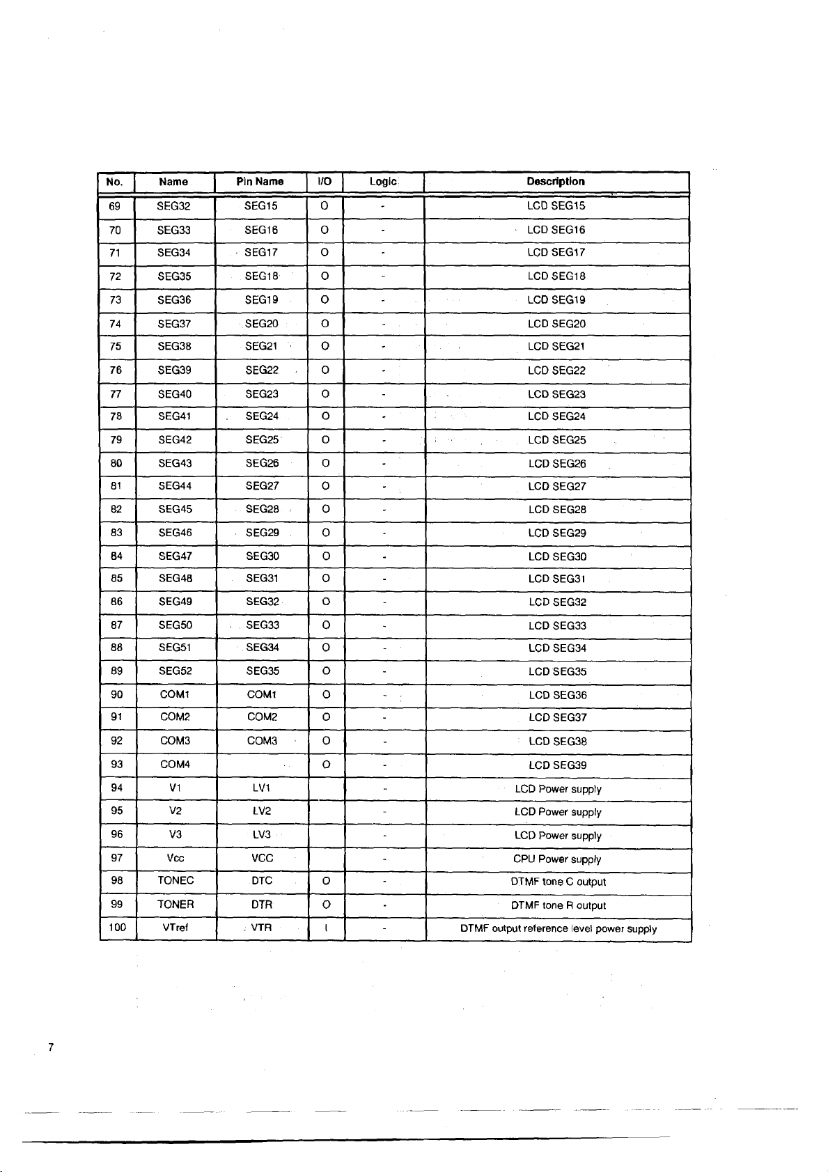
5) Terminal Function of 4094
No.
Pin Name
P1-1
P1-2
P1-3
P1-4
P1-5
PI-6
PI-7
PI-8 SIFT
RFM
RFL
- - -
R145 RX 145 power control 0
R360
R440 RX 440 power control o
R870 RX 870 power control 0
Function
RF power mid control 0
RF power low control o
RX 360 power control 0 Active Low
RX SIFT control
I/O Logic Description
Active Low L=Power Mid
Active Low L=Power Low
-
Active Low L=RX 145 power ON
L=RX 360 power ON
Active Low
Active Low
0 Active Low
L=RX 440 power ON
L=RX 870 power ON
-
L=SHIFT ON
P2-1
P2-2
P2-3
P2-4
P2-5 VCOI VCOI power control 0
P2-6
P2-7 RFATT
P2-8
-
AFMUTE
AM/FM AM/FM control o
LIZH LIZH control o
VC02 VC02 power control o
- - -
- -
AF mate control o Active High
RFATT control 0
-
Active Low L=AM
Active High
Active Low L=VC01 power ON
Active Low L=VC02 power ON
Active Low L=RF ATT ON
- -
-
H=AF mute ON
H=LIZH ON
Page 9
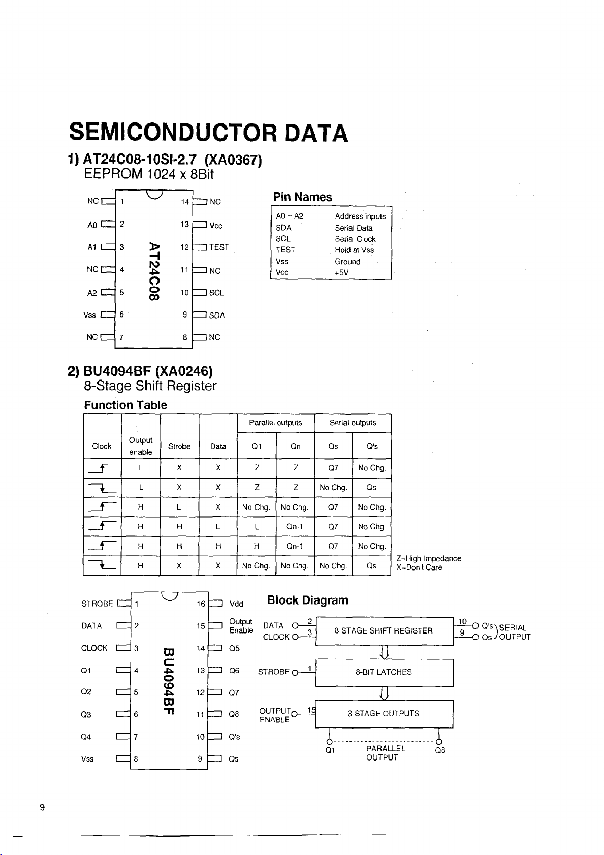
S E M I C O N D U C T O R D A T A
1) AT24C08-10SI-2.7 (XA0367)
E E P R O M 1 0 2 4 x 8 B i t
NCI
----
AO CZ
A1 CZ
NCIZZ
A2 CH
Vss CZ
NCI—
1
2
AT24C08
3
4
5
6 ■
7 8
14 ZDN C
13
— 1 Vcc
12 ZD TEST
11
IZ lN C
10 ZZISCL
9
=IS D A
ZZ1NC
2) BU4094BF (XA0246)
8 - S t a g e S h i f t R e g i s t e r
Function Table
Clock
_ r~
—L -
_ r ~
Output
enable
Strobe
L X X 2 2 Q7
L
H
X
L
Data
X
X
Pin Names
AO-A2
SDA
SCL
TEST
Vss
Vcc
Parallel outputs
Q1
Z Z
No Chg.
Serial outputs
Qn Qs
No Chg. Qs
No Chg. Q7
Address inputs
Serial Data
Serial Clock
Hold at Vss
Ground
+5V
Q's
No Chg.
No Chg.
_ r ~
^—
H H L
H
H
H H H Qn-1 Q7 No Chg.
X
L
X No Chg. No Chg. No Chg. Qs
Vdd
Output
Enable
Qn-1 Q7 No Chg.
Block Diagram
Q1 PARALLEL qs
OUTPUT
Z=High Impedance
X= Don't Care
SERIAL
OUTPUT
Page 10
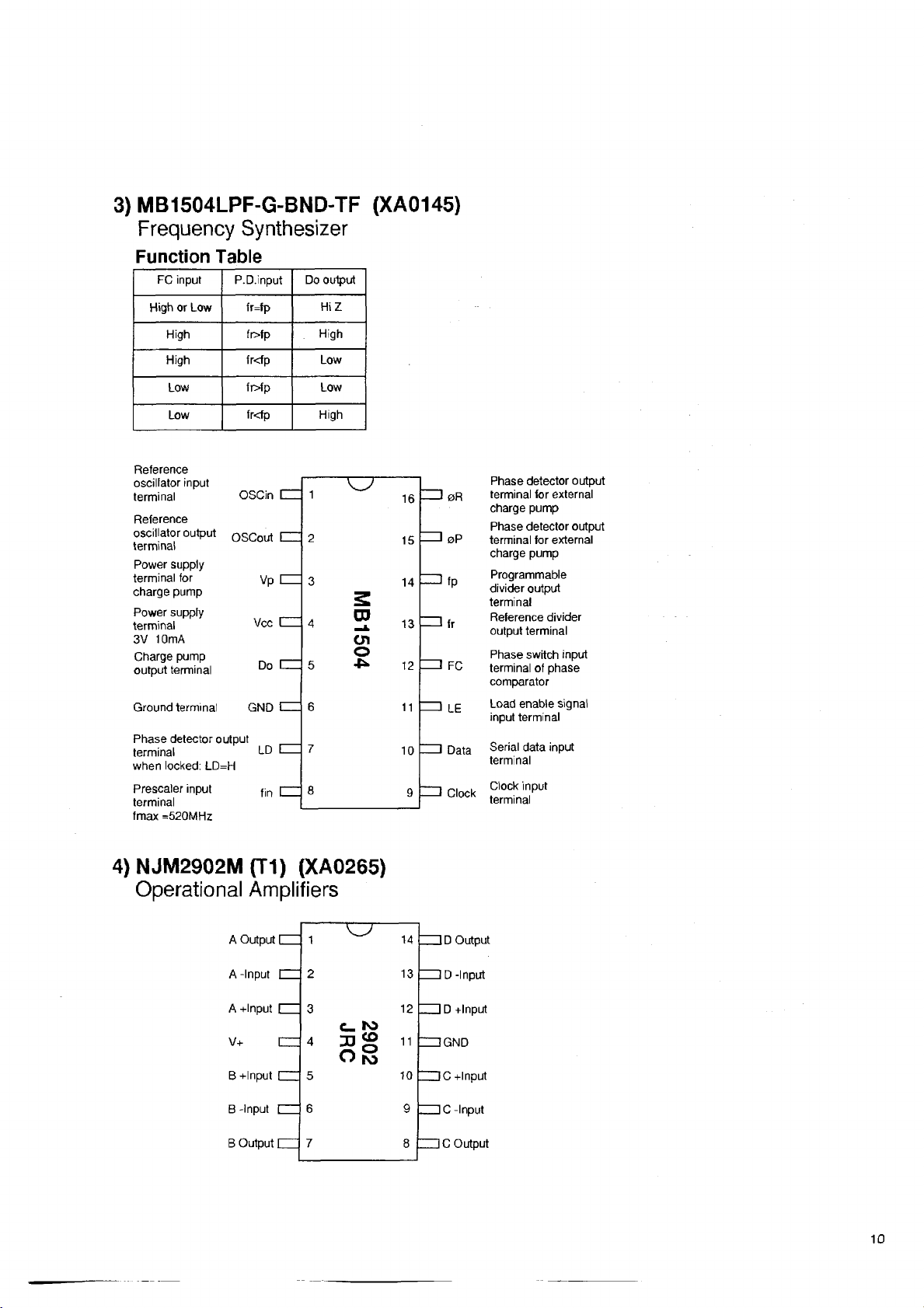
3) MB1504LPF-G-BND-TF (XA0145)
F r e q u e n c y S y n t h e s i z e r
Function Table
FC input
High or Low
High fr>fp . High
High
Low fr>fp Low
P.D.input
fr=fp
fr<fp
Do oulput
HiZ
Low
Low
Reference
oscillator input
terminal
Reference
oscillator output
terminal
Power supply
terminal for
charge pump
Power supply
terminal
3V 10mA
Charge pump
output terminal
Ground terminal
Phase detector output
terminal LD 1—
when locked: LD=H
Prescaler input
terminal
fmax =520MHz
fr<fp High
OSCin IZZ
OSCout 1
Vp IZZ
Vcc CZ
Do 1 .
GND IZZ
fin IZZ
1
2
3
2
4
5
6
7
8
03
Ü1
©
ZZ1 0R
16
= 1 0P
15
14
= l fp
= lf r
13
Z=I FC
12
11
= 1 LE
— 1 Data
10
ZZ1 Clock
9
Phase detector output
terminal for external
charge pump
Phase detector output
terminal for external
charge pump
Programmable
divider output
terminal
Reference divider
output terminal
Phase switch input
terminal of phase
comparator
Load enable signal
input terminal
terminal
Clock input
terminal
4) NJM2902M (T1) (XA0265)
O p e r a t i o n a l A m p l i f i e r s
A Output 1 14 l D Output
A -Input
A +lnput EZ
V+
B +lnput IZZ 5 10__1C +lnput
B -Input
B Output IZZ
2
t=Z
3
C _ I O
4
c z
O IO
6 9
d
7
13
i D -Input
12 ID +lnput
11
IZIGND
1 1C -Input
8 1C Output
10
Page 11
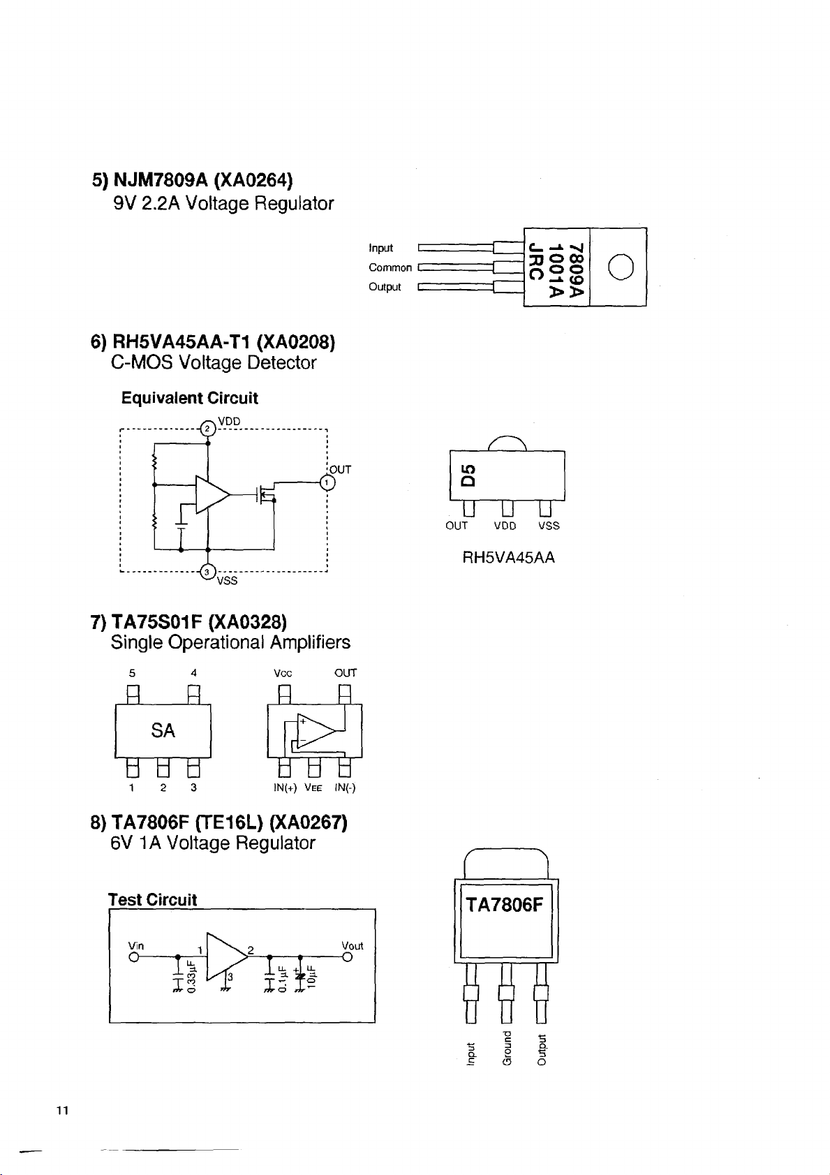
5) NJM7809A (XA0264)
9 V 2 .2A Voltage Regulator
6) RH5VA45AA-T1 (XA0208)
C - M O S V o l t a g e D e t e c t o r
Equivalent Circuit
,VDD
" 0
o
HR
vss
7) TA75S01F (XA0328)
S i n g l e O p e r a t i o n a l A m p l i f i e r s
J3UT
Input
Common C
Output C
c
1
A
in
Q
LI U U
OUT VDD VSS
RH5VA45AA
c_ -*■ -g
30»
o2 §
> >
0
" ö B ~ t J b b) ü
8) TA7806F (TE16L) (XA0267)
6 V 1 A V o l t a g e R e g u l a t o r
Test Circuit
11
IN(+) Vee IN(-)
Page 12
Output Power (W)
Input Power (W) Vcon (V)
Efficiency y {%)
Outpul Power (W}
Efficiency ? (%}
Po , 7 - Vcon
Page 13
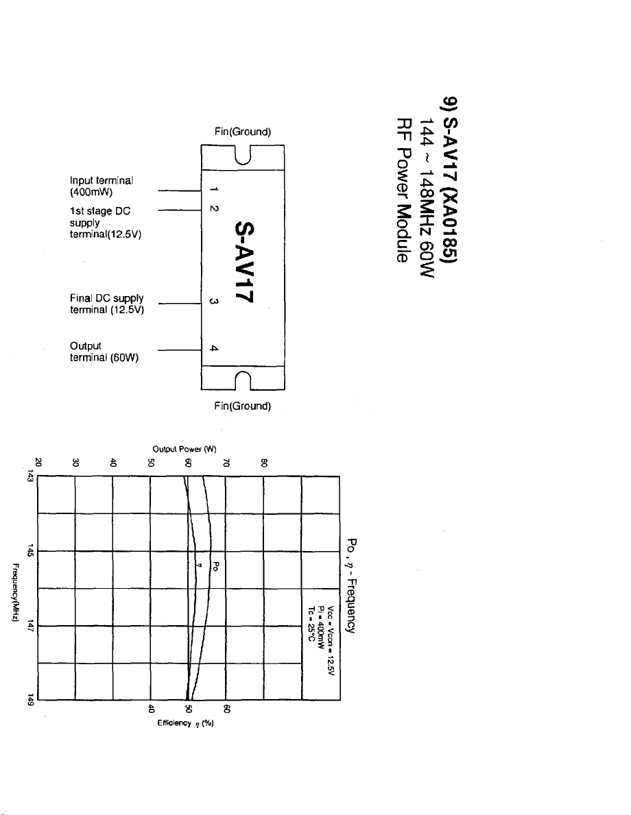
Oulpul Power (W)
S 8 3
i— m
Fin(Ground)
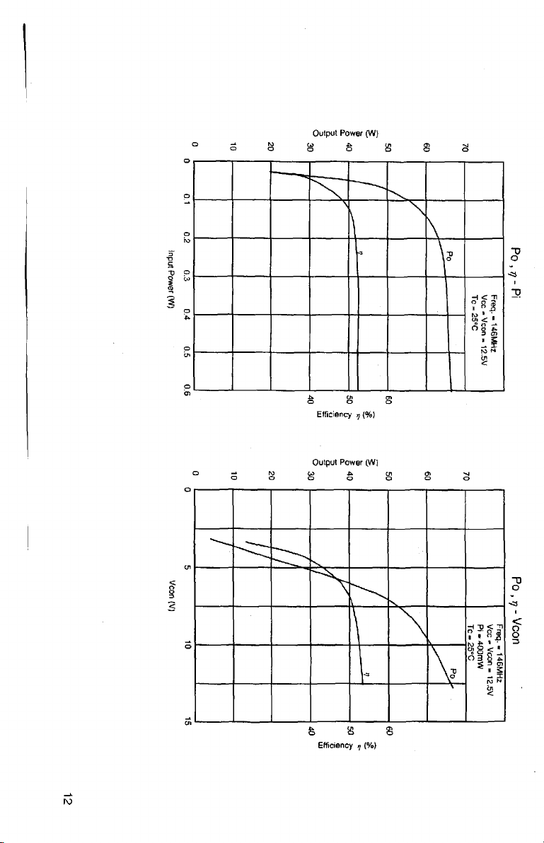
9) S-AV17 (XA0185)
1 4 4 - 1 4 8 M H z 6 0 W
RF P o w e r M o d u l e
145 1 4 7
T3
O
H TJ <
0 — 0
1 ■
0
» § <
0Î0
*1
ro
s
è S S
Efficiency 7 (%)
Page 14
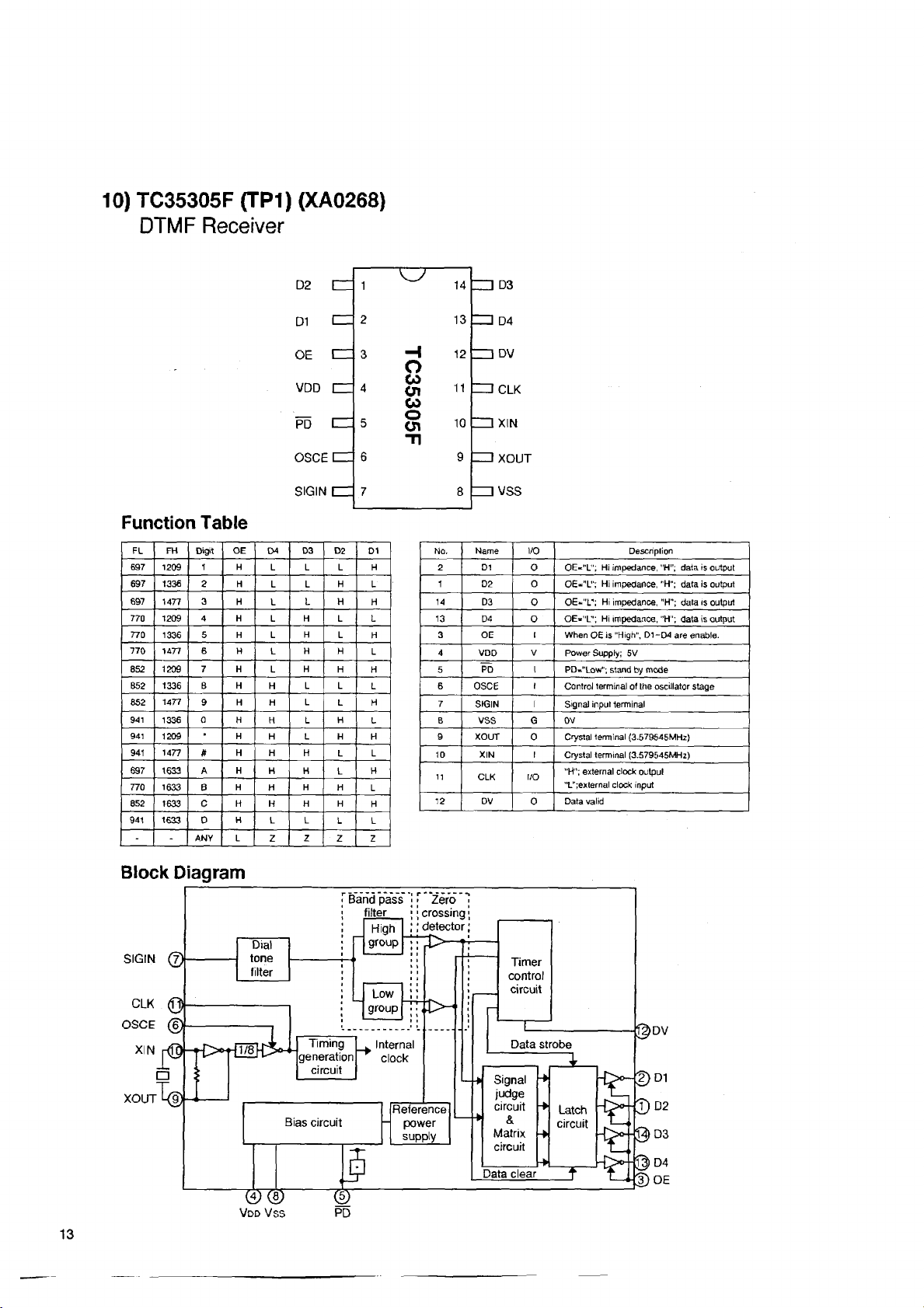
10) TC35305F (TPI) (XA0268)
D T M F R e c e i v e r
Function Table
FH
FL
697
1209
697 1336
697
1477
770 1209 4
77D
1336
1477 6 H
770
852
1209
B52 1336
1477
852
941
1336 a H
941
1209
941 1477
697 1633 A
770
1633
852
1633 C
941
1633
- -
OE
Digit
1 H
2 H
3
5 H L
7 H
e
9 H H
#
0 H
H H H H
H
D
ANY L
D2
D1
OE in
VDD
PD
OSCE
SIGIN C Z
D4
L L L H
L L
H
L
H
L H L L
L
L
H
H
H L
H
H L H
H H H
H
H H
H
L L L L
Z
D3
L H
H
H H
H
L L
L
H
Z
1
CZ
2
CZ
3
4
n z
5
r z
6
7 8
D2 D1
H
L
H
L
H
L
H
H
L
L H
H
L
H
L L
H
L
H
L
H
Z Z
w
H 12
O
CO
Of
CO
o
cn
14 — I D3
13
= □ D4
----
1 DV
11
ZU CLK
10
zu xiN
"n
9
ZZI XOUT
ZZI VSS
No. Name
2 Di
14
13 D4
3 OE 1 When OE is "High", D1-D4 are enable.
4
VDD
5 PD
6
OSCE
7
SIGIN
B
VSS G
9 XOUT
10 XIN 1
11
CLK I/O
12 DV
D2 0
D3
I/O
O 0E«"L”; Hi impedance, "H"; data is output
OE-"L'‘; Hi impedance, "H"; data is output
0 OE«'V; Hi impedance, "H“; data is output
OE*"L"; Hi impedance, ”H"; data is output
0
V
Power Supply; 5V
I
PD«"Low"; stand by mode
1
ControJ terminal of Ihe oscillator stage
[
Signal input terminal
OV
0 Crystal terminal (3.579545MH2)
Crystal terminal (3.579545MHz)
”H"; external clock outpul
”L";exlernal clock input
0 Data valid
Description
13
Block Diagram
SIGIN © -
CLK @
OSCE (6)
XIN
XOUT
■T<D
Dial
lone
filter
w
Vdd V ss
Timing
generation
circuit
Bias circuit
-W
PD
Timer
control
circuit
g>DV
Internal
Data strobe
clock
-»
Signal
judge
-►
Reference
-
power
supply
$
circuit
&
Matrix
circuit
Data clear
Latch
circuit
>
s
i::
|) D 1
2 ) 0 2
Q>qz
3>D4
D o e
Page 15

11) TK10930VTL (XA0223)
Characteristic Symbol Min.
Supply Current 1
Supply Current 2
Mixer Conversion Gain
Mixer Input Impedance
FM
Limiting Sensitivity Limit
Output Voltage
Distortion
Output Impedance
Filter Gain
Scan Control Hi Voltage
Scan Control Low Voltage
Squelch Hysteresis Hys
S meter Output Voltage
S meter Output Voltage S1
S meter Output Voltage
S meter Output Voltage
S meter Output Voltage
S meter Output Voltage
AM
Sensitivity
Output Voltage
Distortion-1 THD2
Distortion-2
S/N
AM OFF
Icc1
Icc2
Mg 20 dB
Mz
Vo1
THD1
Zo 800
Gf
SH
SL
SO
S2 0.7
S3 1.2 1.8
S4 1.6 2.3 2.9
S5
US 20
Vo2 60 120
THD3
Vo1
Vo
Typical
6.8 8.9 mA No signal, AM ON
3.9 5.3 mA No signal, AM OFF
3.6
2.0 8.0
85
30
2.3
0.05 0.5
1.8
40 48
-0.3 0.3
150
1.0
38
30
0.05
1.2 1.7 V Vin=0.1mV, RS=68k£2
2.4
15
1.0 2.0
2.0
Max Typical Condition
230 mVrms
0.3
0.5
0.9 V
2.5 V
2.9
160 mVrms 1kHz, 30%, Vin=1mV
4.0
2.0
Kß DC Test
-3.0dB
MV
10mVin+/-3kHz DEV
% lOmVin +/-3kHz DEV
10mVin
£2
dB Fin=30kHz, Vo=l00mV
V Squelch input=2.5V
V
Squelch input-OV
mV
V Vin=0mV, RS=68kfl
Vin=0.01mV, RS=68ki2
Vin=1mV, RS=68kQ
V Vin=10mV, RS=68k£2
V Vin=100mV, RS=68ki2
fiV When output is 20mVrms.
1kHz, 30%, Vin=1mV
%
% 1kHz, 30%, Vin=1mV
dB 1 kHz, 30%, Vin=1 mV
% OFF
Page 16

12) TC4W66FU (TE12L) (XA0306)
D u a l B i l a t e r a l S w i t c h
IN/OUT 1 n z
OUT/IN 1
CONT2 n z
VSS
13) HPC1241H (XA0079)
A u d i o P o w e r A m p l i f i e r s
r z
n z
1 •
2
3
4
£
05
o>
8 — 1 VDD
7
m CONT1
6 ZH OUT/IN 2
5
ZH IN/OUT 2
15
Page 17

14) Transistor, Diode and LED Outline Drawings
Top View
Page 18

15) LCD Connection
(EL0025)
/ e s g l T I s S I
ts s m KL E3 D IAL BBES3 PR! E V S A M iB
SPLIT
• : . i i ii T i T i T r r i n n n n n n T T [ T n n n n n T i T T r T n n n n n m n n n n n T iT T iT n ~ ~
— o>
o
Z o
1 2 3 4 5 6 7 8
Pin No.
1 0
2
3
4 3 BUSY (1)c
5
6 5
7
8
9 8 1b.c
10 9
11
12
13
14
15
16 15 P
17
1B 17
19 18
20
Signal
Name
Pin No. 90
COM1
>
1 SKIP (2)b (2)a
2 ATT
4
M
0
6
7
10
11 RC
12
13
14 G 4c 4b
16
19
FUNC 2e
2d
KL 3e 3f 30 COM.2
3d
DIAL
4d
5d
DSQ
PRI 6e 6f 39 35
6d 6g 6a
(1) (2) (3) (4) 15) {6) (7]
Pin No. 91
COM2
(3)b
(1)b
(2)c
(3)c
2g
2c 2b
3g
3c 3b
4e
4g
5e 5f
5g
5c 5b
Pin No. 92
COM3
(3)a
(1)a
(1)d 24
(2)d
(3)d 26
2f
2a 28
3a
4f
4a
5a
Pin No.
21
22
23
25
27 26 M
29
31
32
33
34 30
35
36
37
38
Signal
Name
..........
00
z
Pin No. 90
COM1
20
21
22
23
24 AM 8e 8f
25 8d
27 L 25 50
COM.1
28
29
31
32 T
33
34
RPT (7)c
SPLIT (5)b
Pin No. 91
COM2
•
TS
7d
VS 7c 7b
75
—
+
(7)b
SQ (6)b (6)a
(4)b (4) a
Pin No. 92
COM3
6c 6b
7e 7f
7g
8g
8c 8b
(4)c
(5)c (5)d
(6)c (6)d
7a
8a
COM.3
(4)d
(7)d
(7)a
(5)a
17
Page 19

E X P L O D E D VIEW
1) Bottom View
FF0031
2) LCD View
18
Page 20

„ « o * '® ''4
C t O ' '
- { O p * f ^ o c 3 '
« tss &
Page 21

P A R T S LIST
Ref.
Parts No.
No.
CU3035 Chip C. C1608JB1H102KT-A
C101
C102 CU3059 Chip C. C1608JF1E104ZT-A
C103 CU3059 Chip C. C1608JF1E104ZT-A
C104 CU3047 Chip C. C1608JB1H103KT-A
CU3059 Chip C. C1608J F1E104ZT-A
C105
C106
CU3059
CU3047 Chip C.
C107
CU3035 Chip C. C1608JB1H102KT-A
C108
CU3035 Chip C.
C109
CU3035 Chip C. C1608JB1H102KT-A
C110
CU3035 Chip C. C1608JB1H102KT-A
c m
C112 CU3035 Chip C. C1608JB1H102KT-A
C114
CU3035 Chip C.
C115
CU3035
CU3023 Chip C.
C116
CU3035 Chip C. C1608JB1H102KT-A
C120
C121
CU3023
C122 CU3023 Chip C.
C123 CU3035 Chip C. C1608JB 1H102KT-A
C124
CU3023 Chip C.
CU3035
C125
C126 CU3035 Chip C.
C127 CU3023
C128 CU3035
C129
CU3035 Chip C.
C130
CU3035 Chip C.
CU3035
C131
C132 CU3047 Chip C.
C133 CU3047
C134
CU3035 Chip C.
C135
CU3023
C136 CU3023 Chip C.
C137
CU3035 Chip C.
C138 CU3035
C139 CS0220
C140 CU3023 Chip C.
C141
CU3059
C142 CU3023
CU3023
C145
C146 CS0220
C147 CU3023
C148
CU3059 Chip C.
CU3047
C150
C151 CU3031
C152
CS0220
C153
CU3017 Chip C.
C154 CU3017
C155 CU3059
C156
CS0220
C157
CS0220
C158
CU3059 Chip C.
Description Parts Name
CPU Unit
Chip C. C1608JF1E104ZT-A
C1608JB1H103KT-A
C1608JB1H102KT-A
C1608JB1H102KT-A
Chip C.
Chip C.
Chip C.
Chip C.
Chip C.
Chip C.
Chip C.
Chip C.
Chip C.
Chip Tantal
Chip C.
Chip C.
Chip C.
Chip Tantal TMCMA1C225MTR
Chip C.
Chip C.
Chip C.
Chip Tantal
Chip C.
Chip C.
Chip Tantal
Chip Tantal
C1608JB1H102KT-A
C1608CH1H101JT-A
C1608CH1H101 JT-A
C1608CH1H101 JT-A
C1608CH1H101 JT-A
C1608JB1H102KT-A
C1608JB1H102KT-A
C1608CH1H101JT-A
C1608JB1H102KT-A
C1608J B1H102KT-A
C1608JB1H102KT-A
C1608JB1H102KT-A
C1608JB1H103KT-A
C1608JB1H103KT-A
C1608JB1H102KT-A
C1608CH1H101 JT-A
CI6O8CHIHIO1 JT-A
C1608JB1H102KT-A
C1608JB1H102KT-A
TMCMA1C225MTR
C1608CH1H101JT-A
C1608JF1E104ZT-A
C1608CH1H101 JT-A
C1608CH1H101JT-A
C1608CH1H101 JT-A
C1608JF1E104ZT-A
C1608JB1H103KT-A
C1608JB1H471KT-A
TMCMA1C225MTR
C1608CH1H330JT-A
C1608CH1H330JT-A
C1608JF1E104ZT-A
TMCMA 1C225MTR
TMCMA 1C225MTR
C1608JF1E104ZT-A
Ref.
Ver.
IC102 XA0268 IC
J101
J102 UE0192
J103
J104 UE0194
L101
LC101 EL0025
LC102
LC103 DG0014 LCD Light
LC104 FG0141
LC105 TL0009 LCD Filter
LC106 TL0010
LD101 XL0032 LED CL-170YG-CD-T
LD102 XL0032
LD103 XL0032
LD104
LD105
LD106 XL0032 LED CL-170YG-CD-T
LD107 XL0032 LED
LD108 XL0032 LED
LD109 XL0038
LD110 XL0038
LD111
LD112
LD113
. LD114 XL0038
LD115 XL0032 LED CL-170YG-CD-T
LD116
LD117
LD118 XL0032
LJ101
LJ103
LS101 UQ0014
M1101
Parts No.
No.
XD0187 Diode
D101
D102
XD0231
D103
XD0231
D106
XD0231
XD0230 Diode
D108
D109 XD0230
IC101 XA0371 IC
IC103 XA0208
IC104 XA0328
IC105 XA0306
UE0192
UE0170
QC0334 Coil
FM0086
XL0032
XL0032
XL0038
XL0038
XL0038
XL0032
XL0032 LED CL-170YG-CD-T
MRCLH8GG Lead #30RH1-085-H1
MACLH8GG
FP0034 Mic. Spacer
Description Parts Name
Diode
Diode
Diode
Diode
IC RH5VA45AA-T1
IC
IC
Connector
Connector
Connector
Connector
LCD HLC8413-012301
LED
LED
LED CL-170YG-CD-T
LED CL-170YG-CD-T
LED
LED
LED
LED
LED
LED
LED
LED
Lead
_#30AH 1 -085-H1
CPU Unit
Ver.
DTZ11 B{TT11)
DAP202U(T106)
DAP202U{T106)
DAP202U(T106)
DAN202U(T106)
DAN202U(T106)
HD404629H_T/E
TC35305F(TP1)
AT24C08-10SI-2.7
TC4W66FU{TE12L)
11R-JE
11R-JE
B9B-ZR
FM214-8SMPYNW
N L453232T-271J
LCD Holder
LCD Connector
LCD Filter
CL-170YG-CD-T
CL-170YG-CD-T
CL-170YG-CD-T
CL-170YG-CD-T
CL-200YG-C-TS
CL-200YG-C-TS
CL-200YG-C-TS
CL-200YG-C-TS
CL-200YG-C-TS
CL-200YG-C-TS
CL-170YG-CD-T
CL-170YG-CD-T
LS22BB-2SD/PG-T
PC101
UP0258A
P.C.B
Page 22

Ref.
Parts No. Description
No.
Q101
XT0113
XU0029
Q102
Q103 XU0088 Transistor
Q104
XU0042 Transistor
Q105
XU0112 Transistor
Q106
XU0029
Q107
XU0152 Transistor
Q108
XU0029
Q109 XU0029 Transistor
Q110
XU0157 Transistor
Q112
XU0029
Q113
XU0029
R101
RK1020
R102 RK3001
RK3074 Chip. R
R103
R104 RK3074 Chip. R ERJ3GSYJ105V
RK3041 Chip. R
R105
RK3028
R106
R107
RK3028
R108 RK3038
R109 RK3036
R110 RK3062
R111 RK3062
R112
RK3065
R113 RK3038
R114
RK3058
R115 RK3062
R116 RK3001
R117 RA0020 Chip. R EXBV8V473JV
R118 RK3058
R119 RK3058
RK3057
R120
R121
RK3045
RK3054 Chip. R ERJ3GSYJ223V
R122
RK3046 Chip. R ERJ3GSYJ472V
R123
R124 RK3058 Chip. R
R125 RA0008
RA0008
R126
R127
RA0009
R128 RA0008
R129 RK3038 Chip. R
R130 RK1020
RK3050 Chip. R ERJ3GSYJ103V
R131
R132 RK4051 Chip. R
R133
RK3001
R134 RA0019
R A0008
R135
R136
RK3001
R137
RK3058
R138 RK3070
RK3060
R139
RK3061
R140
RK3057 Chip. R
R141
T ransistor
T ransistor
Transistor
T ransistor
Transistor
Transistor
Chip. R
Chip. R
Chip. R
Chip. R
Chip. R ERJ3GSYJ102V
Chip. R
Chip. R
Chip. R
Chip. R ERJ3GSYJ184V
Chip. R ERJ3GSYJ102V
Chip. R
Chip. R
Chip. R
Chip. R ERJ3GSYJ473V
Chip. R ERJ3GSYJ473V
Chip. R
Chip. R
Chip. R EXBV4V102JV
Chip. R EXBV4V102JV
Chip. R EXBV8V102JV
Chip. R
Chip. R
Chip. R ERJ3GSY0R00V T
Chip. R EXBV4V473JV
Chip. R EXBV4V102JV
Chip. R
Chip. R ERJ3GSYJ473V
Chip. R
Chip. R ERJ3GSYJ683V
Chip. R
Parts Name
2SC2873YTE12L
DTC114YUT106
2SA1213Y(TE12L)
FMC1 (T98)
DTA114YUT106
DTC114YUT106
UMC5(TR)
DTC114YUT106
DTC114YUT106
UMD3(TR)
DTC114YUT105
DTC114YUT106
ERJ8GEYJ151V
ERJ3GSYOROOV
ERJ3GSYJ105V
ERJ3GSYJ182V
ERJ3GSYJ151V
ERJ3GSYJ151V
ERJ3GSYJ681V
ERJ3GSYJ104V
ERJ3GSYJ104V E
ERJ3GSYJ473V
ERJ3GSYJ104V
ERJ3GSYOROOV
ERJ3GSYJ393V
ERJ3GSYJ392V
ERJ3GSYJ473V
EXBV4V102JV
ERJ3GSYJ102V
ERJ8GEYJ151V
ERJ14YJÏ01H
ERJ3GSYOR0OV
ERJ3GSYJ474V
ERJ3GSYJ823V
ERJ3GSYJ393V
Ref.
Ver.
R155
R156
R157 RK1106
R160 RK3058
R161
R162
R173
R174
R175
S101 UR0002 Switch
S102
S103
S104 UU0015 Switch
S105
S106
S107 UU0015 Switch SKQD-901
S108
S109
S110
S111 UQ0011
VR101
VR102 RV0021 Trim. Pot RK09K1130-10KB
X101
X102
Parts No.
No.
RK3050 Chip. R
R142
R143 RK3040
R144
RK4063
RK1020 Chip. R
R145
RK3054
R146
R147 RK3050
RK3028
R149
RK3060
R150
RK3049
R151
R152 RK3056
R152 RK3001 Chip. R
R153 RK1020 Chip. R ERJ8GEYJ151V
R154 RA0009
RA0009
RK3010
RK3058
R159
RK3059
RK3062
RK3001
R165
RK3072
R170
RK3061
R172
RK3044 Chip. R ERJ3GSYJ332V
RK3044
RK3074
UU0015 Switch SKQD-901
UU0015 Switch
UU0015 Switch SKQD-901
UU0015
UU0015 Switch SKQD-901
UU0015 Switch
UU0015
RV0020 Trim. Pot
XB0010 Crystal
XQ0045 Crystal DSMAT3.58MHZJ8P
YZ0131 Filament Tape 12x1 mm
Description Parts Name
ERJ3GSYJ103V
Chip. R ERJ3GSYJ152V
Chip. R
Chip. R
Chip. R
Chip. R
Chip. R ERJ3GSYJ683V E
Chip. R ERJ3GSYJ822V
Chip. R
Chip. R
Chip. R
Chip. R ERJ3GSYJ4R7V
Chip. R ERJ8GEYJ3R3V
Chip. R ERJ3GSYJ473V
Chip. R
Chip. R ERJ3GSYJ563V
Chip. R
Chip. R
Chip. R
Chip. R
Chip. R
Chip. R ERJ3GSYJ105V
Switch SKQD-901
Switch
Switch ESB-64801
ERJ14YJ181H
ERJ8GEYJ151V
ERJ3GSYJ223V
ERJ3GSYJ103V
ERJ3GSYJ151V
ERJ3GSYJ333V
ERJ3GSY0R00V T
EXBV8V102JV
EXBV8V102JV
ERJ3GSYJ473V
ERJ3GSYJ104V
ERJ3GSY0R00V
ERJ3GSYJ684V
ERJ3GSYJ823V
ERJ3GSYJ332V
EVQ-WQGF1524B
SKQD-901
SKQD-901
SKQD-901
SKQD-901
RK09K1130-1 OKA
CSAC4.00MGC100-TC
CPU Unit
Ver.
E
21
Page 23

MAIN Unit
Ref.
Parts No. Description Parts Name
No.
MAIN Unit
CC0061 Chip C. CC45CH1 H330JYA_F=2.5
C201
C202 CC0Û61
CU3003
C203
CU3004 Chip C.
C204
CU 3011
C205
CC0061
C206
C207
CU3035
C208 CU3035
CU3012 Chip C. C1608CH1H120 JT-A
C210
C211 CU3035
CS0227
C212
CS0227 Chip Tantal TMCMC1D106MTR
C213
C214 CU3035
C215
CU3035
CU3088
C216
C217 CU3016
CU3035 Chip C. C1608JB1H102KT-A
C218
CU3035
C219
C221
CU3035
CU3011
C222
C223 CU8042
C224 CU3035
C225 CS0221
CU3014
C226
C227 CU3019
CU3035 Chip C.
C228
C229 CU3035
C230 CU3035 Chip C.
C231 CU3035
C232
CU3023
C233 CU3035
C234
CU3006
C235
CU3035
CU3035
C236
C237 CU3012
C238
CU3009
C239 CU3035 Chip C.
CU3035
C240
C241
CU3035 Chip C.
C242
CU3019
C243
CU3009
C244 CU3047
C245
CS0372
C246 CU3031 Chip C.
C247 CU3031 Chip C-
C248 CU3035 Chip C.
C249
CU3031 Chip C.
C250
CU3006 Chip C.
C251
CU3035
C252
CU3023 Chip C.
CU3019
C253
C254
CU3019
CS0049
C255
Chip C.
Chip C.
Chip C. C1608CH1H1OOCT-A
Chip C. CC45CH1H330J YA_F=2.5
Chip C.
Chip C.
Chip C. C1608JB1H102KT-A
Chip Tantal
Chip C.
Chip C.
Chip C.
Chip C.
Chip C.
Chip C.
Chip C.
Chip C. C2012JB1C104KT-A
Chip C.
Chip Tantal TMCMB1C475MTR
Chip C.
Chip C.
Chip C.
Chip C.
Chip C-
Chip C.
Chip C.
Chip C.
Chip C.
Chip C.
Chip C.
Chip C.
Chip C.
Chip C.
Chip C.
Chip Tantal
Chip C.
Chip C.
Chip C.
Chip Tantal
CC45CH1H330J YA_F»2.5
C1608CH1H020CT-A
C1608CH1H030CT-A
C1608JB1H102KT-A
C1608JB1H102KT-A
TMCMC1D106MTR
C1608JB1H102KT-A
C1608JB1H102KT-A
C1608CH1H200JT-A
C1608CH1H270JT-A
C1608JB1H102KT-A
C1608JB1 H102KT-A
C1608CH1H10OCT-A
C1608JB1H102KT-A
C1608CH1H180 JT-A
C1608CH1H470JT-A
C1608JB1H102KT-A
C1608JB1 H102KT-A
C1608JB1H102KT-A
C1608JB1H102KT-A
C1608CH1H101JT-A
C1608JB1H102KT-A
C1608CH1H050CT-A
C1608JB1H102KT-A
C1608JB1H102KT-A
C1608CH1H120JT-A
C1608CH1H080CT-A
C1608JB1H102KT-A
C1608JB1H102KT-A
C1608JB1H102KT-A
C1608CH1H470JT-A
C1608CH1H080CT-A
C1608JB1H103KT-A
TMCMB1C106MTR
C1608JB1H471KT-A
C1608JB1H471KT-A
C1608JB1H102KT-A
C1608JB1H471 KT-A
C1608CH1H050CT-A
C1608JB1H102KT-A
C1608CH1H101 JT-A
C1608CH1H470JT-A
C1608CH1H470JT-A
TMCSA1C105MTR
Ref.
Ver.
C269 CU3035
C270
C271
C272
C273
C274
C275
C276
C277 CU8042
C278
C279 CS0373
C280
C281 CU8042
C282
C283
C284
C285
C286
C287 CU8042
C288
C289 CU8042
C290
C291 CU3051
C292 CU3047
C293
C294 CS0063 Chip Tantal TMCSA1V104MTR
C295
C296
C297
C298 CS0372 Chip Tantal
C299 CU3051 Chip C. C1608JB1E223KT-A
C301
C302 CU3001
E
C303
C304 CU3002
E
C305 CU3031
C306
C307
C308
C309
C310
Parts No.
No.
CU3035
C256
CS0049
C257
CS0063
C258
CU3035
C259
CU3035
C260
CS0373
C261
CS0373
C262
CE0355
C263
CU3035
C264
CS0227
C265
CU3035
C266
C267 CU8042
CU3023
C268
CU3012
CU3047 Chip C.
CU3020
CU3022
CU3047 Chip C.
CU8042 Chip C.
CU8042 Chip C.
CU8042
CU8042
CU3047
CU3047 Chip C. C1608JB1H103KT-A
CU8042 Chip C. C2012 J B1C104 KT-A
CU8042
CS0049 Chip Tantal TMCSA1C105MTR
CU3047 Chip C.
CU8042
CU3047 Chip C.
CU3047 Chip C.
CU3047
CU3035
CU3047
CU3003
CU3013
CU3035
CU8042 Chip C. C2012JB1C104KT-A
CE0340
CE0351
Description
Chip C.
Chip T antal
Chip T antal
Chip C.
Chip C.
ChipTantal
ChlpTantal
Electrolytic.C
Chip C.
Chip Tantal
Chip C.
Chip C.
Chip C,
Chip C. C1608JB1H102KT-A
Chip C. C1608CH1H120JT-A
Chip C.
Chip C.
Chip C.
Chip C. C2012JB1C104 KT-A
Chip Tantal
Chip C.
Chip C.
Chip C.
Chip C. C2012JB1C104 KT-A
Chip C. C2012 JB1C104KT-A
Chip C. C2012JB1C104KT-A
Chip C.
Chip C.
Chip C. C1608JB1H103KT-A
Chip C.
Chip C.
Chip C.
Chip C.
Chip C.
Chip C.
Chip C.
Chip C.
Chip C. C1608JB1H102KT-A
Electrolytic.C
Electrolytic.C 16MV220HC
C1608JB1H102KT-A
TMCSA1C105MTR
TMCSA1V104MTR
C1608JB1H102KT-A
C1608JB1H102KT-A
TMCMD1C476MTR
TMCMD1C476MTR
25MV1000HC+T
C1608JB1H102KT -A
TMCMC1D106MTR
C1608JB1H102KT-A
C2012JB1C104KT-A
C1608CH1H101 JT-A
C1608JB1H103KT-A
C1608CH1H560JT-A
C1608CH1H820JT-A
C1608JB1H103KT-A
C2012JB1C104 KT-A
C2012JB1C104KT-A
C2012 JB1C104KT-A
TMCMD1C476MTR
C2012JB1C104KT-A
C2012JB1C104KT-A
C1608JB1H103KT-A
C1608JB1H103KT-A
C2012JB1C104KT-A
C1608JB1 E223KT-A
C1608JB1H103KT-A
C1608JB1H103KT-A
C1608JB1H103KT-A
C1608JB1H102KT-A
TMCMB1C106MTR
C1608JB1H103KT-A
C1608CH1H0R5CT-A
C1608CH1H020CT-A
C1608CH1H010CT-A
C1608JB1 H471 KT-A
C1608CH1 H150JTA
16MV47HW+TS
Parts Name
Ver.
E
E
E
E
Page 24

Ref.
Parts No.
No.
C311 CE0340
CE0192
C312
CE0355
C313
C314 CU8042
CU3035 Chip C. C1608JB1H102KT-A
C315
C317 CU9009 Chip C.
CU3014
C318
CU3003
C319
CU3035 Chip C.
C320
CU3047 Chip C. C1608JB1H103KT-A
C321
CU3017
C322
CU3035
C323
C324 CU3035
CU3035 Chip C. C1608JB1H102KT-A
C325
CU3019 Chip C.
C326
C327 CU3019
CU3019
C328
CU3035
C329
CU3047
C330
CS0049 Chip T antal
C331
C332 CU3010 Chip C.
CU3004 Chip C. C1608CH1H030CT-A
C333
CU3005 Chip C.
C334
CU3035
C335
CU3035 Chip C. C1608JB1H102KT-A
C336
CU3035 Chip C. C1608J B1H102 KT-A
C337
CU3035 Chip C. C1608JB1H102KT-A
C338
CU3035
C339
CU3003 Chip C.
C340
C341 CU3035
CU3035 Chip C. C1608J B1H102KT-A
C342
CS0372 Chip Tantal
C343
CS0237 Chip Tantal
C350
CU3035
C351
CS0232
C352
CU3035 Chip C. C1608JB1 H102KT-A E
C353
CE0351 Electrolytic.C 16MV220HC
C354
XC0016
CF201
D201
XD0295
XD0014
D202
XD0130 Diode DA204U(T106)
D203
D204 XD0130 Diode DA204U(T106)
D205 XDQ128
XD0272
D206
D207 XD0131
XD0131 Diode
D208
XD0131 Diode
D209
XD0131 Diode 1SV214( TPH4)
D210
D211 XD0272
D212 XD0272
XD0272 Diode
D213
D214
XD0272
Description
Electrolytic.C 16MV_47HW+TS
Electrolytic.C
Electrolytic.C
Chip C. C2012J B1C104KT-A
Chip C. C1608CH1H180JT -A
Chip C. C1608CH1H020CT-A
Chip C. C1608CH1H330JT-A
Chip C.
Chip C.
Chip C. C1608CH1H470JT-A
Chip C. C1608CH1H470JT-A
Chip C.
Chip C. C1608JB1H103KT-A
Chip C.
Chip C. C1608JB1H102KT-A
Chip C.
Chip C.
Chip Tantal
Filter
Diode
Diode
Diode
Diode
Diode
Diode
Diode 1SS356_TW11
Diode
Parts Name
16MV_470HW
25MV1000HC+T
C3216JB1H103KT-A
C1608JB1H102 KT-A
C1608JB1H102KT-A
C1608JB1H102KT-A
C1608CH1H470JT-A
C1608JB1H102KT-A
TMCSA1C105MTR
C1608CH1H090CT-A
C1608CH1H040CT-A
C1608JB1H102KT-A
C1608CH1H020CT-A
C1608JB1H102KT-A
TMCMB1C106MTR
TMCMA1A475MTR
C1608J B1H102KT-A
TMCMA1V474MTR
CFWS455F
UM9401-RK
MI308
MA713(TX)
1SS356_TW11
1SV214( TPH4)
1SV214( TPH4)
1SV214( TPH4)
1SS356_TW11
1SS356_TW11
1SS356 TW11
Ref.
Ver.
D219
D220 XD0014
D221
D225 XD0103
IC202
IC203
IC204
IC205
IC206
IC207
J202
J203 UE0191
J204 UE0191
J205
J206 UE0043
J208
L201
L202
L203
L204 QKA35F Coil MR4.0x3.5Tx0.6
L205
L206
L207 QKA35F Coil MR4.0x3.5Tx0.6
L208
1209
L210
L211
L212 QA0095 Coil KE-07302
L213
L214
L215
L216
L217
L218
L219
L220
L221
L222
L223 QC0249
L224
L225 QC0251
L226 QC0251
E
Parts No.
No.
D215 XD0107
D216 XD0130
D217
XD0231 Diode
XD0231 Diode
XD0272
XD0272
D222
D224
XD0136 Diode
IC201 XA0223 IC TK10930VTL
XA0079
XA0267
XA0264
XA0145
XA0246
XA0246 IC
UE0041
UJ0024
UJ0025 Jack
QKA35F
QKA35F
QA0098 Coil
QKA35F
QKA95D
QC0337
QC0337
QC0337
QA0095
QA0096
QA0095
QC0336 Coll LQH3C1ROM04
QC0337 Coil
QC0249
QC0337
QC0336 Coll
QC0335
QA0097 Coil KE-06813(IF-0342)
QC0249
QC0337 Coll
Description
Diode
Diode
Diode
Diode
Diode
Diode
IC
IC
IC
IC
IC
Connector
Connector 11 PS-JE
Connector
Jack HSJ1403-01-010
Connector
Coil MR4.0x3.5Tx0.6
Coil MR4.0x3.5Tx0.6
Coil MR4.0x3.5Tx0.6
Coil MR3.0_9.5T_0.6
Coil
Coll LQN2A56NM04
Coll LQN2A56NM04
Coil KE-07302
Coil KE-07303
Coil KE-07302
Coil LQN2A10NM04 E
Coil LQN2A56NM04
Coil LQH3NR27M04
Coil
Coil LQN2A10NM04
Coll
Coil LQN2A22NM04
MAIN Unit
Parts Name
G3B
DA204U(T106)
DAP202U(T106)
DAP202U(T106)
MI308
1 SS356_TW11
1 SS356_TW11
DTZ5.1 A(TT11)
1SS226TE85L
HPC1241H
TA7806F(TE16L)
NJM7809A
MB1504LPF-G-BND-TF
BU4094BF-T1
BU4094BF-T1
TMP-J01X-V6
11 PS-JE
PI22A02M
HSJ1462-01-010
KE-07318
LQN2A56NM04
LQN2A56NM04
LQH3C1R0M04
LQN2A10NM04 E
LQN2A56NM04
LQN2A22NM04
Ver.
E
E
Page 25

MAIN Unit
Ref.
Parts No. Description
No.
Q201
XT0122
Q202 XT0084 Transistor
Q203 XT0092 T ransistor
Q204
XT0122 T ransistor
Q205 XU0159
XT0119 Transistor
Q206
Q207 XT0141
XT0141
Q208
Q209 XE0023
Q210 XT0141
Q211 XU0099
Q212 XU0029
Q213
XT0120
Q214 XT0124 Transistor
Q215 XT0122
Q216 XT0105
Q217 XT0122 T ransistor
Q218 XT0122
Q219
XT0100
Q220
XU0161 Transistor XP1114-(TX) R237 RK3022
Q221 XU0161
XU0161
Q222
Q223 XU0161 Transistor
Q224
XU0029
Q225 XU0029
Q226 XU0153
Q227
XU0153 Transistor UMG7(TR)
Q228 XU0153
Q229 XU0155 Transistor
Q230 XU0155 Transistor DTB123YK(T146) R247
Q231 XU0029 Transistor
Q232
XU0029 Transistor DTC114YUT106
XU0029
Q233
Q234
XT0141
Q235
XE0019 FET
Q238
XU0029 Transistor
RK3062
R201
R202
RK3018 Chip R. ERJ3GSYJ220V
R203 RK4062
R204 RK3059
R205 RK3062
R206
RK3018 Chip R.
R207
RK3042
RK3054
R208
R209 RK4064
R210
RK3034
R211
RK3047
R212
RK3050 Chip R.
R213 RK3050
R214
RK3050
R215 RK3042
R216 RK3042
R217 RK3033 Chip R.
Transistor
Transistor
Transistor 2SC4226-T1R24
Transistor 2SC4226-T1R24
T ransistor
Transistor
Transistor
Transistor
Transistor
Transistor
Transistor 2SC4213A(TE85L)
Transistor
Transistor 2SC3585-T1 B(R/R44)
Transistor XP1114-(TX) E
Transistor XP1114-(TX)
Transistor DTC114YUT106 R241 RK3022 Chip R.
Transistor
Transistor
Transistor
Transistor
Transistor 2SC4226-T1 _R24
Chip R.
Chip R. ERJ14YJ100H
Chip R. ERJ3GSYJ563V
Chip R. ERJ3GSYJ104V
Chip R.
Chip R. ERJ3GSYJ223V
Chip R. ERJ14YJ471H
Chip R. ERJ3GSYJ471V
Chip R. ERJ3GSYJ562V
Chip R.
Chip R- ERJ3GSYJ103V
Chip R.
Chip R.
Parts Name Ver.
2SC4116GR(TE85L)
2SC2954-T1
2SA1307Y
2SC4116GR(TE85L)
UMS1(TR)
2SC3356-T1 B(R24)
3SK151GR(TEB5L)
2SC4226-T 1_R24 R227 RK3062 Chip R.
2SA1736(TE12L)
DTC114YUT106
2SA1586-GR(TE85L)
2SC4215Y(TE85L)
2SC4116GR(TE85L)
2SC4116GR(TE85L) R234 RK3070 Chip R.
2SC4116GR(TE85L)
E
XP1114-(TX) R240 RK3068 Chip R.
DTC114YUT106 R242
UMG7(TR) R243 RK3046
UMG7(TR) R245 RK3050 Chip R.
DTB123YK(T146)
DTC114YUT106
DTC114YUT106
2SJ144-Y_TE85R R252 RK3033
DTC114YUT106
ERJ3GSYJ104V
ERJ3GSYJ220V
ERJ3GSYJ222V
ERJ3GSYJ103V
ERJ3GSYJ103V R267
ERJ3GSYJ222V R269 RK3046 Chip R.
ERJ3GSYJ222V
ERJ3GSYJ391V
Ref.
No.
R218 RK3018
R219
R220 RK3026
R221 RK3062 Chip R.
R222 RK3062 Chip R.
R223 RK3C26
R224 RK3022 Chip R.
R225
R226
R22B
R229
R230
R231
R232 RK3070
R233 RK3070
R235
R236
R238
R239 RK3038 Chip R-
R244 RK4065 Chip R.
R246 RK3030 Chip R.
R248
R249 RK3050
R250
R251 RK3022 Chip R.
R253 RK3068 Chip R.
R254
R255
R256
R257 RK3046
R258
R259 RK3070
R260 RK3038
R261
R262
R263 RK3050 Chip R.
R264 RK3031
R265 RK3038 Chip R.
R266 RK3022 Chip R. ERJ3GSYJ470V
R268 RK3046
R270
R271 RK3056
Parts No.
RK3038
RK3062 Chip R-
RK3062 Chlp R.
RK3062 Chip R.
RK3058 Chip R.
RK3054 Chip R.
RK3022 Chip R.
RK3022 Chip R.
RK3054
RK3046
RK3041
RK3056 Chip R.
RK3062 Chip R.
RK3038
RK3054
RK3047
RK3050
RK3044 Chip R.
RK3022
RK3030 Chip R. ERJ3GSYJ221V
RK3070 Chip R. ERJ3GSYJ474V
RK3026 Chip R.
Description
Chip R. ERJ3GSYJ220V
Chip R. ERJ3GSYJ102V
Chip R. ERJ3GSYJ101V
Chip R.
Chip R.
Chip R.
Chip R.
Chip R.
Chip R.
Chip R.
Chip R.
Chip R.
Chip R.
Chip R.
Chip R. ERJ3GSYJ223V
Chip R. ERJ3GSYJ562V
Chip R.
Chip R.
Chip R.
Chip R.
Chip R.
Chip R. ERJ3GSYJ271V
Chip R.
Chip R.
Parts Name Ver.
ERJ3GSYJ104V
ERJ3GSYJ104V
ERJ3GSYJ101V
ERJ3GSYJ470V
ERJ3GSYJ104V
ERJ3GSYJ104V
ERJ3GSYJ104V
ERJ3GSYJ104V
ERJ3GSYJ473V
ERJ3GSYJ223V
ERJ3GSYJ470V
ERJ3GSYJ474V
ERJ3GSYJ474V
ERJ3GSYJ474V
ERJ3GSYJ470V
ERJ3GSYJ223V
ERJ3GSYJ470V E
ERJ3GSYJ472V
ERJ3GSYJ102V
ERJ3GSYJ334V
ERJ3GSYJ470V
ERJ3GSYJ182V
ERJ3GSYJ472V
ERJ14YJ102H
ERJ3GSYJ103V
ERJ3GSYJ221V
ERJ3GSYJ333V
ERJ3GSYJ104V
ERJ3GSYJ103V
ERJ3GSYJ102V
ERJ3GSYJ470V
ERJ3GSYJ391V
ERJ3GSYJ334V
ERJ3GSYJ103V
ERJ3GSYJ472V
ERJ3GSYJ332V
ERJ3GSYJ474V
ERJ3GSYJ102V
ERJ3GSYJ470V
ERJ3GSYJ103V
ERJ3GSYJ102V
ERJ3GSYJ472V
ERJ3GSYJ472V
ERJ3GSYJ101V
ERJ3GSYJ333V
E
Page 26

Ref.
Parts No.
No.
R272
RK3053
R273 RK3042
R274 RK3022
RK3070
R275
RK3072
R276
R277
RK3054
R278 RK3070
R279 RK3050
R280 RK3066
RK3034
R281
R282
RK3022 Chip R.
R283 RK3055 Chip R.
R284
RK1109 Chip R. ERJ8GEYJ1R0V
R285
RK3026 Chip R.
RK3050 Chip R. ERJ3GSYJ103V
R286
R287B RF0004 lW_68ß
R288 RK3047
R289 RK3058
R290 RK3058 Chip R.
R291
RK3050
R292
RK3050
RK3050 Chip R.
R293
R294
RK3050
R295
RK3050
R296 RK3050
R297
RK3050
RK3050
R298
RK3062
R299
R300 RK3038
R301 RK3078 Chip R.
R3D2
RK3038
R303 RK3061 Chip R-
R304 RK3062 Chip R.
R305 RK3037
R306 RK0052
R307
RK3046
R308 RK3048
R309 RK3062
RK3057 Chip R.
R313
R314 RK3001
R315 RK3022 Chip R.
RK3044 Chip R.
R316
R317
RK3030
RK3042
R318
R319
RK3037
R320
RK3039
R321 RK3001
RK3058
R323
R324
RK3068
RK3001 Chip R.
R325
R326 RK3029
R327 RK3001 Chip R.
Description
Chip R.
Chip R.
Chip R. ERJ3GSYJ47DV
Chip R.
Chip R. ERJ3GSYJ684V
Chip R.
Chip R. ERJ3GSYJ474V
Chip R.
Chip R. ERJ3GSYJ224V
Chip R. ERJ3GSYJ471V
Chip R. ERJ3GSYJ562V
Chip R.
Chip R.
Chip R.
Chip R.
Chip R.
Chip R.
Chip R.
Chip R.
Chip R.
Chip R.
Chip R.
Chip R.
Chip R.
Chip R.
Chip R.
Chip R.
Chip R.
Chip R. ERJ3GSYJ221V
Chip R.
Chip R.
Chip R.
Chip R.
Chip R. ERJ3GSYJ473V
Chip R. ERJ3GSYJ334V
Chip R.
Parts Name Ver.
ERJ3GSYJ183V
ERJ3GSYJ222V
ERJ3GSYJ474V
ERJ3GSYJ223V
ERJ3GSYJ103V
ERJ3GSYJ470V
ERJ3GSYJ273V
ERJ3GSYJ101V
ERJ3GSYJ473V
ERJ3GSYJ473V
ERJ3GSYJ103V
ERJ3GSYJ103V
ERJ3GSYJ103V
ERJ3GSYJ103V
ERJ3GSYJ103V
ERJ3GSYJ103V
ERJ3GSYJ103V
ERJ3GSYJ103V
ERJ3GSYJ104V
ERJ3GSYJ102V
ERJ3GSYJ225V
ERJ3GSYJ102V
ERJ3GSYJ823V
ERJ3GSYJ104V
ERJ3GSYJ821V
ERJ6GEYJ103V
ERJ3GSYJ472V
ERJ3GSYJ682V
ERJ3GSYJ104V
ERJ3GSYJ393V
ERJ3GSY0R00V
ERJ3GSYJ470V
ERJ3GSYJ332V
ERJ3GSYJ222V
ERJ3GSYJ821V
ERJ3GSYJ122V
ERJ3GSYOROOV
ERJ3GSYOROOV
ERJ3GSYJ181V
ERJ3GSY0R00V
Ref.
Parts No.
No.
TH202 XS0027
VR201 RH0118
VR202
RH0118 Trim. Pot RH03A3AS3X
VR203
RH0118
VR204
RH0118 Trim. Pot RH03A3AS3X
VR205
RH0120 Trim. Pot
VR206
RH0125
E
E
X201 XQ0061
E
X202 XQ0062
X203 XF0016 Filter
SD0034 Earth Spring
TT1001 Tube 0.70
TT3008 Tube
TZ0058 Silicon Dumper_XM569
UX1072A
YZ0058
Description
Thermistor
Trim. Pot
Trim. Pot
Trim. Pot
Crystal
Crystal
Wire
Wire
MAIN Unit
Parts Name
TBPS1R154K475H5Q
RH03A3AS3X
RH03A3AS3X
RH03A3AS4X
RH03A3AS5X
12.8MHz_UM1
44.645MHz_UM1
45N15B1H
Sumi Tube_4.0_1mm
0.4b
Ver.
TC201 CT0030
Trimmer CTZ-20CW
Page 27

VCO Unit/SP Unit
Ref.
Parts No.
No.
C401
CU3035
C402
CU3001
C403
CU3019
C404
CU3012
C405 CU3016
C406
CU3031
C407
CS0372
C408
CU3031
C409 CS0372
C410 CU3035
C411
CU3035 Chip C. C1608JB1H102KT-A
C412 CU3035 Chip C.
C413
CU3001
C414
CU3023
CU3016
C415
C416
CU3023 Chip C.
C417
CU3035 Chip C. C1608J B1H102 KT-A
C418 CS0372
C419
CU3035 Chip C.
C420 CS0372
0421
CU3003
C422
CU3003
C423 CU3035
C424
CU3035
C425
CU3035
Description
VCO Unit
Chip C.
Chip C.
Chip C.
Chip C.
Chip C.
Chip C.
Chip Tantal TMCMB1C106MTR
Chip C. C1608JB1H471 KT-A
Chip Tantal
Chip C.
Chip C.
Chip C.
Chip C. C1608CH1H270JT-A
Chip Tantal TMCMB1C106MTR
Chip Tantal TMCMB1C106MTR
Chip C.
Chip C.
Chip C. C1608JB1H102KT-A
Chip C.
Chip C.
C1608JB1H102KT-A
C1608CH1H 0R5CT -A
C1608CH1H470JT-A
C1608CH1H120JT-A
C1608CH1H270JT-A
C1608JB1H471KT-A
TMCMB1C106MTR
C1608J B1H102 KT-A
C1608JB1H102KT-A
C1608CH1H0R5CT-A
C1608CH1H101JT-A
C1608CH1H101 JT-A
C1608JB1H102 KT-A
C1608CH1H020CT-A
C1608CH1H020CT-A
C1608JB1H102KT-A
C1608JB1H102KT-A
Parts Name
Ref.
Ver.
Parts No.
No.
R401
RK3046
R402
RK3048
R403 RK3058
RK3034
R404
RK3058 Chip R.
R406
R407 RK3046
RK3042 Chip R. ERJ3GSYJ222V
R408
RK3058
R409
RK3046 Chip R. ERJ3GSYJ472V
R410
R411 RK3048 Chip R. ERJ3GSYJ682V
R412 RK3058 Chip R.
RK3034 Chip R. ERJ3GSYJ471V
R413
RK3022 Chip R. ERJ3GSYJ470V
R414
RK3046 Chip R. ERJ3GSYJ472V
R415
RK3058
R416
RK3065
R417
RK3026 Chip R. ERJ3GSYJ101V
R418
R419 RK3022
RK3022 Chip R.
R420
TS0096 VCO Case
ES0007
FG0040 Speaker Cushion
UX1047
Description Parts Name
Chip R.
Chip R.
Chip R.
Chip R.
Chip R.
Chip R. ERJ3GSYJ473V
Chip R. ERJ3GSYJ473V
Chip R. ERJ3GSYJ184V
Chip R. ERJ3GSYJ470V
RP llnit
Speaker VS-57-0814-1.5W
Wire
Ver.
ERJ3GSYJ472V
ERJ3GSYJ682V
ERJ3GSYJ473V
ERJ3GSYJ471V
ERJ3GSYJ473V
ERJ3GSYJ472V
ERJ3GSYJ473V
ERJ3GSYJ470V
D401
XD0132
D402 XD0132
D403 XD0131 Diode 1SV214 (TPH4)
D404
XD0132
D405 XD0132 Diode
D406 XD0131
L401
QC0092A Coil
L402
QA0094A
P401
UE0211
P402 UE0211 Connector
P403
UE0212 Connector 9207B-1-07Z-T
PC101
UP0257 P.C.B.
Q401 XT0141 Transistor
Q402 XT0141
Q403
XT0141
Q404
XT0105 Transistor 2SC4213A(TE85L)
Diode 1SV215 (TPH4)
Diode 1SV215 (TPH4)
Diode
Diode
Coil
Connector 9207B-1-02Z-T
Transistor
Transistor 2SC4226-T 1_R24
1SV215 (TPH4)
1SV215 (TPH4)
1SV214 (TPH4)
KS12-175-1A
KE-07304A
9207B-1-02Z-T
2SC4226-T 1_R24
2SC4226-T1 _R24
Page 28

Ref.
Parts No.
No.
C501 CU3047 Chip C.
C502
CU8042
C503 CU3039 Chip C.
C504
CU3035 Chip C.
C505 CU3035 Chip C.
C506 CU3035
C507
CU3024 Chip C. C1608CH1H121JT-A
CS0049 Chip Tantal
C508
CS0049
C509
C510 CU3043 Chip C. C1608JB1H472KT-A
C511 CU3043
C512 CS0372 Chip Tantal
CS0372 Chip Tantal
C513
C514 CU3035
CU3024 ChipC. C1608CH1H121JT-A
C515
CS0372 Chip Tantal
C516
IC501 XA0265
IC502 XA0332 IC TA75S01 F(TE85L)
UE0203
P501
RK3050 Chip R.
R501
R502 RK3048
RK3073
R503
R504 RK3056 Chip R. ERJ3GSYJ333V
R505 RK3062 Chip R. ERJ3GSYJ104V
R506 RK3052
R507
RK3068
R508 RK3048
RK3078
R509
RK3054 Chip R.
R510
RK3054 Chip R.
R511
R512 RK3061
R513
RK3050
R514 RK3047 Chip R. ERJ3GSYJ562V
R515 RK3049 Chip R.
R516
RK3061
R517
RK3066
RK3051 Chip R.
R518
R519 RK3061
R520 RK3045
Description
MIC Unit
Chip C.
Chip C.
Chip Tantal TMCSA1C105MTR
Chip C. C1608JB1H472KT-A
Chip C.
IC NJM2902M(T1)
Connector MB08P-90
Chip R.
Chip R.
Chip R. ERJ3GSYJ153V
Chip R. ERJ3GSYJ334V
Chip R.
Chip R. ERJ3GSYJ225V
Chip R.
Chip R. ERJ3GSYJ103V
Chip R. ERJ3GSYJ823V
Chip R. ERJ3GSYJ224V
Chip R.
Chip R. ERJ3GSYJ392V
Parts Name Ver.
C1608JB1H103KT-A
C2012JB1C104KT-A
CI 608JB1H222KT-A
C1608JB1H102KT-A
C1608JB1H102KT-A
C1608JB1H102KT-A
TMCSA1C105MTR
TMCMB1C106MTR
TMCMB1C106MTR
C1608JB1H102KT-A
TMCMB1C106MTR
ERJ3GSYJ103V
ERJ3GSYJ682V
ERJ3GSYJ824V
ERJ3GSYJ682V
ERJ3GSYJ223V
ERJ3GSYJ223V
ERJ3GSYJ823V
ERJ3GSYJ822V
ERJ3GSYJ123V
ERJ3GSYJ823V
Ref.
Parts No. Description
No.
Mechanical Parts
AD0010 Screw
AE0014 Screw
AK0003
AV0001 Screw
FF0015
FF0021
FF0028 Cloth 10x22
FF0030 Cloth 5x20
FF0031
FG0147
FM0076 IC Spring
FM0083
FP0080
ND0004 Dial Cover
ND0020
NK0009B Dial Knob
NK0035
NP0072
NP0073
KS0041B
KZ0009A Top Case
KZ0010A
KZ0011A
SS0053
UA0037
UE0257
SD0050
TS0083
XAO185
#P0798
Screw
MIC Unit / Mechanical Parts
Parts Name
D3+8FeNi
B2.6+8FeBG
0B2.6+6FeNi1
B2.6+6FeNi1
Light Shield Cloth
Volume Cloth
Cloth 7x30
Rubber Cushion QR130
Washer DR130
Blind Plate
Volume Rubber
Volume Knob
Power Switch Knob
H/L Knob
Bottom Case
Front Panel DR150T
Front Panel DR150E E
Chassis
R-B2.0x0.2M Plug 15A
A30-30190-15
Earth Spring
Front Shield Case
S-AV17
Speaker Unit
Ver.
T
Page 29

O th e rs I Pa c kin g I M ic. H a ng er U nit / EJ 2 0u
Ref.
No.
Parts No.
Description
Parts Name
Others
EHM35B
EHM39
DS0351
Microphone E
Microphone
Spec. Sheet (M/D)
PF0024 Operation Sheet
PF0030
PH0009
PR0237
#G0598
Operation Card
Registration Card
FCC Parti 5 Seal
Mic. Hanger Unit
Packing
DK0115
FM0078
HK0329
HM0141
HP0002
HP0037
HP0035
HU0069
HU0075
HU0077
PK0049
PS0208
PT0004A
UA0038
YZ0118
YZ0121
#G0508
#G0509
(Instr. Manu.)
(Bracket)
(Radio)
Acrylic Protection Seal
Bracket
Item Carton DR 150
Item Carton DR610 5sets
Protect. Bag
Protect. Bag
Protect. Bag
Fixture DR610
Fixture DR150
Fixture DR610T 5sets
Schematic Diagram
Instruction Manu. 150T
Lot Number Seal
R-B2.0x3M Receptacle 15A
Tape 50mm
Tape 10mm
Power Cable
Screw Set 130T
Mic. Hanger Unit (#G0598)
AA0013
AE0012
AN0002
AJ0003
AZ0009 Washer
Screw
Screw
Nut
Screw
M5+20FeCr
Fe3PMx880
Nut M-5FeCr
M5+20FeCr
SW-5FeCr
AZ0010 W-5FeCr
EF0005 Fuse FGB015A
FM0079
Spanner
Ver.
Ref.
Parts No. Description Parts Name
No.
EJ20U
CS0236 Chip Tantal
C501
T
C502 CU3059 Chip C.
C503 CS0230 Chip Tantal
C504 CU3059 Chip C.
CS0230 Chip Tantal
C505
T
CS0230 Chip Tantal
C506
C507 CS0230 Chip Tantal
CU3023 Chip C.
C508
CS0237
C509
CU3019 Chip C.
C510
CU3035 Chip C.
C511
CU3015 Chip C.
C512
CU3015 Chip C.
C513
UX1050
CN501
XA0239
IC501
XT0095
Q501
RK3040 Chip R.
R501
RK3022
R502
RK3067 Chip R.
R503
R504 RK3038
RK3051
R505
RK3089
R506
RK3067
R507
RK3047
R508
RK3068 Chip R.
R509
RK3054
R510
RK3054
R511
RK3055
R512
RK3074
R513
Chip Tantal
Wire
IC
T ansistor
Chip R.
Chip R.
Chip R.
Chip R.
Chip R.
Chip R.
Chip R.
Chip R.
Chip R.
Chip R.
R514 RK3066 Chip R.
R515
RK3048
Chip R.
VR501 RH0106 Trim. Pot EVM1YSX50BQ4
XQ0057
X501
Crystal
Ver.
TMCMAOJ685MTR
C1608JF1E104ZTA
TMCMA1E105MTR
C1608JF1E104ZTA
TMCMA1E105MTR
TMCMA1E105MTR
TMCMA1E105MTR
C1608CH1H101JTA
TMCMA1A475MTR
C1608CH1H470JTA
C1608JB1H102KTA
C1608CH1H220KTA
C1608CH1H220KTA
EJ20U
AK2341
2SC4081 T106R
ERJ3GSYJ152V
ERJ3GSYJ470V
ERJ3GSYJ274V
ERJ3GSYJ102V
ERJ3GSYJ123V
ERJ3GSYJ912V
ERJ3GSYJ274V
ERJ3GSYJ562V
ERJ3GSYJ334V
ERJ3GSYJ223V
ERJ3GSYJ223V
ERJ3GSYJ273V
ERJ3GSYJ105V
ERJ3GSYJ224V
ERJ3GSYJ682V
DS-MAT 3.6864MHz
HK0305 Carton
HP0029
Protection Bag
PG0057 Rubber Cushion
UP0243
YZ0042 Adhesion
P.C.B.
Bond G17
Page 30

A D J U ST M E N T
1) Required Test Equipment
1. Regulated Power Supply
Supply voltage: DC11V -D C17V
Current: 15Aormore
2. Digital Multimeter
Voltage range: FS = 20V or so
Current: 10Aormore
Input resistance: High Impedance
3. Oscilloscope
Measurable frequency: Audio Frequency
4. Audio Dummy Load
Impedance: 8£2
Dissipation: 3W or more
Jack: 3.50
5. SSG
Output frequency: 1 GHz or more
Output level: -20dB/0.1 ¿iV to120dB/1 V
Moduration: AM/FM
6. Spectrum Analyzer
Measuring range: Up to 2GHz or more
7. Tracking Generator
Output frequency: Up to 2GHz or more
10. Audio Generator
Output frequency: 67Hz~10kHz
Output impedance: 600Q, unbalanced
11. Distortion Meter/SINAD Meter
Measurable frequency: 1kHz
Input level: Up to 40dB
Distortion level: 1 % ~100%
12. Frequency Counter
Measurable frequency: Up to 500MHz
Measurements stability: +/-0.1ppm or so
13. Linear Detector
Measurable frequency: Up to 500MHz
Characteristics: Flat
CN: 60dB or more
Note
1. Standard Modulation: 1 kHz +/- 3.5kHz/DEV
2. Reference Sensitivity: 12dB SI NAD
3. Specified Audio Output level: 1.5W at 8£2
4. Standard Audio Output level: 0.75W at 8i2
5. Use the following RF cable for the test equipmet:
5D2W x1 m
6. Attach the fuse to the RF test equipment.
7. All SSG output is indicated by EMF.
8. Power Meter
Measurable frequency: Up to 500MHz
Impedance: 50Q, unbalanced
Measuring range: 0.5W -60W
9. Audio Voltmeter
Measurable frequency: ~100kHz
Sensitivity: 1 mV ~ 10V
Page 31

2) Adjustment for DR-150T/E
Item
Reference
Frequency
PLL VCV
Sensitivity
S Meter
Condition Measurement
TX/RX
f= 145.00MHz
f=145.00MHz RX
f=145.00MHz
f=433.00MHz RX
f=144.03MHz
Std. Mod.
Std. Audio output
SSG OUT: -9.5dB(i
f=173.97MHz
SSG OUT: +8dB(i
f=145.03MHz (£)
f=146.03MHz (T)
Mod: OFF
SSG OUT: 20dBji
TX
LOW
TX
RX
RX
Equipment
Freq. Counter
Power Meter
Digital
Multimeter
SSG
Dist. Meter
SSG
Terminal Unit Parts
Unit
Back
Main VCV VCO
Main
S
Meter
ANT Main
ANT Main
ANT Main
Adjustment
TC201
L402
—
L401
L211
L212
L214
L213
VR206
Method
145MHz
DC4.6V
Check DC2.7V+/-0.8V
DC 1.5 V DC1.5V+/-0.1V
SINAD
MAX
SINAD
MAX
"Full"
Specifications
145MHz
+/- 50Hz
DC4.6V+/-0.1 V
Turn the coils
L211, L212,
L214 to the
max order
SINAD is
above12dB.
Distortion
High Power
DEV
Mic Gain
CTCSS
TONE
88.5Hz
SSG OFF
f= 145.03MHz (E)
f=146.03MHz (T)
Std. Mod.
SSG OUT: 60dBjx
f=144.98MHz (E)
f=145.98MHz (T)
f=144.98MHz
(f= 145.98MHz)
Mod: 1kHz
Mic : -33dBm
f=144.98MHz (E)
f=145.98MHz (T)
Mod: 1kHz
Mic : -53d Bm
f=144.98MHz (E)
f=145.98MHz (T)
Mod: OFF
ENC Tone ON
RX
TX
High
TX
MID
TX
LOW
SSG
Dist. Meter
Power
Meter
Linear Det.
Oscilloscope
Power Meter
Main
Back
Back
ANT
ANT
ANT
—
Main
Main VR204
L221
Main VR202
VR201
VR203
VR205
Check Does not light.
Below 3%
50W 50W+/-1W
25W 25W+/-1W
4.3kHz
/DEV
3.5kHz
/DEV
0.7kHz
/DEV
4.3kHz
+/-0.1kHz
/DEV
3.5 kHz
+/-0.1kHz
/DEV
0.7kHz
+/-0.1kHz
/DEV
Page 32

3) Adjustment Points
Parts
L211
L212 RX Sensitivity
L213
L214
L221
L401
L402 145MHz VCO Freq. 4.6V +/-0.1V
TC201 Reference Frequency 145.00MHz +/-50HZ
VR201
VR202
VR203
VR204
VR205
433MHz VCO Freq.
Item
RX Sensitivity
RX Sensitivity
RX Sensitivity
RX Distortion
TX Mid Power
TX High Power 50W +/-1.0W
Mic Gain
Deviation
CTCSS Tone 0.7kHz+/-0.1kHz
Specifications
-9.5dB|iV (12dB SINAD)
-9.5dB(iV (12dB SINAD)
+8dB(iV (12dB SINAD)
-9-5dB(iV (12dB SINAD)
below 3%
1.5V +-/-0.1V
25W +/-1.0W
3.5kHz+/-0.1 kHz
4.3kHz +/-0.1kHz
31
VR206 S Meter
20dBji "Full"
Page 33

VO L T A G E TABLE
Test Condition
Th e fo llow ing m ea s u re d volta g e is the va lu e s o o n a fter the
re se t o p er a tion (turnin g th e p o wer O N w h ile p ressing "F" key).
1) Fr e qu ency : M ain c ha n ne l
2) Tran s m ittin g Pow er: Low
3) V o lu m e and s q u elch: T h e direction o f 10 o'clock.
4) H = 8.7 V~ 8.9 V , L= 0 V~ 0.2 V
5) (L ): Left, <R): Rig h t, <U): U pp e r , (L): L o wer
1) Transistor, FET
RX Voltage TX Voltage
Ref. No.
Q201 2SC4116
Q202
Q203
Q204
Q205 (R)
Q205 (L)
Q206
Q207
Q208
Q209 3SK151
Q210 2SC4226
Q211 2SA1736 13.0 13.7 13.7
Q212 DTC114YU 13.7 0
Q213 2SA1586 5.9
Q214 2SC4215 0.7 8.0 0 0
Q215
Q216
Q217
Q218 2SC4116
Q220 (U) XP1114 L 8.8
Q222 (U)
Q222 (L)
Q223 (U) XP1114 0
Q223 (L) XP1114 0 8.9
Q224
Q225
Q226-8 (U)
Q226-8 (L) UMG7 0 4.7
Q229 DTB123YK 8.9 0
Q230
Q231 DTC114YU
Q232 DTC114YU 0 0.7
Q233
Q234 2SC4226 0
Q235
Q238 DTC114YU
Parts Name B
0
2SC2954
2SA1307
2SC4226
UMS1
UMS1 0 0
2SC3356
2SC4226 0.7
2SC4226
2SC4116 1.7 8.7 1.1
2SC4213A 0.7
2SC4116
XP1114 H
XP1114
DTC114YU
DTC114YU
UMG7
DTB123YK
DTC114YU
2SJ144
0
13.7
0
0 0 0
0
0.7
0(G1)
0.8 (G2)
0.7 6.2
0 0
0.6 3.9
L
8.8 0
0
-
0
5
0 0.7
7.3 (G) 0(D)
0 0
c E
0 0
0 0 2.5 4.8 1.3
0
13.7
13.7
0
7.6 0
8.4 0 0
8.7 (D)
0 5.6
0 0
0 7.5
7.5
0
0
0
8.9 8.9
0
0.7
0
0
0
0 (S)
0
0
0 0
0 0 0
8.9 H 0 8.9
7.5 H
8.9 0
8.9 0 8.9
0 8.8 0 0
0
0
0 0
6.9 0
0 0.6 8.9
0
0 0 0.7
0 0
0(S) 0(G)
0 0
B
13.1
0.6
0.2
0.3 0 0.8
2.5
0.7 7.4
0(G1)
0 (G2)
0.7 6.2 0
13.0
13.7
5.9
0
0 0
H 0
0 0
-
8.9
0 0 0
c
0 0.6 0
6.4 (H)
5.5 (M)
4.5 (L)
12.8
0.6 0.8
9.1 1.3
0(D)
13.7
7.5 7.5
4.7
8.9 8.9
0.4
0(D) 0(S)
0.2
0
0 (S)
13.7
0 0
0
0
0 0
0
0
0 0
8.9
0 0
13.7
5.6
7.5
8.9
8.9
E -
0
0
0
0
0
0
0
0
0
0
0
0
Page 34

2) Diode
Ref. No. Parts Name
D201
D202
D203 (R)
D204 (R)
D205 (U) MA713
D205 (L)
D206
D207-10
D211
D212
D213
D214
D215 G3B
D216 (L) DA204U
D217 (L)
D219 (U)
D220 MI308
D221 1SS356
D222
D224
D225 1SS226
RX Voltage TX Voltage
A
UM9401
MI308 0
DA204U
DA204U
MA713
1SS356 0
1SV214
1SS356
1SS356
1SS356
1SS356 0
DAP202U 6.0 5.6
DAP202U 5 8.9
1SS356
DT25.1A 0
0
-
0
8.9
0
8.9 0.2 0
0
7.6 8.1 7.4
4.3
0
8.7
8.0 0
8.4 7.6
0
7.6
7.6
13.7 0
0
2.3 3-6 0 0
1.4 0.7
0.7 0
0.7
0
0
K
0
0
0.75 0
0
0
0.2
6.0 5.6
0.6 0
0 0
0
A K
1.5
-
-
0
0 7.4
0 7.4
0
0
0
0 0
0
0.75
0
7.0
8.9
2.5
0
7.4
13.7
0
0
1.0
0
3) Connector
H201, H202, H203, H204
Pin No. RX Voltage TX Voltage
H201
H202 1 7.5 7.5
H2Q3 1 0.3 0.3
H204 1 8.9 8.9
1
2
2
2 8.9 8.9
3
4
5
6 0 0
7
2 2.2 2.2
3 0
4
5
6
7
8
0
4.8
8.6 0
0 0
0 0
0
7.5 7.5
0
4.1 4.1
7.4 7.4
0.2
0
2.8
0
0
0.2
0
J203, J204, J207
Pin No. RX Voltage TX Voltage
0
0
J203
J204 1 4.1
J207
1
2 0
3 0
4 0
5
6 0
7
8
9 8.9
10
11
2
3 2.7
4 0
5
6 0
7
8 0
9
10 0
11 0
+ 13.7 13.7
-
0
0
6.0
0
4.6
1.5
0.2
0
0
13.7
0
‘ -
4.4
' -
-
-
-
-
-
-
-
0
0
-
-
-
-
-
-
-
-
-
-
0
Page 35

4) IC
IC201 TK10930VTL IC202 mPC1241H IC206 BU4094BF
Pin No. RX Voltage
1 8.1
2
3 7.5
4 8.2
5
6 0
7 1.3
8
9 1.3
10 8.0
11
12 3.8
13 0.2
14 0.7
15
16
17
18
19
20
21
22
23
24 1.4
7.5
0
1.3
8.2
0
2.2
0
0
4.4
4.2
1.2
4.6
0
IC205 MB1504LPF-G-BND-TF
Pin No.
RX Voltage TX Voltage
1 2.5 2.5
2
3
4
5
6 0
7
8
9 0
10
11
12
13 0
14
15 0
16
2.7
8.9 8.9
6.0
4.8 2.8
6.1 6.1
4.4
0
0.1
6.1 6.1
0
0
Pin No.
1
2
3
4
5
6 6.9
7
8
IC203 TA7806F
Pin No. Voltage
1
2
3
IC204 NJM7809A
Pin No.
1
2 8.9
3
2.7
6.0
0
4.4
0
0
0.1
0
0
0
0
RX Voltage
0
1.9
1.2
0
0
12.7
13.7
13.7
6.0
0
Voltage
13.7
0
Pin No.
RX Voltage TX Voltage
1
2
3
4
5 L H
6 H
7 L L
8 0 0
9
10 L L
11 L L
12 H L
13 L
14 H
15
16
IC207 BU4094BF
Pin No. RX Voltage
1
2 L
3
4 L L
5
6 L
7
8
9
10
11 H L
12 H H
13 H
14
15
16 H H
H
H H
IC208 S-AV17
Pin No. TX Voltage
1
2
3
4 0
13.7
6.4 (H)
5.5 (M)
4.5 (L)
L
L
L
L L
L L
H
H
TX Voltage
L L
L L
H L
L
0
H
H
-
L
L
L
H
L
H
H
H
L
L
H
0
L
L
H
H
Page 36

PC BOARD VIEW
1) MIC Unit Side A
2) MIC Unit Side B
| C507 |
|. C501 |
8§.
4700p
R510J22K
C511 |4700p
R511 22K
C510 | [R5iF|82K
C509
I
105/16V
• f t
fe
-q,
g | R502
- 6.8K
2.2M I R509
6.SK R508
IQOOpI C504 j | R5
120p
0.0111
CD
V
in
Si
C
rr>
if)
82K
I
R 5 1 5j|
8.2K
IC502
TA75S01F
C512
106/16V
.
3) VCO Unit Side A
1SV215 1SV215 [R 4K ]NC
1SV215 1SV215
1)4011 10402 l47p| C4031:
KS12-175-1
0.5p(C4021
-
ey
>
to IOC
w
T
a
47K|R416|
4.7K|R415]
100p|C414‘
0.5p|c413|
*
CO
47K
| R4031
2SC4226
I*
¿ j cc
■ Q. O
SJ
?! if
47« 47 g
[R412] . (R41~4] ~
i R406 j
47K
....
>
C407
06/16
(3 :■
a
: fS'
[R420|
47“
>
G409
|Q403 j
2SC4226
06/16
Page 37

4) CPU Unit Side A
5) CPU Unit Side B
w
o>
Page 38

V apis HUf l dü ( 9
Page 39

RF Unit Side B
Page 40

W
to
BLOCK D I A G R A M
Page 41

CIRCUIT DIAGR A M
1) MIC Unit
I C5 0 1 A
! 0501B
N J M2 9 0 2
I C5 0 1 C
N J M2 9 0 2
R5 07 3 3 0 K
R5 0 8
6 . 8 K
MBO 8 P-9 0
O
Page 42

03
2) VCO Unit
Page 43

3) Main Unit
© *b
----------
3
Page 44

■U
ETC 11*YU
Page 45

i»
Ul
q d o h o w h hc o
2>(-Dai-HnOD
j>
5) EJ20U Unit
1H/25T
1000p
 Loading...