

Page 1
SERVICE MANUAL
Model:
PDP4216M Monitor
Safety Precaution
Technical Specifications
Block Diagram
Circuit Diagram
Basic Operations & Circuit Description
Main IC Specifications
Trouble Shooting Manual of PDP Module
Spare Part list
Exploded View
If You Forget Your V-CHIP Password
Software Upgrade
This manual is th e lat est at t he time of printing, and d o e s not
include th e modification which may b e made after th e printing,
by the co n st an t improvement of product.
Page 2

Safety Precaution
CAUTION
RISK OF ELECTRIC SHOCK
DO NOT OPEN
A
CAUTION: TO REDUCE THE RISK OF
ELECTRIC SHOCK, DO NOT REMOVE COVER
(OR BACK). NO USER-SERVICEABLE PARTS
INSIDE. REFER SERVICING TO QUALIFIED
SERVICE PERSONNEL ONLY.
A
The lightning flash with arrowhead symbol,
within an equilateral triangle, is intended to
alert the user to the presence of uninsulated
“dangerous voltage” within the product’s enclo
sure that may be of sufficient magnitude to
constitute a risk of electric shock to persons.
The exclamation point within an equilateral
triangle is intended to alert the user to the
presence of important operating and
maintenance (servicing) instructions in the
literature accompanying the appliance.
PRECAUTIONS DURING
SERVICING
1. In addition to safety, other parts and
assemblies are specified for conformance with
such regulations as those applying to spurious
radiation. These must also be replaced only
with specified replacements.
Examples: RF converters, tuner units, antenna
selection switches, RF cables, noise-blocking
capacitors, noise-blocking filters, etc.
2. Use specified internal Wiring. Note especially:
1) Wires covered with PVC tubing
2) Double insulated wires
3) High voltage leads
3. Use specified insulating materials for hazardous
live parts. Note especially:
1) Insulating Tape
2) PVC tubing
3) Spacers (insulating barriers)
4) Insulating sheets for transistors
5) Plastic screws for fixing micro switches
4. When replacing AC primary side components
(transformers, power cords, noise blocking
capacitors, etc.), wrap ends of wires securely
about the terminals before soldering.
5. Make sure that wires do not contact heat
generating parts (heat sinks, oxide metal film
resistors, fusible resistors, etc.)
6. Check if replaced wires do not contact sharply
edged or pointed parts.
7. Make sure that foreign objects (screws, solder
droplets, etc.) do not remain inside the set.
MAKE YOUR CONTRIBUTION
TO PROTECT THE
ENVIRONMENT
Used batteries with the ISO symbol
\5<9
for recycling as well as small accumulators
(rechargeable batteries), mini-batteries (cells) and
starter batteries should not be thrown into the
garbage can.
Please leave them at an appropriate depot.
WARNING:
Before servicing this TV receiver, read the
SAFETY INSTRUCTION and PRODUCT
SAFETY NOTICE.
SAFETY INSTRUCTION
The service should not be attempted by anyone
unfamiliar with the necessary instructions on this
apparatus. The following are the necessary
instructions to be observed before servicing.
1. An isolation transformer should be connected in
the power line between the receiver and the
AC line when a service is performed on the
primary of the converter transformer of the set.
2. Comply with all caution and safety related
provided on the back of the cabinet, inside the
cabinet, on the chassis or picture tube.
3. To avoid a shock hazard, always discharge the
picture tube's anode to the chassis ground
before removing the anode cap.
4. Completely discharge the high potential voltage
of the picture tube before handling. The picture
tube is a vacuum and if broken, the glass will
explode.
Page 3

5. When replacing a MAIN PCB in the cabinet,
always be certain that all protective are
installed properly such as control knobs,
adjustment covers or shields, barriers, isolation
resistor networks etc.
6. When servicing is required, observe the original
lead dressing. Extra precaution should be given
to assure correct lead dressing in the high
voltage area.
7. Keep wires away from high voltage or high
tempera ture components.
8. Before returning the set to the customer,
always perform an AC leakage current check
on the exposed metallic parts of the cabinet,
such as antennas, terminals, screwheads, metal
overlay, control shafts, etc., to be sure the set
is safe to operate without danger of electrical
shock. Plug the AC line cord directly to the
AC outlet (do not use a line isolation
transformer during this check). Use an AC
voltmeter having 5K ohms volt sensitivity or
more in the following manner.
Connect a 1.5K ohm 10 watt resistor paralleled
by a 0.15pF AC type capacitor, between a
good earth ground (water pipe, conductor etc.,)
and the exposed metallic parts, one at a time.
Measure the AC voltage across the combination
of the 1.5K ohm resistor and 0.15 uF
capacitor. Reverse the AC plug at the AC
outlet and repeat the AC voltage measurements
for each exposed metallic part.
The measured voltage must not exceed 0.3V
RMS.
This corresponds to 0.5mA AC. Any value
exceeding this limit constitutes a potential
shock hazard and must be corrected
immediately.
The resistance measurement should be done
between accessible exposed metal parts and
power cord plug prongs with the power switch
"ON". The resistance should be more than
6M ohms.
AC VOLTMETER
PRODUCT SAFETY NOTICE
Many electrical and mechanical parts in this
apparatus have special safety-related
characteristics.
These characteristics are offer passed
unnoticed by visual spection and the protection
afforded by them cannot necessarily be obtained
by using replacement components rates for a
higher voltage, wattage, etc.
The replacement parts which have these
special safety characteristics are identified by A
marks on the schematic diagram and on the parts
list.
Before replacing any of these components,
read the parts list in this manual carefully. The
use of substitute replacement parts which do not
have the same safety characteristics as specified
in the parts list may create shock, fire, or other
hazards.
9. Must be sure that the ground wire of the AC
inlet is connected with the ground of the
apparatus properly.
Good earth ground
such as th e wate r
- p ip e, condu c to r,
etc.
AC Leakage C urrent Check
1500 ohmi, lOwatt
Place this probe
on each exposed
metallic part
Page 4
Technical Specifications
M O D E L : PDP4216M Monitor
4 2 ” P la s m a D is p la y
DATE FIRST ISSUED ISSUE
RAISED BY
RAISED BY CHECKED BY NUMBER OF PAGE
1
------------10--------------
DATE
R & D DEPARTMENT
COMMERCIAL DEPARTMENT
PRODUCTION DEPARTMENT
Q/A DEPARTMENT
CUSTOMER
SIGNATURE : DATE :
NOTE :
On l y d o cu m en t s s t am p e d ‘Con tr o ll ed Do c u m e n t ” to be u s ed fo r ma n u f a c t ur e o f p r od u ct io n p art s.
Page 5

CONTINUATION PAGE
Technical Specifications
1. S ta n d a rd T e s t C o n d itio n s
PDP4216M
NUMBER 2 OF 1 0 PAGES
All tests shall be performed under the following conditions, unless otherwise specified.
1.1 Ambient light
1.2 Viewing distance
1.3 Warm up time
1.4 PDP Panel facing
1.5 Measuring Equipment
1.6 Magnetic field
1.7 Control settings
1.8 Power input
1.9 Ambient temperature
1.10 Display mode
150ux (When measuring IB, the ambient luminance
= 0.1Cd/m2)
50cm in front of PDP
30 minutes
no restricted
PC, Chroma 2225 signal generator (with Chroma digital
additional card) or equivalent, Minolta CA100 photometer
no restricted
Brightness, Contrast, Tint, Color set at Center(50)
100~120Vac 60Hz
20°C ± 5°C (68°F ± 9°F)
Resolution 1024 x 768
1.11 Other conditions .
1.11.1 With image sticking protection of PDP module, the luminance will descend
by time on a same still screen and rapidly go down in 5 minutes. When
measuring the color tracking and luminance of a same still screen, be sure t
o accomplish the measurement in one minute to ensure its accuracy.
1.11.2 Due to the structure of PDP, the extra-high-bright same screen should not
hold over 5 minutes for fear of branding on the panel.
Page 6

Technical Specifications
E L E C T R IC A L C H A R A C T E R IS T IC S
2. P o w er In p u t
PDP4216M
CONTINUATION PAGE
NUMBER 3 OF 10 PAGES
2.1 Voltage
2.2 Input Current
2.3 Maximum Inrush Current
Test condition
2.4 Frequency
2.5 Power Consumption
Test condition
2.6 Power Factor
2.7 Withstanding voltage
3. D is p la y
3.1 Screen Size
3.2 Aspect Ratio
3.3 Pixel Resolution
3.4 Peak Brightness
3.5 Contrast Ratio (Dark room)
3.6 Viewing Angle
3.7 OSD language
100 ~120VAC
60Hz
5.0 /2.5A
<30 A (FOR AC110V ONLY)
Measured when switched off for at least 20 mins
50Hz to 60Hz(±3Hz)
330W Typical
full white display with maximum brightness and
contrast
Meets I EC 1000-3-2
1.5kVac or 2.2kVdc for 1 sec
42” Plasma display
16:9
1024x768
1000 cd/m2 (Typical, Panel only)
5000:1 (Ratio, Typical, in a dark room, Panel only)
Over 160°
English, Spanish, French
4. Sig n a l
4.1 AV & Graphic input
4.1.1 Composite signal
4.1.2 Y,C Signal
4.1.3 Component signal
4.1.4 Graphic I/P
4.1.5EDID compatibility
4.1.6 I/P frequency
CVBS
S-Video
YPbPr x 2, HDMI,VGA compatible
Analog: D-sub 15pin detachable cable
Digital: HDMI
DDC 1.3
fH: 31.5kHz to 60kHz/fV: 56.25Hz to 75Hz(1024x768
recommended)
Page 7

Technical Specifications
PDP4216M
CONTINUATION PAGE
NUMBER 4 OF 10 PAGES
4.2 Audio input
4.3 Audio output
5. E n v iro n m e n t
5.1 Operating environment
5.1.1 Temperature :
5.1.2 Relative humidity:
5.2 Storage and Transport
5.2.1 Temperature :
5.2.2 Relative humidity:
VGA(D-Sub 15 Pin Type)1
D-Sub 9 Pin (RS-232 Input) ) 1
HDMI (Ver. 1.1) connector ) 1
S-Video (Mini Din 4 Pin) ) 1
CVB Input (RCA Type) ) 1
YPbPr ) 2
Stereo/Audio ) 6
Audio&Video Output (RCA Type) ) 1 SPDIF (Optical) ) 1
PIP/POP/PBP, Picture size, Picture Still, Sound mode,Last
' memory, Timer, MTS
5° to 33°C
20% to 85%(non-condensing)
-20°C to 60°C(-4° to 140°F)
5% to 95%
6. P an e l C h a r a c te ris tic s
6.1 Type :
6.2 Size :
6.3 Aspect ratio
6.4 Viewing angle
6.5 Resolution
6.6 Weight
6.7 Color
6.8 Contrast
6.9 Peak brightness :
6.10 Color Coordinate Uniformity :
Test Pattern :
LGX2A
42”,1106.5mm(W)X622.1mm(H)
(W/Ostand)
16:9
Over 160°
1024X768
22.0kg ±0.5 kg (Net)
16.7 millions of colors (R/G/B each 256 scales)
Average 60:1 (In a bright room with 150Lux at center)
Typical 5000:1 (In a dark room 1/100 White Window
pattern at center).
Typical 1000cd/m2 (1/25 White Window)
Contrast; Brightness and Color control at normal
setting
Full white pattern
Average of point A,B,C,D and E +/- 0.01
Page 8

Technical Specifications
PDP4216M
NUMBER 5 OF 10 PAGES
6.11 Color temperature : Contrast at center (50); Brightness center (50);
Color temperature set at Natural
x=0.285±0.02
y=0.290±0.02
6.12 Cell Defect Specifications
Subject to Panel supplier specification as appends.
7. F ro n t P a n el C o n tro l B u tto n
CONTINUATION PAGE
7.1 SEL. Up / Down Button
Push the key to select Item up or down.
When selecting the item on OSD menu.
VOL. Left/Right Button
Push the key to increase the volume left or right.
When selecting the adjusting item on OSD menu
increase or decrease the data-bar.
MENU Button
Source Select Button
Display or Exit the OSD menu.
Press this button and use up/down button to sellect
the signal sources. AV, S-Video, YPbPr1,YPbPr2
VGA or HDMI.
7.2 STANDBY Button
Switch on main power, or switch off to enter power
Saving modes.
7.3 Main Power Switch
8. O S D F u n c tion
Turn on or off the unit.
8.1 Picture : Brightness; Contrast; Saturation; Phase; Frequency;
Picture Mode (Normal, Bright, Cinema, User);
Color Temp (Warm, Normal, Cool); etc.
8.2 Window : Image Size (Fill All, Force 4:3, Letter Box, Wide, Anamorphic, etc);
H Position; V Position; Freeze Window (Off, On)
8.3 Audio : Balance; Audio Mode (SRS TSXT, Cinema, Music, News, User)
Speaker (Internal, External); AVC (Off, On)
Equalizer (120Hz, 200Hz, 500Hz, 1.2kHz, 3kHz, 7.5kHz, 12kHz)
8.4 Options : Osd Timeout (5 Sec, 15 Sec, 60 Sec); Menu Background (Opaque,
Translucent); Language (English, French, Spanish); Default Setting;
Close Caption Mode (CC1, CC2, T1, T2, Xds); Close Caption (Off, On,
On Mute); Content Blocking; Timer
8.5 Layout : Full Screen; PIP; Split Screen
Page 9

Technical Specifications
9. A g e n c y A p p r o v a ls
Safety UL/FCC/cUL
Emissions FCC class B
10. R e lia b ility
PDP4216M
CONTINUATION PAGE
NUMBER 6 OF 10 PAGES
11.1 MTBF
11. A cc e s s o r ie s
20,000 hours(Use moving picture signal at 25°C ambient)
User manual x1, Remote control x1,
Stand x 1, Battery x 2, AC Cable x 1
Page 10
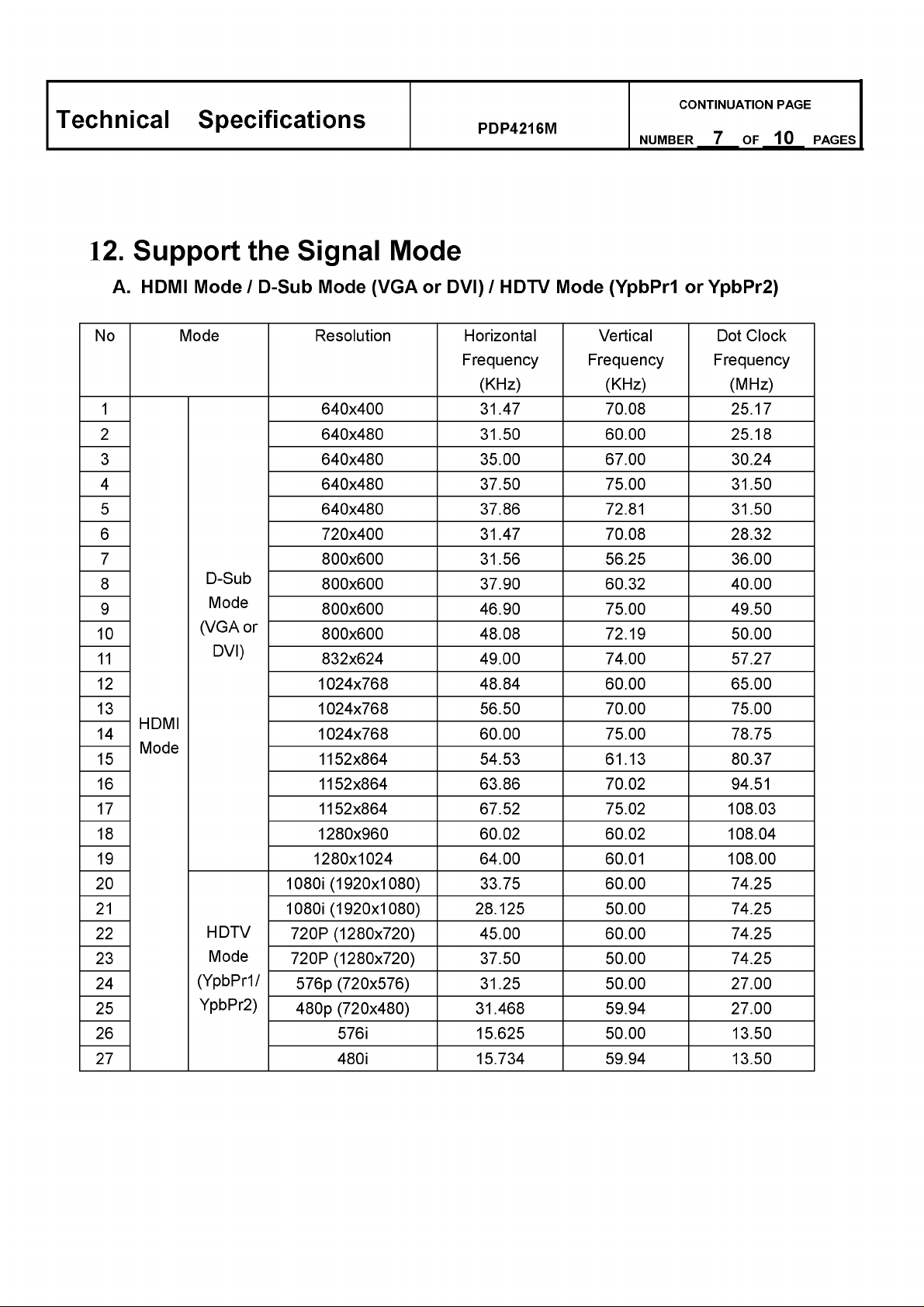
Technical Specifications
12. Support the Signal Mode
A . H D M I M o d e / D -S u b M o d e (V G A o r D V I) / H D T V M od e (Y p b P rl o r Y p b P r2 )
PDP4216M
CONTINUATION PAGE
NUMBER 7 OF 1 0 PAGES
No Mode Resolution Horizontal
Frequency
(KHz)
1 640x400 31.47 70.08 25.17
2 640x480 31.50 60.00 25.18
Vertical
Frequency
(KHz)
Dot Clock
Frequency
(MHz)
3 640x480 35.00 67.00 30.24
4 640x480 37.50 75.00 31.50
5 640x480 37.86 72.81 31.50
6 720x400 31.47 70.08 28.32
7 800x600 31.56 56.25 36.00
8
9
1 0
1 1
1 2 1024x768 48.84 60.00 65.00
13
HDMI
14 1024x768 60.00 75.00 78.75
Mode
15
D-Sub
Mode
(VGA or
DVI)
800x600 37.90 60.32 40.00
800x600 46.90 75.00 49.50
800x600 48.08 72.19 50.00
832x624 49.00 74.00 57.27
1024x768 56.50 70.00 75.00
1152x864 54.53 61.13 80.37
16 1152x864 63.86 70.02 94.51
17 1152x864 67.52 75.02 108.03
18 1280x960 60.02 60.02 108.04
19 1280x1024 64.00 60.01 108.00
2 0 1080i (1920x1080) 33.75 60.00 74.25
2 1 1080i (1920x1080) 28.125 50.00 74.25
2 2
23
24
25
HDTV
Mode
(YpbPr1/
YpbPr2)
720P (1280x720) 45.00 60.00 74.25
720P (1280x720) 37.50 50.00 74.25
576p (720x576) 31.25 50.00 27.00
480p (720x480) 31.468 59.94 27.00
26 576i 15.625 50.00 13.50
27 480i 15.734 59.94 13.50
Page 11

Technical Specifications
4 . 4 R e m o te C o n tr o l
1 POWER(cb): Press this button to turn off to
standby and turn on from standby.
2 MUTE(jc): Press this button to quiet the sound
system. Press again to reactivate the
sound system.
3 P.STILL: Press this button to hold on the
screen. Press again to normal.
4 P.SIZE: When the input source is YPbPr 1,
YPbPr 2, VGA or HDMI, press this button,
the picture will change according to Fill All,
Force 4:3, Letter Box, Wide or Anamorphic.
When the input source is AV or S-Video, press
this button, the picture will change according to
Fill All, 4:3, Letter Box, Wide or Anamorphic.
5 S.SELE: Press this button to select the sound
output from Main Window or Sub Window.
6 P.MODE : Press the button to select different
picture effect.
7 TIME: Press this button to pop up the "Clock
Set” menu.
8 SLEEP: Press this button to select the sleep
time.
9 INFO: Press the button to display the
source information.
10 AUTO: The Display automatically adjusts the
phase, vertical / horizontal position when
pressing this button in VGA mode.
11 LAYOUT: Press this button to pop up Layout
menu.
12 C/C: Press this button to enter the Closed
Caption Function. (Only for AV or S-Video)
13 V-CHIP: Press this button to enter the V-Chip
Function. (Only for AV or S-Video)
14 Number buttons: Use these buttons to enter
the password.
PDP4216M
CONTINUATION PAGE
NUMBER 8 OF 1 0 PAGES
2
5
6
9
10
12
13
14
18
19
22
23
25
(Continued on next page)
Page 12

Technical Specifications
PDP4216M
CONTINUATION PAGE
NUMBER 9 OF 10 PAGES
15 SWAP: Press this button to switch the Main
window or Sub window pictures in PIP and
Split Screen.
16 F.WHITE: Press this button to show a full
white picture.
17 PIP POS. : Press the button to select different
Image Position in PIP Mode.
18 PIP SIZE : Press the button to select different
Image Size in PIP Mode.
19 SPEAKER: Press this button to pop up the
"Speaker” menu, use the ^ / ► butt°n t° select
"Internal” or "External”.
20 SOUND: Press the button to select different
sound effect.
21 W.SELE: Press this button to select the Main
Window or Sub Window.
22 SOURCE: Press this button and use ▲ / T
button to select the signal sources. AV, S-Video,
YPbPr 1, YPbPr 2, VGA or HDMI.
23 PIP: Press this button to change different
Picture Mode.
24 MENU: Press this button to pop up the OSD
Menu and press it again to exit the OSD Menu.
25 OK : Press to enter or confirm.
26 -4 / ► : They are used as -4 / ► buttons in the
OSD Menu screen and they can be used for
the adjustment of volume when the OSD Menu
is not shown on the screen.
▲ / ▼ : They are used as ▲ / ▼ buttons in the
OSD Menu screen.
They also can be used for the selection of the
program when the OSD Menu is not shown on
the screen, but only for the Model with Tuner.
2
5
6
9
10
12
13
14
18
19
22
23
25
Page 13

Technical Specifications
P H Y S IC A L C H A R A C T E R IS T IC S
14. P o w er C o rd
PDP4216M
CONTINUATION PAGE
NUMBER 1 0 OF 10 PAGES
Length :
Type :
15. C a b in e t
15.1 Color :
15.2 Weight(W/Ostand)
Net weight :
Gross weight :
15.3 Dimensions
Width
Height
Depth
1.8m nominal
optional
black colour as defined by colour plaque reference number
34kg
(W/O stand&speak)
1024mm
692mm
286mm
Page 14

Block Diagram
Product Specification of PDP Module
LVDS Input
Control Signal
(Serial Interface)
APL Data
Vs(180V~190V)
Va(55V~65V)
Vcc(+5V)
Display data, Driver timing
Color Plasma Display Panel
1366 X 768 pixels
Address Driver
^ Applied Voltage level is specified at the time when Full-White pattern is displayed on the panel.
Page 15

Block Diagram MAIN / AUDIO BOARD
Page 16
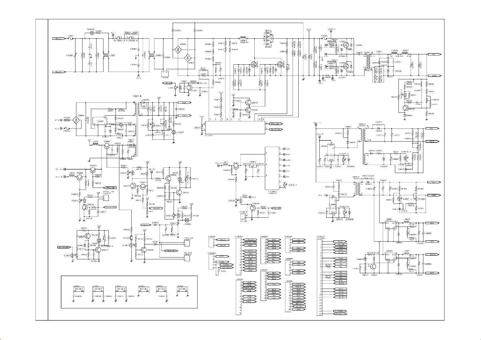
Circuit Diagram
- Power supply board o f A ud io A m p lif ier ,
- Main ( Vid e o) bo ard
- A u d io /T u n e r board
- Ke yp ad boa rd
- Remote co ntrol r ec eiv er board
- Rem ot e control board
Page 17

MPT 0 12 A
Page 18
Page 19

PT.T.1 8V OVDD3 3V#
Using digital interface:
DVdd (1.8V) (DVdd+CVdd) 130mA 234mW
PVd (1.8V) (PVd+ALVdd) 30mA 54mW
D D
B B
DDC SCL5 D S DDC SCL3
R919^ ^ J q 901
HSOUT
SOGOUT
VSOUT/AO
FIELD
DCLK
DDC5V 1
DDC SDA5
92
93
94
95
96
97
98
99
2 ADCB7
3 ADCB6
4 ADCB5
7 ADCB2
BO
88
DE
87
86
85
84
89
Ö R925
R920 °
D S
R924
ADC DCLK
Q902
R916 -
R929
l
R921
—
R922
Vd (3.3V) (Avdd+TVdd) 80mA 264mW
Vdd (3.3V) (Ovdd) 10-120mA, 30mA typical
99mW
Using analog interface:
TVDD3.3V
DVdd 60mA 108mW
PVd 20mA 36mW
DDC SDA3
Vd 270mA 891mW
C
MCLKIN
MCLKOUT
SCLK
LRCLK
1250
1251
1252
1253
A A
Title
9-HDMI-R
SizeBNumber Revision
Date: 14-O ct-2005 Sheet of
File:
F:\4228\4228 temp ddb\4228 Temp.DDB Drawn By:
Page 20

Page 21

Page 22

Page 23

Page 24

■ |c13Ö4 |c13Ö5 C1306 C1307 C1308 C130
T T TTTTT
2 L1304 VT5
4 II |+ IC1331 |C1330 |C1329 |C132
f t o i I I I J
— i c t-T
D
13 Ic1314 C1315 C1322 C1321 C1320 C1319 C1318 C1317 ^C131
TTTTTTTTT
3 C1334 C 1335 C1336 C1337 C1338 Cc1339 Cu340 'c1341 Cm 2 Cc134
A A
T
13-SCALER
I I
__
T TTT
Page 25

31RAMA0 40
31RAMA1 38
31RAMA2 36
31RAMA3 34
31RAMA4 33
31RAMA5 35
31RAMA6 37
31RAMA7 39
D D
5LOCK
31RAMA8 41
31RAMA9 43
31RAMA10 42
31RAMA11 45
31RAMA1246
31RAMA13 44
204
MA0
MD
MA1
MD
MA2
MD
MA3
MD
MA4
MD
MA5
MD
MA6
MA7
MA8
MA9
MA10
MA11
MA12
MA13
- MCLK MRAS
MCAS
MWE
U1201C
V33SW
MD9
MD8
MD7
MD6
MD5
MD4
67
6947
48 R121
49 R1217
50
31RAMD15
31RAMD14
31RAMD13
RAMD12
RAMD11
RAMD10
WE
17 31CASn
CAS
MM
'i iy iy o
¿QQ S
DQ10
DQ11
DQ12
DQ13
DQ14
DQ15
RAS
DQ0
DQ1
DQ2
DQ3
DQ4
DQ5
DQ6
DQ7
42
DQ8
44
DQ9
45
47
48
50
53
37
CKE
RAMD3
RAMD6
RAMD9
38
31RAMA0 23
31RAMA1 24
Cl242 C 1205 C1206 C1207 C1208 C12C
T TTTT^
ADR:0x64
B B
A A
- VSS0
- VSS1
104
VSS2
134
VSS3
- PVSS0
- PVSS1
53
PVSS2
79
PVSS3
91
PVSS4
122
PVSS5
147
PVSS6
78
76
123
ADDVSS PW1231P0WER .
29
- ADAVSS ADAVDD
32
- ADGVSS ADGVDD
- AVS33B AVD33B
- AVS33G AVD33G
- AVS33R AVD33R
4
- AVS33SVM AVD33SVM
VDD0
VDD1
VDD2
VDD3
PVDD0
PVDD1
PVDD2
PVDD3
PVDD4
PVDD5
PVDD6
70
V25SW
_T
V33SW1
146
AV25p1
----
AV25p2
AND GROUND
28 “ I AV25a
â=i_
22
AV331
_T
V33SW
T
__
C1210 C1212 C1213 C1214 C1215 C1216 C121
TTTTTT
V33SW1 V25SW AV25P1 V25SW
C1227 C1228 C1229 C1230 C1231 C1232 C123
C1247 C1246
‘TTTTTTT
X F I | 221 C 122
’ITTTT
C1234 C1235 C1:
' I X -
AV25A V33SW
C1250
C1237 C1238 C1239 C 124
'TTTT
C1224 C1:
X
31RAMA2 25
31RAMA3 26
31RAMA4 29
31RAMA5 30
31RAMA6 31
31RAMA7 32
31RAMA8 33
31RAMA9 34
31RAMA10 22
31RAMA11 35
31RAMA12 20
31RAMA13 21
B
Date: 14-0ct-2005
File: F:\4228V4228 tempddb\4228 Temp.DDB Drawn B
U1203
A0
A1
A2
A3
A4
A5
A6
A7
A8
A9
A10
A11
12-DEINTERLACE
Number Revisi
C
Page 26

Page 27

I. * T
RSTINn 2
TLCCT 3
U403
SENCE Vdd
RESin
RESET
CT
____
RESET
CONTROL
ADR:0xA0/MEMORY
ADR:0xD0/ COMPANION
RESETn
GND
R406
D
R422
A A
T
4-FLASH
Numb
A3
F:\4228\4228 temp ddb\4228 Temp.DDBDrawn By:
et of
Page 28

4
For sumsung panel standard LVD S jack
TX0
D D
TX1
TX2
12
CK
16
TX3
20 501 502
C C
NC
For sumsung panel
DRE0
DRE1
DRE2
DRE3
DRE4
DRE5
DRE6
DRE7
B B
DGE0
DGE1
DGE2
DGE3
DGE4
DGE5
DGE6
DGE7
DB E0
DBE1
DB E2
DBE3
DB E4
DBE5
DB E6
DB E7
A A
DR E[7..0t »
DG E[7 ..0H
DB Ef7..0 l>
DHS
DVS
DEN
LVD33
T
_
DHS 27
DVS 28
< DEN 30
>
L501
For LG panel
DRE2 51
DRE3 52
DRE4 54
DRE5 55
DRE6 56
DRE7
DRE0
DRE1 2
x
DGE2 4
S
DGE3 6
s
DGE4 7
s
DGE5 11
s
DGE6 12
s
DGE7 14
s
DGE0 8
\
DGE1 10
DBE2 15
s
DBE3 19
s
DBE4 20
s
DBE5 22
s
DBE6 23
s
DBE7 24
s
DBE0 16
\
DBE1 18
—j —C520 — — C522 —j—C
LVD_V
—I— C
JÜ
-C523 —1— C525
"L
RS
I
d
s
31
50
I - 0
K
V
TxIN0
TxIN1
TxIN2 TxOUT0+
TxIN3 TxOUT1-
TxIN4 TxOUT1+
TxIN6 TxOUT2-
TxIN27 TxOUT2+
TxIN5 TxOUT3-
TxIN7 TxOUT3+
TxIN8 TxCLKOUT-
TxIN9 TxCLKOUT+
TxIN12
TxIN13
TxIN14
TxIN10 PWR DWN
TxIN11
TxIN15
TxIN19
TxIN20 PL L GND
TxIN21 PLL GND
TxIN22
TxIN16
TxIN17 LVDS GND
TxIN24 LVDS GND
TxIN25 LVDS GND
TxIN26
TxIN23
U501
/ DS90C385AMTD
L504
i
_
R504
TX0- 1 2
TX0+ 3
TX1- 5 6 P SCLK
TX1+ 7
TX2- 9
TX2+ 11
CK- 13 4 P SCLK#
CK+ 15
TX3+ 19
C
C
C
C
C
C
V
VCC
V
V
S
L
D
PL TxOUT0-
V
L
R FB
GND
GND
GND
GND
O
4
8
P SDATA# P SLE
P SLE#
P DISPEN#TX3- 17 P DISPEN
20
— SCL S3V
— SD A S3V )
For LG panel standard LVD S jac k
TX0-
TX1-
TX2-
CK-
TX3- 11
1
10
12
13
14
PDPGO
I.
p dispen# 27
p sdata#
p sclk#
29
I sle#
30
31
NC SGND
Title
Size
Number Revision
A4
Date: 14-Oct-2005 Sheet of
File: F:\4228\4228 temp ddb\4228 Temp.DDI 5 Drawn By: ANDY
rY YTV.
C527
R513
______
l _ L 505o
—I— C528
I
L506
IRQ
X
L503
YTYYV
- I -
r
INPUT OUTPUT
O
5-LVDS&TMDS
Formosa panel CPUGO
---------(r e La y o n # I
P SDATA
Formosa panel PDPGO
---------( V s on # I
P SCLK
TAB
P SDATA
P SLE
P DISPEN
00
Page 29

Page 30

Page 31

Audio.Board.BH(M-CH).05.06.14.sch-1 - Tue Aug 16 22:15:14 2005
Page 32

DUBHE OSD Ver1.1 NAKS.sch-1 - Mon Oct 1B 11:47:11 2004
Page 33

R702
56K
- w -
REMOTE PCB
VD701
IN4148
X°“ l
O K51
X°~l
OK47
<?K48
^O—11
9K44
✓o-hI
^K43
✓O—11
QK 36 gK35
X°n
£ K 5 0
^O-i i
£K46
^Ohi
^K42
✓ O -o
£K38
^ O - o
gK34
✓ ° i
OK49
/'CHI
OK45
fO-ii
Q K41
^O—< I
OK37
^CHI
gK33
✓ ° 1
OK32
QK 28
p/ O—< I
OK24
yo-<>
gK20
£k16
^ O - H
gK 1 2
✓ O h >
gK8
^ C H I
g K 4
0K31
yo->>
gK27
fO-o
~ K19
^ O H I
~K15
ycxi
~*K11
yen i
>K7
^ O -o
g K3
^/O-i /'O-i
OK30 OK29
gK26
gK25
✓ C H »
^/Ohi
gK22
gK21
^ C H i
gK 18
£ K 1 7
yo~> >
g K13
^CH I
gK10
✓ O h »
£ K 6
gK 5
✓CH I
^/Ohi
_gK2
g K1
»
- 2 ±
LL
JÄ.
J£.
JZ.
ja.
ja .
¿a.
21
22.
21
N701
PT2222
_ rv
X L .
€702
150pF
□
G701 'i ^ n ,
455KHZ
a 150pF
B701
BT701
3V
H'l
C701
^7U /10 V
+ 0 —
R701?701<
A°wf
V701
80 50
Page 34

REMOTE CONTROL CODE ASSIGNMENT
KEY NO. KEY NAME DATA CODE KEY NO. KEY NAME DATA CODE
K1 POWER 00 K33 dumb 40
K2
K3
K4
K5 P.MODE 04 K37
K6
K7 5 06 K39 nil 46
K8
K9
K10 7 09 K42 PREV 49
K11 8 OA K43 P.STILL 4A
K12 9 OB K44 SOUND 4B
K13 MTS OC K45 SLEEP 4C
K14 nil OD K46
K15
K16
K17
K18
K19
K20
K21 MENU 14 K53 nil 54
K22
K23
K24
K25 0 18 K57 nil 58
K26
K27
K28 EXIT 1B K60 nil 5B
K29 PIP 1C K61 nil
K30
K31
K32 PIP CH+ 1F K64
1
2 02 K35
3
4
6
nil
S.SELE
OK
CH.+
VOL.+
VOL .-
CH .- 13 K52 nil 53
Source
nil
P.SIZE
F.White
PIP Source
SWAP
PIP CH-
01 K34
03 K36 dumb 43
05 K38
07 K40 nil 47
08 K41 100 48
OE K47 Picture 4E
OF K48 CH Erase 4F
10 K49
11 K50 C/C 51
12 K51
15 K54 nil 55
16 K55 nil 56
17 K56
19 K58
1A K59 nil 5A
1D K62 nil 5D
1E K63 nil 5E
dumb
dumb
MUTE
INFO
TIME
CH Save
V-CHIP
nil
nil
nil
41
42
44
45
4D
50
52
57
59
5C
5F
CUSTOM CODE: 20DD
00 25. sch -1 - Mon May 16 09:25:50 2005
FOR NTSC
Page 35

Basic Operations & Circuit Description
MODULE
There are 1 pc. panel and 12 pc.s PCB including 2 pc.s Y/Z Sustainer board, 2 pc.s Y Drive
board, 6 pc.s X Extension boards, 1 pc. Control (Signal Input) and 1 pc. Power
board in the Module.
SET
There are 6 pc.s PCBs including 1 pc. AUX. PSU Board, 1 pc. Keypad board, 1 pc.
Remote Control Receiver board, 1 pc. L/R Speakers and 1 pc. Main (Video) board in the SET.
Page 36

Y-d w er TOP
E-extension Top
L/C/R
Control Board Assay Power supple
Internal Speaker
terminal
Y-sustainer
Y-driver Bottom
Z-sustainer
Local Key
Stand
Main ( Video) Turner/Audio
X-extension
Bottom L/C/R
Page 37

PCB function
1. Power:
(1). Input voltage: AC 100V~120V, 45Hz~60Hz.
Input range: AC 90V(Min)~265V(Max) auto regulation.
(2). To provide power for PCBs.
2. Main (Video InterFace) board: To converter TV signals, S signals, AV signals, Y Pb/
Cb Pr/Cr signals, DVI signals and D-SUB signals to digital ones and to transmit to
Control board.
3. Control board: Dealing with the digital signal for output to panel.
4. Y-Sustainer / Z-Sustainer board:
(1). Receiving the signals from Control and high voltage supply.
(2). Output scanning waveform for Module.
5. Y-Drive board: Receive signal from Y sustainer, output horizontal scanning wave
form to the panel.
6. X extension board (6pcs): Output addressing signals.
7. Tuner/Audio Board: Process and Amplifying the audio signal to speakers and
convert TV RF signal to video/audio signal and send to Main board.
Page 38

PCB failure analysis
1. CONTROL
2. MAIN (video) :
3. POWER
4. Z - Sustainer
5. Y - Sustainer
6. X - Extension : Abormal vertical noise on screen.
7. Audio Board or AUX PSU: a. No voice. (Make sure Mute/OFF)
: a. Abnormal noise on screen. b. No picture.
a. Lacking color, Bad color scale.
b. No voice.
c. No picture but with signals output, OSD and back light.
d. Abnormal noise on screen.
: No picture, no power output.
:a. No picture.
b. Color not enough.
c. Flash on screen.
: Darker picture with signals.
b. Noise.
Page 39

Basic operation of Plasma Display
1. After turning on power switch, power board sends 5Vst-by Volt to Micro Processor
2. The micro Processor memorize the last state of Power, When the last state of
power is on or receive power on signal from local Key or Remote control, Micro
Processor will send on control signal to power. Then Power sends (5Vsc, 9Vsc,
24V and RLYON, Vs ON) to PCBs working. This time VIF will send signals to
display Image, OSD on the panel and start to search available signal sources.
If the audio signals input, them will be amplified by Audio AMP and transmitted to
Speakers.
3. If some abnormal signals are detected (for example: over volts, over current, over
temperature and under volts), the system will be shut down by Power off.
Page 40

Main IC Specifications
- PW181 Image Processor, Scaler
- PW1231 Digital Video Signal Processor
- VPC 323XD Comb-filter Video Processor
- Z86229 NTSC Line 21 CCD decorder
- MSP34x0G Multistandard Sound Processor
-AD9880 Analog/HDMI Dual Display Interface
-PI5V330 Wideband/Video Quad 2-Channel MUX/DEMUX
-SM5304AV Video Buffer with Built-in Analog LPF
-TDA2616 2 X 12 W hi-fi audio power amplifier with mute
-SAA5360 Multi page intelligent teletext decoder
-AT24C32 Z-Wire Serial EEPROM
-HT48R06A-1 8-Bit Cost-Effective I/O Type MCU
Page 41

PW181
Product Specification
General Description
The PW181 ImageProcessor is a highly integrated
“system-on-a-chip” that interfaces computer graphics and
video inputs in virtually any format to a fixed-frequency flat
panel display.
Computer and video images from NTSC/PAL to WUXGA
at virtually any refresh rate can be resized to fit on a fixed-
frequency target display device with any resolution up to
WUXGA. Video data from 4:3 aspect ratio NTSC or PAL
and 16:9 aspect ratio HDTV or SDTV is supported. Multi
region, nonlinear scaling allows these inputs to be resized
optimally for the native resolution of the display.
Advanced scaling techniques are supported, such as
format conversion using multiple programmable regions.
Three independent image scalers coupled with frame
locking circuitry and dual programmable color lookup
tables create sharp images in multiple windows, without
user intervention.
Embedded SDRAM frame buffers and memory controllers
perform frame rate conversion and enhanced video
processing completely on-chip. A separate memory is
dedicated to storage of on-screen display images and
CPU general purpose use.
Advanced video processing techniques are supported
using the internal frame buffer, including motion adaptive,
temporal deinterlacing with film mode detection. When
used in combination with the new third-generation scaler,
this advanced video processing technology delivers the
highest quality video for advanced displays.
Both input ports support integrated DVI 1.0 content
protection using standard DVI receivers.
A new advanced OSD Generator with more colors and
larger sizes supports more demanding OSD applications,
such as on-screen programming guides. When coupled
with the new, faster, integrated microprocessor, this OSD
Generator supports advanced OSD animation techniques.
Video
TV
Signal
TV
Signal
Input
TV Tuner
Com pute r
Com pute r
j TV Tuner j
Video
Input
Video
Decoder
ADC/
TMDS
ADC/
TMDS
r 1
Video
Decoder
PW181 System Block Diagram
Crystal
~ r
PW181
ROM
Features
• Third-generation, tw o-dimensional filtering techniques
• Third-generation, advanced scaling techniques
• Second-generation Automatic Image Optimization
• Fram e rate conversion
• Video processing
• On-Screen Display (OSD)
• On-chip microprocessor
• JTAG debugger and boundary scan
• Picture-in-picture (PIP)
• M ulti-region, non-linear scaling
• Hardware 2-wire serial bus support
Applications
• M ultim edia Displays
• Plasma Displays
• Digital Television
Device Application Package
PW181-10V Up to XGA Displays
PW181-20V Up to UXGA Displays
352 PBGA
Dis p lay
Programmable features include the user interface, custom
start-up screen, all automatic imaging features, and
special screen effects.
pixelworks
8100 SW Nyberg Road
Tualatin, OR 97062 USA
Telephone: 503.454.1750
FAX: 503.612.0848
www.pixelworks.com PRELIMINARY I CONFIDENTIAL
Page 42

AN A LO G 110 MSPS/140 MSPS Analog Interface
►
FEATURES
140 MSPS Maxim um Conversion Rate
300 MHz Analog Bandwidth
0.5 V to 1.0 V Analog Input Range
500 ps p-p PLL Clock Jitter at 110 MSPS
3.3 V Power Supply
Full Sync Processing
Sync Detect for “ Hot Plugging”
Midscale Clamping
Power-Down Mode
Low Power: 500 mW Typical
4:2:2 Output Format Mode
APPLICATIONS
RGB Graphics Processing
LCD Monitors and Projectors
Plasma Display Panels
Scan Converters
Microdisplays
Digital TV
DEVICES for Flat Panel Displays
AD9883A
FUNCTIONAL BLOCK DIAGRAM
GENERAL DESCRIPTION
The AD9883A is a complete 8-bit, 140 MSPS monolithic analog
interface optimized for capturing RGB graphics signals from
personal computers and workstations. Its 140 M SPS encode
rate capability and full power analog bandwidth of 300 MHz
supports resolutions up to SXGA (1280 x 1024 at 75 Hz).
The A D9883A includes a 140 MHz triple ADC with internal
1.25 V reference, a PLL, and programmable gain, offset, and
clamp control. The user provides only a 3.3 V power supply,
analog input, and Hsync and CO A ST signals. Three-state
CMO S outputs may be powered from 2.5 V to 3.3 V.
The AD9883A’s on-chip PLL generates a pixel clock from the
Hsync input. Pixel clock output frequencies range from 12 MHz to
140 MHz. PLL clock jitter is 500 ps p-p typical at 140 MSPS.
When the COAST signal is presented, the P LL maintains its
output frequency in the absence of Hsync. A sampling phase
adjustment is provided. Data, Hsync, and clock output phase
relationships are maintained. The AD9883A also offers full sync
processing for composite sync and sync-on-green applications.
A clamp signal is generated internally or may be provided by
the user through the CLAMP input pin. This interface is fully
programmable via a 2-wire serial interface.
Fabricated in an advanced CMOS process, the AD9883A is
provided in a space-saving 80-lead LQFP surface-mount plastic
package and is specified over the 0°C to 70°C temperature range.
REV. A
Information furnished by Analog Devices is believed to be accurate and
reliable. However, no responsibility is assumed by Analog Devices for its
use, nor for any infringements of patents or other rights of third parties that
may result from its use. No license is granted by implication or otherwise
under any patent or patent rights of Analog Devices.
One Technology Way, P.O. Box 9106, Norwood, MA 02062-9106, U.S.A.
Tel:
Fax:
Page 43

PW1231A
Product Specification
General
The PW1231A is a high-quality, digital video signal
processor that incorporates Pixelworks' patented
deinterlacing, scaling, and video enhancement
algorithms. The PW1231A accepts industry-standard
video formats and resolutions, and converts the input into
many desired output formats.The highly efficient video
algorithms result in excellent quality video.
The PW1231A combines many functions into a single
device, including a memory controller, auto-configuration,
and others. This high level of integration enables simple,
flexible, cost-effective solutions that require fewer
components.
Crystal
Video
PW1231A
System Block Diagram
Video
Decoder
PW1231A
PW1231AL
SD RAM
Digital
Output
Features
• Built-In Memory Controller
• Motion-Adaptive Deinterlace Processor
• Intelligent Edge Deinterlacing
• Digital Color/Luminance Transient Improvement (DCTI/DLTI)
• Interlaced Video Input Options, including NTSC and PAL
• Independent horizontal and vertical scaling
• Copy Protection
• Two-Wire Serial Interface
Applications:
For use with Digital Displays
• Flat-Panel (LCD, DLP) TVs
• Rear Projection TVs
• Plasma Displays
• LCD Multimedia M onitors
• Multimedia Projectors
Device Application Package
PW1231A
PW1231AL
NOTE: “L” denotes lead (Pb) free
Up to XGA 160-pin PQF
pixelworks
8100 SW Nyberg Road
Tualatin, OR 97062 USA P/N 001-0097-00 Rev B
Telephone: 503.612.6700 July 2003
ww w ^xelwo i^s.com PRELIMINARY CONFIDENTIAL
Page 44

ANALOG
DEVICES Analog/HDMI Dual Display Interface
□
Preliminary Datasheet
FEATU R E S
Analog/HDMI Dual Interface
Supports High-Bandwidth Digital Content Protection
RGB to YCbCr two-way color conversion
Automated clamping level adjustment
1.8/3.3V Power Supply
100-pin LQFP Pb-Free Package
RGB and YCbCr Output Formats
Analog Interface
8-bit Triple Analog to Digital Converters
150 M SPS Maximum Conversion Rate
Macrovision Detection
2:1 Input Mux
Full Sync Processing
Sync Detect for “Hot Plugging”
Mid-Scale Clamping
Digital Video Interface
HDMI 1.0, DVI 1.0
150 MHz HDMI Receiver
Supports High-Bandwidth Digital Content Protection
(HDCP 1.1)
Digital Audio Interface
HDMI 1.0 compatible audio interface
S/PDIF (IEC90658 compatible) digital audio output
Multi-channel I2S audio output (up to 8 channels)
_____
FUNCTIONAL B LO CK DIA GRAM
3/26/2004 AD9880
APPLICATIONS
Advanced TV
HDTV
Projectors
LCD Monitor
GENERAL DESCRIPTION
The AD9880 offers designers the flexibility of an analog interface
and High-Definition Multimedia Interface (HDMI) receiver
integrated on a single chip. Also included is support for High
bandwidth Digital Content Protection (HDCP).
Analog Interface
The A D9880 is a complete 8-bit 150 M SPS monolithic analog
interface optimized for capturing Component Video (YPbPr) and
RGB graphics signals. Its 150 MSPS encode rate capability and
full power analog bandwidth of 300 MHz supports all HDTV
formats (up to 1080p) and FPD resolutions up to SXGA (1280 x
1024 at 75 Hz).
The analog interface includes a 150 MHz triple ADC with
internal 1.25 V reference, a Phase Locked Loop (PLL), and
programmable gain, offset, and clamp control. The user provides
only 1.8V and 3.3V power supply, analog input, and Hsync.
Three-state CM OS outputs may be powered from 1.8V to 3.3V.
The A D 9880’s on-chip PLL generates a pixel clock from Hsync.
Pixel clock output frequencies range from 12 MHz to 150 MHz.
AD9880 Preliminary Technical Information
Informa tio n f urnished by An alog D evices is b eliev ed to be accurate an d reliab le.
Ho wever, no respon sibility is assu m ed by An alog D ev ices for it s use, nor for a ny
infrin gem ents of pa tents o r other rig hts o f third parties whic h may result fro m its
use. N o lice nse is granted by implication or o therwise u nder an y pate nt or pate nt
rig hts of Analog De vices.
PL L clock jitter is typically less than 500 ps p-p at 150 MHz. The
AD9880 also offers full sync processing for composite sync and
Sync-on-Green (SOG ) applications.
Digital Interface
The AD9880 contains a HDMI 1.0 compatible receiver and
supports all HDTV formats (up to 1080p) and display resolutions
up to SXG A (1280 x 1024 at 75 Hz). The receiver features an
intra-pair skew tolerance of up to one full clock cycle. With the
inclusion o f HDCP, displays may now receive encrypted video
content. The AD9880 allows for authentication of a video receiver,
decryption of encoded data at the receiver, and renewability of that
authentication during transmission as specified by the HDCP 1.1
protocol.
Fabricated in an advanced CMOS process, the AD9880 is provided
in a space-saving 100-lead LQFP surface-mount plastic package
and is specified over the 0 °C to 70 °C temperature range.
© Analog Devices, Inc., 2004
One T e chno lo g y W ay, P .O Box 9106, N orw o od, M A 0 206 2-910 6, U SA
Te l: 617 /3 29-47 00 Fa x: 617 -3 2 6-8 703
Page 45

PRELIMINARY DATA SHEET VPC 323xD
Com b F ilter Video P rocessor
1. In troduction
The VPC 323xD is a high-quality, single-chip video
front-end, which is targeted for 4:3 and 16:9, 50/60-Hz
and 100/120 Hz TV sets. It can be combined with other
members of the DIGIT3000 IC family (such as
DDP 331x) and/or it can be used with 3rd-party prod
ucts.
The main features of the VPC 323xD are
- high-performance adaptive 4H comb filter Y/C sepa
rator with adjustable vertical peaking
- multi-standard color decoder PAL/NTSC/SECAM
including all substandards
- four CVBS, one S-VHS input, one CVBS output
- two RGB/YCrCb component inputs, one Fast Blank
(FB) input
- integrated high-quality A/D converters and associ
ated clamp and AGC circuits
- multi-standard sync processing
- linear horizontal scaling (0.25 ... 4), as well as
non-linear horizontal scaling ‘Panoramavision'
- PAL+ preprocessing
- peaking, contrast, brightness, color saturation and
tint for RGB/YCrCb and CVBS/S-VHS
- high-quality soft mixer controlled by Fast Blank
- PIP processing for four picture sizes (1-, 1-,
36 of normal size) with 8 -bit resolution
1 6 , or
- 15 predefined PIP display configurations and expert
mode (fully programmable)
- control interface for external field memory
- I2 C-bus interface
- one 20.25-MHz crystal, few external components
- 80-pin PQFP package
1.1. System A rchitecture
Fig.1-1 shows the block diagram of the video proces
sor
- line-locked clock, data and sync, or 656-output
interface
c i n o
VIN1 O
V IN 2 0
V IN 3 0
VIN40-
VOUTO
RGB/
YCrCb
FB O
RG B/q -
YCrCb
Y OUT
LL C ock
H Sync
V Sync
AVO
Fig. 1 -1: Block diagram of the VPC 323xD
Micronas
HDH
20.25 MHz I2C Bus
Page 46

O
o
Pr e l im in a r y Pr o d u c t Sp e c ifica t ion
Z86229
N
Totally Logical
FEATURES
Speed Pin Count/ Standard On-Screen Display Program
Devices (MHz) Package Types Tem p. Range & Closed Captioning Rating Tim e of Day
Z86229 V2 18-Pin DIP, SOIC 0°C to +70°C Yes Yes Yes
N TS C Line 21 C CD D e c od er
Automatic Data Extraction
Complete Stand-Alone Line 21 Decoder for Closed-
Captioned and Extended Data Services (XDS)
Preprogrammed to Provide Full Compliance with
EIA-608 Specifications for Extended Data Services
Automatic Extraction and Serial Output of Special
XDS Packets (Time of Day, Local Time Zone, and
Program Blocking)
Programmable XDS Filter for a Specific XDS Packet
Cost-Effective Solution for NTSC Violence Blocking
inside Picture-in-Picture (PiP) Windows
GENERAL DESCRIPTION
Capable of processing Vertical Blanking Interval (VBI)
data from both fields of the video frame in data, the Z86229
Line 21 Decoder offers a feature-rich solution for any tele
vision or set-top application. The robust nature of the
Z86229 helps the device conform to the transmission format
defined in the Television Decoder Circuits Act of 1990, and
in accordance with the Electronics Industry Association
specification 608 (EIA-608).
The Line 21 data stream can consist of data from several data
channels multiplexed together. Field 1 consists of four data
channels: two Captions and two Texts. Field 2 consists of
five additional data channels: two Captions, two Texts, and
Extended Data Services (XDS). The XDS data structure is
Minimal Communications and Control Overhead Pro
vide Simple Implementation of Violence Blocking,
Closed Captioning, and Auto Clock Set Features
Programmable, On-Screen Display (OSD) for Creat
ing Full Screen OSD or Captions inside a Picture-in-
Picture (PiP) Window
User-Programmable Horizontal Display Position for
easy OSD Centering and Adjustment
I2C Serial Data and Control Communication
Supports 2 Selectable I C Addresses
defined in EIA-608. The Z86229 can recover and display
data transmitted on any of these nine data channels.
The Z86229 can recover and output to a host processor via
the I2C serial bus. The recovered XDS data packet is further
defined in the EIA-608 specification. The on-chip XDS fil
ters in the Z86229 are fully programmable, enabling recov
ery of only those XDS datapackets selected by the user. This
functionality allows the device to extract the required XDS
information with proper XDS filter setup for compatibility
in a variety of TVs, VCRs, and Set-Top boxes.
In addition, the Z86229 is ideally suited to monitor Line 21
video displayed in a PiP window for violence blocking,
CCD, and other XDS data services. A block diagram of the
Z86229 is illustrated in Figure 1.
DS005103-0601
Page 47

PRELIMINARY DATA SHEET
MSP 34xOG
Multista n dard Sound Processor Family
Rele ase Note: R e vision bars indic a te significant
chang e s to th e previous edition. The h ardware and
softw are descrip tion in this d ocum en t is valid for
th e MS P 34xOG version B8 and following versions.
1. Introduction
The MSP 34xOG family of single-chip Multistandard
Sound Processors covers the sound processing of all
analog TV-Standards worldwide, as well as the NICAM
digital sound standards. The full TV sound processing,
starting with analog sound IF signal-in, down to pro
cessed analog AF-out, is performed on a single chip.
Figure 1-1 shows a simplified functional block diagram
of the MSP 34xOG.
This new generation of TV sound processing ICs now
includes versions for processing the multichannel tele
vision sound (MTS) signal conforming to the standard
recommended by the Broadcast Television Systems
Committee (BTSC). The DBX noise reduction, or alter
natively, Micronas Noise Reduction (MNR) is per
formed alignment free.
Other processed standards are the Japanese FM-FM
multiplex standard (EIA-J) and the FM Stereo Radio
standard.
Current ICs have to perform adjustment procedures in
order to achieve good stereo separation for BTSC and
EIA-J. The MSP 34xOG has optimum stereo perfor
mance without any adjustments.
All MSP 34xxG versions are pin compatible to the
MSP 34xxD. Only minor modifications are necessary
to adapt a MSP 34xxD controlling software to the
MSP 34xxG. The MSP 34xOG further simplifies con
trolling software. Standard selection requires a single
l2C transmission only.
The MSP 34xOG has built-in automatic functions: The
IC is able to detect the actual sound standard automat
ically (Automatic Standard Detection). Furthermore,
pilot levels and identification signals can be evaluated
internally with subsequent switching between mono/
stereo/bilingual; no l2C interaction is necessary (Auto
matic Sound Selection).
The MSP 34xOG can handle very high FM deviations
even in conjunction with NICAM processing. This is
especially important for the introduction of NICAM in
China.
The ICs are produced in submicron CMOS technology.
The MSP 34xOG is available in the following packages:
PLCC68 (not intended for new design), PSDIP64,
PSDIP52, PQFP80, and PLQFP64.
Sound IF1 o-
Sound IF2 &
SCART3
SCART4
MONO »
Fig. 1-1: Simplified functional block diagram of the MSP 34xOG
Loud
speaker
Sound
Processing
Headphone
Sound
Processing
DAC
DAC
DAC
DAC
SCART
Output
Select
Loud
C
speaker
«0 Subwoofer
Headphone
SCART1
c
SCART2
c
Micronas
Page 48

f ù P E R I C O M
PI5V330
iiiiiiiiiiiiiiiiiiiiiiiiiiiiiiiiiiiiiiiiiiiiiiiiiiiiiiiiiiiiiiiiiiiiiiiiiiiiiiiiiiiiiiiiiiiiiiiiiiiiiiiiiiiiiiiiiiiiiiiiiiiiiiiiiiiiiiiiiii
Low ON Resistance Wideband/Video
Quad 2-Channel MUX/DEMUX
Product Features:
• High-performance, low-cost solution to switch
between video sources
• Wide bandwidth: 200 MHz
• Low ON-resistance: 30.
• Low crosstalk at 10 MHz: -58 dB
• Ultra-low quiescent power (0.1 typical)
• Single supply operation: +5.0V
• Fast switching: 10 ns
• High-current output: 100 mA
• Packages available:
- 16-pin 300-mil wide plastic SOIC (S)
- 16-pin 150-mil wide plastic SOIC (W)
- 16-pin 150-mil wide plastic QSOP (Q)
Functional Block Diagram
Product Description:
Pericom Semiconductor’s PI5V series of mixed signal video
circuits are produced in the Company’s advanced CMOS
low-power technology, achieving industry leading perfor
mance.
The PI5V330 is a true bidirectional Quad 2-channel
multiplexer/demultiplexer that is recommended for both
RGB and composite video switching applications. The
VideoSwitch™ can be driven from a current output
RAMDAC or voltage output composite video source.
Low ON-resistance and wide bandwidth make it ideal for
video and other applications. Also this device has exception
ally high current capability which is far greater than most
analog switches offered today. A single 5 V supply is all that
is required for operation.
The PI5V330 offers a high-performance, low-cost solution
to switch between video sources. The application section
describes the PI5V330 replacing the HC4053 multiplier and
buffer/amplifier.
Truth Table
EN IN
0 0
0 1 S2a, S2b, S2c, S2d
1 X
ON Switch
S1a, S1b, S1c, S1d
Disabled
16-Pin Product Configuration
1 16
S1A
S2A
DA
S1B
S2B
DB
GND
IN
2 15
3 14
4
5
6
7
8 9
16-PIN
Q16
S16
W 16
VCC
EN
S1D
13
S2D
12
DD
11
S1C
10
S2C
DC
Product Pin Description
Pin Name
S1a, S2a Analog Video I/O
S1b, S2b
S1c, S2c
S1d, S2d
IN
EN
Da, Db, Analog Video I/O
Dc, Dd
GND
Vcc Power
Description
Select Input
Enable
Ground
1
P S70 3 2C 0 8 /0 7/9 7
Page 49

SM5304AV
WPC
NIPPON PRECISION CIRCUITS INC.
OVERVIEW
The SM5304AV is a 75ii terminating resistance drive video buffer with built-in analog filter. The filter cutoff
frequency, controlled by the resistance connected to RFC pin, can be set to match any system resolution. The
output buffer can be selected OdB, 6dB, and 12dB. The feedback point occurs after the external coupling
capacitors, and the coupling capacitances can be reduced.
Video Buffer with Built-in Analog LPF
FEATURES
■ 5V ± 10% supply voltage
■ Adjustable cutoff frequency using external resistor
■ OdB, 6dB, 12dB selectable gain using logic signal
■ ± 0.5dB output gain error
■ TWo systems (two load resistances) can be driven
■ 0.7% output signal harmonic distortion
■ Sag compensation circuit built-in
■ Package: 8-pin VSOP (Pb free)
APPLICATIONS
■ DVD
■ Digital still camera
■ Digital VHS
ORDERING INFORMATION
Device Package
SM53Q4AV
8-pir VSO P
PINOUT
(Top view)
vin | - r
ENABLE[^ 2
RFC
VCC |~4~
•
PACKAGE DIMENSIONS
(Unit: mm)
Weight: 0.04g
8 I GSEL
H I VF
I VOUT
5 I GND
NIPPON PRECISION CIRCUITS INC.— 1
Page 50

BLOCK DIAGRAM
PIN DESCRIPTION
SM5304AV
vcc
GND
Number
1 VIN I A
2
3 RFC
4 VCC
5 GND
6 VOUT
7 VF I A Output signal feedback pin for sag compensation circuit
B GSEL I D
1. I: input, 0: output
2. k . analog, D. digital
Name I/O1 uuP Description
Input signal pin
ENABLE I D ,
0 A
- -
-
0 A Output signal pin
-
Enable signal input pin (wrtti pull-down resistor)
LPF cutoff frequency set pin
5V supply pin
Ground pin
Gain set signal input pin
NIPPON PRECISION CIRCUITS INC.—2
Page 51

Philips Semiconductors
Product specification
2 x 12 W hi-fi audio power amplifiers
TDA2616/TDA2616Q
with mute
FEATURES
• Requires very few external components
• No switch-on/switch-off dicks
• Input mute during switch-on and switch-off
• Low offset voltage between output and ground
• Excellent gain balance of both amplifiers
• Hi-fi in accordance with I EC 268 and DIN 45500
• Short-circuit proof and thermal protected
• Mute possibility.
QUICK REFERENCE DATA
Stereo application
SYMBOL PARAMETER CONDITIONS
±Vp supply voltage range 7.5 - 21 V
Po
Gv internal voltage gain -
|GVI
a
output power VP = +16 V; THD = 0.5%
channel unbalance
channel separation
SVRR supply voltage ripple rejection -
Vno
noise output voltage
GENERAL DESCRIPTION
The TDA2616 and TDA2616Q are dual power amplifiers.
The TDA2616 is supplied in a 9-iead single-in-line (SI 19)
plastic power package (SOU 31), while theTDA2616Q is
supplied in a 9-lead SI L-bent-toDIL plastic power package
(SOT157). They have been especially designed far mains
fed applications, such as stereo radio and stereo TV.
MIN. TYP. MAX.
-
12 - w
30 - dB
-
-
0.2
-
70 - dB
60 - dB
- 70 -
UNIT
dB
jlV
ORDERING INFORMATION
EXTENDED TYPE
NUMBER
PINS
TDA2616 9 SIL
TDA2616Q
Notes
1. SOT131-2; 1996 August 27.
2. SOT157-2; 1996 August 27.
PACKAGE
PIN POSITION
MATERIAL CODE
plastic
9 SIL-bent-to-DIL plastic
SOT131<1)
SOT157<2>
Page 52

Philips Semiconductors Product specification
2 x 12 W hi-fi audio power amplifiers with JDA2616/TDA2616Q
mute
+ v p
Fig. 1 Block diagram.
Page 53

Philips Semiconductors
Product specification
Multi page intelligent teletext decoder
1 FEATURES
• Support for 50 or 60 and 100 or 120 Hz and progressive
scan display modes
• Complete 625 line teletext decoder in one chip reduces
printed-circuit board area and cost
• Automatic detection of transmitted fastext links or
service information (packet 8/30)
• On-Screen Display (OSD) for user interface menus
using teletext and dedicated menu icons
• Video Programming System (VPS) decoding
• Wide Screen Signalling (WSS) decoding
Pan-European, Cyrillic, Greek, Turkish, Arabic and
•
Iranian character sets in each chip
• High-level command interface via l2C-bus gives easy
control with a low software overhead
• High-level command interface is backward compatible
to Stand-Alone Fastext And Remote Interface (SAFARI)
• 625 and 525 line display
• RGB interface to standard colour decoder ICs; current
source
• Versatile 8-bit open-drain Input/Output (I/O) expander;
5 V tolerant
• Single 12 MHz crystal oscillator
• Single power supply; from 3.0 V to 3.6 V
• Operating temperature: -20 to +70 °C
• Automatic detection of transmitted pages to be selected
by page up and page down
SAA5360; SAA5361
• 8 page fastext decoder
• Table Of Pages (TOP) decoder with Basic Top Table
(BTT) and Additional Information Tables (AITs)
• 4 page user-defined list mode.
2 GENERAL DESCRIPTION
The SAA5360; SAA5361 is a single-chip multi page 625
line world system teletext decoder with a high-level
comm and interface, and is SAFARI compatible.
The device is designed to minimize the overall system
cost, due to the high-level com mand interface offering the
benefit of a low software overhead in the TV
microcontroller.
The SAA5360 incorporates the following functions:
• 10 page teletext decoder with OSD, fastext, TOP,
default and list acquisition m odes
• Automatic channel installation support.
The functionality of the SAA5361 is similar to the
SAA5360, but offers the capability to store up to
250 additional pages of teletext in an external SfRAM.
3 QUICK REFERENCE DATA
SYMBOL
Vdd
Id d p
•d d c
•dda
fxtaKnom)
Tamb
Tsig
Note
1. Periphery supply current is dependent on external components and I/O voltage levels.
all supply voltages referenced to VSs
periphery supply current note 1
core supply current
analog supply current
nominal crystal frequency
ambient tem perature
storage temperature -55 -
PARAMETER CONDITIONS
normal mode
idle mode
normal mode
idle mode
fundam ental mode
MIN. TYP. MAX.
3.0 3.3 3.6 V
1
-
_
-
-
-
-20
UNIT
- -
15 18 mA
4.6
45
0.87 1 mA
12 -
-
6
48
+70 rC
+125
mA
mA
mA
MHz
°C
Page 54

Philips Semiconductors
Product specification
Multi page intelligent teletext decoder SAA5360; SAA5361
4 ORDERING INFORMATION
TYPE NUMBER
SAA5360HL
SAA5361HL LQFP1Q0
5 BLOCK DIAGRAM
NAME DESCRIPTION
LQFP100
PACKAGE
VERSION
plastic low profile quad flat package; 100 leads; body 14 x 14 x 1.4 mm
plastic low profile quad flat package; 100 leads; body 14 x 14 x 1.4 mm SOT407-1
50T407-1
Fig. 1 Block diagram.
mhc633
Page 55

Features
• Low-Voltage and Standard-Voltage Operation
- 5.0 (VCC = 4.5V to 5.5V)
- 2.7 (VCC = 2.7V to 5.5V)
- 2.5 (VCC = 2.5V to 5.5V)
- 1.8 (VCC = 1.8V to 5.5V)
Low-Power Devices (ISB = 2 pA @ 5.5V) Available
Internally Organized 4096 x 8, 8192 x 8
2-Wire Serial Interface
Schmitt Trigger, Filtered Inputs for Noise Suppression
Bidirectional Data Transfer Protocol
100 kHz (1.8V, 2.5V, 2.7V) and 400 kHz (5V) Clock Rate
Write Protect Pin for Hardware Data Protection
32-Byte Page Write Mode (Partial Page Writes Allowed)
Self-Timed Write Cycle (10 ms max)
High Reliability
- Endurance: 1 Million Write Cycles
- Data Retention: 100 Years
- ESD Protection: >3,000V
• Automotive Grade and Extended Temperature Devices Available
• 8-Pin JEDEC PDIP, 8-Pin JEDEC SOIC, 8-Pin EIAJ SOIC,
and 8-pin TSSOP Packages
2-Wire
Serial EEPROM
32K (4096 x 8)
64K (8192 x 8)
AT24C32
Description
The AT24C32/64 provides 32,768/65,536 bits of serial electrically erasable and pro
grammable read only memory (EEPROM) organized as 4096/8192 words of 8 bits
each. The device’s cascadable feature allows up to 8 devices to share a common 2-
wire bus. The device is optimized for use in many industrial and commercial applica
tions where low power and low voltage operation are essential. The AT24C32/64 is
available in space saving 8-pin JEDEC PDIP, 8-pin JEDEC SOIC, 8-pin EIAJ SOIC,
and 8-pin TSSOP (AT24C64) packages and is accessed via a 2-wire serial interface.
In addition, the entire family is available in 5.0V (4.5V to 5.5V), 2.7V (2.7V to 5.5V),
2.5V (2.5V to 5.5V) and 1.8V (1.8V to 5.5V) versions.
Pin Configurations
Pin Name Function
A0 - A2 Address Inputs
SDA Serial Data
SCL Serial Clock Input
WP Write Protect
8-Pin PDIP
W
A0 H 1
A1 H 2 7 □ WP
A2 H 3 6 □ SCL
GND H 4 5 □ SDA
8 □ VCC
GND [
GND d 4 5 d SDA
8-Pin TSSOP
A0 [
2 o
A1 [
A2 [
3
4
8-Pin SOIC
A0 d 1 8 d VCC
A1 d 2 7 □ WP
A2 d 3 6 d SCL
8
ZD VCC
7
ZD WP
6
ZD SCL
5
ZD SDA
AT24C64
AWttEL
Rev. 0336G-04/01
Page 56

Absolute Maximum Ratings*
Operating Temperature
Storage Temperature
Voltage on Any Pin
with Respect to G roun d
Maximum Operating Volta ge
DC Output Current................................. ................................5.0 mA
........................
............................
.......................
.............
.............
-55°C to +125°C
.............
-65°C to +150°C
..................
..................................
-1.0V to +7.0V
6.25V
Block Diagram
Aimsi
*NOTICE: Stresses beyond those listed under “Absolute
Maximum Ratings” may cause permanent dam
age to the device. This is a stress rating only and
functional operation of the device at these or any
other conditions beyond those indicated in the
operational sections of this specification is not
implied. Exposure to absolute maxim um rating
conditions for extended periods may affect
device reliability.
Pin Description
SER IA L CLO C K (SCL): The SCL input is used to positive
edge clock data into each EEPROM device and negative
edge clock data out of each device.
S E R IA L DATA (SD A ): The SDA pin is bidirectional for
serial data transfer. This pin is open-drain driven and may
be wire-ORed with any number of other open-drain or open
collector devices.
DE VICE/PA G E A D D R ES S E S (A2 , A 1 , A 0): The A2, A1
and A0 pins are device address inputs that are hard wired
or left not connected for hardware compatibility with
AT24C16. When the pins are hardwired, as many as eight
32K/64K devices may be addressed on a single bus sys
tem (device addressing is discussed in detail under the
AT24C32/64
Device Addressing section). When the pins are not hard
wired, the default A2, A1, and A0 are zero.
W R IT E P RO T E CT (W P): The write protect input, when tied
to GND, allows normal write operations. When WP is tied
high to VCC, all write operations to the upper quandrant
(8/16K bits) of memory are inhibited. If left unconnected,
WP is internally pulled down to GND.
Memory Organization
AT24C32/64, 32K /6 4K S E RIAL E E P ROM : The 32K/64K is
internally organized as 256 pages of 32 bytes each. Ran
dom word addressing requires a 12/13 bit data word
address.
Page 57

HDLTEK F T ^ HT48R06A-1/HT48C06
8-Bit Cost-Effective I/O Type MCU
Features
• Operating voltage:
fSYS=4MHz: 2.2V~5.5V
fSYS=8MHz: 3.3V~5.5V
• 13 bidirectional I/O lines
• An interrupt input shared with an I/O line
• 8-bit programmable timer/event counter with over
flow interrupt and 8-stage prescaler
• On-chip crystal and RC oscillator
• Watchdog Timer
• 1024x14 program memory ROM
• 64x8 data memory RAM
• Buzzer driving pair and PFD supported
General Description
The HT48R06A-1/H T48C 06 are 8-bit high perfor
mance, RISC architecture microcontroller devices spe
cifically designed for cost-effective multiple I/O control
product applications. The mask version HT48C06 is
fully pin and functionally compatible with the OTP ver
sion HT48R06A-1 device.
• HALT function and wake-up feature reduce power
consumption
• Up to 0.5p.s instruction cycle with 8MHz system clock
at V d d = 5 V
• Allinstructionsinoneortwomachinecycles
• 14-bit table read instruction
• Two-level subroutine nesting
• Bit manipulation instruction
• 63 powerful instructions
• Low voltage reset function
• 16-pin SSOP package
18-pin DIP/SOP package
The advantages of low power consumption, I/O flexibil
ity, tim er functions, oscillator options, HALT and
wake-up functions, watchdog timer, buzzer driver, as
well as low cost, enhance the versatility of these devices
to suit a wide range of application possibilities such as
industrial control, consumer products, subsystem con
trollers, etc.
Block Diagram
ÏNT/PC0
VSS
Page 58

HDLTEK
Pin Assignment
HT48R06A-1/HT48C06
Pad Assignment
HT48C06
HT48R06A-1/HT48C06
-16SSOP-A
’ The IC substrate should be connected to VSS in the PCB layout artwork.
HT48R06A-1/HT48C06
-18 DIP-A/SOP-A
Page 59

HDLTEK
Pad Description
Pad Name I/O Options Description
Bidirectional 8-bit input/output port. Each bit can be configured as wake-up
PA0~PA7 I/O
PB0/BZ
PB1/BZ
PB2
VSS
PC0/INT
PC1/TMR
RES I
VDD
OSC1
OSC2
* All pull-high resistors are controlled by an option bit.
Pull-high*
Wake-up
Pull-high*
I/O
I/O or BZ/BZ
— —
I/O Pull-high*
—
— —
I
Crystal
O
or RC
input by options. Software instructions determine the CMOS output or
Schm itt trigger input with a pull-high resistor (determined by pull-high op
tions).
Bidirectional 3-bit input/output port. Software instructions determine the
CMOS output or Schmitt trigger input with a pull-high resistor (determined by
pull-high options).
The PBO and PB1 are pin-shared with the BZ and BZ, respectively. Once the
PBO and PB1 are selected as buzzer driving outputs, the output signals come
from an internal PFD generator (shared with a timer/event counter).
Negative power supply, ground
Bidirectional I/O lines. Software instructions determine the CMOS output or
Schm itt trigger input with a pull-high resistor (determined by pull-high op
tions). The external interrupt and timer input are pin-shared with the PCO and
PC1, respectively. The external interrupt input is activated on a high to low
transition.
Schm itt trigger reset input. Active low
Positive power supply
OSC1, OSC2 are connected to an RC network or Crystal (determined by op
tions) for the internal system clock. In the case of RC operation, OSC2 is the
output terminal for 1/4 system clock.
HT48R06A-1/HT48C06
Absolute Maximum Ratings
Supply Voltage
Input Voltage
Note: These are stress ratings only. Stresses exceeding the range specified under "Absolute Maximum Ratings" may
cause substantial damage to the device. Functional operation of this device at other conditions beyond those
listed in the specification is not implied and prolonged exposure to extreme conditions may affect device reliabil
ity.
..............................
..................................Vss- 0.3V to Vdd+0.3V Operating Temperature...............................-40 oC to 85°C
V s s - 0 .3 V to V s s + 6 .0 V Storage Temperature
................................
-50°C to 125°C
Page 60

HDLTEK
HT48R06A-1/HT48C06
D.C. Characteristics Ta=25°c
Symbol Parameter
VDD
Id d i
Id D2
Id D3
Is TBI
Is TB2
VIL1
VIH1
VIL2
VIH2
VLVR
IOL
IOH
r p h
Operating Voltage
Operating Current (Crystal OSC)
Operating Current (RC OSC)
Operating Current (Crystal OSC) 5V
Standby Current (WDT Enabled)
Standby Current (WDT Disabled)
Input Low Voltage for I/O Ports,
TMR and INT
Input High Voltage for I/O Ports,
TMR and INT
Input Low Voltage (RES)
Input High Voltage (RES)
Low Voltage Reset
I/O Port Sink Current
I/O Port Source Current
Pull-high Resistance
Test Conditions
Vdd
—
—
3V
Conditions
fsYS=4MHz
fsYS=8MHz
No load, fSYs=4MHz
5V
3V
No load, fSYS=4MHz
5V
No load, fSYS=8MHz
3V
No load, system HALT
5V
3V
No load, system HALT
5V
— —
— —
— —
— —
LVRenabled 2.7 3.0 3.3 V
—
3V
V o l = 0 .1 V d d
Min.
2.2
3.3
—
—
—
—
—
— —
— —
— —
— —
0
0 .7 V d d
0
0 .9 V d d
4 8
Typ.
—
—
0.6 1.5 mA
2 4 mA
0.8 1.5 mA
2.5 4 mA
3 5 mA
—
—
—
—
5V 10 20
3V
5V
3V
5V
V o h = 0 9 V dd
—
—
-2 -4 —
-5 -10 —
40 60 80
10 30 50
Max. Unit
5.5 V
5.5 V
5
10
1
2
0 . 3 V d d
VDD
0 . 4 V d d
VDD
—
—
pA
pA
pA
pA
V
V
V
V
mA
mA
mA
mA
ka
ka
Page 61

AKAI
PDP PA NE L
MODEL : PDP42X2####
CAUTION
1. BEFORE SERVICING THE PDP MODULE,
READ THE SAFETY PRECAUTIONS IN THIS MANUAL.
2. WHEN REPLACEMENT PARTS ARE REQUIRED, BE SURE TO USE
REPLACEMENT PARTS SPECIFIED BY THE MANUFACTURER..
Page 62

AKAI
SPECIFICATION
FOR
APPROVAL
( • ) Preliminary Specification
( ) Final Specification
Title PDP42X2#### (42” PDP MODULE)
Customer
Model Name Model Name
Part No. Part No.
Signature Date Signature Date
Approved by
Reviewed by
Prepared by
NAKS
Supplier
Approved by
G.S. Lim/G.Manager
Reviewed by
J.S. Lee
Reviewed by
Ted. Lee
Prepared by
J.H.Yeom
PDP Engineering Department
PDP Division LG Electronics Inc.
LG Electronics Inc.
PDP42X2#000
/
/
/
Agreed by
J.Y.Kim
/
^ Please return 1 copy with your signature and comments for our confirmation.
Page 63

AKAI
1. GENERAL DESCRIPTION
□ D E S C R IPT IO N
The PDP42X2#### 42-inch 16:9 color plasma display module with resolution o f 1024(H) X 768(V ) pixels.
This is the display device which offers vivid colors with adopting AC plasma technology by LG Electronics Inc.
□ FE A R U R ES
High peak brightness (1000cd/m2 Typical) and high contrast ratio (5000:1 Typical) enables user to create
high performance PDP SETs.
□ A PP L ICA T IO N S
S General television systems
S Public information display
S Video conference systems
S Education and training systems
Page 64

AKAl
□ E L E C T R IC A L INTE R F A C E O F PL A SM A DISPLA Y
The PDP42X2#### requires 8bits or 10bits of digital video signals for each RGB color.
In addition to the video signals, six different DC voltages are required to operate the display.
The PDP42X2#### is equipped with P-CUBE function which analyzes display signals to optimize system
control factor for showing the best display performance.
□ G E N E R A L SP E C FIC A T IO N S
R Model Name
R Number of Pixels
R Pixel Pitch
R Cell Pitch
R Display Area
R Outline Dimension
PDP42X2#### (42X2#### Model)
1024(H) X 768(V) (1pixel=3 RGB cells)
900^ (H) X 676^ (V)
300^ (H) X 676^ (V) (Green Cell basis)
920.1(H) X 518.4(V) ±0.5mm
1005(H) X 597(V) X 61.2(D)±1mm
R Pixel Type RGB Closed type
R Number of Gradations
R Weight
(R) 1024 X ( G) 1024 X (B)1024
16.1 Kg ± 0.5 Kg (Net 1EA)
109 Kg ± 5 Kg (5EA/1BOX)
R Aspect Ratio
R Peak Brightness
R Contrast Ratio
16:9
Typical 1000cd/m! (1/100 White Window)
Average 60:1 (In a bright room with 150Lux at center)
Typical 5000:1 (In a dark room 1/100 White Window pattern at center)
R Power Consumption
Typical 300 W (Full White), Max.330W
R Expected Life-time more than 60,000 Hours of continuous operation
^ Life-time is defined as the time when the brightness level becomes half of its initial value.
R Display Dot Diagram
Pixel Pitch(width)
1st pixel
row
2nd pixel
row
3rd pixel
row
767th pixel
row
768th pixel
^ V
1st 2nd
pixel pixel
column column
R:0.28mm
0..900mi
r |g |b r I G b ^ ^ H r O b r |g |b |
R |G b r |G b
i L
R |G b r | g |b
1 1 1 1 1 1
1 1 1 1 I I
1 1 1 1 1 1
r i g b
R |G b r | g |b
cell
a
.. .. .. .. .. .. .. .. .. .. .
-- -- -- -- -- -- -- --
-- -- -- -- -- -- --
G:0.30mm
B:0.32mm
............. ..
-- -- -- -- -- -- -
------ -- -- -- --
1023th
pixel
column
Cell Width
* r
r O b r |g |b |
r |g |b r |g |b |
1 1 1 1 1 1
1 1 1 1 1 1
1 1 1 1 1 1
r | g |b r |g |b |
1024th
pixel
column
r r i
pixel
Page 65

Formation and Specification of Module
External Cable Connection
NO Connector Input Voltage & Signal
1 P151[Z SUS B/D] 5V, Va, Vs
2 P151[Y SUS B/D] 5V, Va, Vs
3 P300[CTRL B/D] 5V
4 P201[CTRL B/D] Video Signal
NO Part No. Description
1
2
3
®
5
©
©
6871QCH038A
6871QDH068A
6871QDH069A
6871QYH030A
6871QZH034A
6871QLH037A
6871QRH043A PWB(PCB) ASSY X RIGHT B/D ASSY
PWB(PCB) ASSY
PWB(PCB) ASSY
PWB(PCB) ASSY
PWB(PCB) ASSY
PWB(PCB) ASSY
PWB(PCB) ASSY
LVDS CTRL B/D ASSY
Y DRV UPPER B/D ASSY
Y DRV LOWER B/D ASSY
Y SUS B/D ASSY
Z SUS B/D ASSY
X LEFT B/D ASSY
Page 66

Block Diagram
Input Signal: Full White
Current(typ.): rms
<+Vs,
1.3A> i
: <+Va, 0.02A> :
<+5V ,
3.2 A>
External Power Supply ( 5V, Va, Vs)
+5V Power Supply (Vcc)
Va Power Supply
Vs Power Supply
Page 67

Trouble Shooting
1. Checking for no Picture
A screen doesn't display at all and condition of black pattern or power off.
(1) Check whether the CTRL B/D LED(D1, D14) is turned on or not.
(2) Check the power and signal cable of CTRL B/D.
(3) X B/D, Y B/D, Z B/D is well plugged in.
(4) Check the connection of X B/D, Y B/D and Z B/D to CTRL B/D.
(5) Measure the output wave of X, Y, Z B/D with oscilloscope(more than 200MHz)
and find the trouble of B/D by comparing the output wave with below figure.
- Measure Point fo Y B/D : TP(Bead B1)
- Measure Point fo Z B/D : TP(Bead B1)
(6) Check the SCAN(Y side) IC
(7) Check the DATA(X side) TCP IC
(8) Replace the CTRL B/D.
ri ■ p
<A: Y B/D Output wave -
<B: Y B/D Output wave -
<A: Y B/D Output wave -
<B: Y B/D Output wave -
1 FRAME>
1 SF>
1 FRAME>
2, 3, 4 SF>
. iki ijin
Page 68

<A: Y B/D Output wave - 1Frame>
<B: Y B/D Output wave - 5~10 SF>
<A: Z B/D Output wave - 1Frame>
<B: Z B/D Output wave - 1~10 SF>
<X B/D Output wave - 1 FRAME>
<X B/D Output wave - 1 SF>
<X B/D Output wave - Enlargement>
Page 69

2. Hitch Diagnosis Following
Display Condition
2-1. 1/2 of the screen is not turned on
(1) Confirm the power connection of X B/D is well plugged in
which is correspond to not showing screen.
(2) Confirm the power connector that is connected between
CTRL B/D and X B/D correspond to not showing part.
(3) Replace relevant X B/D. When replace X B/D, TCP should
have been connected accurately, it confirms certainly.
[ Relationship between screen and X B/D
2-2. The screen doesn’t be shown as Data
TCP
(Include not be shown part of Data COF quantity or a part)
(1) Replace the cable between the CTRL B/D and X B/D,
when there is not change, replace the CTRL B/D.
(2) Check the Data TCP of point screen does not come out is
fail and when it is not problem, connect again with
correspondence TCP.
(3) In case of fail the correspondence Data TCP, replace the
Module.
Screen X B/D
Left of the Screen 1/2 <--> Right X B/D
Right of the Screen 1/2 <--> Left X B/D
Left of the Screen(1/2) Right of the Screen(1/2)
Display
Not display
[ 1/4 of the screen doesn’t be shown
Equality with 2-1
[ Example of the screen display form
(Anything of the 16 Data TCP can be shown beside below
pictures)
J
1 1
All
□
Partial
not at all
Page 70

2-3. It Generates Unusual Pattern of Data
TCP IC unit
2-4. The screen display has a problem for
Scan FPC.
(1) In case of line shape or dotted line occurs, check the screw
on X B/D and make sure it is tight. When the there is not
change, replace the X B/D.
(2) In case of <case 1>
- confirm the connection of Data TCP connector
- Replace relevant XB/D or CTRL B/D
(3) In case of <case 2, 3>
- confirm the connector that is connected from CTRL B/D to
relevant X B/D
- Replace relevant XB/D or CTRL B/D
[ Screen Display Form
<Case 1>
<Case 2>
<Case 3>
Unusual screen comes
out about one IC quantity
in one COF
Unusual screen comes out
as a unit of Data COF IC
through one X B/D
Unusual screen comes out
as a unit of Data COF IC
through Top or Bottom
screen
(1) It may be a problem between Scan FPC and Y DRVB/D.
(2) Check the connection of Y DRV B/D and Scan FPC.
(3) If the Scan IC is failed, replace the Y DRV B/D.
(Check the compatibility)
Screen Display Form
1/12
of screen
The screen display is very good
The screen display is poor
* Check a method of SCAN IC
Change the Vpp Pin into ANODE and GND Pin into CATHOD
and then test the Diode with forward or reverse direction.
Page 71

2-5. The screen has a vertical line with
regular gap.
(A vertical stripe flash at especial color)
(1) This problem comes from Control B/D.
(2) Replace Control B/D.
* Screen Display Form
with regular gap
2-6. A data copy is happened into vertical
direction
(1) In this case, it's due to incorrect marking of scan wave.
(2) Replace a Y DRV B/D or Y SUS B/D.
* Screen Display Form
2-7. The screen has one or several vertical
line
(1) In this case, It isn't a problem about controller B/D or X
B/D.
(2) It may cause followings.
- It's out of order a panel
- Open or short of DATA TCP FPC attached panel
- DATA TCP attached on panel is out of order
(3) Replace Module.
* Screen Display Form
It may show several vertical
lines in a quarter or other
division part of screen
including left case.
2- 8. The screen has one or several
horizontal line
(1) In this case, it isn't a problem about controller B/D or X
B/D.
(2) It may cause followings.
- It's out of order a panel
- Open or short of SCAN FPC attached panel
- SCAN FPC attached on panel is out of order.
(3) Replace Module.
o
<Display Pattern> <Case 1 : Entire Copy>
<Case 2 : Top Copy> <Case 3 : Bottom Copy> <Case 4 : Entire Copy>
* Screen Display Form
Page 72

2-9. The screen displays input signal 3- Checking for component damage
pattern but the brightness is dark
(1) In this case, Z B/D operation isn't complete.
(2) Check the power cord of Z B/D.
(3) Check the connector of Z B/D and Controller B/D.
(4) Replace the Controller B/D or Z B/D.
2-10. The screen displays other color
partially on full white screen or happens
discharge partially on full black screen.
(1) Check the slope of Y B/D ramp, set up, set down waveform.
(2) Measure each output waveform with oscilloscope(more
than 200MHz) and compare the data with (figure 2) data.
Adjust the Y B/D ramp/set up/set down slope and Y B/D
-Vy/Vscan, Z B/D Vzb voltage by changing VR51/VR22
/VR11/PS101, PS 102/PS 101 to be on the label data
- Measuring Point of Y B/D: B1
- Measuring Point of Z B/D : B1
10+2/JS,
f Vsetup=100±10V
3-1. Y IPM(IC81) or Z IPM(IC81) damage
(1 ) W h e n th e in ternal S u s ta in _ F E T o f Y IPM or Z IPM is
dam a g e d , sc re e n d o e sn ’t b e show n o r e lectr ic d ischarge is
gen e rate d.
• T e st Poin t: G N D ~ B1(Y B/D), G N D ~ B1(Z B/D)
• W aveform state: B 1 (Y B/D) o r B 1 ( Z B/D) h a s no w a v e
output
(2) W hen th e internal E R F ET o f Y IPM o r Z IPM is d am aged ,
Y IPM o r Z IPM te m p erature is increa se d .
• T e st Poin t: G N D ~ B1(Y B/D), G N D ~ B1(Z B/D)
• W aveform state: A s show n (Fig. 1)
■
■
! .
*
— k—
. i f - *
!
y
w
\
*
*
Normal Wa
Poor Wave
>
*
(F ig. 1) W h en th e E R F E T is d am ag e d
1
h
I
Y
/ Vs.
Vy=200±1V V
----
20±5j/s
Vzbias= 90±1V
z_F \
^Vsetup = 80±1V @42X2##2# Module
_ r r ~
2-11. It doesn’t display a specified
brightness at specified color
(1) Check the connector of CTRL B/D input signal.
(2) Replace the CTRL B/D.
A el H i
tnr Mi
• M e a su re m e n t po s itio n : E n larg e s u s t a in se c t i o n a fter
m e a su ring B 1 w avefo rm o f Y B/D and B 1 w aveform o f Z
B/D. (Full W hite P a tte rn)
Ü-
<IPM Norm al O u tput W a v e >
.1 i a t ( i i A L h i V u a m
Page 73

3-2. FET Ass’y(Y B/D: HS11, 51, 91) damage
(1) When Set_Up FET is damaged, screen doesn't be shown
• Test Point: Enlarge the after measuring GND~B1(Y B/D)
• Waveform state: As shown (Fig. 2)
<FET Ass'y Normal Output Waveform >
(Fig. 2) When the Set_Up FET is damaged
(2) When Set_Down FET/Pass_Top FET is damaged, mis
discharge of entire screen is generated.
• Test Point: Enlarge the after measuring GND~B1(Y B/D)
•
Waveform state: As shown (Fig. 3)
(3) When Ramp FET is damaged
• Test Point: Enlarge the after measuring GND~B1(Y B/D)
• Waveform state: As shown (Fig. 4)
___<L__;__i=___
L_
• Measurement position: Reset section enlargement wave
of TP B1(Y B/D) (Full White Pattern)
\ jj
- \
■u a nri x uriir
ms r i r I
; V - : \
V
■ -»I
(Fig. 4) When the Ramp FET is damaged
■
Page 74

3-3. SCAN IC(Y drv B/D: IC1-12) damage
(1 ) ln case of SCAN IC bad, one horizontal line may open at
screen.
• Test Point: ICT measurance of GND-Y drive B/D output
• Waveform state: As shown (Fig. 5)
(Fig. 5) When SCAN IC is bad
(2) Screen may not be shown when SCAN IC is damaged by
bad SCAN IC or external electncity or spark.
• Test Point: ICT measurance of GND-Y drive B/D output
• Waveform state: Output wave format is not shown (You
can see the damage of Y drive B/D Top or Bottom’s
SCAN IC) '
(4) In case of shorting th e SCAN IC output by a dust, foreign
substance, it may overlap two horizontal lines on screen.
• T est Poin t ICT measurance of G N D -Y drive B/D output
• Waveform state: As shown (Fig 7)
Widen the Pulse width
. . .
11 3V
m
Break the S C A N Pulse □ ecrease In voltage o f
(Fig. 7) When SCAN IC output is short
69V
SCAN Pulse
(3) Screen shaked horizontally when Y drv B/D Top and
Bottom cable is bad
• Test Point: ICT measurance of GND-Y drive B/D output
• Waveform state: As shown (Fig. 6)
Normal SCAN Pulse
1
V
\ '
r
J u -
X
V
ti
J
w
if
4
4
T
Noise occurance at SCAN section
(Fig. 6) When Y drv B/D Top and Bottom cable is bad
<SCAN IC Normal Output W a ve >
Measurem ent position: SCAN section enlarge the after
m easu rin g o u tput IC T of Y drive B /D. (Full W h ite
Pattern)
isiVsc = 120V @ 42X2##2# Moduel
Page 75

3-4. TCP damage
3-5. Crystal(CTRL B/D: X2) damage
(1) In case of shorting or opening of IC output of TCP several
vertical lines occured.
• Test Point: Enlarge the after measuring output TP of
GND~TCP.
• Waveform state: As shown Output of (Fig. 8)
In case of normal wave output, when STB signal is
applied, STB signal remains High. And when STB signal
is applied again, it must be fall Low.
But when TCP IC is bad, even STB signal is not
generated, Output falls to Low.
jj-
------
I -2 M«.
If V
1
____
diLt
'jilflJipl
1
Em
It s o u t of order In cas e of normal ou tpu t,
output It may show as a d otted line
(Fig. 8) When IC output of TCP is poor
* Since the output TP of TCP is covered with SR, when
measurement is needed, remove the SR, measures. And
after measuring insulates TCP leads with insulation tape.
(1) When Crystal is damaged, the screen doesn't be turned
on.
• Test Point: Measuring 3pin of GND~Crystal(Ctrl B/D: X2)
•
Waveform state: Output wave doesn't come out
(2) In case of unusual launch of the Crystal, it may blink the
screen.
• Waveform state: As shown (Fig. 9)
Output voltage of the signal is dropped
It s may change the frequency, suddenly
(Fig. 9) When Crystal is bad
(2) In case of being damaged on TCP IC, the screen doesn't
be shown or happens discharge partially. When IC fail
occurs, it will be able to discover the trace which is burned.
• Test Point: Enlarge the after measuring output TP of
GND~TCP
•
Waveform state: Output wave doesn't come out
<TCP Normal Output Wave >
• Measurement position: Enlarge the after measuring
output TP of TCP (Full White Pattern)
1Êïït
3.3\/~r
I
_ _I__ _ _ _!___ __I_ _
_______
<Crystal Normal Output Waveform >
• M easurement position: Measuring outpu t 3pin of
Crystal(X2: 100MHz) on Ctrl B/D (Full White Pattern)
fJifK+l fi Î5 'i
■
L
Page 76

4. Shift breakdown component
compatibility consideration
4-1. Scan IC follows in application,
compatibility of Y DRV Top, Bottom B/D
(1) When B/D applicated SN755866 is breakdown, you must
mutually only replace Top B/D and Bottom B/D applicated
SN755866.
(2) When IC of B/D applicated SN755866 IC is breakdown, you
must only replace SN755866 IC.
Different IC application being not right
* When replacing the IC, notice
To prevent dust, fix the same IC after removing the silicon
and then it again stick the IC.
Use B/D applicated SN755870
TOP:6871QDH090B
BTM:6871QDH091B
Silicon Part No : 7254Q00002A(Tube Type)
7254Q00002B(Can Type)
Page 77

6. OUTLINE DRAWING
□ F ro n t View
foJL 1
/
P) P
ro ui
C D C O
a p
in n
ü_ ^
K £
p L/1
P)
ro
p
P
P
3
P
518 4 +0,5 (Display A re a)
55D| ( F r o n t G la ss)
570i ( B ac k G la ss )
IS
5841 (Mo untin o Hole)
5 9 7i±3
Page 78

Page 79

Records of Revision for Boards,components and ROM DATA
1. Boards
No. Date Board Part Number Note
1 2004.06.17
2004.06.17
2
2004.06.17
3
2004.06.17
4
2004.06.17
5
2004.06.17
6
7 2004.06.17
2004.12.05
8
2004.12.05
9
10 2004.12.05
11 2005.01.18
12 2005.03.07
CTRL B/D ASSY(LVDS)
YDRV UPPER B/D ASSY 6871QDH068A
YDRV LOWER B/D ASSY 6871QDH069A
Y SUS B/D ASSY 6871QYH030A
Z B/D ASSY 6871QZH034A
X RIGHT B/D ASSY 6871QRH043A
X LEFT B/D ASSY 6871QGH037A
YDRV UPPER B/D ASSY
Y SUS B/D ASSY
Z B/D ASSY
CTRL B/D ASSY(LVDS)
YDRV UPPER B/D ASSY 6871QDH090B
6871QCH038A
6871QDH068B
6871QYH030C To improve the EMI
6871QZH034C
6871QCH060B
In itia l Product
In itia l Product
In itia l Product
In itia l Product
In itia l Product
In itia l Product
In itia l Product
To improve the Scan
Noise
To improve the EMI
PDP42X2##2#
42X2A initia l Product
PDP42X2##2#
42X2A initia l Product
2005.03.07
13
2005.03.07
14
2005.03.07
15
2005.05.25
16
17 2005.05.25
2005.06.22
18
YDRV LOWER B/D ASSY 6871QDH091B
Y SUS B/D ASSY 6871QYH042B
Z B/D ASSY 6871QZH047B
Y SUS B/D ASSY
Z B/D ASSY
CTRL B/D ASSY(LVDS Out) 6871QZH071C
6871QYH042C
6871QZH047C
PDP42X2##2#
42X2A initia l Product
PDP42X2##2#
42X2A initia l Product
PDP42X2##2#
42X2A initia l Product
PDP42X2##4#
For gap+pad apply Model
PDP42X2##4#
For gap+pad apply Model
PDP42X2##3#
For Ctrl LVDS out Model
Page 80

2. Component
No. Date
1 2004.06.17
2 2004.06.17
2004.06.17
3
4 2004.06.17
2004.06.17
5
2004.06.17
6
7
2005.05.17
8 2005.05.17
9 2005.05.17
2005.06.22
10
Component
Y IPM (IC81)
Z IPM (IC81)
Y Path FET Ass’y(HS91)
Scan IC 0ILNRTI020A
Crystal
TCP
Y Path FET Ass’y(HS91)
Y Setdn Fet Assy(HS11) 4921QF1009B
Y Vsetup Fet Assy(HS51) 4921QF2002B
Y IPM (IC81)
Part Number
4921QP1027A
4921QP1028A
4921QF3002A
0ILNRDI001A In itia l Product
6007QD0007A In itia l Product
4921QF3005A
4921QP1027P
Note
In itia l Product
In itia l Product
In itia l Product
In itia l Product
Apply to 42X2A
Model
Apply to 42X2A
Model
Apply to 42X2A
Model
For Pb_free
11 2005.06.22
12 2005.06.22
2005.06.22
13
Z IPM (IC81) 4921QP1028P
TCP_13Pf(NEC160300)
Scan IC(SN755870)
6007QD0018B
0ILNRTI020B
For Pb_free
Apply to 42X2A
Model
Apply to 42X2A
Model
Page 81

3. ROM DATA
No. Date ROM data Version Contents
1
2
3
4
5
6
7
8
2004.06.30 42X2DN01
2004.07.07 42X2DN01A
2004.07.23
2004.07.28
2004.08.10
2004.08.10 42X2DN03
2004.09.08
2004.09.08
42X2DN02
42X2DN02A
42X2DN02B
42X2DN03A
42X2DN03B
the EMI,contournoise(42X2####, 42X2)
Temporary ROM to improve high&low
Temp. miswriting(42X2####, 42X2)
m isw riting(for July)(42X2####, 42X2)
ROM to improve the Flicker, afterglow
and miswriting (42X2####, 42X2)
(afte r august)(42X2####, 42X2)
in itia l ROM Data
(42X2####. 42X2)
Temporary ROM to improve
the afterglow in Peak P/T
(42X2####, 42X2)
ROM to improve
Temporary ROM to improve
ROM to improve high temp.
m isw riting(after august)
(42X2####, 42X2)
ROM to improve miswriting
9
10
11
12
13
14
15 2004.12.31 42X2DN03P
2004.10.04
2004.10.04 42X2DN03D
2004.11.18
2004.12.01
2004.12.27 42X2DN03L
2004.12.27 42X2DN03M
42X2DN03C
42X2DN03E
42X2DN03G
ROM to improve miswriting & afterglow
(afte r august)(42X2####, 42X2)
ROM to improve white_blinking
(afte r august) (42X2####, 42X2)
Temporary ROM to improve R-miswriting
(fo r october,november)
(42X2####, 42X2)
ROM to improve R_margin(for november)
(42X2####, 42X2)
Temporary ROM to improve
white_blinking-afterglow
(42X2####, 42X2)
Temporary ROM to improve
white_blinking-afterglow
(42X2####, 42X2)
Rom to improve contrast_ratio (to
january fo r defect_module)
(42X2####, 42X2)
Page 82

B_ D ie le c. : Blu e d i e l e c t r i c Substance
T_ Die le c : Tra nsparency d i e l e c tric Substance
No. Date ROM data Version Contents
ROM to improve high temp.
16 2005.01.05
42X2_DN03N
misw riting(to january for defect
module)(42X2####, 42X2)
17
18
19
20
21
22
23
24
2005.01.24
42X2_DN03R
2005.02.22 42X2DN03T
2005.03.02 42X2DN04A
2005.03.16 42X2A_DNA03
2005.04.28
42X2DN04B
2005.04.28 42X2A_DNA06
2005.04.27 42X2A_DNA06A
2005.05.11
42X2A_TD02B
ROM to improve Data_Noise & Peaking
(42X2####, 42X2)
Temporary ROM to improve
white_blinking( fo r february & march)
(42X2####. 42X2)
ROM to improve afterglow &
white_blinking (42X2####, 42X2)
42X2A in itia l ROM DATA
(42X2##2#,42X2A B_Dielec.)
Temporary ROM to improve
white_blinking(April,M ay)
(42X2####, 42X2)
Temporary ROM to improve high temp.
miswriting (A pril)
(42X2##22, 42X2A B_Dielec)
ROM to improve 50Hz Peak Brightness
(42X2##22, 42X2A B_Dielec)
42X2A In itia l ROM for T_Dielec
(42X2#522, 42X2A T_Dielec)
25
26
27
28
29
2005.05.28 42X2A_TD02C
2005.07.01
2005.07.14
2005.07.28
42X2A_DNA7A
42X2A_TD03
42X2A_TD03A
2005.07.29 42X2DN05B
ROM to improve Low Temp.
Miswriting&White_Blinking
(42X2#522, 42X2A T_Dielec)
ROM to improve afterglow-white-
blinking
(42X2##22, 42X2A B_Dilect)
ROM to improve afterglow-white-
blinking
(42X2#522, 42X2A T_Dielec)
ROM to improve High Temp. m iswriting
(42X2#522, 42X2A T_Dielec)
ROM to improve afterglow-white-
blinking
(42X2####, 42X2)
Page 83

PD42HAASUSXS1-A01 AKAI R&D SA PDP4216M
Item
Component
Description/Country Origin
Unit Quantity
— , ELECT PART
1 771-42AB01-01 KEY PCB ASSY SET 1
2 771-42AB01-05 SPK JACK PCB ASSY SET 1
3 771-42D110-01 IR RECEIVE PCB ASSY SET 1
4 771E42AA02-01 MAIN PCB ASSY SET 1
5 771L42AA01-01 AUDIO PCB ASSY SET 1
6 774P42AB01-01 POWER ASSY SET 1
7 77M42D103-02 MECH CHASSIS ASSY SET 1
8 786-SPA103-01 INT. SPK ASSY SET 1
9 E3403-004001 TUBE SUMITUBE D5.0 BLK 600V M 0.35
10 E3421-926007 WIRE ASSY 1H2.5-2H2.5 L330 31P(LV
11 E3421-926045 WIRE ASSY 6P/4P+2P 2.54MM L=200MM
12 E3421-926046 WIRE ASSY 2.54MM 11P/12P+7P L=220MM
13 E6205-001004 DISPLAY PDP 42" LG-42X2 (XGA) 107CM
PCS
PCS
PCS
PCS
- , MlÏ CH PART
1 200-42D121-25A CABINET FRONT BLACK AKAI PD42HAA USA
2 244-34B811-01 GIFT BOX HANDLE 34B8
3 248-46D201-01 HANDLE FOR PLASMA
4
263-42D101-01S
POWER LENS 42D1
5 269-42D101-01L REMOTE LENS 42D1
6 329-053010-70 SPONGE 530X10X7.0MM W/ADHESIVE
7 329-095510-70 SPONGE 955X10X7.0MM W/ADHESIVE
8 361-101261-01 CABLE TIE
9 384-42D103-08H PVC SHEET FOR AKAI PCB PD42HAA USA
10 387-42D101-13H MODEL PLATE AKAI ENG PD42HAA USA H
11 388-42D102-01 PC SHEET FOR REMOTE PCB42D1 94V0 0.3
12 388-42D103-01H CAUTION PLATE ENG 42D1 H
13 388-42SB04-01H POWER PLATE SANSUI 42SB
14 388-50AD01-01H SPEAKER PLATE FOR PDP50HAD
15 402-42D114-01S BACK COVER W/O SWITCH HOLE S
16
423-42D117-01S
17
423-42D11C-01S
18
423-42D11E-01S
PANEL PATCH V6 42D1
SUPPORT FOR PWBKT 42D1 S
POWER BKT FOR E-ROOM 42D1 S
19 423-42D122-01S FILTER SUPPORT L&R 42D1
20
423-42D12D-01S
21
423-42SD12-01S
22
423-42SD21-01S
MAIN BKT FOR HOME CHASSIS 42D1 S
FILTER SUPPORT TOP 42SD
FILTER SUPPORT BOTTOM 42SD
23 457-42D101-01 CLAMP ID=4.3MM L=46MM
24 553-002007-40A SHIELD GASKET 20X7X4.0MM W/CONDUCTIV
25 553-002509-25A SHIELD GASKET 25X9X2.5MM W/CONDUCTIV
PCS
PCS
PCS
PCS
PCS
PCS
PCS
PCS
PCS
PCS
PCS
PCS
PCS
PCS
PCS
PCS
PCS
PCS
PCS
PCS
PCS
PCS
PCS
PCS
PCS
1
1
1
1.00006
1
2
2
1
1
2
2
24
1
1
1
1
1
1
1
4
1
1
2
2
1
1
7
4
2
Page 84

26 553-004009-40A SHIELD GASKET 40X9X4.0MM W/CONDUCTIV
27 553-005009-25A SHIELD GASKET 50X9X2.5MM W/CONDUCTIV
28 553-012509-40A SHIELD GASKET 125X9X4.0MM W/CONDUCTI
29 553-020009-40A SHIELD GASKET 200X9X4.0MM W/CONDUCTI
30 553-024509-40A SHIELD GASKET 245X9X4.0MM W/CONDUCTI
31 553-056009-40A SHIELD GASKET 560X9X4.0 W/CONDUCTIVE
32 553-095009-40A SHIELD GASKET 950X9X4.0 W/CONDUCTIVE
33 554-080030-01 SHIELD CLOTH 80X30MM W/CONDUCTIVE AD
34 563-119- SERIAL NO. LABEL
35 568-P46T02-02
36 579-42D102-09 SERIAL NO/BAR CODE LABEL 42D1
37 579-42D102-16 BAR CODE LABEL AKAI PD42HAA USA
38 579-42D103-02 ON/OFF LB ENG 42D1 NIL
39 579-42D105-01 PROTECTIVE EARTH LABEL FOR ESA 42TD1
40 580-P42AAHS-MU01L IB E FOR AKAI PD42HAA MONITOR LGX2A
41 590-42D101-07 WARRANTY CARD AKAI PD42HAA USA
42 593-42D101-01 INSERTION CARD AKAI PDP4216M MONITOR
43 599-BM0902-01 IB SHEET E OF TEARDOWN FOR BM09 42AA
44 601-305008-00 MACH.SCREW CTS 3X8 BZN +
45 602-305006-00 MACH. SCREW PAN-WASHER 3X6 B ZNP +H
46 602-305006-10 MACH.SCREW WHR 3X6 NIP +
47 604-601020-00 MACHINE SCREW BINDING M6X1.0PX20MM B
48 60D-407010-40 MACH. SCREW W/SPRING WASHER M4.0X0.7
49 610-300210-00 S-TAP.SCREW RND 3X10 A BZN +
50 614-260208-10 S-TAP.SCREW BID 2.6X8 A NIP +
51 614-400408-10 S-TAP.SCREW BID 4X8 D NIP +
52 614-400412-00 S-TAP.SCREW BID 4X12 T BZN +
53 615-400214-00
54 619-300210-10 SPECIAL SCREW 3X10 NP "+"
55 634-100050-20 PLANE WASHER 10X5.0X2.0MM
56 734-BM0903-01 STAND BM09
57 790-002517-A1 REMOTE CONTROL 0025
58 844-42D101-01 WOODEN PALLET 1160X940X104
59 844-42D102-01 WOODEN PALLET 1160X1250X104
60 900-420103-01B DISPLAY FILTER 42" OPTIMAX FOR LG (9
WARNING LB ENG 42SF NIL PCS
SELF-TAPPING SCREW W/BIG WASHER PCS
H, PACKING
1 300-42D105-02C POLYFAM FOR MAIN UNIT+BM09 BTM
2 300-42D106-02C POLYFOAM FOR MAIN UNIT+BM09 TOP
3
300-42D107-01C
4
300-42D118-01C
5 310-111404-07V POLYBAG 11"X14"X0.04
6 310-504004-01 POLYBAG EPF 50"X40"X0.04
7 510-42D101-20K GIFT BOX AKAI ENG PD42HAA USA K
8 511-42D111-01K BOTTOM BOX 42D1
9 512-42D101-01 SHEET 1160X1160 42D1
POLYFOAM SHEET 42D1
POLYFOAM LEFT 42TD1
PCS
PCS
PCS
PCS
PCS
PCS
PCS
PCS
PCS
PCS
PCS
PCS
PCS
PCS
PCS
PCS
PCS
PCS
PCS
PCS
PCS
PCS
PCS
PCS
PCS
PCS
PCS
PCS
PCS
PCS
PCS
PCS
PCS
PCS
PCS
PCS
PCS
PCS
PCS
PCS
PCS
PCS
1
1
11
4
2
2
2
1
1
1
1
1
1
1
1
1
1
16
11
6
21
2
2
2
34
1
23
4
1
1
0.1428
0.1428
1
1
1
2
1
1
1
1
1
0.2857
Page 85

10 512-42D102-01 SHEET 1160X1480 42D1
11 E3404-157004 AC CORD UL 1.88M (YY-3/ST3 YUNBIAO)
12 E7301-011002 BATTERY AA R6P1.5V <2>
PCS
PCS
PCS
0.2857
1
2
Page 86

NOTE : THIS RELEASED DRAWING WAS PRODUCED BY COMPUTER , DO NOT UPDATE MASTER MANUALLY
DWG. REV.
ZONE
DESCRIPTION DATE REVISOR
50
604-601020-00 HACK SCREW M6X20 6
49
48
457-42D1D1-D1 CLAMP
560-42D101-01
47
46
248-P46U02-01 HANDLE
aS4-4?m03-lMH
45
44 BACK COVER
43fi-4PIM13-mS
43
42
602-305006-10 HACK SCREW 3X6
41
423-42D11C-01S SUPPORT FDR PW BKT
E3731-050010 AUDIO BOARD
40
39 370-42D102-01 PAD CORD
38 615-400214-10 SCREW 4X14
602-305006-00 SCREW H3X5
37
614-300210-10 SCREW 3X10
36
4P3-4PIÎI03-0I
35
34
E3761-050020 HAIN BOARD
afi7-4Piiim-m
33
481-42D114-01S
32
31
614-300210-00 STP SCREW 3X10
30 423-42D11E-Û1S
F44i«-ffwnni
29
28
«n-uwinfi-in
27 E4101-027001 POWER SWITCH
771-42D1Q2-01
26
4P3-4PIMP1I-MS
«
4?3-4Pli117-mS
?4
23 60D-407010-40
22
E4650-002001 SPK BOX
21
614-400412-00 STP SCREW 4X12
e0
SP9-ffOmD-70 riRHim xma nm m
19
18 3P9-09HBID-70 riKHTTU 9XQfl0X7MM
17 610-3002111-10 STP SCREW 3X10 22
4P 3-4?mm-m
16
4P3-4PmnP-m
15
4P3-4P1M03-M
14
13 559-500925-01
559-950925-01
1?
900-420103-018
11
614-400408-10 STP SCREW 4X8
It
277-42D1D1-XXS
g
388-42D101-01
7
6
614-260208-10 STP SCREW 2j6X8
3M-4PMQP-M
5
4
?fi9-4Piiim-mi
3
? POWER LEN
200-42D121-XXA FRDNT CABINET
1
ITEM
PART ND. DESCRIPTION QTY REMARK
Mmm pia tf
PVC StEET FIR HAM BOARS
TERMINAL SHEET
SH1FI n mVER e-roow
EDGE SADDLE 14HH
SHTFI n me SANAUI
POWER BKT FOR V5/V6
AC LINE FILTER
HACK SCREW 3X8 2
AV JACK PCB
HAIN BKT FDR V6/FDMBA
PANEL PATCH FDR V6
HACK SCREW W/SP WASHER 4X10
PI ASMAS mnki. LG 42X2
FILTER SUPPORT BTM
FILTER SUPPORT LiR
FILTER SUPPORT TIP
SHTFI n RASKFT 500X9X&5HH
SHTFI n GASKET 950X9X25«
DISPLAY FILTER GLASS
FUNCnm KM3B
KEY PCB
PC SHEET FDR KEY PCB
PC StEET FIR REMOTE PCB
REMOTE PCB
REMOTE LEMS
11
1
g
1
1
1
B7
1
1
1
1
Iff
7
1
1
4
1
p
1
l
1
1
P
4
gQ
1
34
i
?
p
1
P
1
P
2
1
g
1
1
1
5
1
1
1
1
1
DRAWN.
CHECKED
APPRD.
3rd AN
GLE
PROJECTION v
TOLERENCE UNLESS
OTHERWISE SPECIFIED
(KMM~8 MM ±O J K
8 Mft>*25MM J f t Y l *
25MM~80ttMT ± 0 . 2
80MM »-250MM^W) 1
a
250filM~ABO VE±O76-
ANGULAR: ± T
KAWA
MATL
FINISH
ELECTRONIC R k D CENTRE
TITLE
MODEL NO.
PART NO.
A2
EXP-42D104-01
SCALE NIL QTY. SHEET 1 OF 1
PD42HAALUSXS1-A01
42TD1
DWG. NO.
42D1EXP4
Page 87

If you forget you r V-Chip Password
- Omnipotence V-Chip Password: 5898.
- Press MENU button.
- Press Up, Down and CH+, CH-buttons to highlight "V-Chip" Control.
- Press OK button to pop up "INPUT PASSWORD".
- Use the Number buttons (0~9) to enter the omnipotence Password 1234.
- Press Down to highlight "Password change" Control.
- Press OK button to confirm and will pop up "Password Change" item.
- Change to your familiar Password again.
So f twa re u pg r ad e
- Connect the RS-232C input jack to an external control device (such as a computer) and software upgrade.
Type of connector; D-Sub 9-pin male
No. Pin name
1 No connection
2 RXD (Receive data)
3 TXD (Transmit data)
4 DTR (DTE side ready)
5 GND
6 DSR (DCE side ready)
7 RTS (Ready to send)
8 CTS (Clear to send)
9 No Connection
RS-232C configurations
(Standard RS-232C cable)
PC PDP
RXD
TXD
GND
DTR
DSR
RTS
CTS
2
3
5
4
6
7
8
D-Sub 9
7-wire configuration
D-Sub 9
3-wire configuration
(Not standard)
PC
TXD
3
RXD
2
GND
5
DSR
6
DTR
4
CTS
8
RTS
7
RXD
TXD
GND
DTR
DSR
RTS
CTS
2
3
5
4
6
7
8
D-Sub 9
PDP
3
?
5
4
6
7
8
D-Sub 9
TXD
RXD
GND
DTR
DSR
RTS
CTS
Page 88

Software upgrade Process
- Power Switch OFF.
- Connect the serial port of the control device to the RS-232 jack on the PDP back panel.
RS-232C connection cables are not supplied with the PDP.
- Power Switch ON. The power indicator on the front of the panel should now display red, means
that the PDP is in standby mode.
- Copy the software (Flash Upgrader) to the computer.
- Open the software (Flash Upgrader.exe)
- Point "Flash" on the interface of the Flash Upgrader.exe.
- Press STANDBY button on the front panel or POWER button of Remote control, Power indicator
green, the PDP is in power ON mode, software start upgrader immediately.
- Waiting for the upgrader programing, when it is finished, the PDP will auto power on.
- After the upgrader is finished, shut down the power switch, take out the RS-232C connection
after the power indicator is extinguished.
Note: The computer and PDP must be keep Power ON in the software upgrade processing.
 Loading...