

Page 1
Page 2

SERVICE MANUAL
Model:
PDP4206EM1
Safety Precaution................................................................................1-2
Technical Specifications...................................................................3-11
Block Diagram................................................................................12-13
Circuit Diagram................................................................................14-31
Basic Operations & Circuit Description...........................................32-36
Main IC Specifications....................................................................37-57
Panel Information............................................................................58-96
Spare Part list..................................................................................97-98
Exploded View...................................................................................99
If You Forget Your V-CHIP Password..............................................100
Software Upgrade..............................................................................101
This manual is the latest at the time of printing, and does not
include the modification which may be made after the printing,
by the constant improvement of product.
Page 3
Safety Precaution
1/101
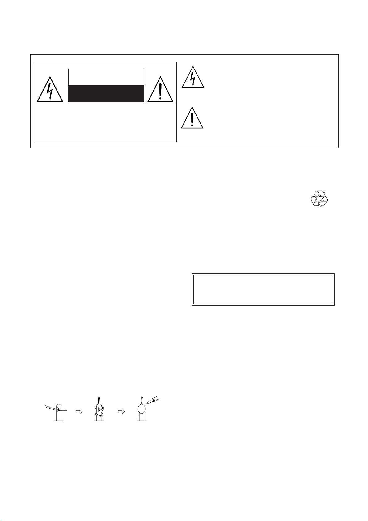
CAUTION
RISK OF ELECTRIC SHOCK
DO NOT OPEN
The lightning flash with arrowhead symbol,
within an equilateral triangle, is intended to
alert the user to the presence of uninsulated
“dangerous voltage” within the product’s enclo
sure that may be of sufficient magnitude to
constitute a risk of electric shock to persons.
CAUTION: TO REDUCE THE RISK OF
ELECTRIC SHOCK, DO NOT REMOVE COVER
(OR BACK). NO USER-SERVICEABLE PARTS
INSIDE. REFER SERVICING TO QUALIFIED
SERVICE PERSONNEL ONLY.
PRECAUTIONS DURING
SERVICING
1. In addition to safety, other parts and
assemblies are specified for conformance with
such regulations as those applying to spurious
radiation. These must also be replaced only
with specified replacements.
Examples: RF converters, tuner units, antenna
selection switches, RF cables, noise-blocking
capacitors, noise-blocking filters, etc.
2. Use specified internal Wiring. Note especially:
1) Wires covered with PVC tubing
2) Double insulated wires
3) High voltage leads
3. Use specified insulating materials for hazardous
live parts. Note especially:
1) Insulating Tape
2) PVC tubing
3) Spacers (insulating barriers)
4) Insulating sheets for transistors
5) Plastic screws for fixing micro switches
4. When replacing AC primary side components
(transformers, power cords, noise blocking
capacitors, etc.), wrap ends of wires securely
about the terminals before soldering.
5. Make sure that wires do not contact heat
generating parts (heat sinks, oxide metal film
resistors, fusible resistors, etc.)
6. Check if replaced wires do not contact sharply
edged or pointed parts.
7. Make sure that foreign objects (screws, solder
droplets, etc.) do not remain inside the set.
The exclamation point within an equilateral
triangle is intended to alert the user to the
presence of important operating and
maintenance (servicing) instructions in the
literature accompanying the appliance.
MAKE YOUR CONTRIBUTION
TO PROTECT THE
ENVIRONMENT
Used batteries with the ISO symbol
for recycling as well as small accumulators
(rechargeable batteries), mini-batteries (cells) and
starter batteries should not be thrown into the
garbage can.
Please leave them at an appropriate depot.
WARNING:
Before servicing this TV receiver, read the
SAFETY INSTRUCTION and PRODUCT
SAFETY NOTICE.
SAFETY INSTRUCTION
The service should not be attempted by anyone
unfamiliar with the necessary instructions on this
apparatus. The following are the necessary
instructions to be observed before servicing.
1. An isolation transformer should be connected in
the power line between the receiver and the
AC line when a service is performed on the
primary of the converter transformer of the set.
2. Comply with all caution and safety related
provided on the back of the cabinet, inside the
cabinet, on the chassis or picture tube.
3. To avoid a shock hazard, always discharge the
picture tube's anode to the chassis ground
before removing the anode cap.
4. Completely discharge the high potential voltage
of the picture tube before handling. The picture
tube is a vacuum and if broken, the glass will
explode.
Page 4
5. When replacing a MAIN PCB in the cabinet,
2/101
always be certain that all protective are
installed properly such as control knobs,
adjustment covers or shields, barriers, isolation
resistor networks etc.
6. When servicing is required, observe the original
lead dressing. Extra precaution should be given
to assure correct lead dressing in the high
voltage area.
7. Keep wires away from high voltage or high
tempera ture components.
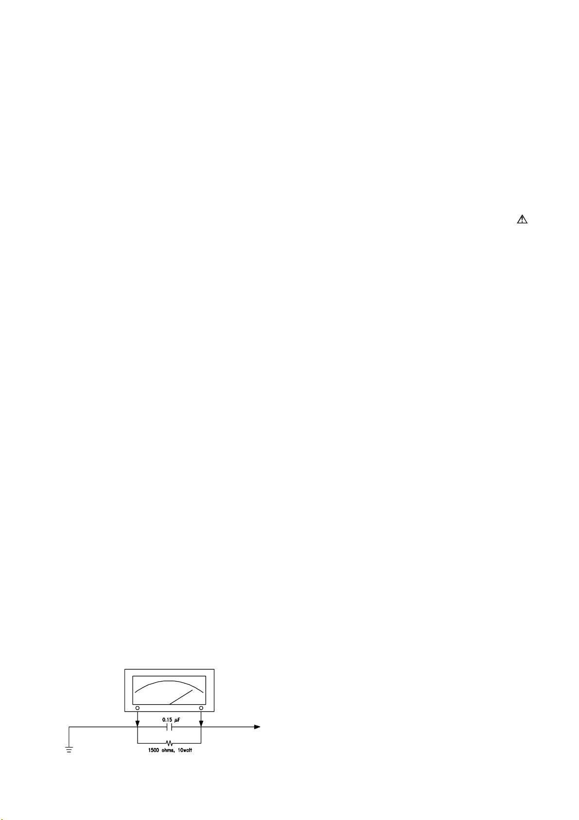
8. Before returning the set to the customer,
always perform an AC leakage current check
on the exposed metallic parts of the cabinet,
such as antennas, terminals, screwheads,metal
overlay, control shafts, etc., to be sure the set
is safe to operate without danger of electrical
shock. Plug the AC line cord directly to the
AC outlet (do not use a line isolation
transformer during this check). Use an AC
voltmeter having 5K ohms volt sensitivity or
more in the following manner.
Connect a 1.5K ohm 10 watt resistor paralleled
by a 0.15µF AC type capacitor, between a
good earth ground (water pipe, conductor etc.,)
and the exposed metallic parts, one at a time.
Measure the AC voltage across the combination
of the 1.5K ohm resistor and 0.15 uF
capacitor. Reverse the AC plug at the AC
outlet and repeat the AC voltage measurements
for each exposed metallic part.
The measured voltage must not exceed 0.3V
RMS.
This corresponds to 0.5mA AC. Any value
exceeding this limit constitutes a potential
shock hazard and must be corrected
immediately.
The resistance measurement should be done
between accessible exposed metal parts and
power cord plug prongs with the power switch
"ON". The resistance should be more than
6M ohms.
AC VOLTMETER
PRODUCT SAFETY NOTICE
Many electrical and mechanical parts in this
apparatus have special safety-related
characteristics.
These characteristics are offer passed
unnoticed by visual spection and the protection
afforded by them cannot necessarily be obtained
by using replacement components rates for a
higher voltage, wattage, etc.
The replacement parts which have these
special safety characteristics are identified by
marks on the schematic diagram and on the parts
list.
Before replacing any of these components,
read the parts list in this manual carefully. The
use of substitute replacement parts which do not
have the same safety characteristics as specified
in the parts list may create shock, fire, or other
hazards.
9. Must be sure that the ground wire of the AC
inlet is connected with the ground of the
apparatus properly.
Good earth ground
such as the water
pipe, conductor,
etc.
AC Leakage Current Check
Place this probe
on each exposed
metallic part
Page 5

3/101
Technical Specifications
PDP4206EM1
1. Standard Test Conditions
All tests shall be performed under the following conditions, unless otherwise specified.
1.1 Ambient light : 150ux (When measuring IB, the ambient luminance
≦0.1Cd/m2)
1.2 Viewing distance : 50cm in front of PDP
1.3 Warm up time : 30 minutes
1.4 PDP Panel facing : no restricted
1.5 Measuring Equipment : PC, Chroma 2225 signal generator (with Chroma digital
additional card) or equivalent, Minolta CA100 photometer
1.6 Magnetic field
: no restricted
1.7 Control settings : Brightness, Contrast, Tint, Color set at Center(50)
1.8 Power input : 100~120Vac 60Hz
1.9 Ambient temperature : 20°C ± 5°C (68°F ± 9°F)
1.10 Display mode : Resolution 852 (H) x 480 (V) Pixels
1.11 Other conditions :
1.11.1 With image sticking protection of PDP module, the luminance will descend
by time on a same still screen and rapidly go down in 5 minutes. When
measuring the color tracking and luminance of a same still screen, be sure t
o accomplish the measurement in one minute to ensure its accuracy.
1.11.2 Due to the structure of PDP, the extra-high-bright same screen should not
hold over 5 minutes for fear of branding on the panel.
Page 6

4/101
Technical Specifications
PDP4206EM1
ELECTRICAL CHARACTERISTICS
2. Power Input
2.1 Voltage : 100 ~120VAC 60Hz
2.2 Input Current : 5.0 /2.5A
2.3 Maximum Inrush Current : <30 A (FOR AC110V ONLY)
Test condition : Measured when switched off for at least 20 mins
2.4 Frequency : 60Hz(±3Hz)
2.5 Power Consumption : 330W Typical
Test condition : full white display with maximum brightness and
contrast
2.6 Power Factor : Meets IEC1000-3-2
2.7 Withstanding voltage : 1.5kVac or 2.2kVdc for 1 sec
3. Display
3.1 Screen Size : 42” Plasma display
3.2 Aspect Ratio : 16:9
3.3 Pixel Resolution : 852x480
3.4 Peak Brightness : 1500 cd/m² (Typical, Panel only)
3.5 Contrast Ratio (Dark room) : 10000:1 (Ratio, Typical, in a dark room, Panel only)
3.6 Viewing Angle : Over 160°
3.7 OSD language : English,French,Spanish.
4. Signal
4.1 AV & Graphic input
4.1.1 Composite signal : AV
4.1.2 Y,C Signal : S-Video
4.1.3 Component signal : YPbPr, HDMI,VGA compatible
4.1.4 Graphic I/P : Analog: D-sub 15pin detachable cable
Digital:HDMI
4.1.5EDID compatibility : DDC 1.3
4.1.6 I/P frequency : f
: 31.5kHz to 60kHz/fV: 56.25Hz to 75Hz(1024x768
H
recommended)
Page 7

5/101
Technical Specifications
4.2 Audio input VGA(D-Sub 15 Pin Type) ×1
PDP4206EM1
D-Sub 9 Pin (RS-232 Input) × 1
HDMI (Ver. 1.1) connector × 1
S-Video (Mini Din 4 Pin) × 1
Video Input (RCA Type) × 1
YPbPr x 2
Stereo, Audio × 6
4.3 Audio output Audio&Video Output (RCA Type) × 1, SPDIF(Optical) x 1
PIP/PBP, Picture size, Picture Still, Sound mode,Last
memory, Timer
5. Environment
5.1 Operating environment
5.1.1 Temperature : 5º to 33°C
5.1.2 Relative humidity: 20% to 85%(non-condensing)
5.2 Storage and Transport
5.2.1 Temperature : -20°C to 60°C(-4º to 140°F)
5.2.2 Relative humidity: 5% to 95%
6. Panel Characteristics
6.1 Type : SDI V4
6.2 Size : 42”,932.94mm(W)X532.80mm(H)
(W/Ostand)
6.3 Aspect ratio : 16:9
6.4 Viewing angle : Over 160°
6.5 Resolution : 852X480
6.6 Weight : 33.6kg ±0.5 kg (Net)w/o stand
6.7 Color : 16.7 millions of colors (R/G/B each 256 scales)
6.8 Contrast : Average 60:1 (In a bright room with 150Lux at center)
Typical 10000:1 (In a dark room 1/100 White Window
pattern at center).
6.9 Peak brightness : Typical 1500cd/㎡ (1/25 White Window)
6.10 Color Coordinate Uniformity : Contrast; Brightness and Color control at normal
setting
Test Pattern : Full white pattern
Average of point A,B,C,D and E +/- 0.01
Page 8

6/101
Technical Specifications
PDP4206EM1
6.11 Color temperature : Contrast at center (50); Brightness center (50);
Color temperature set at Natural
x=0.285±0.02
y=0.290±0.02
6.12 Cell Defect Specifications
Subject to Panel supplier specification as appends.
7. Front Panel Control Button
7.1 SEL. Up / Down Button : Select the Up/Down item in OSD menu.
VOL. Left/Right Button : Push the key to increase the volume left or right.
When selecting the adjusting item in OSD menu
increase or decrease the data-bar.
MENU Button : Display or Exit the OSD menu.
SOURCE Button : Press this button and use up/down button to sellect
the signal sources. AV, S-Video, YPbPr 1,YPbPr 2,
VGA or HDMI.
7.2 STANDBY Button : Switch on main power, or switch off to enter power
Saving modes.
7.3 Main Power Switch : Turn on or off the unit.
8. OSD Function
8.1 Picture : Brightness; Contrast; Saturation; Peaking; Phase; Sharpness; Frequency;
Picture Mode (Normal, Bright, Cinema, User);
Color Temp (Warm, Normal, Cool); etc.
8.2 Window : Image Size (Fill All, Force 4:3, Letter Box, Wide, Anamorphic, etc);
H Position; V Position; H Resolution; Freeze Window (Off, On)
8.3 Audio : Balance; Audio Mode (BBE, Cinema, Music, News, User)
Speaker (Internal, External); AVC (Off, On)
Equalizer (120Hz, 500Hz, 1.2kHz, 3kHz, 12kHz)
8.4 Options : Osd Timeout (5 Sec, 15 Sec, 60 Sec); Menu Background (Opaque,
Translucent); Language(English, French, Spanish); Default Setting;
Close Caption Mode; Close Caption; Content Blocking; Timer
8.5 Layout : Full Screen; PIP; Split Screen
Page 9
Technical Specifications PDP4206EM1
7/101
9. Agency Approvals
Safety : UL, FCC, FDA
Emissions : UL, FCC, FDA
10. Reliability
MTBF : 20,000 hours(Use moving picture signal at 25°C ambient)
11. Accessories
User manual x1, Remote control x1, Stand x 1, Battery x 2, AC Cable x 1
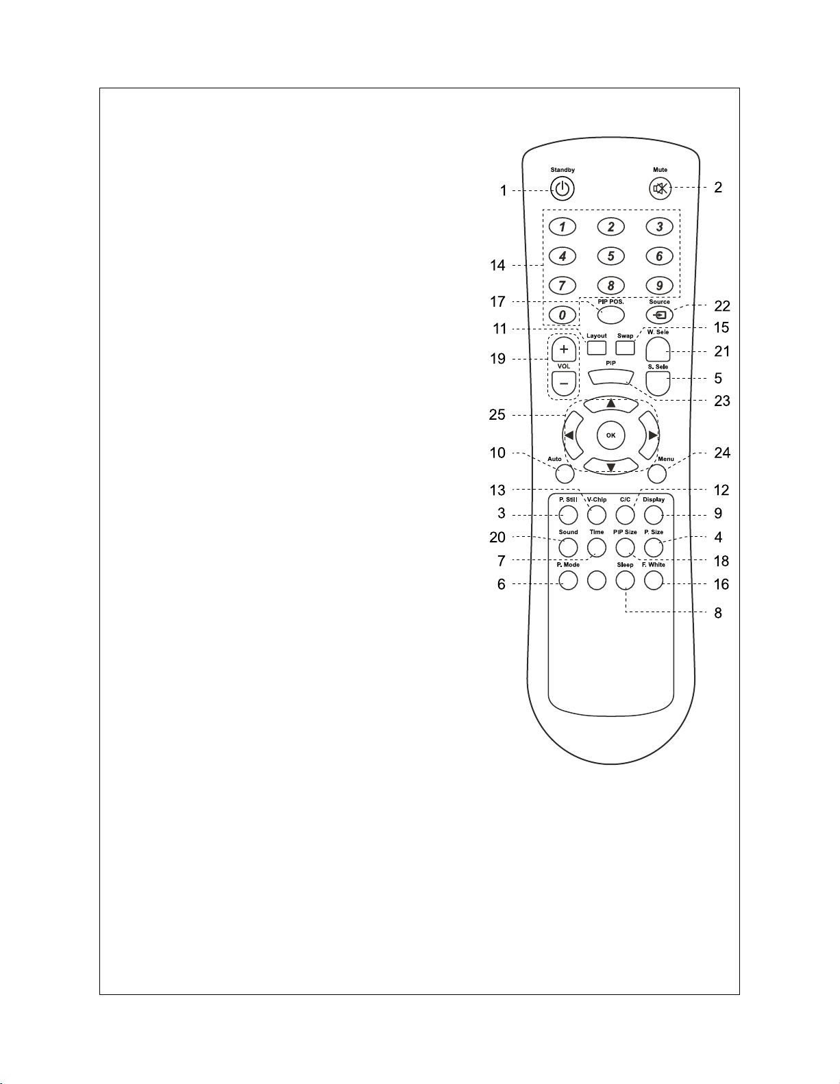
12. Remote Control
1
Standby( ): Press this button to turn off to
standby and turn on from standby.
2 Mute(
system. Press again to reactivate the
sound system.
3 P. Still: Press this button to hold on the
screen. Press again to normal.
4 P. Size: When the input source is
YPbPr 2, VGA or HDMI, press this button,
the picture will change according to Fill All,
Force 4:3, Letter Box, Wide or Anamorphic.
When the input source is AV or S-Video, press
this button, the picture will change according to
Fill All, 4:3, Letter Box, Wide or Anamorphic.
S. Sele: Press this button to select the sound
5
output from Main Window or Sub Window.
6 P. Mode : Press the button to select different
picture effect.
7 Time:
Set” menu.
Sleep: Press this button to
8
time.
Display: Press the button to display the
9
source information.
10 Auto: The Display automatically adjusts the
phase, vertical / horizontal position when
pressing this button in VGA mode.
11 La
menu.
12 C/C: Press this button to enter the Closed
Caption Function. (Only for AV or S-Video)
): Press this button to quiet the sound
YPbPr 1,
Press this button to pop up the “Clock
select
the sleep
yout: Press this button to pop up Layout
(Continued on next page)
Page 10
Technical Specifications PDP4206EM1
8/101
13 V-Chip: Press this button to enter the V-Chip
Function. (Only for AV or S-Video)
14 Number buttons: Use these buttons to enter
the password.
15 Swap: Press this button to switch the Main
window or Sub window pictures in
plit Screen.
S
16 F. White: Press this button to show a full
white picture.
17
PIP POS. : Press the button to select different
Image Position in PIP Mode.
18 PIP Size : Press the button to select different
Image Size in PIP Mode.
19 VOL +/- : Press these buttons to
decrease the volume
20 Sound: Press the button to select different
sound effect.
21
W. Sele: Press this button to select the Main
Window or Sub Window.
22 Source: Press this button and use ▲ / ▼
button to select the signal sources. AV, S-Video,
YPbPr 1, YPbPr 2, VGA or HDMI.
23 PIP: Press this button to change different
Picture Mode.
24
Menu: Press this button to pop up the OSD
Menu and press it again to exit the OSD Menu.
25 OK : Press to enter or confirm.
◄ /
the OSD Menu screen.
▲
the OSD Menu screen.
the screen, but only for the Model with Tuner.
► : They are used as ◄ / ► buttons in
/ ▼ : They are used as ▲ / ▼ buttons in
They also can be used for the selection of the
program when the OSD Menu is not shown on
.
PIP and
increase or
Page 11
Technical Specifications PDP4206EM1
9/101
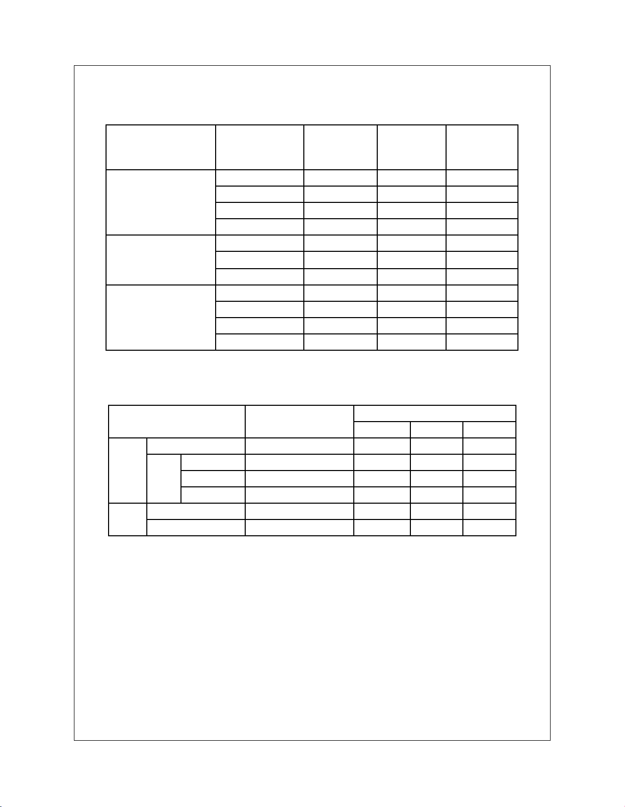
13. Support the Signal Mode
13.1. VGA Mode, HDMI Mode or HDTV Mode (YPbPr 1 or YPbPr 2)
Mode Resolution
VGA Mode
HDMI Mode
HDTV Mode
(YPbPr1/YPbPr2)
13.2.PIP/PBP Screen Mode
Items VGA (Max.)
Main 1024 x 768 OK OK OK
Large 1024 x 768 OK OK OK
PIP
Sub
Middle 1024 x 768 OK OK
Small 1024 x 768 OK OK
Main 1024 x 768 OK OK OK
PBP
Sub 1024 x 768 OK OK OK
Horizontal
Frequency
(kHz)
Vertical
Frequency
(Hz)
Dot Clock
Frequency
(MHz)
640 x 480 31.50 60.00 25.18
800 x 600 37.90 60.32 40.00
1024 x 768 48.40 60.00 65.00
1280 x 1024 64.00 60.01 108.00
1080i 33.75 60.00 74.25
720p 45.00 60.00 74.25
480p 31.468 59.94 27.00
1080i 33.75 60.00 74.25
720p 45.00 60.00 74.25
480p 31.468 59.94 27.00
480i 15.734 59.94 13.50
HDMI/YPbPr1/YPbPr2
480p
720p 1080i
X
X
Note:
- “X” means out of range (can not show).
- When the signal received by the Display exceeds the allowed range, a warning
message shall appear on the screen.
- You can confirm the input signal format from the on-screen.
- VGA 1280 x 1024 Mode don’t recommend working in PIP/PBP Screen Mode.
Page 12

Technical Specifications
10/101
PHYSICAL CHARACTERISTICS
14. Power Cord
Length : 1.8m nominal
Type : optional
15. Cabinet
15.1 Color : black colour as defined by colour plaque reference number
15.2 Weight(W/Ostand)
Net weight : 33.6kg
PDP4206EM1
15.3 Dimensions (W/O stand&speaker)
Width : 1050mm
Height : 657mm
Depth : 99.5mm
Page 13
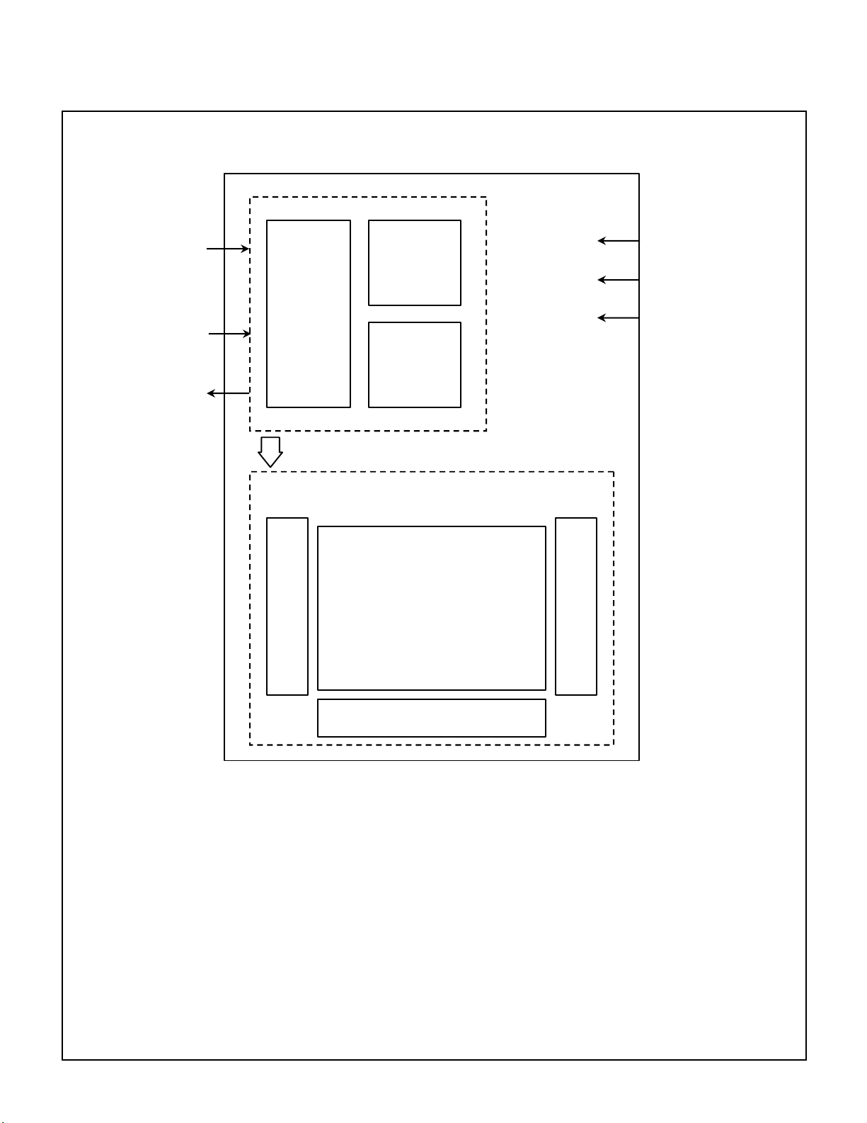
Block Diagram
11/101
Product Specification of PDP Module
LVDS Input
Control Signal
(Serial Interface)
APL Data
Memory
Input
Controller
Interface
Controller
Driver
Timing
Controller
Display data, Driver timing
Color Plasma Display Panel
852 X 480 pixels
Scan Driver
Vs(180V~190V)
Va(55V~65V)
Vcc(+5V)
Common sustain driver
Address Driver
☞ Applied Voltage level is specified at the time when Full-White pattern is displayed on the panel.
Page 14
MAIN/AUDIO BOARDBlock Diagram
12/101
S
C 4344
Audio DAC
3
Page 15

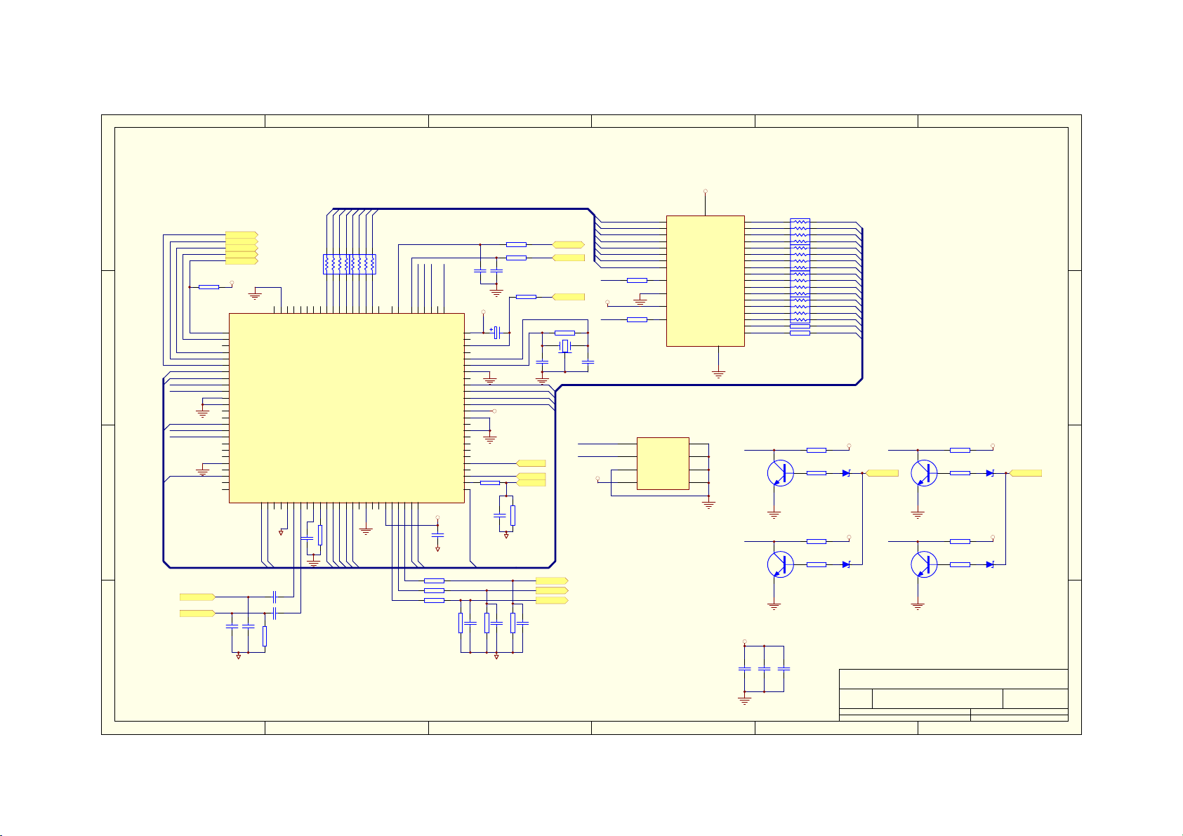
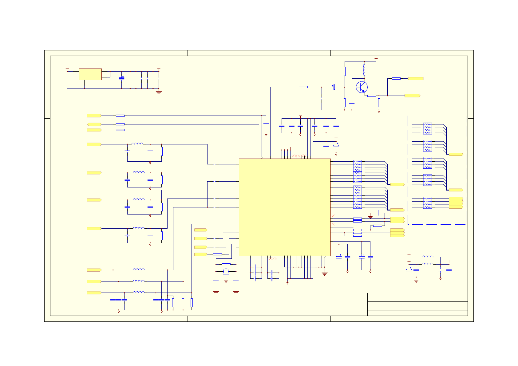
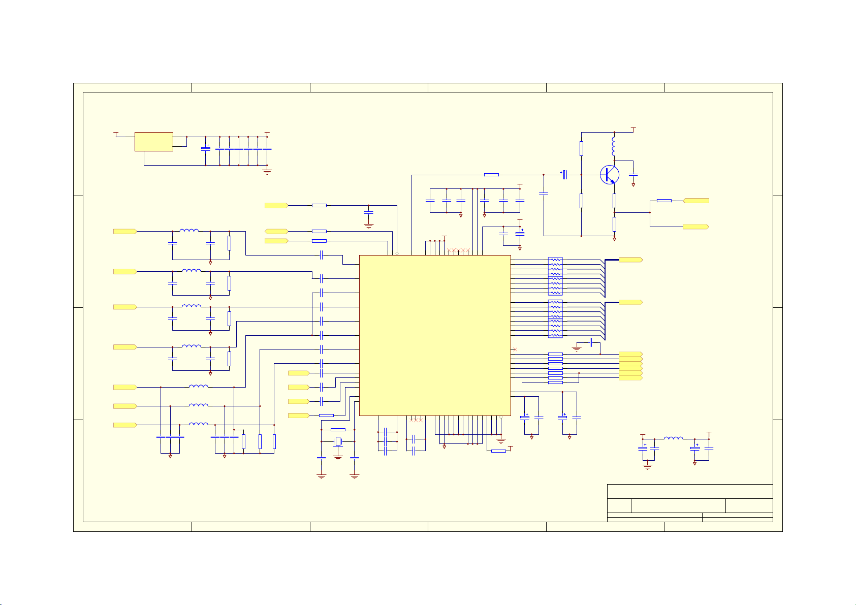
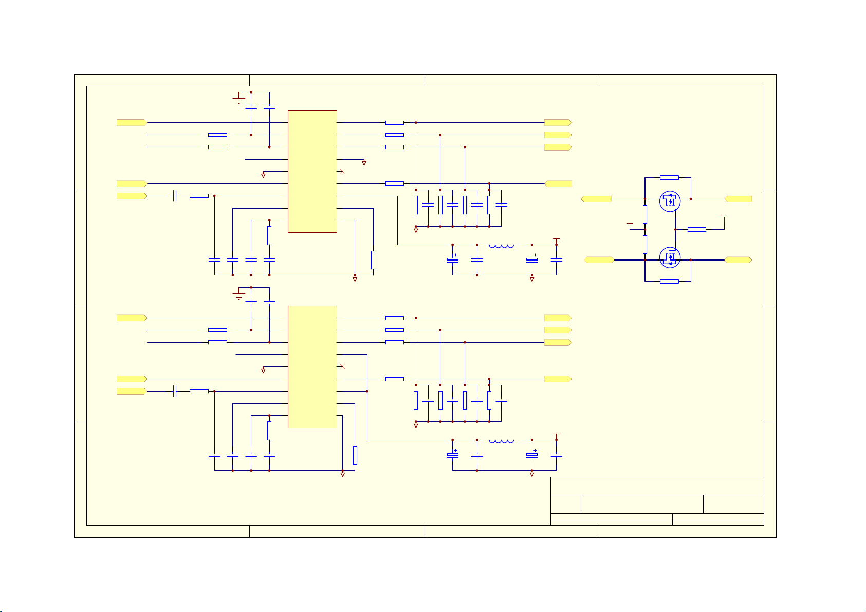
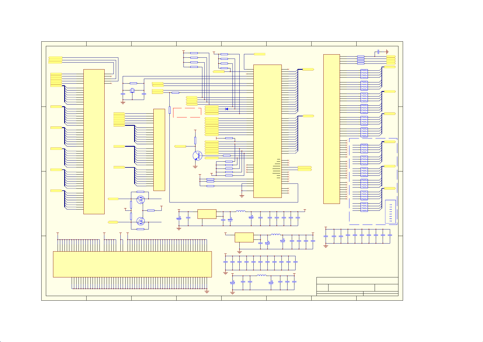
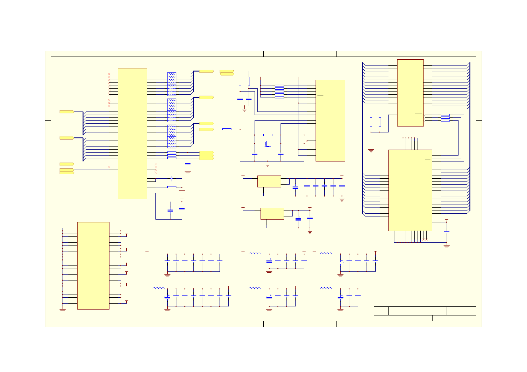
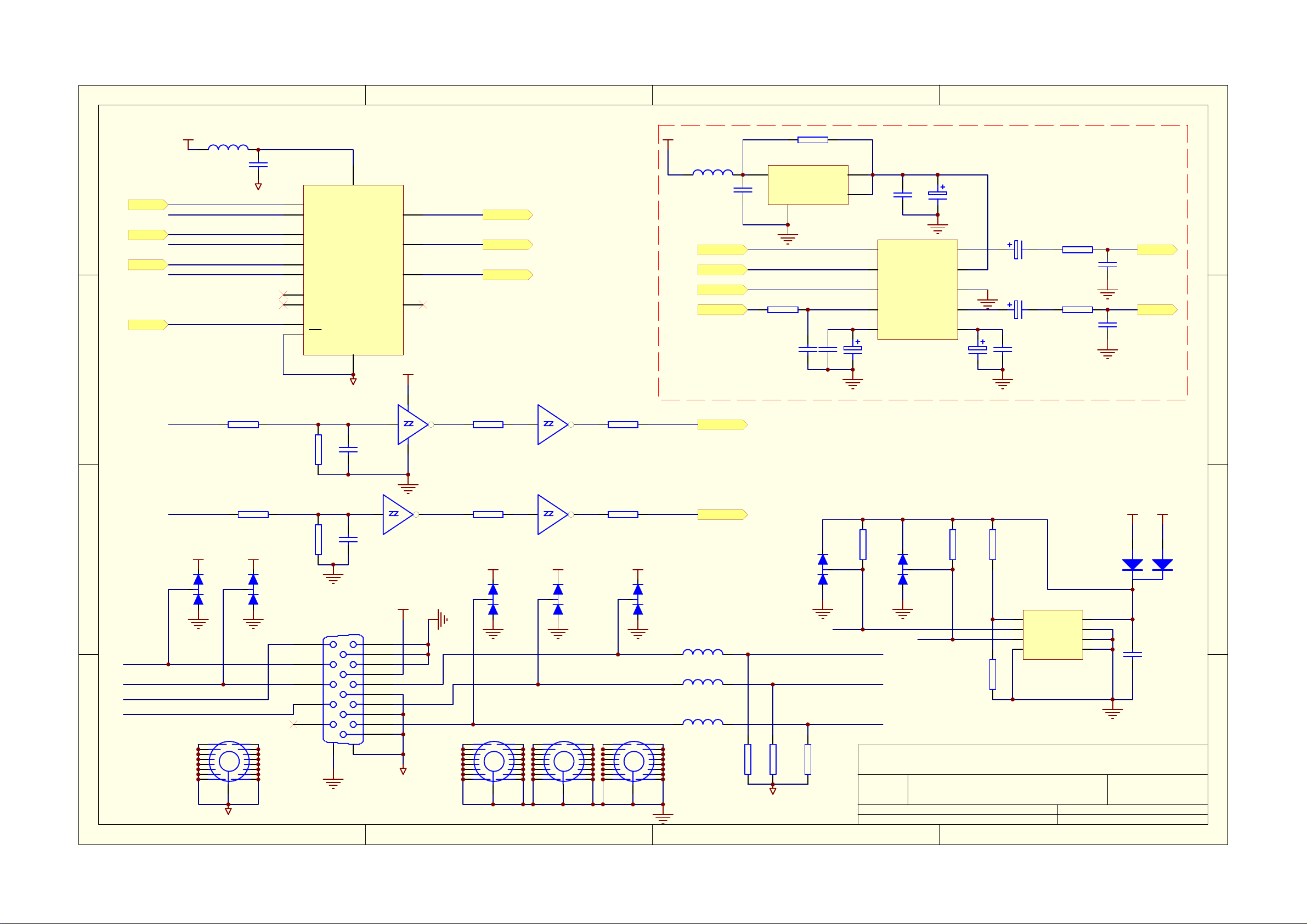
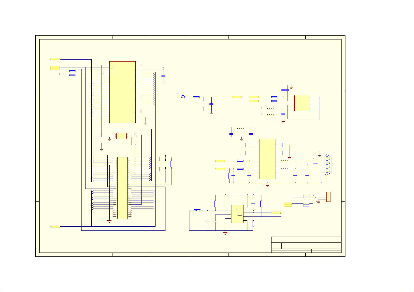
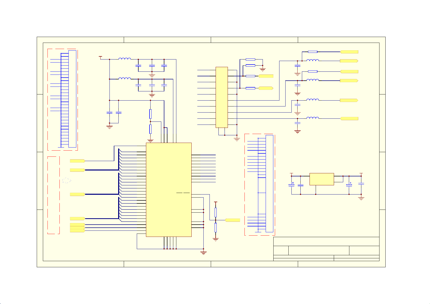
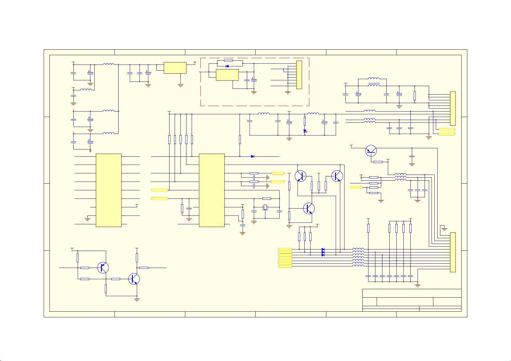
Circuit Diagram
13/101
- Power supply board of Audio Amplifier, MPT012A
- Main (Video) board
- Audio/Tuner board
- Keypad board
- Remote control receiver board
- Remote control board
Page 16
14/101
Page 17
15/101
Page 18
16/101
Page 19
54321
W
17/101
JP902
C954
R929
RP908
OVDD3.3V
1 2
B
1
VIN
2
VCC
3
GND
DDC_SCL3
R921
TVDD3.3V
R922
DDC_SDA3
GRE7
GRE6
GRE5
GRE4
GRE3
GRE2
GRE1
GRE0
GGE7
GGE6
GGE5
GGE4
GGE3
GGE2
GGE1
GGE0
GBE7
GBE6
GBE5
GBE4
GBE3
GBE2
GBE1
GBE0
GPEN
GFBK
GHS
GVS
FIELD
GCLK
GSOG
I2S_MCLK
I2S_SCLK
I2S_LRCLK
I2S_DATA
C955
U907A
7 14
R932
9-HDMI-R
Number RevisionSize
Using digital interface:
DVdd (1.8V) (DVdd+CVdd) 130mA 234mW
PVd (1.8V) (PVd+ALV dd) 30mA 54mW
Vd (3.3V) (Avdd+TVdd) 80mA 264mW
Vdd (3.3V) (Ovdd) 10-120mA, 30mA typical
99mW
Using analog interface:
DVdd 60mA 108mW
PVd 20mA 36mW
Vd 270mA 891m
GRE[7..0]
GGE[7..0]
GBE[7..0]
GPEN
GFBK
FIELD
GCLK
GSOG
I2S_MCLK
I2S_SCLK
I2S_LRCLK
I2S_DATA
R937
R936
R935
3 4
U907B
R923
R924
SPDIFOUT
SD
Q901
G
R925
G
Q902
SD
RP905
RP906
RP903
RP904
RP901
RP902
RP907
R918
R917
R916
R930
Title
Date: 21-Jan-2006 Sheet of
File: F:\4238\PC_B\4238.DDB Drawn By:
5V
C910
D
5V
C912
D3V3B
C914
C
D901 D902
JP901
B
CEC/GND
T120T221T322T4
A
U902
3
INPUT
OUTPUT
GND
1
U903
3
INPUT
OUTPUT
GND
1
U904
3
INPUT
OUTPUT
GND
1
DDC5V DDC5V
DATA2+
DATA2S
DATA2DATA1+
DATA1S
DATA1DATA0+
DATA0S
DATA0-
CLK+
CLKS
HPDET
1
2
3
4
5
6
7
8
9
10
11
12
CLK-
13
CEC
14
NC
15
SCL
16
SDA
17
18
+5V
19
L913
C930
23
D903
D904
D905
D906
D907
D908
D909
D910
1 2 3 4 56
TAB
TAB
TAB
2
4
C901
2
4
C902
2
4
C903
DDC_SCL5
DDC_SDA5
C947C948
HDMI_D2+
HDMI_D2-
HDMI_D1+
HDMI_D1-
HDMI_D0+
HDMI_D0-
HDMI_CK+
HDMI_CK-
DDC_SCL5
DDC_SDA5
HDMI_5V
OVDD3.3V# OVDD3.3V#
C911
SGND
AVDD3.3V#
C913
HDMI-1.8V
C915
R903
R947
U905
7
VCLK
SCL
SDA
GND
R915
HPD_DET
VCC
NC1
NC2
NC3
2
D911
1
6
5
4
HDMI_D0+
HDMI_D0HDMI_D1+
HDMI_D1HDMI_D2+
HDMI_D2HDMI_CK+
HDMI_CK-
8
1
2
3
DDC5V5V
HPD_DET
L900
L901
L902
DDC5V
C929
3
SGND
C904
C905
C906
R941
R942
R943
R944
R945
R946
C922
SCL_H5V
SDA_H5V
GCOAST
HD1_R/Pr
HD1_G/Y
HD1_B/Pb
VGA_VS
VGA_HS
GYCbCr_Cr
GYCbCr_Y
GYCbCr_Cb
C917C916
CVDD1.8V
C920C919
DVDD1.8V
C923
HD1_R/Pr
HD1_G/Y
HD1_B/Pb
GYCbCr_Cr
GYCbCr_Y
GYCbCr_Cb
PLL1.8V
C918
C921
R909
R910
HD1_R/Pr
HD1_G/Y
HD1_B/Pb
GYCbCr_Cr
GYCbCr_Y
GYCbCr_Cb
R912
R913
R908
C939
C940
C941
C942
C945
PLL1.8V
R905
R906
C943
7
6
5
4
L904
C935
C936
C944
C946
DDC_SCL3
DDC_SDA3
HDCP_SCL
HDCP_SDA
SDA#SO
SCL#SO
VCLK
SCL
SDA
GND
L903
C907
C908
C938
HD2_Cr
HD2_Y
HD2_Cb
RP909
VCC
NC1
NC2
NC3
U906
R904
HDMI_D0HDMI_D0+
HDMI_D1HDMI_D1+
HDMI_D2HDMI_D2+
HDMI_CK+
HDMI_CK-
8
1
2
3
C924
C926
57
82
83
C937
46
R907
62
79
74
73
68
61
64
77
71
70
66
60
63
34
35
37
38
40
41
43
44
49
50
51
52
TVDD3.3V
C934
TVDD3.3V
C925
C956
OVDD3.3V
C927 C928
FILT
SCL
SDA
RTERM
COAST/EXTCK
RAIN0
GAIN0
SOG0
BAIN0
VS0
HS0
RAIN1
GAIN1
SOG1
BAIN1
VS1
HS1
RX0RX0+
RX1RX1+
RX2RX2+
RXC+
RXC-
DDC_SCL
DDC_SDA
MCL
MDA
AVDD3.3V#
10
90
100
OVDD1
OVDD2
OVDD3
OGND1
OGND2
OGND3
1
11
91
L914
33
45
TVDD1
DGND1
29
C909
32
TVDD2
CGND1
31
47
48
CVDD1
CVDD2
U901
CGND2
36
30
DVDD
TGND1
TGND2
39
42
AVDD3.3V
C950C949 C951 C952
PLL1.8VDVDD1.8VCVDD1.8V
54
ALVDD
TGND3
ALGND
53
59
56
PVDD1
PGND1
55
58
67
PVDD2
PGND2
AGND1
69
65
SGND
72
76
AVDD1
AVDD2
VSOUT/A0
MCLKOUT
AGND2
AGND3
75
78
80
AVDD3
AVDD4
HSOUT
SOGOUT
FIELD
DCLK
S/PDIF
MCLKIN
SCLK
LRCLK
PWRDN
AGND4
DE
I2S0
I2S1
I2S2
I2S3
R7
R6
R5
R4
R3
R2
R1
R0
G7
G6
G5
G4
G3
G2
G1
G0
B7
B6
B5
B4
B3
B2
B1
B0
DDC_SCL5
DDC_SDA5
92
93
94
95
96
97
98
99
2
3
4
5
6
7
8
9
12
13
14
15
16
17
18
19
88
87
86
85
84
89
28
20
21
22
23
27
26
25
24
81
DDC_SCL5
DDC_SDA5
L915
DDC5V
5V
R919
R920
ADCR7
ADCR6
ADCR5
ADCR4
ADCR3
ADCR2
ADCR1
ADCR0
ADCG7
ADCG6
ADCG5
ADCG4
ADCG3
ADCG2
ADCG1
ADCG0
ADCB7
ADCB6
ADCB5
ADCB4
ADCB3
ADCB2
ADCB1
ADCB0
ADC_DE
ADC_HS
ADC_SOG
ADC_VS
ADC_FIELD
ADC_DCLK
S/PDIF
AVDD3.3V
R914
JP903
3
2
1
GHS
GVS
R933
SCLK
DATA/R
LRCK/L
R938
R928
R927
R926
6
SPDIFOUT
C953R931 R934
C2
V2
Y2
DATA/R
LRCK/L
D
C
B
A
Page 20
54321
18/101
6
D
D3V3D
75
74
73
72
71
70
69
68
67
66
65
64
63
62
61
60
59
58
57
56
55
54
53
52
51
A16_SRAM
C1512
R1528
C1519
C1511
C1513
XTALOUT
XTALIN
A8_SRAM
A9_SRAM
A10_SRAM
A11_SRAM
D3V3D
SGND
R1514
R1515
R1513
TT_VVVS
TT_VVHS
TT_FSO
R1529
SDA_S3V
SCL_S3V
R1505
TT_R
TT_G
TT_B
SDA_S3V
SCL_S3V
3450_rest
/WR_SRAM
D3V3D
/RD_SRAM
X1501
C1505C1504
SDA_NVRAM
SCL_NVRAM
D3V3D
GPIO_P33
GPIO_P32
GPIO_P31
GPIO_P30
TT_SEL
R1527
D3V3D
100
99
1
P2.7
2
P3.0
3
A17_LN
A7_SRAM
SCL_NVRAM
SDA_NVRAM
A6_SRAM
4
5
6
7
8
9
10
11
12
13
14
15
16
17
18
19
20
21
22
23
24
25
P3.1
P3.2
P3.3
A15_LN
A14
/RD
/WR
VSSC
VSSP
P0.5
NC
A7
SCL_NVRAM
SDA_NVRAM
P0.2
NC
NC
VPE
P0.3
A6
P0.4
P3.7
C
A15_SRAM
A14_SRAM
/RD_SRAM
/WR_SRAM
B
P2.0
VSSC
A526A427P0.628P0.729VSSA30CVBS031CVBS132A15_BK33SYNC_FILTER34IREF35A1336A1237A338A239A140FRAME41VPE42/COR43P3.444VDDA45B46G47R48A049RAMBK1
SGND
A5_SRAM
A4_SRAM
TV_CVBS_M#
TV_CVBS_S#
C1503
C1502
D7_SRAM
D6_SRAM
D5_SRAM
D4_SRAM
D3_SRAM
D2_SRAM
D1_SRAM
D0_SRAM
RP1502RP1501
SC1_SW0
SC1_SW1
SC2_SW0
92
98
P2.193P2.294P2.395P2.496P2.597P2.6
82
84
P1.483P1.5
AD085AD186AD287AD388AD489AD590AD691AD7
U1501
SC2_SW1
76
80
81
77
P1.0
P1.178P1.279P1.3
SCL
SDA
RAMBANK0
D3V3_TT_A
50
VDDP
A16_LN
RESET
/RESET
XTALOUT
XTALIN
OSCGND
VDDC
VSSC
VSSP
VSYNC
HSYNC
VDS
NC
NC
A8
A9
A10
A11
NC
P3.6
NC
NC
NC
P3.5
C1510
R1501
C1501
CVBS0
CVBS1
A13_SRAM
A12_SRAM
A3_SRAM
A2_SRAM
A1_SRAM
B_OUT
G_OUT
R_OUT
A0_SRAM
R1510
R1511
R1512
A17_SRAM
SGND
D7_SRAM
D6_SRAM
D5_SRAM
D4_SRAM
D3_SRAM
D2_SRAM
D1_SRAM
D0_SRAM
5
6
7
8
R1506
R1507
U1502
U1503
SDA
SCL
WP
VCC
29
28
27
26
25
23
22
21
30
32
C1514
R1502
R1503
R1504
C1516
C1517
C1515
R1521
A
SGND SGND
C1518
1 2 3 4 56
D3V3D
8
GND
9
A17
10
A16
RP1503
7
A15
11
A14
4
A13
12
A12
RP1504
1
A11
31
A10
2
A9
3
A8
RP1505
13
A7
14
A6
15
A5
16
A4
RP1506
17
A3
18
A2
R1508
19
A1
R1509
20
A0
I/O8
I/O7
VCC
I/O6
I/O5
I/O4
I/O3
I/O2
I/O1
5
/WE
/CE1
6
CE2
/OE
A17_SRAM
A16_SRAM
A15_SRAM
A14_SRAM
A13_SRAM
A12_SRAM
A11_SRAM
A10_SRAM
A9_SRAM
A8_SRAM
A7_SRAM
A6_SRAM
A5_SRAM
A4_SRAM
A3_SRAM
A2_SRAM
A1_SRAM
A0_SRAM
24
GND
4
3
NC2
2
NC1
1
NC0
Q1501
Q1503
R1516
R1517
R1522
R1523
D3V3D
D1501
D3V3D
D1503
SC2_SW
SC1_SW0SC1_SW1
Q1502
SC2_SW0SC2_SW1
Q1504
R1519
R1520
R1525
R1526
D3V3D
D1502
D3V3D
D1504
SC1_SW
D3V3D
C1506 C1507 C1508
Title
15_TELETEXT_DECODER
Number RevisionSize
B
Date: 14-Oct-2005 Sheet of
File: F:\4228\4228_temp_ddb\4228_Temp.DDB Drawn By:
D
C
B
A
Page 21
54321
19/101
A5V
U1101
5V
3
INPUT
GND
C1108
D
1
OUTPUT
TAB
2
4
C1105
C1109
C1110
C1111
C1112
C1113
VV33
C1114
CVBS_O
R1114
R1112
C1164
R1113 R1106
C1171
L1112
Q1101 R1104
C1163
R1121
3230_VO
TV_CVBS_M#
3230_VO
6
D
MREST
SDA_S3V
SCL_S3V
V_AVCVBS
C
V_TVCVBS
V_SVideo_C
B
V_SVideo_Y
VYCbCr_Y
VYCbCr_Cb
A
VYCbCr_Cr
1 2 3 4 56
R1103
R1101
R1102
C1160
C1150 C1151
C1128
C1154
C1173
C1172
C1174
SGND
L1111
L1104
L1105
L1106
L1107
L1108
L1102
C1159
C1149
C1156
SGND
SGND
SGND
SGND
C1125
R1117
SGND
R1115
R1116
R1118
C1126
C1127
V_TT_G
V_TT_B
V_TT_R
V_TT_FSO
R1126R1125R1124
R1127
C1116
C1117
C1115
C1118
C1119
C1120
C1121
C1122
C1166
C1167
C1168
R1119
X1101
C1124
70
14
13
74
VIN3
SCL
73
VIN2
75
VIN4
71
CIN
72
VIN1
5
Y2/G2
4
U2/B2
6
V2/R2
2
Y1/G1
1
U1/B1
3
V1/R1
79
FBIN1
62
XTALI
63
XTALO
VDDCAP9GNDCAP
C1132
C1123
C1140
C1131C1130
10
15
SDA
RST#
VOUT
U1102
ADR:0x88
CLK560FPDAT58CLK2024ASGND7ASGND64GND
APGND25APVDD26PLGND30YGND35CGND46SPGND51AFGND65ISGND68ISGND77ISGND80I2CSEL
12
C1133
C1134
5VVV
C1141 C1142 C1143 C1144C1145C1146
SGND
SGND
VV33
23
45
29
VDD
PLVDD
11
SGND
52
YVDD36CVDD
SPVDD
19
FFIE
59
20
21
76
69
FFRE22FFOE
FFWE
FFRST
ISVDD
AFVDD
VSTBY
SGND
5VVV
C1147C1148
RP1101
RP1102
RP1103
SGND
31
Y7
32
Y6
33
Y5
34
Y4
37
Y3
38
Y2
39
Y1
40
Y0
41
UV7
42
UV6
43
UV5
44
UV4
47
UV3
48
UV2
49
UV1
50
UV0
27
LLC2
28
LLC
56
HS
53
INTLC
54
AVO
55
HCLP
57
VS
78
VREF
66
VRT
VGAV
OE#
TEST
C1137 C1135
17
18
16
67
RP1104
R1109
#VPEN
R1107
R1105
R1108
REF_V
C1138 C1136
SGND SGND
VY7
VY6
VY5
VY4
VY3
VY2
VY1
VY0
VY[7..0]
VUV7
VUV6
VUV5
VUV4
VUV3
VUV2
VUV1
VUV0
C1139
VUV[7..0]
VVCLK
VVHS
R1110
R1123
VVVS
Title
B
Date: 14-Oct-2005 Sheet of
File: F:\4228\4228_temp_ddb\4228_Temp.DDB Drawn By:
VVCLK
VVHS
TT_VVHS
VVVS
TT_VVVS
C1103
11-DECODERV
Number RevisionSize
RP1105
L1101
C1106
RP1106
RP1107
RP1108
RP1109
L1103
C1104
VG7
VG6
VG5
VG4
VG3
VG2
VG1
VG0
VB7
VB6
VB5
VB4
VB3
VB2
VB1
VB0
SGND
5VVV
VY7
VY6
VY5
VY4
VY3
VY2
VY1
VY0
VUV7
VUV6
VUV5
VUV4
VUV3
VUV2
VUV1
VUV0
#VPEN
VVVS
VVHS
VVCLK
Install RP1105~RP1109 if cancel deinterlace IC
A5V
5V
C1107
VG[7..0]
VB[7..0]
VPEN
VVS
VHS
VCLK
C
B
A
Page 22
54321
20/101
6
U1401
5V
3
D
C
B
A
INPUT
GND
1
G_AVCVBS
G_AVCVBS
G_TVCVBS
G_SVideo_C
G_SVideo_Y
GYCbCr_Y
GYCbCr_Y
GYCbCr_Cb
GYCbCr_Cb
GYCbCr_Cr
GYCbCr_Cr
1 2 3 4 56
2
OUTPUT
4
TAB
C1405
L1407
C1460 C1459
L1408
C1450 C1451
L1402
C1428 C1449
L1411
C1454 C1456
L1404
L1405
L1406
C1473
C1474
C1472
SGND
SGND
SGND
SGND
SGND
C1425
C1409
SGND
C1410
R1415
R1416
R1418
C1426
R1417
C1427
C1411
C1412
C1413
GV33
C1414
MREST
SDA_S3V
SCL_S3V
R1426R1425R1424
G_TT_G
G_TT_B
G_TT_R
G_TT_FSO
R1403
R1401
R1402
R1427
C1416
C1417
C1415
C1418
C1419
C1420
C1421
C1422
C1466
C1467
C1468
R1419
X1401
C1431C1430
74
73
75
71
72
79
62
63
C1424
5
4
6
2
1
3
VIN3
VIN2
VIN4
CIN
VIN1
Y2/G2
U2/B2
V2/R2
Y1/G1
U1/B1
V1/R1
FBIN1
XTALI
XTALO
C1432
C1423
C1440
CVBS_S_O
14
13
SCL
10
15
70
SDA
RST#
VOUT
U1402
ADR:0x8E
VDDCAP9GNDCAP
CLK560FPDAT58CLK2024ASGND7ASGND64GND
APGND25APVDD26PLGND30YGND35CGND46SPGND51AFGND65ISGND68ISGND77ISGND80I2CSEL
12
C1433
C1434
C1441 C1442 C1443 C1444C1445C1446
SGND
SGND
GV33
19
23
45
21
29
52
69
20
76
FFIE
VDD
PLVDD
YVDD36CVDD
11
SGND
SPVDD
FFWE
FFRST
FFRE22FFOE
ISVDD
AFVDD
R1412
R1414
5VVG
5VVG
59
VSTBY
SGND
31
Y7
32
Y6
33
Y5
34
Y4
37
Y3
38
Y2
39
Y1
40
Y0
41
UV7
42
UV6
43
UV5
44
UV4
47
UV3
48
UV2
49
UV1
50
UV0
27
LLC2
28
LLC
56
HS
53
INTLC
54
AVO
55
HCLP
57
VS
78
VREF
66
VRT
VGAV
OE#
TEST
C1437 C1435
17
18
16
67
5VVG
R1420
C1464
C1471
C1447C1448
RP1401
RP1402
RP1403
RP1404
R1409
R1410
R1408
R1407
R1422
R1405
R1423GHS
REF_G
C1438 C1436
SGND SGND
R1413
C1439
Q1401
GGE7
GGE6
GGE5
GGE4
GGE3
GGE2
GGE1
GGE0
GBE7
GBE6
GBE5
GBE4
GBE3
GBE2
GBE1
GBE0
GHS
TT-GHS
A5V
L1412
C1463
SGND
R1404
R1406
SGND
GGE[7..0]
GBE[7..0]
GCLK
GHS
FIELD
GPEN
TT-GHS
GVS
C1403
Title
14-DECODER_G
B
Date: 14-Oct-2005 Sheet of
File: F:\4228\4228_temp_ddb\4228_Temp.DDB Drawn By:
R1421
TV_CVBS_S#
TV_CVBS_S
TV_CVBS_S
C1404
5VVG
C1407
SGND
5V
L1401
C1406
Number RevisionSize
D
C
B
A
Page 23
321
21/101
4
C860 C861
TT_VVVS
D
TT_VVHS
3230_VO
C
B
TV_CVBS_S
GVS
TT-GHS
SDA_S5V
SCL_S5V
C855
SDA_S5V
SCL_S5V
C809
R857
R803
R855
R856
R801
R802
C856
C810
C857
5V_G_CCD
C811
13
14
15
5V_V_CCD
SGND
R858
C858 C859
C814 C815
13
14
15
SGND
R804
C812 C813
Vin/INTRO
SDA
SCK
4
SEN
6
SMS
5
HIN
7
VIDEO
8
CSYNC
LPF9VSS(A)
Vin/INTRO
SDA
SCK
4
SEN
6
SMS
5
HIN
7
VIDEO
8
CSYNC
LPF9VSS(A)
U803
U802
I2C/SEL
SDO
BOX
VDD
RREF
I2C/SEL
SDO
BOX
VDD
RREF
R
G
B
R
G
B
2
3
1
16
17
12
10
11
SGND
18
2
3
1
16
17
12
10
11
SGND
R805
R861
R862
R863
5V_V_CCD
R859
R806
R807
R808
R809
5V_G_CCD
R864
SGND
R810
SGND
C862
C817
C804
C802
R865
R811
C863
C818
R866
R812
C864
C819
R860
18
C807
C808
R867
L801
R813
L802
C865
C820
V_TT_R
V_TT_G
V_TT_B
V_TT_FSO
C803
G_TT_R
G_TT_G
G_TT_B
G_TT_FSO
C801
SGND
V_TT_R
V_TT_G
V_TT_B
V_TT_FSO
A5V
G_TT_R
G_TT_G
G_TT_B
G_TT_FSO
A5V
C806
C805
SCL_S5V
SDA_S5V
SCL_S5V
SDA_S5V
D
R815
SD
R814
Q801
G
R852
G
Q802
SD
R854
5V
R853
SCL_S3V
V33SW
C
SDA_S3V
B
Title
A
1 2 34
SGND
SGND
8-CCD_DECODER
Number RevisionSize
A4
Date: 14-Oct-2005 Sheet of
File: F:\4228\4228_temp_ddb\4228_Temp.DDB Drawn By:
A
Page 24
7654321
22/101
D3V3B
R1305
GCOAST
GBLKSPL
GFBK
U1301A
A10
GCLK
D
GPEN
GVS
GHS
GSOG
GRE[7..0]
GRE0
GRE1
GRE2
GRE3
GRE4
GRE5
GRE6
GRE7
GGE[7..0]
GGE0
GGE1
GGE2
GGE3
GGE4
GGE5
GGE6
GGE7
GBE[7..0]
GBE0
GBE1
GBE2
GBE3
C
B
A
GBE4
GBE5
GBE6
GBE7
GRO[7..0]
GRO0
GRO1
GRO2
GRO3
GRO4
GRO5
GRO6
GRO7
GGO[7..0]
GGO0
GGO1
GGO2
GGO3
GGO4
GGO5
GGO6
GGO7
GBO[7..0]
GBO0
GBO1
GBO2
GBO3
GBO4
GBO5
GBO6
GBO7
M16
T8
VIO16R6VIO17R7VIO18R8VIO19
1 2 3 4 5 6 78
GCLK
B9
GPEN
A9
GVS
C10
GHS
B10
GSOG
E4
GRE0
C3
GRE1
B1
GRE2
F4
GRE3
C2
GRE4
C1
GRE5
D3
GRE6
D2
GRE7
C11
GGE0
B12
GGE1
B11
GGE2
A8
GGE3
B8
GGE4
C8
GGE5
A7
GGE6
B7
GGE7
B18
GBE0
A20
GBE1
B17
GBE2
A19
GBE3
B16
GBE4
A17
GBE5
A16
GBE6
A15
GBE7
A6
GRO0
C7
GRO1
B6
GRO2
A5
GRO3
D7
GRO4
B5
GRO5
C6
GRO6
A4
GRO7
C13
GGO0
B15
GGO1
A14
GGO2
B14
GGO3
A13
GGO4
C12
GGO5
B13
GGO6
A12
GGO7
C18
GBO0
E17
GBO1
C17
GBO2
B19
GBO3
E16
GBO4
C16
GBO5
C15
GBO6
D14
GBO7
G15
G16
J16
L16
F14
F15
G6
VIO7
VIO8G5VIO9
VIO10
VIO11
VIO12
VIO13
VIO14M5VIO15
GND52
GND53
GND54
GND55
GND56R5GND57
GND58
GND59
Y7
P17
N12
N13
N17
N18
U12
U14
GFBK
GREF
GBLKSPL
GCOAST
GHSFOUT
PW181 Graphics Port
VIO1E6VIO2E8VIO3F5VIO4F6VIO5F7VIO6
GND47N8GND48N9GND49
GND50
GND51
N10
N11
M13
A11
D10
C14
A18
C9
SCL_H5V
SDA_H5V
T16
U11
U13
VCC3U5VCC4U9VCC5
VCC6
GND41M8GND42M9GND43
GND44
GND45
GND46
M10
M11
M12
R1301
X1301
C1301
VCLK
VVS
VHS
FIELD
VPEN
VR[7..0]
VG[7..0]
VB[7..0]
VCC1A2VCC2
PW818 POWER AND GROUND
GND40
L13
L18
SCL_H5V
5Vstby
SDA_H5V
C4
GND38
GND39
L11
L12
C1302
VR0
VR1
VR2
VR3
VR4
VR5
VR6
VR7
VG0
VG1
VG2
VG3
VG4
VG5
VG6
VG7
VB0
VB1
VB2
VB3
VB4
VB5
VB6
VB7
R1334
R1314
R1315
R1335
V15V15pV25D3V3B
T10
T11
T12
T13
T14
T15
VPP1B4VPP2
VDD31
VDD32
VDD33
VDD34
VDD35
GND31
GND32
GND33
GND34L8GND35L9GND36
GND37
L10
K10
K11
K12
K13
RXD
TXD
IR_181
NMI
R1303
R1304
U1301B
E1
VCLK
E3
VVS
F3
VHS
D1
FIELD
N2
VPEN
E2
VR0
F1
VR1
F2
VR2
G3
VR3
G2
VR4
H3
VR5
H2
VR6
G1
VR7
J4
VG0
H1
VG1
J3
VG2
J2
VG3
J1
PW181 Video Port
VG4
K3
VG5
K2
VG6
K1
VG7
L2
VB0
L1
VB1
L3
VB2
L4
VB3
M3
VB4
M1
VB5
N1
VB6
M2
VB7
SD
SCL_H3V
Q1301
D3V3C
G
R1316
G
Q1302
SD
SDA_H3V
R13
R14
R15
VDD25
VDD26
VDD27T6VDD28T7VDD29T9VDD30
GND25
GND26
GND27K4GND28K8GND29K9GND30
J11
J12
J13
C1324
N15
N16
P15
P16
VDD19
VDD20P5VDD21P6VDD22
VDD23
VDD24
GND18
GND19
GND20
GND21J8GND22J9GND23
GND24
J10
H10
H11
H12
H13
R1306
R1307
R1308
SDA_H3V
SCL_H3V
SDA_S3V
SCL_S3V
REMARK:
HARDWARE I2C: SD A1 SCL1
SOFTWARE I2C: VSDA VSCL
D3V3B
MREST
Q1303
5V
3
C1303
H16
K16
E14
E15
F16
VDD8
VDD9
VDD10H5VDD11
VDD12J5VDD13K5VDD14
VDD15L5VDD16N5VDD17N6VDD18
GND9
GND10
GND11
GND12G4GND13
GND14H4GND15H8GND16H9GND17
D11
D12
D13
D15
G17
VDD7
D3V3B
R1329
R1321
R1322
R1323
VGASEL
SDA_H3V
SCL_H3V
GAFEOE
MUTE
SEL1
SEL0
KEY0
KEY1
KEY2
KEY3
KEY4
KEY5
KEY6
SP_RELAY
R1309
D3V3B
COMMUNIC
P_SCLK
P_SDATA
P_SLE
DTXON
HPD_DET
3450_rest
D3V3B
D3V3B
R1311
R1312
R1313
U1302
INPUT
OUTPUT
GND
1
E10
E11
E12
E13
VDD1E7VDD2E9VDD3
VDD4
VDD5
VDD6
GND1A1GND2B2GND3B3GND4D4GND5D5GND6D8GND7D9GND8
D1302
R1333
R1310
R1325
R1332
R1331
R1326
R1324
L1302
2
4
TAB
C1355
C1326
U1303
D3V3B
3
INPUT
1
U1301E
V15
C1333 C1334 C1335 C1336 C1337 C1338 C1339 C1340 C1341 C1342 C1343
V15
12
C1346
C1325
OUTPUT
GND
C1349 C1350
RESET
U1301D
Y11
RESET
E5
MCKEXT
D6
DCKEXT
A3
XI
C5
XO
Y12
RXD
V12
TXD
V11
IRRCVR0
W11
IRRCVR1
V13
PORTA0
W13
PORTA1
Y13
PORTA2
Y14
PORTA3
W14
PORTA4
Y15
PORTA5
W15
PORTA6
V15
PORTA7
R17
PORTB0
W18
PORTB1
V18
PORTB2
Y18
PORTB3
U18
PORTB4
Y19
PORTB5
W19
T18
T17
V16
W16
Y16
V17
U17
W17
Y17
P1
Y2
M4
N3
U16
N4
T5
P2
U15
TAB
PW181 MISC
PORTB6
PORTB7
PORTC0
PORTC1
PORTC2
PORTC3
PORTC4
PORTC5
PORTC6
PORTC7
CPUTMS
CPUTCK
CPUDI
CPUDO
MODE0
MODE1
MODE2
MODE3
ADR24B
RNMI2
C1304 C1305 C1306 C1307 C1308 C1309
2
4
C1357
C1312
L1301
ROMOE
ROMWE
RAMOE
RAMWE
EXTINT
L1304
C1332
BHEN
DNC1
DNC2
DNC3
U4
A0
T4
A1
V3
A2
U3
A3
Y1
A4
W2
A5
T3
A6
V2
A7
U2
A8
W1
A9
R4
A10
V1
A11
P4
A12
R3
A13
T2
A14
U1
A15
T1
A16
R2
A17
R1
A18
P3
A19
V10
D0
Y10
D1
Y9
D2
W9
D3
V9
D4
Y8
D5
W8
D6
V8
D7
W7
D8
U8
D9
V7
D10
W6
D11
Y6
D12
V6
D13
U7
D14
U6
D15
W3
RD
Y3
WR
W12
V5
W4
W5
Y5
Y4
CS1
V4
CS0
U10
W10
NMI
B20
C19
V14
C1344
C1351 C1352 C1353
A1
A2
A3
A4
A5
A6
A7
A8
A9
A10
A11
A12
A13
A14
A15
A16
A17
A18
A19
D0
D1
D2
D3
D4
D5
D6
D7
D8
D9
D10
D11
D12
D13
D14
D15
C1331
V15p
A[19..1]
D[15..0]
ROMOEn
ROMWEn
V25
C1330 C1329 C1328
U1301C
D3V3B
V15
Title
13-SCALER
A3
Date: 14-Oct-2005 Sheet of
File: F:\4228\4228_temp_ddb\4228_Temp.DDBDrawn By:
DCLK
DVS
DHS
DEN
DRE1
DRE5
DRE6
DRE0
DRE7
DRE3
DRE2
DRE4
DGE1
DGE0
DGE3
DGE2
DGE7
DGE6
DGE5
DGE4
DBE0
DBE3
DBE1
DBE2
DBE4
DBE7
DBE6
DBE5
DRO0
DRO1
DRO2
PW181 Display Port
DRO3
DRO4
DRO5
DRO6
DRO7
DGO0
DGO1
DGO2
DGO3
DGO4
DGO5
DGO6
DGO7
DBO0
DBO1
DBO2
DBO3
DBO4
DBO5
DBO6
DBO7
Number RevisionSize
J17
R1317
C20
R1318
D18
R1319
N19
R1320
DR1
Y20
RP1302
DR5
W20
DR6
V20
V19
DR0
DR7
U20
RP1303
DR3
U19
DR2
R16
DR4
R18
DG1
T20
RP1304
DG0
T19
DG3
R20
DG2
R19
DG7
P20
RP1305
DG6
P19
DG5
P18
DG4
M18
DB0
M17
RP1306
DB3
L17
DB1
N20
DB2
M20
DB4
M19
RP1307
DB7
L20
DB6
L19
DB5
K17
K19
K20
DR1
K18
DR5
J20
DR6
J18
J19
DR0
H20
H19
DR7
DR3
DR2
H18
DR4
H17
G20
G19
DG1
G18
DG0
F20
DG3
F19
DG2
F18
DG7
E20
DG6
DG5
E19
E18
DG4
F17
D20
DB0
D19
DB3
DB1
D16
D17
DB2
DB4
DB7
DB6
DB5
For Samsung/Formosa panel
2005.05.22
C1322 C1321 C1320 C1319 C1318 C1317 C1316
C1315C1314C1313
RP1308
RP1309
RP1310
RP1311
RP1312
RP1313
C1354
DRE1
DRE5
DRE6
DRE0
DRE7
DRE3
DRE2
DRE4
DGE1
DGE0
DGE3
DGE2
DGE7
DGE6
DGE5
DGE4
DBE0
DBE3
DBE1
DBE2
DBE4
DBE7
DBE6
DBE5
DRE3
DRE7
DRE0
DRE2
DRE1
DRE5
DRE4
DRE6
DGE3
DGE2
DGE5
DGE4
DGE1
DGE0
DGE7
DGE6
DBE2
DBE5
DBE3
DBE4
DBE6
DBE1
DBE0
DBE7
8
DCLK
DVS
DHS
DEN
DRE[7..0]
D
DGE[7..0]
DBE[7..0]
C
DRE[7..0]
DGE[7..0]
DBE[7..0]
181 LVDS
B
R0
R6
R1
R7
R2
R0
R3
R1
R4
R2
R5
R3
R6
R4
R7
R5
A
Page 25
54321
23/101
40
31RAMA0
U1201A
82
VB0
83
VB1
84
VB2
85
VB3
86
VB4
D
VY[7..0]
VUV[7..0]
C
VVCLK
VVVS
VVHS
VY0
VY1
VY2
VY3
VY4
VY5
VY6
VY7
VUV0
VUV1
VUV2
VUV3
VUV4
VUV5
VUV6
VUV7
87
VB5
88
VB6
89
VB7
92
SVHS
93
SVVS
94
SVCLK
95
VG0
96
VG1
97
VG2
98
VG3
99
VG4
100
VG5
101
VG6
102
VG7
109
VR0
110
VR1
111
VR2
112
VR3
113
VR4
114
115
116
105
106
107
108
PW1231 VIDEO BLOCK
VR5
VR6
VR7
PVCLK
CREF
PVVS
PVHS
DCLK
DVS
DHS
ADSVM
ADR
ADG
VREFIN
VREFOUT
RSET
COMP
ADR:0x64
B
A
8
VSS0
71
VSS1
104
VSS2
134
122
147
123
U1201D
VSS3
1
PVSS0
9
PVSS1
53
PVSS2
79
PVSS3
91
PVSS4
PVSS5
PVSS6
78
DPAVSS
76
DPDVSS
MPAVSS
11
29
32
17
20
23
14
PW1231 POWER AND GROUND
ADDVSS
ADAVSS
ADGVSS
AVS33B
AVS33G
AVS33R
AVS33SVM
AVD33SVM
1 2 3 4 56
VDD0
VDD1
VDD2
VDD3
PVDD0
PVDD1
PVDD2
PVDD3
PVDD4
PVDD5
PVDD6
DPAVDD
DPDVDD
MPAVDD
ADDVDD
ADAVDD
ADGVDD
AVD33B
AVD33G
AVD33R
7
70
V25SW
103
133
30
52
V33SW1
80
90
121
146
160
AV25p1
77
75
AV25p2
124
10
AV25a
28
31
16
19
22
AV331
13
DR0
DR1
DR2
DR3
DR4
DR5
DR6
DR7
DG0
DG1
DG2
DG3
DG4
DG5
DG6
DG7
DB0
DB1
DB2
DB3
DB4
DB5
DB6
DB7
ADB
V33SW
RP1201
157
158
159
2
RP1202
3
4
5
6
RP1203
149
150
151
152
RP1204
153
154
155
156
RP1205
139
140
141
142
RP1206
143
144
145
148
R1212
136
R1211
137
R1213
138
12
21
18
15
C1203
26
27
R1214
24
25
C1243
C1247
AV331
C1211
C1210 C1212 C1213 C1214 C1215 C1216 C1217
C1227 C1228 C1229 C1230 C1231 C1232 C1233
VR[7..0]
VR0
VR1
VR2
VR3
VR4
VR5
VR6
VR7
VG[7..0]
VG0
VG1
VG2
VG3
VG4
VG5
VG6
VG7
VB[7..0]
VB0
VB1
MREST
VB2
VB3
VB4
VB5
VB6
VB7
VCLK
VVS
VHS
C1251
SCL_S3V
SDA_S3V
R1203
V33SW1V33SW
V33SW
R1202R1201
R1204
R1205
R1206
L1201
L1204L1203
R1207
R1208
R1215
X1201
U1202
3
INPUT
OUTPUT
TAB
GND
1
U1204
3
INPUT
OUTPUT
GND
1
C1249
C1248
C1201 C1202
C1244
5V V25SW
5V
V25SW
V25SW
V33SW
C1218C1241
2
C1242
4
2
C1245
4
TAB
AV25A
C1219 C1220 C1221 C1223
AV25P1
C1234 C1235 C1236
127
128
129
130
131
119
120
125
126
117
118
132
73
72
135
74
81
C1205
C1206 C1207 C1208
V33SW
C1222
TDO
TCK
TDI
TMS
TRST
I2CA1
I2CA2
SCL
SDA
XTALI
XTALO
RESET
DEN
TESTCLK
TEST
CGMS
MACRO
L1205
L1202
U1201B
PW1231 HOST IF BLOCK
C1209
C1237 C1238 C1239 C1240
C1250
AV25P2V25SW
C1224 C1225
C1246
31RAMA1
31RAMA2
31RAMA3
31RAMA4
31RAMA5
31RAMA6
31RAMA7
31RAMA8
31RAMA9
31RAMA10
31RAMA11
31RAMA12
31RAMA13
V33SW
R1209 R1210
C1204
31RAMA0
31RAMA1
31RAMA2
31RAMA3
31RAMA4
31RAMA5
31RAMA6
31RAMA7
31RAMA8
31RAMA9
31RAMA10
31RAMA11
31RAMA12
31RAMA13
AV331V33SW
Title
B
Date: 14-Oct-2005 Sheet of
File: F:\4228\4228_temp_ddb\4228_Temp.DDB Drawn By:
MA0
38
MA1
36
MA2
34
MA3
33
MA4
35
MA5
37
MA6
39
MA7
41
MA8
43
MA9
42
MA10
45
MA11
46
MA12
6
VssQ
12
MA13
MCLKFB
MCLK
U1201C
1
Vdd
VssQ
Vss
28
3
41
PW1231 MEMORY BLOCK
V33SW
9
14
27
Vdd
Vdd
VddQ
VddQ
U1203
Vss
VssQ
VssQ
Vss
46
52
54
44
47
51
38
CLK
23
A0
24
A1
25
A2
26
A3
29
A4
30
A5
31
A6
32
A7
33
A8
34
A9
22
A10
35
A11
20
BA0
21
BA1
12-DEINTERLACE
Number RevisionSize
MD15
MD14
MD13
MD12
MD11
MD10
MRAS
MCAS
43
19
MD9
MD8
MD7
MD6
MD5
MD4
MD3
MD2
MD1
MD0
MWE
VddQ
/CS
49
VddQ
CAS
RAS
DQ0
DQ1
DQ2
DQ3
DQ4
DQ5
DQ6
DQ7
DQ8
DQ9
DQ10
DQ11
DQ12
DQ13
DQ14
DQ15
CKE
DQML
NC
DQMH39NC
15
36
40
6
R1216
R1217
R1218
31RAMD15
31RAMD14
31RAMD13
31RAMD12
31RAMD11
31RAMD10
31RAMD9
31RAMD8
31RAMD7
31RAMD6
31RAMD5
31RAMD4
31RAMD3
31RAMD2
31RAMD1
31RAMD0
31WEn
16
31CASn
17
31RASn
18
31RAMD0
2
31RAMD1
4
31RAMD2
5
31RAMD3
7
31RAMD4
8
31RAMD5
10
31RAMD6
11
31RAMD7
13
31RAMD8
42
31RAMD9
44
31RAMD10
45
31RAMD11
47
31RAMD12
48
31RAMD13
50
31RAMD14
51
31RAMD15
53
V33SW
37
C1226
D
C
B
A
68
66
64
62
60
58
56
54
55
57
59
61
63
65
67
69
48
49
50
WE
Page 26
321
24/101
4
U101
INPUT
R101
C104
GND
1
R104
OUTPUT
TAB
C105
2
4
1
2
3
4
5
C106
U102
DATA
SCLK
LRCK
MCLK
VQ
C102
AOUTR
VA
GND
AQUTL
FILT+
C107
C103
10
9
8
7
6
C110
C109
C108
Audio DAC
D
R102
R
R103
L
Suit for AD9880+MSP3420
LRCK/L
C111
DATA/R
C112
C
2005.09.20
A5V
C1026L1004
16
D
YPbPr_Pr
YPbPr_Y
YPbPr_Pb
VGASEL
C
YPbPr_Pr
VGA R
YPbPr_Y
VGA G
YPbPr_Pb
VGA B
VGASEL
VGAHS
R1005
SGND
11
10
14
13
15
2
3
5
6
1
R1015
S1A
S2A
S1B
S2B
S1C
S2C
S1D
S2D
IN
EN
VCC
U1004
GND
8
SGND
DA
DB
DC
DD
TVDD3.3V
1 2
C1041
7 14
4
7
9
12
HD1_R/Pr
HD1_G/Y
HD1_B/Pb
U1007A
HD1_R/Pr
HD1_G/Y
HD1_B/Pb
R1007 R1009
3 4
U1007B
5V
VGA_HS
L101
3
C101
I2S_DATA
I2S_SCLK
I2S_LRCLK
I2S_MCLK
VGA_HS
R1006
VGAVS
B
5V
D1001 D1002
5V
11 10
U1007C
C1042R1016
VGA5V
JP1001
15
VGAVS
VGAHS
DDCC
DDCD
A
AGND
1 2 34
14
13
12
11
17
5
10
4
9
3
8
2
7
1
6
16
SGND
R1008 R1010
13 12
U1007D
5V
D1003 D1004 D1005
SC101 SC103 SC104SC102
5V
5V
VGA_VS
L1001
L1002
L1003
VGA_VS
R1011 R1012 R1013
SGND
R1019
D1006 D1007
DDCC
VGA B
VGA G
VGA R
Title
DDCD
R1020
R1022
R1021
7
6
5
4
U1008
VCLK
SCL
SDA
GND
10-PROGRESSIVE_ADC
Number RevisionSize
A4
Date: 21-Jan-2006 Sheet of
File: F:\4238\PC_B\4238.DDB Drawn By:
VCC
NC1
NC2
NC3
D1015
8
1
2
3
1
3
C1003
VGA5V5V
2
B
A
Page 27
7654321
25/101
8
A[19..1]
D
C
B
A
ROMOEn
ROMWEn
RESETn
D3V3B
R401
R402
D[15..0]
1 2 3 4 5 6 78
A1
A2
A3
A4
A5
A6
A7
A8
A9
A10
A11
A12
A13
A14
A15
A16
A17
A18
A19
A12
A14
A17
A19
U401
26
CE
28
OE
11
WE
12
RESET
14
NC
47
BYTE
25
A0
24
A1
23
A2
22
A3
21
A4
20
A5
19
A6
18
A7
8
A8
7
A9
6
A10
5
A11
4
A12
3
A13
2
A14
1
A15
48
A16
17
A17
16
A18
FLASH_8M
JP401
1 2
D3V3B
3 4
JP402
1 2
3 4
5 6
7 8
9 10
11 12
13 14
15 16
17 18
19 20
21 22
23 24
25 26
27 28
29 30
31 32
33 34
35 36
37 38
39 40
41 42
43 44
45 46
47 48
49 50
51 52
53 54
55 56
57 58
59 60
R409
D15
D14
D5
D4
D3
D2
D9
D8
DQ10
DQ11
DQ12
DQ13
DQ14
DQ15
RY/BY
13
NC
37
Vdd
29
DQ0
31
DQ1
33
DQ2
35
DQ3
38
DQ4
40
DQ5
42
DQ6
44
DQ7
30
DQ8
32
DQ9
34
36
39
41
43
45
9
A19
10
NC
15
46
Vss
27
Vss
D3V3B
R410
A1A2
A3A4
A5A6
A7
A8A9
A10A11
A13
A15
A16
A18
D7
D6
D13
D12
D11
D10
D1
D0
D3V3B
D0
D1
D2
D3
D4
D5
D6
D7
D8
D9
D10
D11
D12
D13
D14
D15
C401
SW402
D3V3B
1 2
D3V3B
R411
R413R412
R404
SW401
1 2
TXD
RXD
R418
5V
C420
C416 C415
U403
7
SENCE
2
RESin
3
CT
1
CONTROL
NMI
R405
C406
TXD
RXD
R414
RSTINn
TLCCT
C407
C408
ADR:0xA0/MEMORY
ADR:0xD0/COMPANION
R408
R407
L404
5Vstby
5V
L405
5V#
16
U404
1
C1+
VCC
3
4
5
11
10
12
9
V+
C1C2+
V-
C2-
T1_IN
T1_OUT
T2_IN
T2_OUT
R1_OUT
R1_IN
R2_OUT
R2_IN
GND
15
R415
RESET
RESET
RESETn
Title
A3
Date: 14-Oct-2005 Sheet of
File: F:\4228\4228_temp_ddb\4228_Temp.DDBDrawn By:
L401
RESET
RESET
SDA_H5V
SCL_H5V
C417
C409
C410
R417
R416
D3V3B
C405
8
Vdd
6
5
4
GND
R406
C419C418
C402
C411
2
6
C412
L403
14
7
L402
13
8
SDA#SO
SCL#SO
4-FLASH
Number RevisionSize
D
U402
232_OUT
232_IN
R419
R420
R421
R422
4
GND
3
NC2
2
NC1
1
NC0
C
JP403
1
6
2
7
3
8
4
9
5
C414C413
10 11
JP404
4
5V
3
2
1
B
A
5
SDA
6
SCL
7
WP
8
VCC
TXD
RXD
SDA#SO
SCL#SO
Page 28
For sumsung panel standard LVDS jack
26/101
D
C
For sumsung panel
B
A
NC
DRE0
DRE1
DRE2
DRE3
DRE4
DRE5
DRE6
DRE7
DGE0
DGE1
DGE2
DGE3
DGE4
DGE5
DGE6
DGE7
DBE0
DBE1
DBE2
DBE3
DBE4
DBE5
DBE6
DBE7
TX0TX0+
TX1TX1+
TX2TX2+
CKCK+
TX3TX3+
SGND
1
2
3
4
5
6
7
8
9
10
11
12
13
14
15
16
17
18
19
20
21
22
23
24
25
26
27
28
29
30
31
Formosa panel CPUGO
P_SDATA
Formosa panel PDPGO
P_DISPEN
TAB
4
RELAY_ON#
P_SDATA
VS_ON#
P_SCLK
P_SLE
P_DISPEN
2
4
C506
LVD33
00
ANDY
C507
D
C
B
A
321
R512
LVD33
DCLK
DRE[7..0]
DGE[7..0]
DBE[7..0]
DHS
DVS
DEN
DCLK
DHS
DVS
DEN
1 2 34
L501
L502
C502C501
For LG panel
DRE2
DRE3
DRE4
DRE5
DRE6
DRE7
DRE0
DRE1
DGE2
DGE3
DGE4
DGE5
DGE6
DGE7
DGE0
DGE1
DBE2
DBE3
DBE4
DBE5
DBE6
DBE7
DBE0
DBE1
LVD_PLL33
C520
C522
C524
LVD_VCC
C521
C523
C525
R501
RS
R502
1
9
26
44
34
31
TxCLK_IN
VCC
VCC
51
TxIN0
52
TxIN1
54
TxIN2
55
TxIN3
56
TxIN4
3
TxIN6
50
TxIN27
2
TxIN5
4
TxIN7
6
TxIN8
7
TxIN9
11
TxIN12
12
TxIN13
14
TxIN14
8
TxIN10
10
TxIN11
15
TxIN15
19
TxIN18
20
TxIN19
22
TxIN20
23
TxIN21
24
TxIN22
16
TxIN16
18
TxIN17
27
TxIN24
28
TxIN25
30
TxIN26
25
TxIN23
VCC
LVDS_VCC
TxCLKOUT-
TxCLKOUT+
PWR_DWN
U501
/ DS90C385AMTD
LVDS_GND
LVDS_GND
LVDS_GND
GND
GND
GND
GND
5
13
21
29
53
TxOUT0-
PLL_VCC
TxOUT0+
TxOUT1TxOUT1+
TxOUT2TxOUT2+
TxOUT3TxOUT3+
R_FB
PLL_GND
PLL_GND
GND
48
47
46
45
42
41
38
37
40
39
32
17
35
33
49
43
36
1 2
TX0-
3 4
TX0+
5 6
TX1-
7 8
TX1+
9 10
TX2TX2+
CKCK+
TX3TX3+
TX0TX0+
TX1TX1+
TX2TX2+
TX3TX3+
CKCK+
DTXON
LVD33
JP501
11
13
15
17
19
21
R508
R509
22
DTXON
R503
R504
R510
R511
P_SDATA#
12
14
P_SCLK#
16
P_SLE#
P_DISPEN#
18
20
For LG panel standard LVDS jack
TX0TX0+
TX1TX1+
TX2TX2+
CKCK+
TX3TX3+
p_dispen#
p_sdata#
p_sclk#
p_sle#
NC
SGND
SCL_S3V
SDA_S3V
1
2
3
4
5
6
7
8
9
10
11
12
13
14
15
16
17
18
19
20
21
22
23
24
25
26
27
28
29
30
31
CPUGO
PDPGO
PDWN
5V
C510
Title
Number RevisionSize
A4
Date: 14-Oct-2005 Sheet of
File: F:\4228\4228_temp_ddb\4228_Temp.DDB Drawn By:
L504
C527
R513
IRQ
L505
C528
L506
C529
L503
C526
3
C505
U502
INPUT
1
P_SCLK
P_SLE
OUTPUT
GND
5-LVDS&TMDS
Page 29
5V
27/101
C626
RELAY_ON
VS_ON
5VDetect
5Vstby
L611
L612
L613
L614
L615
L616
L617
54321
L602
L608
C618
L623
L624
L625
Q603
5V
R627
R624
5Vstby
IR_mcu
R632
IR_181
R631
R633
5Vstby
R608
C633
Title
B
Date: 14-Oct-2005 Sheet of
File: F:\4228\4228_temp_ddb\4228_Temp.DDB Drawn By:
L620
L621
L622
R611
R612
C634
C635
C636
C637
6-POWER MANAGE
Number RevisionSize
R613
C617C625
C638
C648C649 C650
C644
LED_G
IR_5V
D3V3B
R614
C639 C640
C613C622
VS_ON
5VDetect
P_ON/SLEEP
P_DISPEN
COMMUNIC
RELAY_ON
U604
2
OUTPUT
4
TAB
5V_mcu
R639
R640
P_DISPEN OSCO
COMMUNIC
R616
INPUT
R641
IR_mcu
5V
3
GND
1
R642
R643
1
2
3
4
5
6
C608
7
8
D3V3B
D
C
B
A
D3V3C
C624
D3V3D
D3V3_TT_A
VS_ON
SB_5VCN key_stby
5VDetect
P_ON/SLEEP
P_DISPEN
COMMUNIC
IR_mcu
D3V3B
R601
P_ON/SLEEP
1 2 3 4 56
L606
C614C623
L607
L628
C630C631
L629
C642C643
SGND
1
PA3
2
PA2
3
PA1
4
PA0
5
PB2
6
PB1/_BZ
7
PB0/BZ
8
VSS
PC0/_INT9PC1/TMR
R602
R607
U602
R604
Q601
R603
OSCO
OSCI
VDD
/RES
D3V3#
C621
mut#
18
PA4
17
PA5
SDA#
16
PA6
SCL#
15
PA7
OSCO
14
OSCI
13
5V_mcu
12
RST
11
10
5Vstby
R605
R606
Q602
5VSC
2
4
U603
For SDI V3 HD Panel
2005.06.14
U601
PA3
PA2
PA1
PA0
PB2
OSCO
PB1/_BZ
OSCI
PB0/BZ
VDD
VSS
/RES
PC0/_INT9PC1/TMR
R630
D605
OUTPUT
TAB
PA4
PA5
PA6
PA7
INPUT
18
17
16
15
14
13
12
11
10
1
SDA#
SCL#
RST
GND
mut#
OSCI
R635
5V_mcu
D6V
X601
D3V3#
RELAY_ON#
C603C601
5Vstby#
L601
MUTE
key_stby
SDA_H5V
SCL_H5V
R625
C611C610
3
C651
D601
R617
C628
R618
C629
R626
C609
JP608
1
2
3
4
5
6
7
8
9
C655C654
R619
R620
R615
L605
R629
D610
Q605
R621 R623
R609
R610
5Vstby
D3V3B 5Vstby
KEY0
KEY1
KEY2
KEY3
KEY4
KEY5
KEY6
C612 C602
Q606
R622
Q607
D3V3B
D602
D603
D604
5VSC
R628
RELAY_ON#
5Vstby#
VS_ON#
LED_R
C632
STANDBY
P+
PVV+
MENU
INPUT
To Key Board
C641
6
JP607
1
2
3
4
5
6
7
8
9
10
11
VS_ON#
RELAY_ON#
13
12
11
10
9
8
7
6
5
4
3
2
1
D
From pannel
C
B
JP604
A
Page 30
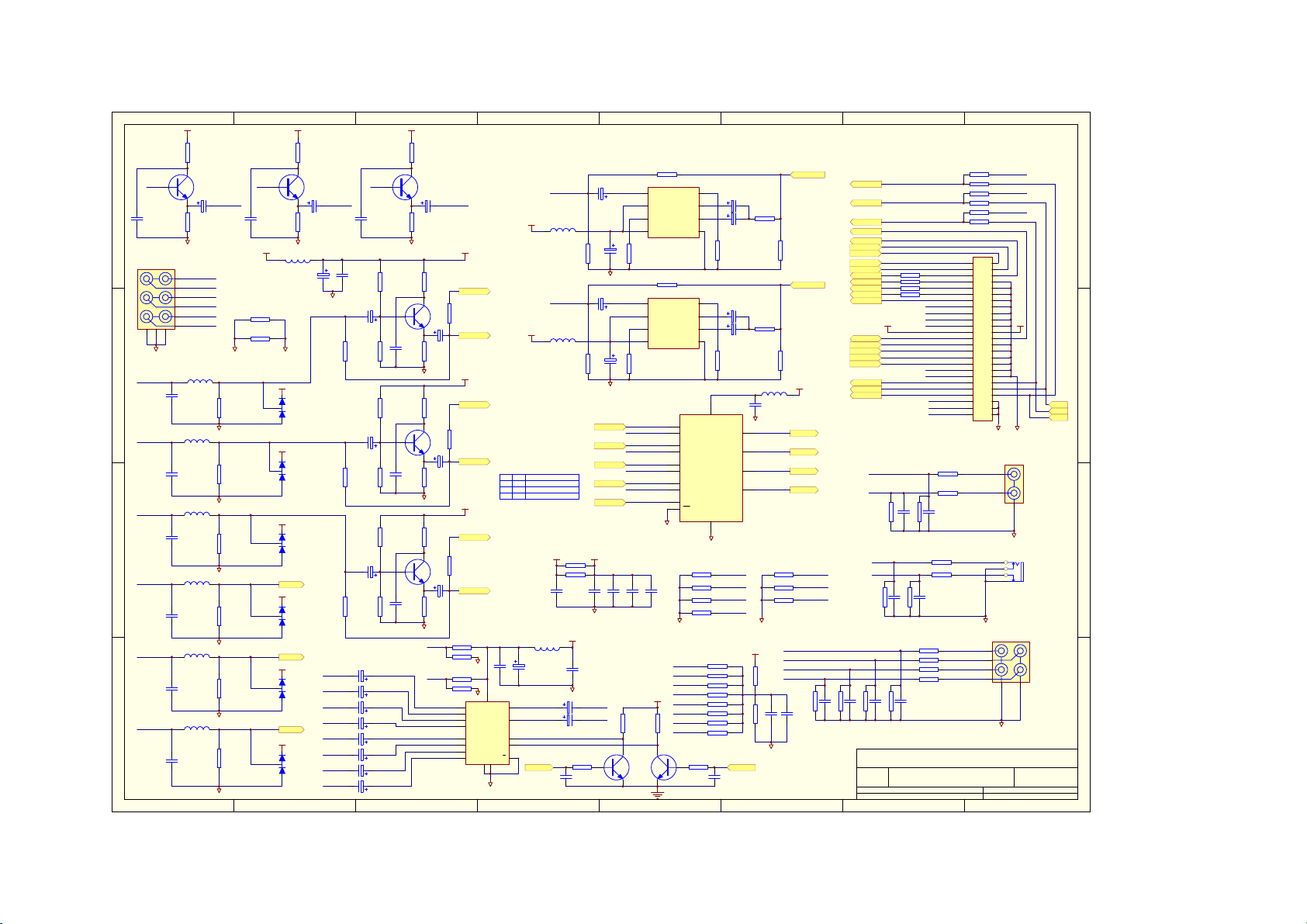
5V_E
28/101
R748
Cb
Q733
D
C760
JP701
8
7
9
SGND
C
Cb_in
Cr_in
YUV_Y_in
B
Pb_in
Pr_in
HD_Y_in
A
GYCbCr_Cb
C759
R749
SGND
2
Pr_in
1
Cr_in
4
Pb_in
3
Cb_in
6
HD_Y_in
5
YUV_Y_in
SGND AGND
L750
C740
L751
C742
L752
C744
L753
C746
L754
C748
L755
C750
1 2 3 4 5 6 78
SGND
SGND
SGND
SGND
SGND
SGND
Cb_in#
R750
Cr_in#
R751
YUV_Y_in#
R752
R753
R754
R755
5V_E
R761
Cr
Q734
C763
A5V
R741
R742
L738
5V
5V
5V
YPbPr_Pb
5V
YPbPr_Pr
5V
YPbPr_Y
5V
SGND
D701
D702
D703
D704
D705
D706
GYCbCr_Cr
C762
R763
C710
C711
SGND
C736
R736
C738
R737
C751
R738
DVI_R_IN#
VGA_R4#
YPbPr_R_IN#
YUV_R_IN#
DVI_L_IN#
VGA_L4#
YPbPr_L_IN#
YUV_L_IN#
5V_E
R765
Y
Q735
R767
C766
SGND
R719
Cb
Q701
R720 R722
C753
SGND
R723
Cr
Q702
R724
C754
SGND
R727
Y
Q703
R728
C755
SGND
C722
C723
C724 AV_R1
C726
AV_R2
AV_R3
AV_R4
C719
AV_L1
AV_L2
AV_L3
C720
AV_L4
C721
C725
R721
R725
R726
R729
R788
GYCbCr_Y
C765
R730
R731
R732
R_O
L_O
C737
C739
C752
R756
R757
R758
R759
12
14
15
11
1
5
2
5V_E
GYCbCr_Cb
VYCbCr_Cb
5V_E
GYCbCr_Cr
VYCbCr_Cr
5V_E
GYCbCr_Y
VYCbCr_Y
AGND
AGND
Y0A
Y1A
Y2A
Y3A
Y0B
Y1B
Y2B
Y3B4E
P15V330 Truth Table
8V_4052
16
U701
ZA
VDD
ZB
A1
A0
VEE7VSS
8
AGND
U702
1
TV_M
L748
A5V
TV_S
L749
A5V
IN EN
ON Switch
00
S1A S1B S1C S1D
S2A S2B S2C S2D10
x1Disabled
A5V
L756
C790C789
13
C756
R_O
3
C757
L_O
9
10
6
SEL1 SEL0
SEL1 SEL0
C701
VIN
2
ENABLE
3
RFC
VCC4GND
R787
R790
R794
R791
+8V
C787
AGND
AV_ROUT
AV_LOUT
R792 R793
R701
C702
Cutoff requency : 6.4MHz
SGND
U703
1
C705
VIN
2
ENABLE
3
RFC
VCC4GND
R706
C706
Cutoff frequency : 6.4MHz
SGND
TT_R
TT_R
SC1_R
TT_G
TT_G
SC1_G
11
TT_B
TT_B
TT_FSO
TT_SEL
5V
C713C714
C715 C716 C718
SGND
Q704 Q705
SC1_B
TT_FSO
SC1_BOX
TT_SEL
8V_4052
SGND
R739R740
10
14
13
15
2
3
5
6
1
SGND
R705
GSEL
VOUT
R710
GSEL
VOUT
AV_R1
AV_R2
AV_R3
AV_R4
AV_L1
AV_L2
AV_L3
AV_L4
V_TVCVBS
8
C703
7
VF
6
C704
5
R702
G_TVCVBS
8
C707
7
VF
6
C708
5
R707
16
S1A
VCC
S2A
DA
S1B
U704
S2B
S1C
S2C
S1D
S2D
IN
EN
DB
DC
DD
GND
8
SGND
R772
SC2_BOX
R773
SC2_R
R774
SC2_G
R775
SC2_B
8V_4052
R72
R73
R74
R75
R76
R77
R78
R79
C741C743
SGND
R703
R708
4
7
9
12
SGND
R70
R71
L739
C709
V_TT_R
V_TT_G
V_TT_B
V_TT_FSO
R784
R785
R786
C780
AGND
V_TVCVBS
R704
G_TVCVBS
R709
A5V
V_TT_R
V_TT_G
V_TT_B
V_TT_FSO
YUV_L_IN#
YUV_R_IN#
YPbPr_L_IN#
YPbPr_R_IN#
C781
V2
C2
Y2
R715
C734
R716
G_SVideo_Y
G_SVideo_C
G_AVCVBS
SCL_S5V
SC2_SW
GPIO_P31
GPIO_P30
GPIO_P32
GPIO_P33
G_TT_FSO
G_TT_R
G_TT_G
G_TT_B
SC1_SW
SDA_S5V
3450_rest
SP_RELAY
3230_VO
V_AVCVBS
V_SVideo_C
V_SVideo_Y
C730
7654321
R735
R745
G_SVideo_Y
R734
R744
G_SVideo_C
R733
R743
G_AVCVBS
SCL_S5V
SC2_SW
GPIO_P31
GPIO_P30
GPIO_P32
49 50
GPIO_P33
47 48
45 46
SC2_BOX
R768
R769
R770
R771
MUTE
DVI_L_IN#
DVI_R_IN#
R711
C732
VGA_L4#
VGA_R4#
R714
R713
C729
R779
R783
R778
R782
R718
R717
C735
C731
Title
7-VIDEO&AUDIO IN
Number RevisionSize
A3
Date: 14-Oct-2005 Sheet of
File: F:\4228\4228_temp_ddb\4228_Temp.DDBDrawn By:
R712
C733
SC2_R
SC2_G
SC2_B
SC1_SW
SC1_BOX
SC1_R
SC1_G
SC1_B
SDA_S5V
3450_rest
MUTE
SP_RELAY
3230_VO
TV_M
TV_S
V_AVCVBS
V_SVideo_C
V_SVideo_Y
AV_LOUT
AV_ROUT
+8V
R776
R780
C728
R777
R781
43 44
41 42
39 40
37 38
35 36
33 34
31 32
29 30
27 28
25 26
23 24
21 22
19 20
17 18
15 16
13 14
11 12
9 10
7 8
5 6
3 4
1 2
JP703
DVI_L_IN
DVI_R_IN
VGA_L4
VGA_R4
YUV_L_IN
YUV_R_IN
YPbPr_L_IN
YPbPr_R_IN
JP705
AGND
3
1
4
2
V_SVideo_Y
V_SVideo_C
V_AVCVBS
AGND SGND
3
2
AGND
JP707
3
4
2
1
JP704
5
AGND
8
D
A5VA5V
V2
C2
Y2
1
6
C
C2
V2
Y2
B
A
Page 31

Audio.Board.BH(M-CH).05.06.14.sch-1 - Tue Aug 16 22:15:14 2005
29/101
Page 32

DUBHE OSD Ver1.1_NAKS.sch-1 - Mon Oct 18 11:47:11 2004
30/101
Page 33

0025.sch-1 - Mon May 16 09:25:50 2005
31/101
Page 34

Basic Operations & Circuit Description
32/101
MODULE
There are 1 pc. panel and 12 pc.s PCB including 2 pc.s Y/Z Sustainer board, 2 pc.s Y Drive
board, 6 pc.s X Extension boards, 1 pc. Control (Signal Input) and 1 pc. Power
board in the Module.
SET
There are 6 pc.s PCBs including 1 pc. AUX. PSU Board, 1 pc. Keypad board, 1 pc.
Remote Control Receiver board, 1 pc. L/R Speakers and 1 pc. Main (Video) board in the SET.
Page 35

33/101
Audio
Page 36

PCB function
34/101
1. Power:
(1). Input voltage: AC 100V~120V, 45Hz~60Hz.
Input range: AC 90V(Min)~265V(Max) auto regulation.
(2). To provide power for PCBs.
2. Main (Video InterFace) board: To converter TV signals, S signals, AV signals, Y Pb/
Cb Pr/Cr signals, DVI signals and D-SUB signals to digital ones and to transmit to
Control board.
3. Control board: Dealing with the digital signal for output to panel.
4. Y-Sustainer / Z-Sustainer board:
(1). Receiving the signals from Control and high voltage supply.
(2). Output scanning waveform for Module.
5. Y-Drive board: Receive signal from Y sustainer, output horizontal scanning waveform to the panel.
6. X extension board (6pcs): Output addressing signals.
7. Tuner/Audio Board
: :
: Process and Amplifying the audio signal to speakers and
: :
convert TV RF signal to video/audio signal and send to Main board.
Page 37

PCB failure analysis
35/101
1. CONTROL : a. Abnormal noise on screen. b. No picture.
2. MAIN (video) : a. Lacking color, Bad color scale.
b. No voice.
c. No picture but with signals output, OSD and back light.
d. Abnormal noise on screen.
3. POWER : No picture, no power output.
4. Z - Sustainer : a. No picture.
b. Color not enough.
c. Flash on screen.
5. Y - Sustainer : Darker picture with signals.
6. X - Extension : Abormal vertical noise on screen.
7. Audio Board or AUX PSU: a. No voice. (Make sure Mute/OFF) .
b. Noise.
Page 38

Basic operation of Plasma Display
36/101
1. After turning on power switch, power board sends 5Vst-by Volt to Micro Processor
2. The micro Processor memorize the last state of Power, When the last state of
power is on or receive power on signal from local Key or Remote control, Micro
Processor will send on control signal to power. Then Power sends (5Vsc, 9Vsc,
24V and RLYON, Vs ON) to PCBs working. This time VIF will send signals to
display Image, OSD on the panel and start to search available signal sources.
If the audio signals input, them will be amplified by Audio AMP and transmitted to
Speakers.
3. If some abnormal signals are detected (for example: over volts, over current, over
temperature and under volts), the system will be shut down by Power off.
Page 39

Main IC Specifications
37/101
- PW181 Image Processor, Scaler
- PW1231 Digital Video Signal Processor
- VPC 323XD Comb-filter Video Processor
- Z86229 NTSC Line 21 CCD decorder
- MSP34x0G Multistandard Sound Processor
-AD9880 Analog/HDMI Dual Display Interface
-PI5V330 Wideband/Video Quad 2-Channel MUX/DEMUX
-SM5304AV Video Buffer with Built-in Analog LPF
-TDA2616 2 X 12 W hi-fi audio power amplifier with mute
-SAA5360 Multi page intelligent teletext decoder
-AT24C32 Z-Wire Serial EEPROM
-HT48R06A-1 8-Bit Cost-Effective I/O Type MCU
Page 40

PW181
38/101
Product Specification
General Description
The PW181 ImageProcessor is a highly integrated
“system-on-a-chip” that interfaces computer graphics and
video inputs in virtually any format to a fixed-frequency flat
panel display.
Computer and video images from NTSC/PAL to WUXGA
at virtually any refresh rate can be resized to fit on a fixedfrequency target display device with any resolution up to
WUXGA. Video data from 4:3 aspect ratio NTSC or PAL
and 16:9 aspect ratio HDTV or SDTV is supported. Multiregion, nonlinear scaling allows these inputs to be resized
optimally for the native resolution of the display.
Advanced scaling techniques are supported, such as
format conversion using multiple programmable regions.
Three independent image scalers coupled with frame
locking circuitry and dual programmable color lookup
tables create sharp images in multiple windows, without
user intervention.
Embedded SDRAM frame buffers and memory controllers
perform frame rate conversion and enhanced video
processing completely on-chip. A separate memory is
dedicated to storage of on-screen display images and
CPU general purpose use.
Advanced video processing techniques are supported
using the internal frame buffer, including motion adaptive,
temporal deinterlacing with film mode detection. When
used in combination with the new third-generation scaler,
this advanced video processing technology delivers the
highest quality video for advanced displays.
Both input ports support integrated DVI 1.0 content
protection using standard DVI receivers.
A new advanced OSD Generator with more colors and
larger sizes supports more demanding OSD applications,
such as on-screen programming guides. When coupled
with the new, faster, integrated microprocessor, this OSD
Generator supports advanced OSD animation techniques.
Video
TV
Signal
Input
TV Tu n e r
Com puter
Video
Decoder
ADC/
TMDS
Crystal
PW181
TV
Signal
Com puter
TV Tu n e r
Video
Input
ADC/
TMDS
Video
Decoder
PW181 System Block Diagram
ROM
Features
• Third-generation, two-dimensional filtering techniques
• Third-generation, advanced scaling techniques
• Second-generation Automatic Image Optimization
• Frame rate conversion
• Video processing
• On-Screen Display (OSD)
• On-chip microprocessor
• JTAG debugger and boundary scan
• Picture-in-picture (PIP)
• Multi-region, non-linear scaling
• Hardware 2-wire serial bus support
Applications
• Multimedia Displays
• Plasma Displays
• Digital Television
Device Application Package
PW181-10V Up to XGA Displays
PW181-20V Up to UXGA Displays
352 PBGA
Dis pla y
Programmable features include the user interface, custom
start-up screen, all automatic imaging features, and
special screen effects.
PRELIMINARY / CONFIDENTIAL
Page 41

110 MSPS/140 MSPS Analog Interface
39/101
a
FEATURES
140 MSPS Maximum Conversion Rate
300 MHz Analog Bandwidth
0.5 V to 1.0 V Analog Input Range
500 ps p-p PLL Clock Jitter at 110 MSPS
3.3 V Power Supply
Full Sync Processing
Sync Detect for “Hot Plugging”
Midscale Clamping
Power-Down Mode
Low Power: 500 mW Typical
4:2:2 Output Format Mode
APPLICATIONS
RGB Graphics Processing
LCD Monitors and Projectors
Plasma Display Panels
Scan Converters
Microdisplays
Digital TV
R
AIN
G
AIN
B
AIN
HSYNC
COAST
CLAMP
FILT
SCL
SDA
for Flat Panel Displays
FUNCTIONAL BLOCK DIAGRAM
CLAMP
CLAMP
CLAMP
SYNC
PROCESSING
AND CLOCK
GENERATION
SERIAL REGISTER
AND
A
0
POWER MANAGEMENT
A/D
A/D
A/D
AD9883A
AD9883A
8
8
8
REF
R
OUTA
G
OUTA
B
OUTA
MIDSCV
DTACK
HSOUT
VSOUT
SOGOUT
REF
BYPASS
GENERAL DESCRIPTION
The AD9883A is a complete 8-bit, 140 MSPS monolithic analog
interface optimized for capturing RGB graphics signals from
personal computers and workstations. Its 140 MSPS encode
rate capability and full power analog bandwidth of 300 MHz
supports resolutions up to SXGA (1280 × 1024 at 75 Hz).
The AD9883A includes a 140 MHz triple ADC with internal
1.25 V reference, a PLL, and programmable gain, offset, and
clamp control. The user provides only a 3.3 V power supply,
analog input, and Hsync and COAST signals. Three-state
CMOS outputs may be powered from 2.5 V to 3.3 V.
The AD9883A’s on-chip PLL generates a pixel clock from the
Hsync input. Pixel clock output frequencies range from 12 MHz to
140 MHz. PLL clock jitter is 500 ps p-p typical at 140 MSPS.
When the COAST signal is presented, the PLL maintains its
output frequency in the absence of Hsync. A sampling phase
adjustment is provided. Data, Hsync, and clock output phase
relationships are maintained. The AD9883A also offers full sync
processing for composite sync and sync-on-green applications.
A clamp signal is generated internally or may be provided by
the user through the CLAMP input pin. This interface is fully
programmable via a 2-wire serial interface.
Fabricated in an advanced CMOS process, the AD9883A is
provided in a space-saving 80-lead LQFP surface-mount plastic
package and is specified over the 0°C to 70°C temperature range.
REV. A
Information furnished by Analog Devices is believed to be accurate and
reliable. However, no responsibility is assumed by Analog Devices for its
use, nor for any infringements of patents or other rights of third parties that
may result from its use. No license is granted by implication or otherwise
under any patent or patent rights of Analog Devices.
One Technology Way, P.O. Box 9106, Norwood, MA 02062-9106, U.S.A.
Tel:
Fax:
Page 42

PW1231A
40/101
Product Specification
General
The PW1231A is a high-quality, digital video signal
processor that incorporates Pixelworks’ patented
deinterlacing, scaling, and video enhancement
algorithms. The PW1231A accepts industry-standard
video formats and resolutions, and converts the input into
many desired output formats.The highly efficient video
algorithms result in excellent quality video.
The PW1231A combines many functions into a single
device, including a memory controller, auto-configuration,
and others. This high level of integration enables simple,
flexible, cost-effective solutions that require fewer
components.
Crysta l
Video
PW1231A
System Block Dia gra m
Video
Decoder
PW1231A
PW1231AL
SDRAM
Digital
Output
Features
• Built-In Memory Controller
• Motion-Adaptive Deinterlace Processor
• Intelligent Edge Deinterlacing
• Digital Color/Luminance Transient Improvement (DCTI/DLTI)
• Interlaced Video Input Options, including NTSC and PAL
• Independent horizontal and vertical scaling
• Copy Protection
• Two-Wire Serial Interface
8100 SW Nyberg Road
Tualatin, OR 97062 USA
Telephone: 503.612.6700
FAX: 503.612.6713
www.pixelworks.com
Applications:
For use with Digital Displays
• Flat-Panel (LCD, DLP) TVs
• Rear Projection TVs
• Plasma Displays
• LCD Multimedia Monitors
• Multimedia Projectors
Device Application Package
PW1231A
PW1231AL
NOTE: “L” denotes lead (Pb) free
Up to XGA 160-pin PQF
P/N 001-0097-00 Rev B
PRELIMINARY—CONFIDENTIAL
July 2003
Page 43

41/101
a
Analog/HDMI Dual Display Interface
Preliminary Datasheet 3/26/2004 AD9880
FEATURES
Analog/HDMI Dual Interface
Supports High-Bandwidth Digital Content Protection
RGB to YCbCr two-way color conversion
Automated clamping level adjustment
1.8/3.3V Power Supply
100-pin LQFP Pb-Free Package
RGB and YCbCr Output Formats
Analog Interface
8-bit Triple Analog to Digital Converters
150 MSPS Maximum Conversion Rate
Macrovision Detection
2:1 Input Mux
Full Sync Processing
Sync Detect for “Hot Plugging”
Mid-Scale Clamping
Digital Video Interface
HDMI 1.0, DVI 1.0
150 MHz HDMI Receiver
Supports High-Bandwidth Digital Content Protection
(HDCP 1.1)
Digital Audio Interface
HDMI 1.0 compatible audio interface
S/PDIF (IEC90658 compatible) digital audio output
Multi-channel I
APPLICATIONS
Advanced TV
HDTV
Projectors
LCD Monitor
GENERAL DESCRIPTION
The AD9880 offers designers the flexibility of an analog interface
and High-Definition Multimedia Interface (HDMI) receiver
integrated on a single chip. Also included is support for High
bandwidth Digital Content Protection (HDCP).
Analog Interface
The AD9880 is a complete 8-bit 150 MSPS monolithic analog
interface optimized for capturing Component Video (YPbPr) and
RGB graphics signals. Its 150 MSPS encode rate capability and
full power analog bandwidth of 300 MHz supports all HDTV
formats (up to 1080p) and FPD resolutions up to SXGA (1280 x
1024 at 75 Hz).
The analog interface includes a 150 MHz triple ADC with
internal 1.25V reference, a Phase Locked Loop (PLL), and
programmable gain, offset, and clamp control. The user provides
only 1.8V and 3.3V power supply, analog input, and Hsync.
Three-state CMOS outputs may be powered from 1.8V to 3.3V.
The AD9880’s on-chip PLL generates a pixel clock from Hsync.
Pixel clock output frequencies range from 12 MHz to 150 MHz.
S audio output (up to 8 channels)
2
FUNCTIONAL BLOCK DIAGRAM
HSYNC 0
HSYNC 1
HSYNC 0
HSYNC 1
SOGIN 0
SOGIN 1
COAST
CLAMP
CKINV
CKEXT
FILT
RX0+
RX1+
RX2+
RXC+
RXCR
DDCSCL
DDCSDA
SDA
RX0-
RX1-
RX2-
MCL
MDA
IN0
IN1
SCL
TERM
Analog Interface
2:1
Clamp
MUX
2:1
MUX
2:1
MUX
2:1
Processing and
MUX
Serial Register and
Power Management
Digital Interface
HDMI Receiver
HDCP
Sync
Clock
Generation
R/G/B or YPbPr
R/G/B or YPbPr
PLL clock jitter is typically less than 500 ps p-p at 150 MHz. The
AD9880 also offers full sync processing for composite sync and
Sync-on-Green (SOG) applications.
Digital Interface
The AD9880 contains a HDMI 1.0 compatible receiver and
supports all HDTV formats (up to 1080p) and display resolutions
up to SXGA (1280 x 1024 at 75 Hz). The receiver features an
intra-pair skew tolerance of up to one full clock cycle. With the
inclusion of HDCP, displays may now receive encrypted video
content. The AD9880 allows for authentication of a video receiver,
decryption of encoded data at the receiver, and renewability of that
authentication during transmission as specified by the HDCP 1.1
protocol.
Fabricated in an advanced CMOS process, the AD9880 is provided
in a space-saving 100-lead LQFP surface-mount plastic package
and is specified over the 0 ºC to 70 ºC temperature range.
A/D
REFOUT
REFIN
R/G/B 8X3
or YCbCr
2
R/G/B 8X3
or YCbCr
2
DATACK
HSOUT
VSOUT
SOGOUT
Ref
DATACK
DE
Hsync
Vsync
MUXES
AD9880
R/G/B 8X3
YCbCr (4:2:2
or 4:4:4)
2
RGB ÅÆYCbCr Ma trix
SPDIF OUT
8 Channel
I
MCLK
LRCLK
2S OUT
DATACK
HSOUT
VSOUT
SOGOUT
DE
/A0
AD9880 Preliminary Technical Information
Information furnished by Analog Devices is believed to be accurate and reliable.
However, no responsibility is assumed by Analog Devices for its use, nor for any
infringements of patents or other rights of third parties which may result from its
use. No license is granted by implication or otherwise under any patent or patent
rights of Analog Devices.
Analog Devices, Inc., 2004
One Technology Way, P.O Box 9106, Norwood, MA 02062–9106, USA
Tel: 617/329–4700 Fax: 617–326–8703
Page 44

PRELIMINARY DATA SHEET VPC 323xD
42/101
Comb Filter Video Processor
1. Introduction
The VPC 323xD is a high-quality, single-chip video
front-end, which is targeted for 4: 3 and 16:9, 50/60-Hz
and 100/120 Hz TV sets. It can be combined with other
members of the DIGIT3000 IC family (such as
DDP 331x) and/or it can be used with 3rd-party products.
The main features of the VPC 323xD are
– high-performance adaptive 4H comb filter Y/C sepa-
rator with adjustable vertical peaking
– multi-standard color decoder PAL/NTSC/SECAM
including all substandards
– four CVBS, one S-VHS input, one CVBS output
– two RGB/YC
component inputs, one Fast Blank
rCb
(FB) input
– integrated high-quality A/D converters and associ-
ated clamp and AGC circuits
– multi-standard sync process ing
– linear horizontal scaling (0.25 ... 4), as well as
non-linear horizontal scaling ‘Panoramavision’
– PAL+ preprocessing
– peaking, contrast, brightness , color saturation and
tint for RGB/YC
and CVBS/S-VHS
rCb
– high-qual ity soft mixer controlled by Fast Blank
1
1
1
---
-- -
– PIP processing for four picture sizes ( , or
1
---
of normal size) with 8-bit resolution
36
,,
4
----- -
9
16
– 15 predefined PIP display configurations and expert
mode (fully programmable)
– control interface for external field memory
2
C-bus interface
–I
– one 20.25-MHz crystal, few external components
– 80-pin PQFP pack age
1.1. System Architecture
Fig.1–1 shows the block diagram of the video processor
– li ne-locked c lock, data and sync, or 656-output
interface
CIN
VIN1
VIN2
VIN3
VIN4
VOUT
RGB/
YCrCb
FB
RGB/
YCrCb
Analog
Front-end
AGC
2×ADC
Analog
Component
Front-End
4 x ADC
Adaptive
Comb
Filter
NTSC
PAL
Y/G
Processing
U/B
V/R
FB FB
Matrix
Contrast
Saturation
Brightness
Tint
Y
Cr
Cb
Color
Decoder
NTSC
PAL
SECAM
Saturation
Tint
Y
Cr
Cb
Mixer
Y
2D Scaler
Panorama
Cr
Cb
Brightness
Clock
Gen.
PIP
Mode
Contrast
Peaking
2
C Bus
I
Output
Formatter
ITU-R 656
ITU-R 601
Memory
Control
Sync
+
Clock
Generation
Y OUT
CrCb
OUT
YCOE
FIFO
CNTL
LL C lock
H Sync
V Sync
AVO
Fig.1–1:Block diagram of the VPC323xD
Micronas
2
I
C Bus20.25 MHz
Page 45

43/101
4'.+/+0#4; 41&7%6#2'%+(+%#6+10
<
+0'
'%1&'4
• Complete Stand-Alone Line 21 Decoder for Closed-
Captioned and Extended Data Services (XDS)
• Preprogrammed to Provide Full Compliance with
EIA–608 Specifications for Extended Data Services
• Automatic Extraction and Serial Output of Special
XDS Packets (Time of Day, Local Time Zone, and
Program Blocking)
• Programmable XDS Filter for a Specific XDS Packet
• Cost-Effective Solution for NTSC Violence Blocking
inside Picture-in-Picture (PiP) Windows
!"
#$%
&%
" '
• Minimal Communications and Control Overhead Pro-
vide Simple Implementation of Violence Blocking,
Closed Captioning, and Auto Clock Set Features
• Programmable, On-Screen Display (OSD) for Creat-
ing Full Screen OSD or Captions inside a Picture-inPicture (PiP) Window
• User-Programmable Horizontal Display Position for
easy OSD Centering and Adjustment
2
• I
C Serial Data and Control Communication
• Supports 2 Selectable I
2
C Addresses
Capable of processing Vertical Blanking Interval (VBI)
data from both fields of the video frame in data, the Z86229
Line 21 Decoder offers a feature-rich solution for any television or set-top application. The robust nature of the
Z86229 helpsthe device conformto the transmissionformat
defined in the Television Decoder Circuits Act of 1990, and
in accordance with the Electronics Industry Association
specification 608 (EIA–608).
The Line 21 data stream can consist of data from several data
channels multiplexed together. Field 1 consists of four data
channels: two Captions and two Texts. Field 2 consists of
five additional data channels: two Captions, two Texts, and
Extended Data Services (XDS). The XDS data structure is
defined in EIA–608. The Z86229 can recover and display
data transmitted on any of these nine data channels.
The Z86229 can recover and output to a host processor via
2
C serial bus. The recovered XDS data packet isfurther
the I
defined in the EIA–608 specification. The on-chip XDS filters in the Z86229 are fully programmable, enabling recovery ofonly those XDS datapackets selectedby the user.This
functionality allows the device to extract the required XDS
information with proper XDS filter setup for compatibility
in a variety of TVs, VCRs, and Set-Top boxes.
In addition, the Z86229 is ideally suited to monitor Line 21
video displayed in a PiP window for violence blocking,
CCD, and other XDS data services. A block diagram of the
Z86229 is illustrated in Figure 1.
Page 46

PRELIMINARY DATA SHEET MSP 34x0G
Multistandard Sound Processor Family
Release Note: Revision bars indicate significant
changes to the previous edition. The hardware and
software description in this document is valid for
the MSP 34x0G version B8 and following versions.
1. Introduction
The MSP 34x0G family of single-chip Multistandard
Sound Processors covers the sound processing of all
analog TV-Standards worldwide, as well as the NICAM
digital sound standar ds. The full TV sound process ing ,
starting with analog sound IF signal-in, down to processed analog AF-out, is performed on a single chip.
Figure 1–1 shows a simplified functional block diagram
of the MSP 34x0G.
This new generation of TV sound processing ICs now
includes versions for processing the multichan nel television sound (MTS) signal conforming to the standard
recommended by the Broadcast Television Systems
Committee (BTSC). The DBX noise reduction, or alternatively, Micronas Noise Reduction (MNR) is performed alignment free.
Other processed standards are the Japanese FM-FM
multiplex standard (EIA-J) and the FM Stereo Radio
standard.
Current ICs have to perform adjustment procedu res in
order to achieve good stereo sepa ration for BTSC and
EIA-J. The MSP 34x0G has optimum stereo performance without any adjustments.
All MSP 34xxG versions are pin compatible to the
MSP 34xxD. Only minor modifications are necessary
to adapt a MSP 34xxD controlling software to the
MSP 34xxG. The MSP 34x0G further simplifies controlling software. St andard selection requi res a single
2
C transmission only.
I
The MSP 34x0G has built-in automatic functions: The
IC is able to detect the actual sound standard automatically (Automatic Standard Detection). Furthermore,
pilot levels and identification sign als can be evaluated
internally with subsequent switching between mono/
stereo/bilingual; no I
2
C interaction is necessar y (Auto-
matic Sound Selectio n) .
The MSP 3 4x0G can handle very high FM deviations
even in conjunction with NICAM processing. This is
especially impor tant for the introduction of NICAM in
China.
The ICs are produced in submicron CMOS technology.
The MSP 34x0G is available in the following packages:
PLCC68 (not intended for new design), PSDIP64,
PSDIP52, PQFP80, and PLQFP64.
Sound IF1
Sound IF2
I2S1
I2S2
SCART1
SCART2
SCART3
SCART4
MONO
ADC
SCART
DSP
Input
Select
De-
modulator
ADC
Pre-
processing
Prescale
Prescale
Fig. 1–1: Simplified functional block diagram of the MSP 34x0G
Loud-
speaker
Sound
Processing
Headphone
Sound
Processing
Source Select
DAC
DAC
DAC
DAC
SCART
Output
Select
Loudspeaker
Subwoofer
Headphone
I2S
SCART1
SCART2
Micronas
Page 47

12345678901234567890123456789012123456789012345678901234567890121234567890123456789012345678901212345678901234567890123456789012123456789012
12345678901234567890123456789012123456789012345678901234567890121234567890123456789012345678901212345678901234567890123456789012123456789012
Product Features:
45/101
• High-performance, low-cost solution to switch
between video sources
• Wide bandwidth: 200 MHz
• Low ON-resistance: 3Ω
• Low crosstalk at 10 MHz: –58 dB
• Ultra-low quiescent power (0.1 µA typical)
• Single supply operation: +5.0V
• Fast switching: 10 ns
• High-current output: 100 mA
• Packages available:
– 16-pin 300-mil wide plastic SOIC (S)
– 16-pin 150-mil wide plastic SOIC (W)
– 16-pin 150-mil wide plastic QSOP (Q)
Functional Block Diagram
S1
S2
S1
S2
S1
S2
S1
S2
A
A
B
B
C
C
D
D
D
D
D
D
A
B
C
D
PI5V330
Low ON Resistance Wideband/Video
Quad 2-Channel MUX/DEMUX
Product Description:
Pericom Semiconductor’s PI5V series of mixed signal video
circuits are produced in the Company’s advanced CMOS
low-power technology, achieving industry leading performance.
The PI5V330 is a true bidirectional Quad 2-channel
multiplexer/demultiplexer that is recommended for both
RGB and composite video switching applications. The
VideoSwitch™ can be driven from a current output
RAMDAC or voltage output composite video source.
Low ON-resistance and wide bandwidth make it ideal for
video and other applications. Also this device has exceptionally high current capability which is far greater than most
analog switches offered today. A single 5V supply is all that
is required for operation.
The PI5V330 offers a high-performance, low-cost solution
to switch between video sources. The application section
describes the PI5V330 replacing the HC4053 multiplier and
buffer/amplifier.
16-Pin Product Configuration
S1
S2A
DA
S1B
S2B
DB
GND
1
IN
2
A
3
16-PIN
4
Q16
5
6
W16
7
8
S16
16
15
14
13
12
11
10
VCC
EN
D
S1
S2D
DD
S1C
S2C
9
DC
DECODER/DRIVERS
Product Pin Description
EN IN
Truth Table
EN IN ON Switch
00S1A, S1B, S1C, S1D
01S2A, S2B, S2C, S2D
1 X Disabled
Pin Name Description
S1A, S2A Analog Video I/O
S1B, S2B
S1C, S2C
S1D, S2D
IN Select Input
EN Enable
DA, DB, Analog Video I/O
DC, DD
GND Ground
VCC Power
1
PS7032C 08/07/97
Page 48

46/101
Page 49

47/101
Page 50

48/101
Page 51

49/101
Page 52

50/101
Page 53

51/101
Page 54

Features
52/101
• Low-Voltage and Standard-Voltage Operation
– 5.0 (V
– 2.7 (V
– 2.5 (V
– 1.8 (V
• Low-Power Devices (I
• Internally Organized 4096 x 8, 8192 x 8
• 2-Wire Serial Interface
• Schmitt Trigger, Filtered Inputs for Noise Suppression
• Bidirectional Data Transfer Protocol
• 100 kHz (1.8V, 2.5V, 2.7V) and 400 kHz (5V) Clock Rate
• Write Protect Pin for Hardware Data Protection
• 32-Byte Page Write Mode (Partial Page Writes Allowed)
• Self-Timed Write Cycle (10 ms max)
• High Reliability
– Endurance: 1 Million Write Cycles
– Data Retention: 100 Years
– ESD Protection: >3,000V
• Automotive Grade and Extended Temperature Devices Available
• 8-Pin JEDEC PDIP, 8-Pin JEDEC SOIC, 8-Pin EIAJ SOIC,
and 8-pin TSSOP Packages
= 4.5V to 5.5V)
CC
= 2.7V to 5.5V)
CC
= 2.5V to 5.5V)
CC
= 1.8V to 5.5V)
CC
= 2=µA @ 5.5V) Available
SB
2-Wire
Serial EEPROM
32K (4096 x 8)
64K (8192 x 8)
AT24C32
Description
The AT24C32/64 provides 32,768/65,536 bits of serial electrically erasable and programmable read only memory (EEPROM) organized as 4096/8192 words of 8 bits
each. The device’s cascadable feature allows up to 8 devices to share a common 2wire bus. The device is optimized for use in many industrial and commercial applications where low power and low voltage operation are essential. The AT24C32/64 is
available in space saving 8-pin JEDEC PDIP, 8-pin JEDEC SOIC, 8-pin EIAJ SOIC,
and 8-pin TSSOP (AT24C64) packages and is accessed via a 2-wire serial interface.
In addition, the entire family is available in 5.0V (4.5V to 5.5V), 2.7V (2.7V to 5.5V),
2.5V (2.5V to 5.5V) and 1.8V (1.8V to 5.5V) versions.
Pin Configurations
A0
A1
A2
8-Pin TSSOP
1
2
3
4
8-Pin SOIC
8
VCC
7
WP
6
SCL
5
SDA
Pin Name Function
A0 - A2 Address Inputs
SDA Serial Data
SCL Serial Clock Input
WP Write Protect
8-Pin PDIP
GND
AT24C64
2-Wire, 32K
Serial E
2
PROM
A0
A1
A2
GND
1
1
2
3
4
8
VCC
7
WP
6
SCL
5
SDA
A0
A1
A2
GND
2
3
4
VCC
8
WP
7
SCL
6
SDA
5
Rev. 0336G–04/01
1
Page 55

Absolute Maximum Ratings*
53/101
Operating Temperature.................................. -55°C to +125°C
Storage Temperature ..................................... -65°C to +150°C
Voltage on Any Pin
with Respect to Ground.....................................-1.0V to +7.0V
Maximum Operating Voltage .......................................... 6.25V
DC Output Current........................................................ 5.0 mA
Block Diagram
*NOTICE: Stresses beyond those listed under “Absolute
Maximum Ratings” may cause permanent damage to the device. This is a stress rating only and
functional operation of the device at these or any
other conditions beyond those indicated in the
operational sections of this specification is not
implied. Exposure to absolute maximum rating
conditions for extended periods may affect
device reliability.
Pin Description
SERIAL CLOCK (SCL): The SCL input is used to positive
edge clock data into each EEPROM device and negative
edge clock data out of each device.
SERIAL DATA (SDA): The SDA pin is bidirectional for
serial data transfer. This pin is open-drain driven and may
be wire-ORed with any number of other open-drain or open
collector devices.
DEVICE/PAGE ADDRESSES (A2, A1, A0): The A2, A1
and A0 pins are device address inputs that are hard wired
or left not connected for hardware compatibility with
AT24C16. When the pins are hardwired, as many as eight
32K/64K devices may be addressed on a single bus system (device addressing is discussed in detail under the
2
AT24C32/64
Device Addressing section). When the pins are not hardwired, the default A
WRITE PROTECT (WP): The write protect input, when tied
to GND, allows normal write operations. When WP is tied
high to V
(8/16K bits) of memory are inhibited. If left unconnected,
WP is internally pulled down to GND.
, all write operations to the upper quandrant
CC
, A1, and A0 are zero.
2
Memory Organization
AT24C32/64, 32K/64K SERIAL EEPROM: The 32K/64K is
internally organized as 256 pages of 32 bytes each. Random word addressing requires a 12/13 bit data word
address.
Page 56

Features
54/101
·
Operating voltage:
f
=4MHz: 2.2V~5.5V
SYS
f
=8MHz: 3.3V~5.5V
SYS
·
13 bidirectional I/O lines
·
An interrupt input shared with an I/O line
·
8-bit programmable timer/event counter with overflow interrupt and 8-stage prescaler
·
On-chip crystal and RC oscillator
·
Watchdog Timer
·
1024´14 program memory ROM
·
64´8 data memory RAM
·
Buzzer driving pair and PFD supported
General Description
The HT48R06A-1/HT48C06 are 8-bit high performance, RISC architecture microcontroller devices specifically designed for cost-effective multiple I/O control
product applications. The mask version HT48C06 is
fully pin and functionally compatible with the OTP version HT48R06A-1 device.
HT48R06A-1/HT48C06
8-Bit Cost-Effective I/O Type MCU
·
HALT function and wake-up feature reduce power
consumption
·
Up to 0.5ms instruction cycle with 8MHz system clock
at V
=5V
DD
·
Allinstructions in one or two machine cycles
·
14-bit table read instruction
·
Two-level subroutine nesting
·
Bit manipulation instruction
·
63 powerful instructions
·
Low voltage reset function
·
16-pin SSOP package
18-pin DIP/SOP package
The advantages of low power consumption, I/O flexibility, timer functions, oscillator options, HALT and
wake-up functions, watchdog timer, buzzer driver, as
well aslow cost, enhance the versatility of these devices
to suit a wide range of application possibilities such as
industrial control, consumer products, subsystem controllers, etc.
Block Diagram
P r o g r a m
R O M
I n s t r u c t i o n
R e g i s t e r
I n s t r u c t i o n
D e c o d e r
T i m i n g
G e n e r a t o r
O S C 2 O S C 1
R E S
V D D
V S S
P r o g r a m
C o u n t e r
M P
A L U
S h i f t e r
A C C
S T A C K 0
S T A C K 1
M U X
I N T / P C 0
I n t e r r u p t
C i r c u i t
T M R
I N T C
P C 0
M
D A T A
U
M e m o r y
X
S T A T U S
T M R C
W D T S
W D T P r e s c a l e r
P O R T C
P C C
P C
P B C
P B
P A C
P A
B Z / B Z
P O R T B
P O R T A
M
U
X
W D T
P r e s c a l e r
T M R / P C 1
P C 1
P C 0 ~ P C 1
P B 0 ~ P B 2
P A 0 ~ P A 7
M
U
X
f
R C O S C
f
S Y S
/ 4
S Y S
Rev. 1.30 1 August 7, 2003
Page 57

Pin Assignment
55/101
HT48R06A-1/HT48C06
P B 0 / B Z
P C 0 / I N T
P C 1 / T M R
Pad Assignment
HT48C06
P A 3
P A 2
P A 1
P A 0
V S S
1
2
3
4
5
6
7
8
P A 4
1 6
P A 5
1 5
P A 6
1 4
P A 7
1 3
O S C 2
1 2
O S C 1
1 1
V D D
1 0
R E S
9
H T 4 8 R 0 6 A - 1 / H T 4 8 C 0 6
1 6 S S O P - A
1
P A 0
2
P B 2
P B 1 / B Z
3
P A 3
P A 2
P A 1
P A 0
P B 2
P B 1 / B Z
P B 0 / B Z
V S S
P C 0 / I N T
1
2
3
4
5
6
7
8
9
P A 4
1 8
P A 5
1 7
P A 6
1 6
P A 7
1 5
O S C 2
1 4
O S C 1
1 3
V D D
1 2
R E S
1 1
1 0
P C 1 / T M R
H T 4 8 R 0 6 A - 1 / H T 4 8 C 0 6
1 8 D I P - A / S O P - A
P A 6
P A 5
P A 4
P A 3
P A 2
P A 1
1 3
1 4
1 5
1 8
1 61 7
( 0 , 0 )
P A 7
1 2
1 1
O S C 2
9
4
P B 0 / B Z
6
7
5
V S S
P C 0 / I N T
8
R E S
P C 1 / T M R
1 0
V D D
O S C 1
* The IC substrate should be connected to VSS in the PCB layout artwork.
Rev. 1.30 2 August 7, 2003
Page 58

Pad Description
56/101
Pad Name I/O Options Description
PA0~PA7 I/O
PB0/BZ
PB1/BZ
PB2
VSS
PC0/INT
PC1/TMR
RES
VDD
OSC1
OSC2
* All pull-high resistors are controlled by an option bit.
Pull-high*
Wake-up
Pull-high*
I/O
I/O or BZ/BZ
¾¾
I/O Pull-high*
I
¾¾
I
O
¾
Crystal
or RC
Bidirectional 8-bit input/output port. Each bit can be configured as wake-up
input by options. Software instructions determine the CMOS output or
Schmitt trigger input with a pull-high resistor (determined by pull-high op
tions).
Bidirectional 3-bit input/output port. Software instructions determine the
CMOS output or Schmitt trigger input with a pull-high resistor (determined by
pull-high options).
The PB0 and PB1 are pin-shared with the BZ and BZ
PB0 and PB1 are selected as buzzer driving outputs, the output signals come
from an internal PFD generator (shared with a timer/event counter).
Negative power supply, ground
Bidirectional I/O lines. Software instructions determine the CMOS output or
Schmitt trigger input with a pull-high resistor (determined by pull-high options). The external interrupt and timer input are pin-shared with the PC0 and
PC1, respectively. The external interrupt input is activated on a high to low
transition.
Schmitt trigger reset input. Active low
Positive power supply
OSC1, OSC2 are connected to an RC network or Crystal (determined by options) for the internal system clock. In the case of RC operation, OSC2 is the
output terminal for 1/4 system clock.
HT48R06A-1/HT48C06
-
, respectively. Once the
Absolute Maximum Ratings
Supply Voltage...........................VSS-0.3V to VSS+6.0V
Input Voltage..............................V
Note: These are stress ratings only. Stresses exceeding the range specified under ²Absolute Maximum Ratings² may
cause substantial damage to the device. Functional operation of this device at other conditions beyond those
listed in the specification is not implied and prolonged exposure to extreme conditions may affect device reliability.
-0.3V to VDD+0.3V
SS
Storage Temperature ............................-50°Cto125°C
Operating Temperature...........................-40°Cto85°C
Rev. 1.30 3 August 7, 2003
Page 59

HT48R06A-1/HT48C06
57/101
D.C. Characteristics
Symbol Parameter
V
I
DD1
I
DD2
I
DD3
I
STB1
I
STB2
V
V
V
V
V
I
OL
I
OH
R
DD
IL1
IH1
IL2
IH2
LVR
PH
Operating Voltage
Operating Current (Crystal OSC)
Operating Current (RC OSC)
Operating Current (Crystal OSC) 5V
Standby Current (WDT Enabled)
Standby Current (WDT Disabled)
Input Low Voltage for I/O Ports,
TMR and INT
Input High Voltage for I/O Ports,
TMR and INT
Input Low Voltage (RES)
Input High Voltage (RES)
Low Voltage Reset
I/O Port Sink Current
I/O Port Source Current
Pull-high Resistance
Test Conditions
V
DD
¾
¾
3V
5V
3V
5V
Conditions
=4MHz
f
SYS
=8MHz
f
SYS
No load, f
No load, f
No load, f
SYS
SYS
SYS
=4MHz
=4MHz
=8MHz
3V
No load, system HALT
5V
3V
No load, system HALT
5V
¾¾
¾¾
¾¾
¾¾
enabled
LVR
¾
3V
V
=0.1V
OL
OH
=0.9V
DD
DD
¾
¾
5V 10 20
3V
V
5V
3V
5V
Min. Typ. Max. Unit
2.2
3.3
¾
¾
¾
¾
¾
¾¾
¾¾
¾¾
¾¾
0
0.7V
DD
0
0.9V
DD
2.7 3.0 3.3 V
48
-2 -4 ¾
-5 -10 ¾
40 60 80
10 30 50
Ta=25°C
5.5 V
¾
5.5 V
¾
0.6 1.5 mA
24mA
0.8 1.5 mA
2.5 4 mA
35mA
5
mA
10
0.3V
¾
V
¾
0.4V
¾
V
¾
¾
¾
1
2
DD
DD
DD
DD
mA
mA
mA
V
V
V
V
mA
mA
mA
mA
kW
kW
Rev. 1.30 4 August 7, 2003
Page 60

Samsung SDI Co. Ltd. A/S Manual Plasma Display Module
58/101
DATE: Jun 24, 2005
CUSTOMER’S A/S MANUAL
107cm (42 Inch) Wide Plasma Display Module
MODEL : 42″SD V4 PDP
(S42SD-YD07)
Quality Innovation Team
Page 61

Samsung SDI Co. Ltd. A/S Manual Plasma Display Module
59/101
PDP Division, Samsung SDI
1. Overview
1-1 Model Name of plasma Display
1-2 External View
1-3 Specifications
2. Precaution
2-1 Handling Precaution for Plasma Display,
2-2
Safety Precautions for Service (Handling, prevention of a electrical shock, measure against
power outage, etc)
CONTENTS
3. Name & Function
3-1 Layout of Assemblies
3-2 Block Diagram:
3-3 Main function of Each Assembly
3-4 Product/Serial Label Location
4. Operation checking after rectification
4-1 Flow chart
4-2 Defects , Symptoms and Detective Parts
5. Disassembling / Assembling
5-1 Tools and measurement equipment
5-2 Exploded View
5-3 Disassembling & Re-assembling
6. Operation Check after Repair Service
6-1 Check Item
6-2 Check Procedure
7. Operation Check
7-1 Adjustment Specification, Checking Position etc.
7-2 Adjusting procedure
Page 62

Samsung SDI Co. Ltd. A/S Manual Plasma Display Module
60/101
1. Overview
1-1 Model Name of Plasma Display
MODEL : 42″SD V4 PDP (S42SD-YD07)
1-2 External View
【 M3 = X Board + Y Board + Logic Board + SMPS 】
Page 63

Samsung SDI Co. Ltd. A/S Manual Plasma Display Module
61/101
1-3 Points of Screw Mount
Green Dot : SCREW 4X12
Red Dot : SCREW 3X10
Page 64

Samsung SDI Co. Ltd. A/S Manual Plasma Display Module
62/101
1-4 Specifications
No Item Specification
1 Pixel 852 (H) × 480 (V) pixels (1 pixel = 1 R,G,B cells)
2 Number of Cells 2556 (H) × 480 (V)
3 Pixel Pitch 1.095 (H) ㎜ × 1.110 (V) ㎜
R 0.365 (H) ㎜ × 1.110 (V) ㎜
4
Cell Pitch
G 0.365 (H) ㎜ × 1.110 (V) ㎜
B 0.365 (H) ㎜ × 1.110 (V) ㎜
5 Display size
932.940 (H) ㎜ × 532.800(V) ㎜
[ 36.73 inch × 20.98 inch ]
6 Screen size Diagonal 42" Color Plasma Display Module
7 Screen aspect 16 : 9
8 Display color 16.77 million colors
Over 160°
9 Viewing angle
(Angle with 50% and greater brightness perpendicular to PDP
module)
10 Dimensions 982 (W) × 582 (H) × 54 (D) ㎜
11 Weight Module 1 About 15.4 kg
12 Packing weight Module 1
233kg ± 5kg (including modules) /
11pcs/BOX
13 Packing size L 1175 * W 1140 * H 893 (mm) / 11pcs/BOX
60Hz/ 50Hz, LVDS
Broadcasting reception
14
Vertical frequency
and
Video/Logic Interface
Page 65

Samsung SDI Co. Ltd. A/S Manual Plasma Display Module
63/101
2. PRECAUTIONS
** To prevent the risks of unit damage, electrical shock and radiation, take the
following safety, service, and ESD precautions.
2-1 Handling Precautions for Plasma Display
PDP module use high voltage that is
dangerous to human. Before operating
PDP, always check the dust to prevent
circuit short. Be careful touching the
circuit device when power is on.
PDP module is sensitive to dust and
humidity. Therefore, assembling and
disassembling must be done in no dust
place.
PDP module has a lot of electric
devices. Service engineer must wear
PDP module use a fine pitch connector
which is only working by exactly
connecting with flat cable. Operator
must pay attention to a complete
connection when connector is
reconnected after repairing.
The capacitor’s remaining voltage in
the PDP module’s circuit board
temporarily remains after power is off.
Operator must wait for discharging of
remaining voltage during at least 1
equipment(for example , earth ring) to
prevent electric shock and working
clothes to prevent electrostatic.
minute.
2-2 Safety Precautions for Service (Handling, prevention of a electrical shock, measure
against power outage, etc)
( Safety Precautions )
Before replacing a board, discharge forcibly
The remaining electricity from board.
When connecting FFC and TCPs to the
module, recheck that they are perfectly
connected.
To prevent electrical shock, be careful not
to touch leads during circuit operations.
To prevent the Logic circuit from being
damaged due to wrong working, do not
connect/disconnect signal cables during
circuit operations.
Page 66

Samsung SDI Co. Ltd. A/S Manual Plasma Display Module
64/101
Do thoroughly adjustment of a voltage label
and voltage-insulation.
Before reinstalling the chassis and the
chassis assembly, be sure to use all
protective stuffs including a nonmetal
controlling handle and the covering of
partitioning type.
Caution for design change : Do not install
any additional devices to the module, and
do not change the electrical circuit design.
For example: Do not insert a subsidiary
audio or video connector. If you insert It, It
cause danger on safety. And, If you change
the design or insert, Manufactor guarantee
Examine carefully the cable status if it is
twisted or damaged or displaced. Do not
change the space between parts and circuit
board. Check the cord of AC power
preparing damage.
Product Safety Mark : Some of electric or
implement material have special
characteristics invisible that was related on
safety. In case of the parts are changed
with new one, even though the Voltage and
Watt is higher than before, the Safety and
Protection function will be lost.
The AC power always should be turned off,
before next repair..
will be not effect. .
If any parts of wire is overheats of damaged,
replace it with a new specified one
immediately, and identify the cause of the
problem and remove the possible
dangerous factors.
( Precaution when repairing ESD )
There is ESD which is easily damaged by
electrostatics.(for example Integrated circuit,
FET ) Electrostatic damage rate of product
will be reduced by the following technics
Check assembly condition of screw, parts
and wire arrangement after repairing.
Check whether the material around the
parts get damaged.
electric by ground connection, or must wear
the antistatic wrist-belt and ring. ( It must be
operated after removing dust on it – It
comes under precaution of electric shock.)
Before handling semiconductor
parts/assembly, must remove positive
Page 67

Samsung SDI Co. Ltd. A/S Manual Plasma Display Module
65/101
After removing ESD assembly, put on it with
aluminum stuff on the conductive surface to
prevent charging.
Do not use chemical stuff using Freon. It
generates positive electric that can damage
ESD.
Must use a soldering device for ground-tip
when soldering or de-soldering ESD.
Must use anti-static solder removal device.
Most removal device do not have antistatic
which can charge a enough positive electric
enough damaging ESD.
Before removeing the protective material
protective material into contact with the
chassis or assembly that the ESD is to be
installed on.
When handing an unpacked ESD for
replacement, do not move around too much.
Moving (legs on the carpet, for example)
generates enough electrostatic to damage
the ESD.
Do not take a new ESD from the protective
case until the ESD is ready to be installed.
Most ESD have a lead, which is easily
short-circuited by conductive materials
(such as conductive foam and aluminum)
from the lead of a new ESD, bring the
Page 68

7
66/101
Samsung SDI Co. Ltd. A/S Manual Plasma Display Module
3.NAME & FUNCTION
3-1 Layout of Assemblies
1
16
8
2
6
5
15
No. Location Name
1 SMPS SMPS
2 LOGIC-MAIN Board ASSY PCB LOGIC MAIN
3 X-MAIN Driving Board ASSY PCB X MAIN
3
174
10 9 11 121314
4 Y-MAIN Driving Board ASSY PCBY MAIN
5 LOGIC E BUFFER Board ASSY PCB BUFFER
6 LOGIC F BUFFER Board ASSY PCB BUFFER
7 Y-BUFFER (UPPER) Board ASSY PCB BUFFER
8 Y-BUFFER (DOWN) Board ASSY PCB BUFFER
9 LOGIC + Y-MAIN FFC CABLE-FLAT
10 LOGIC + X-MAIN FFC CABLE-FLAT
11 LOGIC + LOGIC BUF(E) FFC CABLE-FLAT
12 LOGIC + LOGIC BUF(F) FFC CABLE-FLAT
13 LOGIC BUF(E) + LOGIC BUF(F) LEAD CONNECTOR
14 SMPS + LOGIC BUF(E) LEAD CONNECTOR
15 SMPS + LOGIC MAIN LEAD CONNECTOR
16 SMPS + Y-MAIN LEAD CONNECTOR
17 SMPS + X-MAIN LEAD CONNECTOR
Page 69

Samsung SDI Co. Ltd. A/S Manual Plasma Display Module
67/101
1. SMPS 2. L-Main
3. X-Main 4. Y-Mian
5. Y-Buffer (Upper) 6. Y-Buffer (down)
7. E-Buffer
8. F-Buffer
Page 70

Samsung SDI Co. Ltd. A/S Manual Plasma Display Module
68/101
9. Logic + Y-Main 10. Logic + X-Main
11~12. LOGIC + LOGIC BUF 13. LOGIC BUF(E) + LOGIC BUF(F)
Page 71

Samsung SDI Co. Ltd. A/S Manual Plasma Display Module
69/101
3-2 BLOCK DIAGRAM
3-2-1 BLOCK DIAGRAM FOR DRIVE CIRCUIT OPERATION
To be Updated
3-2-2 Block Diagram for Logic circuit
Logic Main Block Diagram
Logic Main Block Diagram
LVDS
LVDS
INPU T
INPU T
(CLOCK
(CLOCK
R,G,B Data
R,G,B Data
V, H Sync.
V, H Sync.
DE)
DE)
I2C
I2C
Interfac e
Interfac e
Sig n al
Sig n al
ASIC
ASIC
SPS-S101
SPS-S101
128K
128K
DDR
DDR
128K
128K
DDR
DDR
X, Y
X, Y
FET
FET
Control
Control
TCP
TCP
CLK, DATA
CLK, DATA
Control
Control
Page 72

Samsung SDI Co. Ltd. A/S Manual Plasma Display Module
70/101
3-3 Main function of Each Assembly
■ X-main board : The X-main board generate a drive signal by switching the FET in synchronization with logic
main board timing and supplies the X electrode of the panel with the drive signal through the
connector.
1) Maintain voltage waveforms (including ERC)
2) Generate X rising ramp signal
3) Maintain Ve bias between Scan intervals
■.Y-main board : The Y-main board generate a drive signal by switching the FET in synchronization with the logic
Main Board timing and sequentially supplies the Y electrode of the panel with the drive signal
through the scan driver IC on the Y-buffer board. This board connected to the panel’s
Y terminal has the following main functions.
1) Maintain voltage waveforms (including ERC)
2) Generate Y-rising Falling Ramp
3) Maintain V scan bias
■ Logic main board : The logic main board generates and outputs the address drive output signal and the X ,Y
drive signal by processing the video signals. This Board buffers the address dirve output
signal and feeds it to the address drive IC (TCP module)
(video signal- X Y drive signal generation , frame memory circuit / address data rearrangement)
■.Logic buffer(E,F) : The logic buffer transmits data signal and control signal.
■.Y-buffer board (Upper, Lower) : The Y-buffer board consisting of the upper and lower boards supplies the
Y-terminal with scan waveforms. The board comprises 8 scan driver IC’s
(ST microelectronics STV 7617 : 64 or 65 output pins) , but 4 ICs for the SD class
■.AC Noise Filter : The AC Noise filter has function for removing noise(low Frequency) and blocking surge.
It effects Safety standards(EMC,EMI)
■.TCP( Tape Carrier Package ) : The TCP applies Va pulse to the address electrode and constitutes address
discharge by the potential difference between the Va pulse and the pulse
applied to the Y electrode. The TCP comprise 2 data driver Ics(STV7620A
:96 pins output pins) 14 TCPs are required for signal scan
.
Page 73

Samsung SDI Co. Ltd. A/S Manual Plasma Display Module
71/101
3-4 PRODUCT/ SERIAL LABEL LOCATION
Serial No.
Voltage label
3-4-1 Serial No.
* PANEL S/N
2 4 2 4 C 0 1 0 0 0 0 1
Serial No : 00001~99999
Date : 01~31
Month : 1~C
(Oct-A,Nov-B,Dec-C))
Year : 0 (2000) ~ 9 (2009)
Line No : 1 ~ 9 (0 : Pilot Line)
Type : 02~48 (ex.42SD V4 : 24)
(Step of even)
Page 74

Samsung SDI Co. Ltd. A/S Manual Plasma Display Module
72/101
4. OPERATION CHECKING AFTER RECTIFICATION
4-1 Flow chart
* A/S Check Point *
1.Checking the voltage for each assembly
2. Judging the Logic board working or not [LED 2000 blanking]
3. Adjusting the output signal through test points
4. Checking the panel’s crack
4-1-1 No voltage output
No vol tage output
Check Vol tage at CN8001/ 2pin
Connect [ 220Vac or 110Vac]
AC I nput
220 Vac or 11 0Vac
No
Reconnect i t
RL201 and RL202. act s?
Prot ect ion?
PSU
PSU
Yes
Yes
Yes
Check 5Vstb : 5.2V
No
Check D5V : 5. 2V
Check F101&F102
Replace PSU.
No
Check
out put vol t age
No
Page 75

Samsung SDI Co. Ltd. A/S Manual Plasma Display Module
73/101
st ep1. Open CN8 001
Check D5V : 5. 2V
Check Vs : 2 09V
Check Va : 70V
Check Vset : 198V
Check Vscan : - 180V
Check Ve : 100V
Check D3V3:3.4V
Check SB5V : 5. 2V
st ep2. Open CN8 002, CN8003
st ep3. Open CN8 006
st ep4. Open CN8 004
st ep5. Open CN8 007
st ep6. Reconnect CN8001
st ep7. Rest ar t PSU
PSU
No
Check Vs_on : 3. 0V
at CN8 008
Yes
GotoNo di spl ay.
Repl ace PSU.
Check F201&F301, F401, F501
Repl ace PSU.
Page 76

Samsung SDI Co. Ltd. A/S Manual Plasma Display Module
74/101
4-1-2 NO display (operating Voltage but an image doesn’t exist on Screen)
⇒ No Display is related with Y-MAIN, X-MAIN, Logic Main and so on.
This page shows you how to check the boards, and the following pages show you how to find
the defective board.
Logic Main
[LED 2000 Blinks]
Y – Main
Check
① LVDS Cable
② LED 2000;Green
③ Fuse F2000, F2001
No Display
Logic B’d
X – Main
Broken panel
Replace Logic B’d
Y-Ma in
Check
① F5001 for Vdd (5V)
17 / 3
② F5002 for Vcc (15V)
Fuse
Replace Logic B’d
OPEN
9
Page 77

Samsung SDI Co. Ltd. A/S Manual Plasma Display Module
y
75/101
Check
Q5011,13,14,15,16,17
Q5018,20,21,27
X-Main
SHORT
Replace Y-B’d
Replace Y-B’d
Check
① F4001 for Vdd (5V)
② F4002 for Vcc (15V)
Check
~
Fuse
FET
Panel
OPEN
SHORT
-
’
-
’
4-1-3 Abnormal Display (Abnormal Image is on Screen. (except abnormality in Sustain or Address)
⇒ Abnormal Display is related with Y-MAIN, X-MAIN, Logic Main and so on.
This page shows you how to check the boards, and the following pages show you how to find the
defective board.
18 / 39
Logic Main
[LED 2000 Blinks]
Abnormal
Displa
Y – Main X – Main
Page 78

Samsung SDI Co. Ltd. A/S Manual Plasma Display Module
76/101
Check
① F5001 for Vdd (5V)
② F5002 for Vcc (15V)
③ F5004 for Vs
Check
Q5011,13,14,15,16,17
Q5018,20,21,27
Q5028,29,32
Y-Ma in
Fuse
FET
X-Main
OPEN
Replace Y-B’d
SHORT
Replace
Check
① F4001 for Vdd (5V)
Fuse
② F4002 for Vcc (15V)
③ F4003 for Vs
Check
① Q4010 ~ Q4017
FET
OPEN
SHORT
-
’
-
’
Page 79

Samsung SDI Co. Ltd. A/S Manual Plasma Display Module
77/101
[Logic Main]
LED 2000 Blinks
Regular
Abnormal
Logic main
Replace
4-1-4 Sustain Open (some horizontal lines don’t exist on screen)
Page 80

Samsung SDI Co. Ltd. A/S Manual Plasma Display Module
78/101
After
Changing
Done
Page 81

Samsung SDI Co. Ltd. A/S Manual Plasma Display Module
79/101
4-1-5 Sustain Short ( some horizontal lines appear to be linked on Video )
[Y-FPC]
After
Changing
Done
4-1-6 Address Open ( some vertical lines don’t exist on screen )
⇒ Address Open is related with Logic Main, Logic Buffer, FFC, TCP and so on.
This page shows you how to check the boards, and the following pages show you how to find
the defective board.
Address Open
⇒ Line Open
⇒ Data Block Open
⇒
[ Logic Main/FFC ]
[ Logic Buffer ]
Changing necessary
Page 82

Samsung SDI Co. Ltd. A/S Manual Plasma Display Module
80/101
What is the status of open?
1 Line or
1 Block
NG
Half Block/
Half of
OK
Replace
PDP
NG
Replace
Logic Main/
Address Buffer
(E/F)
4-1-7 Address Short (some vertical lines appear to be linked on screen
⇒ Address Short is related with Logic Main, Logic Buffer, FFC, TCP and so on.
This page shows you how to check the boards, and the following pages show you how to find
OK
OK
the defective board.
[ Logic Main/FFC ]
Changing some parts
Address Open
⇒ Line Short
⇒
Data Block Short
[ Logic Buffer ]
Changing necessary
Parts (E/F)
Page 83

Samsung SDI Co. Ltd. A/S Manual Plasma Display Module
A
81/101
1 Line or
1 Block
Half Block/
Half of
Replace
Replace
Logic Main/
Address Buffer
4-2 DEFECTS, SYMPTONS AND DETECTIVE PARTS
Condition Name Description Related Board
■ No Voltage Output Operating Voltages don't exist. SMPS
■ No Display
■ Abnormal Display
■ Sustain Open
■ Sustain Short
Operating Voltages exist, but an Image
doesn't exist on screen
bnormal Image(not open or short) is on
screen.
some horizontal lines don't exist on
screen
some horizontal lines appear to be
linked on screen
Y-MAIN, X-MAIN, Logic Main, Cables
Y-MAIN, X-MAIN, Logic Main
Scan Buffer, FPC of X / Y
Scan Buffer, FPC of X / Y
■ Address Open some vertical lines don't exist on screen Logic Main, Logic Buffer, FFC,TCP
■ Address Short
some vertical lines appear to be linked
on screen
Logic Main, Logic Buffer ,FFC,TCP
Page 84

Samsung SDI Co. Ltd. A/S Manual Plasma Display Module
82/101
◈ Defect: Address(vertical stripe) Open ◈ Defect: Address(vertical stripe) Short
■ Symptom : A line or block does not light up in address
electrode direction.(1 line ,block open)
■Cause
① manufacturing : Panel electrode single line/
foreign material./electrostatic/
■ Symptom: Another color simultaneously appears because adjacent
data recognizes the single pattern signal
■Cause
① manufacturing : Panel electrode short / Foreign material
TCP defect
② Parts : TCP, Board connection defect
③ Operation : Assembly error / Film damage
conductive foreign object inside TCP
② Part : TCP/buffer defect lighting electrode cutting
defect
Page 85

Samsung SDI Co. Ltd. A/S Manual Plasma Display Module
83/101
◈ Defect: Address output error ◈ Defect: Sustain(horizontal stripe) Open
■ Symptom.: A defect other than address open
and short Data printout signal error
occurring at certain Gradation or pattern
■ Symptom : One or more line do not light up in Sustain direction
■Cause : ① manufacturing : .Panel bus electrode single line
FPC pressure defect
② Parts : FPC/board/connection disconnection
③ operation : assembly error.
Page 86

Samsung SDI Co. Ltd. A/S Manual Plasma Display Module
84/101
◈ Defect: Sustain(horizontal stripe) Short ◈ Defect: Dielectric material layer damage
■Symptom : Combined or adjacent lines are short in
sustain direction. The line appear brighter
than other at Ramp gradation pattern or low
gradation patter
■ Symptom: Burn caused by the damage of address bus dielectric
layer appears in the panel discharge/non discharge
area. sustain also open/short occurs by the damage
of address sustain printout
<Add Block and Line Open>
■Cause
① manufacturing : Panel electrode short/Foreign
material.
② Parts : Board/ connector/pin error
③ Operation : connector / assembling error
<Add and Sustain Open>
■Cause : layer uneven / abnormal voltage / foreign material
repair failed
Page 87

Samsung SDI Co. Ltd. A/S Manual Plasma Display Module
85/101
◈ Defect: F/White low discharge ◈ Defect: Weak discharge
■Symptom : Low discharge caused by unstable cells
occurring at full white pattern if high
(60 degree) or normal temperature.
■Symptom : Normal discharge but cells appear darker due to
weak light emission occurring mainly at low
(5 degree) Full white/Red/Green/Blue pattern
or gradation pattern
■ Cause
① Panel : MgO source / dielectric thickness
cell pitch/phosphor
② Circuit : drive waveform/ voltage condition
■ Cause
① Panel : MgO deposition count and thinckness /
aging condition
② Circuit : drive waveform/ voltage condition
Page 88

Samsung SDI Co. Ltd. A/S Manual Plasma Display Module
86/101
◈ Defect : panel damage ◈ Defect: Exhaust pipe damage
■ Symptom : Panel crack or break. No image appears in some
cause depending on the damaged parts and
damage level.
■ Symptom. : Crack in break if exhaust pipe
an image is partially lacking or the panel
noise occurs depending on the damaged parts
and with the passage of time
■ Cause
① Manufacturing : Flatness/palette pin interruption
② Operation : overload of panel corner / careless handling
③ Panel : Flatness / assembly error
■ Cause : Careless panel handling
Page 89

Samsung SDI Co. Ltd. A/S Manual Plasma Display Module
87/101
5. Disassembling / Assembling
5-1 Tools and measurement equipment
5-1-1. Tools
1) (+) type Screw Drivers : to screw the screws
2) Air Blower
3) Earth Ring
4) Small Driver : to adjust potentiometer
5) Dummy Discharge Resistor : 2.4kOhm/10W
5-1-2. Measuring Equipment
1) Oscilloscope : 500MHz sampling
2) Probe : 10:1
3) Digital Multi-meter
4) Signal Generator
5-3 Disassembling & Re-assembling
5-3-1 Disassembling & Re-assembling of FPC (Flexible Printed Circuit)
and Y-Buffer(Upper and Lower)
1. Removal procedures
1) Full out the FPC from Connector by holding the lead of the FPC with hands.
Page 90

Samsung SDI Co. Ltd. A/S Manual Plasma Display Module
88/101
2. Assembling Procedures
1) Push the lead of FPC with same strength until to be connected completely.
* Notice : Be careful do not get a damage on the connector pin during connecting by mistake.
5-3-2 Assembling & Disassembling of Flat Cable Connector of X-Main Board
1. Disassembling Procedure
1) Pull out the clamp of
connector.
2. Assembling Procedure
1) Put the Flat cable into the connector press
down lightly until locking sound (“Dack”)
comes out.
2) Pull Flat cable out
press down lightly.
3) Turn the Flat
cable reversely.
Page 91

Samsung SDI Co. Ltd. A/S Manual Plasma Display Module
89/101
5-3-3 Assembling & Disassembling the FFC and TCP from Connector
1. Disassembling of TCP
1) Open the clamp carefully.
2. Assembling of TCP
1) Put the TCP into the Connector carefully
* Notice : TCP and Connector was connected surely.
2) Pull the TCP out from Connector.
2) Close the clamp completely.
( The sound (“ Dack”) comes out. )
* Notice :
1) Checking whether the foreign material is on the Connector inside before assembling of TCP.
2) Be careful do not get a damage on the board by ESD during handling of TCP.
Page 92

Samsung SDI Co. Ltd. A/S Manual Plasma Display Module
90/101
3. Misassembling of TCP
1) The misassembling of TCP is the cause of defect.
4. Checking method of misassembling of TCP
1) Disconnecting address harness from CN8006 of LBE.
5. Assembling & Disassembling of FFC
( This is the photo of the assembling of FFC )
The procedure of assembling and disassembling of FFC is the same as TCP.
Page 93

Samsung SDI Co. Ltd. A/S Manual Plasma Display Module
91/101
5-3-4 Exchange of LBE, LBF board
2
1
3 4 5
( Photo 1 )
( Photo 2 )
1) Remove the screws in order of 2-4-1-5-3 from heat sink and then get rid of heat sink. ( Photo 1 )
2) Remove the TPC, FFC and power cable from the connectors.
3) Remove all of the screws from defected board.
4) Remove the defected board.
5) Replace the new board and then screw tightly.
6) Get rid of the foreign material from the connector.
7) Connect the TCP,FFC and power cable to the connector.
8) Reassemble the TCP heat sink.
9) Screw in order of 3-1-5-2-4. ( Photo 2 )
If you screw too tightly, it is possible to get damage on the Driver IC of TCP.
5-3-5 Exchange YBU, YBL and YM board
1) Separate all of the FPC connector of YBU (Y-Buffer upper) and YBL (Lower). ( Photo 1 )
2) Separate all of the connector of CN5003 and CN5004 from Y-Main. CN5407 from YBU and YBL
3) Loosen all of the screws of YBU, YBL and YM.
4) Remove the board from chassis.
Page 94

Samsung SDI Co. Ltd. A/S Manual Plasma Display Module
92/101
5) Remove the connector of CN5005, CN5006, CN5007 and CN5008 among YBU, YBL and YM.
6) Remove the YBL and YBU from Y-main.
7) Replace the defected board.
8) Reassemble the YBU and YBL to the Y-Main.
9) Connect the connector of CN5005, CN5006, CN5007 and CN5008 among YBU, YBL and YM.
10) Arrange the board on the chassis and then screw to fix.
11) Connect the FPC and YM of panel to the connector.
12) Supply the electric power to the module and then check the waveform of board.
13) Turn off the power after the waveform is adjusted.
Page 95

Samsung SDI Co. Ltd. A/S Manual Plasma Display Module
93/101
6. Operation Check after Repair Service
6-1 Check Item
Check Item Specification Remarks
TCP Assembling
condition
Module
assemble
check
6-2 Check Procedure
Drive board
Y BUFFER
Logic & Logic
Buffer
Harness Securely connected
Material Mixing No material mixing
Securely connected or
tightened
.
1) Visual check as following
a. Assembling condition of module.
b. No problem on the connection of module.
c. The grounding and easily short-circuited parts are not damaged.
2) Turn on the power to PDP module, and then check that LED lights up and the SET is working well.
3) Check the power voltage after turn on the power, and then check the Display condition by tapping slightly the Y-FPC 2 or 3 times.
4) Check whether something wrong during Full White Pattern period.
5) If something wrong, each voltage should be set to the standard voltage by using Multi-Tester and adjusting tools.
6) Adjust the waveform, using Oscilloscope for the waveform adjusting point.
7) Check the discharge of front panel by changing the image for each pattern.
8) Check the Low-discharge, Over-discharge and panel condition by adjusting the Pattern Generator Level.
9) Discharge still remain send back to SDI
Page 96

Samsung SDI Co. Ltd. A/S Manual Plasma Display Module
94/101
7. Operation Check
7-1 Adjustment Specification, Checking Position etc.
V4 TCP Ramp Waveform Inclination Adjustment ( Y-Board )
2
nd
Sub Fiend
Adjust VR5001 to set the time of
Yrr( Main Reset Rising Ramp ) 60㎲
Adjust VR5003 to set the time of
Yfr (Main Reset Falling Ramp) 80㎲
< Rising Ramp > <Falling Ramp>
Page 97

Samsung SDI Co. Ltd. A/S Manual Plasma Display Module
95/101
VR5003 Adjustment :
Falling Ramp flat time => Typ. 80usec
VR5001 Adjustment :
Rising Ramp flat time: Typ. 60usec
7-2 Adjusting procedure
1) 1) Get Pattern to be Full White.
2) Check the waveform using Oscilloscope
① Triggering through V_TOGG of LOGIC Board.
② Connect the OUT240 Test Point at the center of Y_buffer to other channel, and then check the 2nd SF operating waveform of
1TV-Field.
③ Check the waveform as before by adjusting Horizontal Division.
Check the Reset waveform when the V_TOGG Level is changed.
④ Set the Vset to 60us by adjusting VR5001.
⑤ Set the Falling maintenance time to 80us by adjusting R5003.
Page 98

Samsung SDI Co. Ltd. A/S Manual Plasma Display Module
96/101
Appendix 1. Adjust Voltage Level
No Output voltage(V) Voltage Setting (Normal Load) Output Voltage Variable Point
1 VS
2 VA
3 VE
4 VSET
5 VSCAN
6 VSB
7 VG
8 D5VL
9 D3V3
207V ± 1%
70V ± 1.5%
110V ± 1.5%
198V ± 1.5%
-185V ± 1.5%
5V ± 5%
15V ± 5%
5.2V ± 5%
3.3V ± 5%
195V ~ 215V
50V ~ 70V
70V ~ 110V
180V ~ 210V
-170V ~ -190V
Fixed
Fixed
Fixed
Fixed
Page 99

Spare Part List for PDP4206EM1 Date: 2006/01/05
97/101
Item Part Number Part Description
Usage /
unit
Unit
1 E6205-42SA02 DISPLAY PDP 42" 1 piece
2 900-420101-01B DISPLAY FILTER 42" 1 piece
3 771E42AA02-04 MAIN PCBA 1 set
4 771L42AA02-04 AUDIO PCBA 1 set
5 771-42AB01-01 KEY PCBA 1 set
6 771-42D110-01 IR RECEIVE PCBA 1 piece
7 E7801-080001 POWER PCBA 1 set
8 771-50AA05-01 SPEAK JACK PCBA 1 set
SPK ASSY FOR PD42HAA(LG) 16 OHM 7W
9 786-SPA103-01
1 set
R/L=1150MM/800MM EMI
10 E4101-027001 POWER SWITCH 1 piece
11 E4801-116002 SPEAKER 2 piece
12 E3219-002003 POWER SOCKET 1 piece
13 E3301-017002 TERMINAL PUSH WP2-19 2 piece
14 E3404-157001 AC POWER CORD 1 piece
15 E3421-927006
1 piece
POWER) FOR SDI
L=300MM 3WIRES FOR 42EAA POWER
AMP/AMP -2Y/550 (FROM SWITCH
16 E3421-927021
1 piece
CONNECT W/EMI
WIRE ASSY 5P 2.54MM
17 E3421-926042
1 piece
L=1150MM/800MM EMI
POWER CABLE 2Y/L=300MM FOR (SDI
18 E3421-926034
1 piece
50") (W/EMI)
WIRE ASSY 13P/6P+8P 2.0MM L=500MM
19 E3421-926041
1 piece
KEY/REMOTE (EMI)
WIRE ASSY L=245 31P(LVDS W-EMI) FOR
20 E3421-926077
1 piece
42" SDIV4
WIRE ASSY 2.5 8P/10P+4P L=280MM
21 E3421-926069
1 piece
EMI
22 E3421-926068 WIRE ASSY 2.5 9P/11P L=190MM EMI 1 piece
WIRE ASSY 4P/3P+3P 2.5MM
23 E3421-926071
1 piece
L=900MM/450MM EMI
24 E7501-052001 REMOTE 1 set
25 E7301-010002 AAA SIZE BATTERY 2 piece
26 200-42AA01-SMK01A FRONT CABINET BLACK 1 piece
208-SPA101-01R
27
SPEAKER BOX TOP CABINET 2 piece
28 209-SPA101-01R SPEAKER BOX BOTTOM CABINET 2 piece
29 277-42D101-01S FUNCTION KNOB 1 piece
30 263-42D101-01S POWER LENS 1 piece
Page 100

Spare Part List for PDP4206EM1 Date: 2006/01/05
98/101
Item Part Number Part Description
Usage /
unit
Unit
31 269-42D101-01L IR LENS 1 piece
32 481-50AA03-01S SHIELD BOX BOTTOM 1 piece
33 483-50AA01-01 SHIELD BOX COVER 1 piece
34 436-42AA07-01S TERMIAL SHEET 1 piece
35 402-42AA01-01S BACK COVER 1 piece
36 248-46D201-01 HANDLE FOR PLASMA 2 piece
37 734-BM0501-02 STAND BASE 1 set
38 510-42AA01-SMU01K CARTON BOX 1 piece
39 518-42AA01-01K BTM TRAY 1 piece
40 300-42AA03-01C POLYFOAM SHEET 2 piece
41 300-42AA01-02C POLYFOAM FOR BTM L&R 1 piece
42 300-42AA02-02C POLYFOM FOR TOP L&R 1 piece
43 244-34B811-01 GIFT BOX HANDLE 2 piece
44 310-504004-01 MAIN UNIT PLASTIC BAG 1 piece
INSTRUCTION MANUAL POLYBAG
45 310-151404-01T
1 piece
15"X14"X0.04MM
46 580-P42AAES-MU01L
1 piece
47 599-BM0502-01 IB SHEET E OF TEARDOWN 1 piece
48 388-42D103-01H CAUTION LABEL 1 piece
49 388-50AA01-01H SPEAKER L PLATE ENG (-/+) 1 piece
50 388-50AA01-02H SPEAKER R PLATE ENG (-/+) 1 piece
51 387-42AA01-SMU01H MODEL PLATE 1 piece
INT. SPEAKER LABEL FOR 786-SPA103-01
INSTRUCTION MANUAL
52 579-SPA101-15
1 piece
L
INT. SPEAKER LABEL FOR 786-SPA103-01
53 579-SPA101-16
1 piece
R
54 384-42AA01-SMU01H SHEET FOR TERMINAL 1 piece
55 590-42AA01-05 WARRANTY CARD 1 piece
56 593-42AA01-03 INSERTION CARD 1 piece
57 579-42D102-09 SERIAL NO/BAR CODE LABEL 1 piece
58 579-50AA02-01 DANGER CAUTION LABEL 1 piece
59 579-42AA01-07 BAR CODE LABEL 2 piece
579-42D105-01 PROTECTIVE EARTH LABEL 1 piece
60
61 568-P46T02-02 WARNING LB EN 1 piece
 Loading...