


CSD-A500
Table of contents
 Loading...
1
SERVICE MANUAL
CSD-A500
CD STEREO RADIO CASSETTE RECORDER
CD player section
System
Compact disc digital audio system
Laser diode properties
Material: GaAlAs
Wave length: 780 nm
Emission duration: Continuous
Laser output: Less than 44.6 µW
(This output is the value measured at a distance of
about 200 mm from the objective lens surface on
the optical pick-up block with 7 mm aperture.)
Spindle speed
200 r/min (rpm) to 500 r/min (rpm) (CLV)
Number of channels
2
Frequency response
20 - 20,000 Hz
Wow and flutter
Below measurable limit
Radio section
Frequency range
FM: 87.5 - 108 MHz
AM:531 - 1,611 kHz (9 kHz step)
530 - 1,610 kHz (10 kHz step)
IF
FM: 10.7 MHz
AM: 450 kHz
Antennas
FM: Telescopic aerial
AM: Built-in ferrite bar aerial
SPECIFICATIONS
Cassette recorder section
Recording system
4-track 2 channel stereo
Fast winding time
Approx. 120 sec. with Sony cassette C-60
Frequency response
TYPE I (normal): 80 - 10,000 Hz
General
Speaker
Full range: 8 cm dia.,
4 Ω, cone type (2)
Outputs
PHONES (Headphones) jack (stereo minijack):
For 16 - 68 Ω impedance headphones
Maximum power output
4 W
Power requirements
For the CD stereo radio cassette recorder:
230 V AC, 50 Hz (Singapore model)
120 V AC, 60 Hz (Taiwan model)
9 V DC, six R20 (size D) batteries
For the remote:
3 V DC, two R03 (size AAA) batteries
Ver 1.1 2004. 09
9-877-689-02
2004I04-1
© 2004. 09
E Model
CD
Model Name Using Similar Mechanism CSD-A300
Section
CD Mechanism Type KSM-213RDP
Optical Pick-up Name KSS-213R
TC
Model Name Using Similar Mechanism NEW
Section
Tape Transport Mechanism T ype MF-A500
– Continued on next page –
Sony Corporation
Personal Audio Company
Published by Sony Engineering Corporation

2
Power consumption
AC 15 W
Battery life
FM recording
Sony R20P: approx. 5.5 h
Sony alkaline LR20: approx. 13 h
Tape playback
Sony R20P: approx. 7.5 h
Sony alkaline LR20: approx. 15 h
CD playback
Sony R20P: approx. 2.5 h
Sony alkaline LR20: approx. 7 h
Dimensions
Approx. 358 × 152 × 246 mm (w/h/d)
(incl. projecting parts)
Mass
Approx. 3.7 kg (incl. batteries)
Supplied accessories
AC power cord (1)
Remote control (RM-Z1A001) (1)
Design and specifications are subject to change without
notice.
CSD-A500
SAFETY-RELATED COMPONENT WARNING!!
COMPONENTS IDENTIFIED BY MARK 0 OR DOTTED LINE
WITH MARK 0 ON THE SCHEMATIC DIAGRAMS AND IN
THE PARTS LIST ARE CRITICAL TO SAFE OPERATION.
REPLACE THESE COMPONENTS WITH SONY P ARTS WHOSE
PART NUMBERS APPEAR AS SHOWN IN THIS MANUAL OR
IN SUPPLEMENTS PUBLISHED BY SONY.
CAUTION
Use of controls or adjustments or performance of proce-
dures other than those specified herein may result in haz-
ardous radiation exposure.
Flexible Circuit Board Repairing
• Keep the temperature of the soldering iron around 270˚C during
repairing.
• Do not touch the soldering iron on the same conductor of the
circuit board (within 3 times).
• Be careful not to apply force on the conductor when soldering
or unsoldering.
Notes on Chip Component Replacement
• Never reuse a disconnected chip component.
• Notice that the minus side of a tantalum capacitor may be dam-
aged by heat.
NOTES ON HANDLING THE OPTICAL PICK-UP BLOCK
OR BASE UNIT
The laser diode in the optical pick-up block may suffer electrostatic
breakdown because of the potential difference generated by the
charged electrostatic load, etc. on clothing and the human body.
During repair, pay attention to electrostatic breakdown and also use
the procedure in the printed matter which is included in the repair
parts.
The flexible board is easily damaged and should be handled with
care.
NOTES ON LASER DIODE EMISSION CHECK
The laser beam on this model is concentrated so as to be focused on
the disc reflective surface by the objective lens in the optical pick-
up block. Therefore, when checking the laser diode emission,
observe from more than 30 cm away from the objective lens.

3
CSD-A500
6. DIAGRAMS
6-1. IC Pin Description............................................................. 27
6-2. Block Diagram – CD Section –......................................... 29
6-3. Block Diagram – Main Section –...................................... 30
6-4. Circuit Boards Location .................................................... 31
6-5. Printed Wiring Board – CD Section – ............................... 32
6-6. Schematic Diagram – CD Section –.................................. 33
6-7. Printed Wiring Board – Tuner Section – ........................... 34
6-8. Schematic Diagram – Tuner Section –.............................. 35
6-9. Schematic Diagram – Main Section (1/2) – ...................... 36
6-10. Schematic Diagram – Main Section (2/2) – ...................... 37
6-11. Printed Wiring Boards – Main Section – .......................... 38
6-12. Printed Wiring Board – TC Section – ............................... 39
6-13. Schematic Diagram – TC Section – .................................. 40
6-14. Printed Wiring Boards – Control Section –....................... 41
6-15. Schematic Diagram – Control Section – ........................... 42
6-16. Printed Wiring Boards – Power Supply Section – ............ 43
6-17. Schematic Diagram – Power Supply Section –................. 44
6-18. IC Block Diagrams............................................................ 45
7. EXPLODED VIEWS
7-1. Cabinet Section ................................................................. 48
7-2. Cabinet (Bottom) Section.................................................. 49
7-3. Cabinet Front Section........................................................ 50
7-4. Cabinet Top (1) Section ..................................................... 51
7-5. Cabinet Top (2) Section ..................................................... 52
7-6. Cabinet Top (3) Section ..................................................... 53
7-7. Cabinet Top (4) Section ..................................................... 54
7-8. Tape Mechanism Section .................................................. 55
7-9. CD Mechanism Section .................................................... 56
8. ELECTRICAL P ARTS LIST......................................... 57
1. SERVICING NOTES......................................................... 4
2. GENERAL
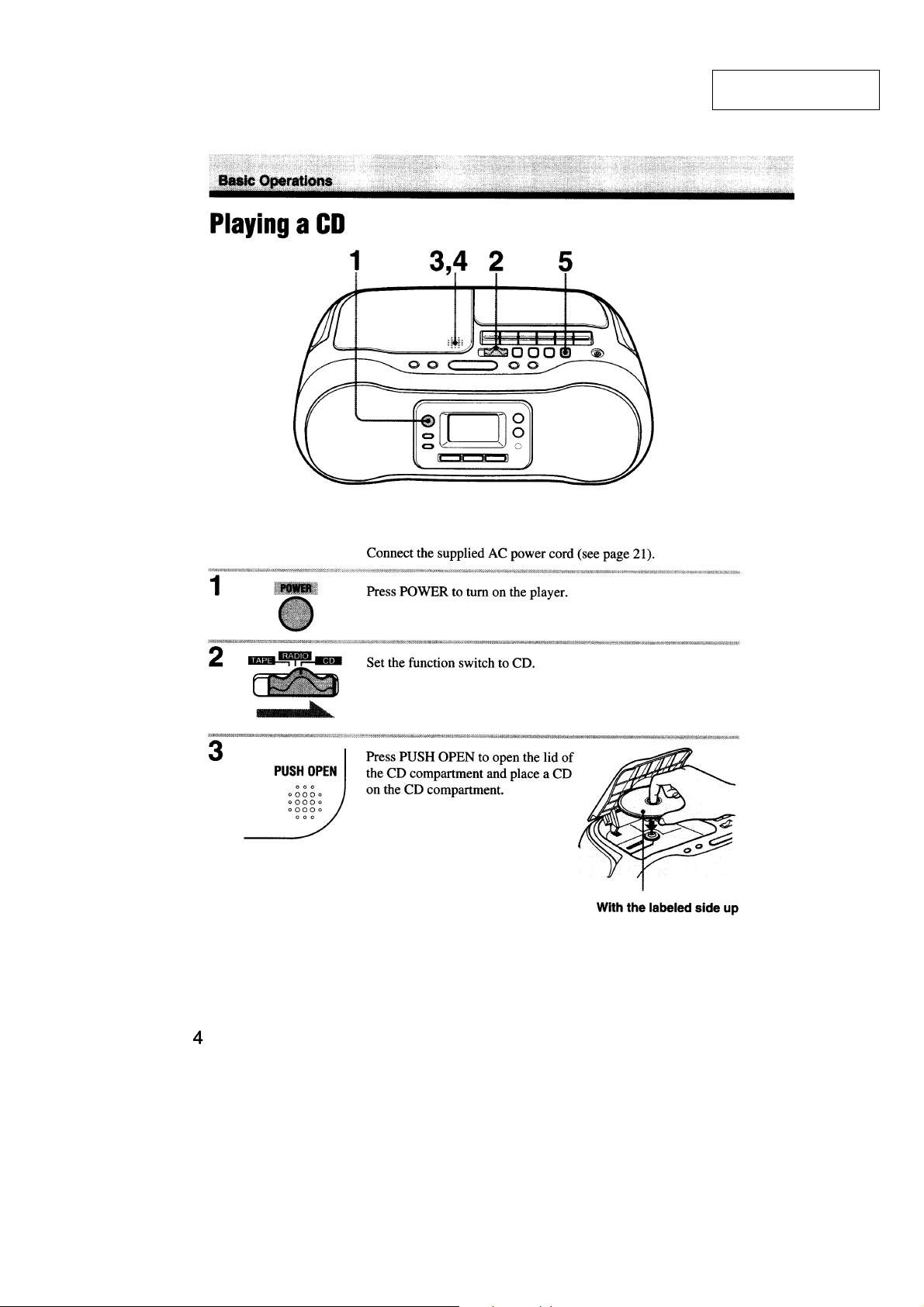
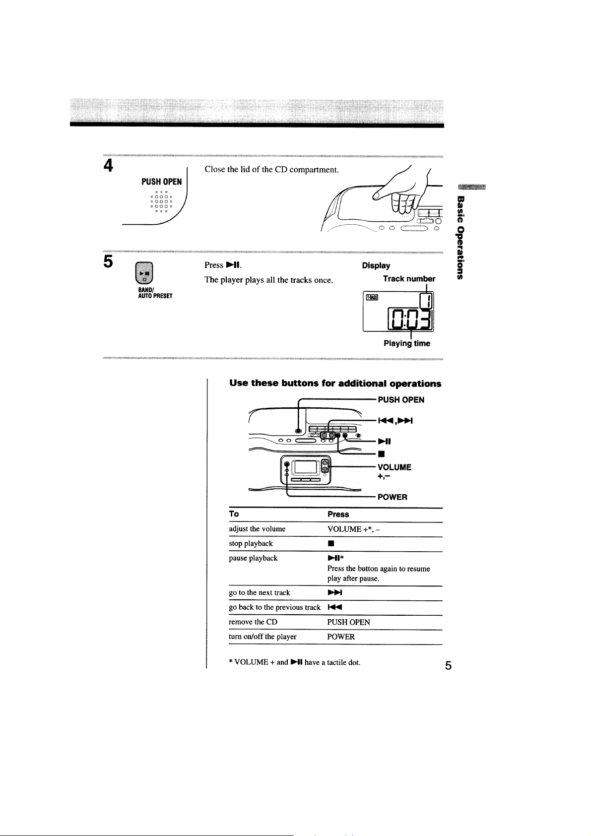
Playing a CD ........................................................................... 5
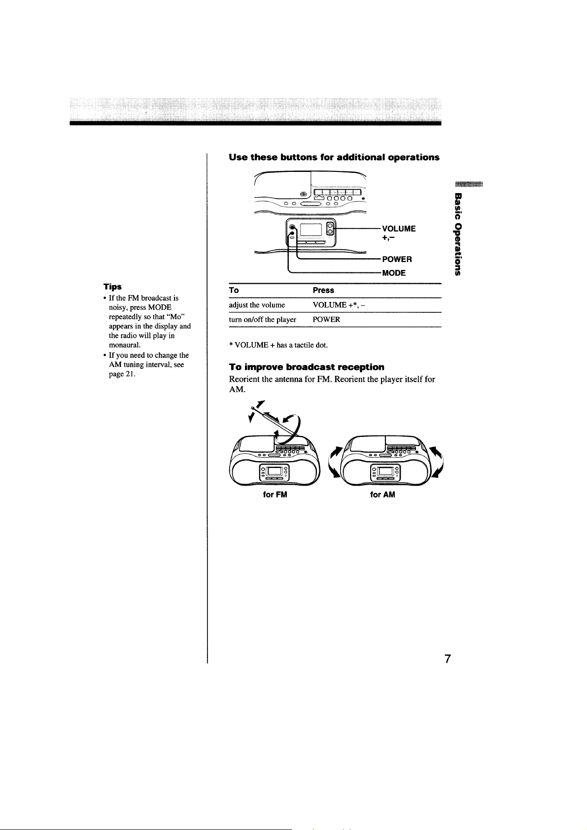
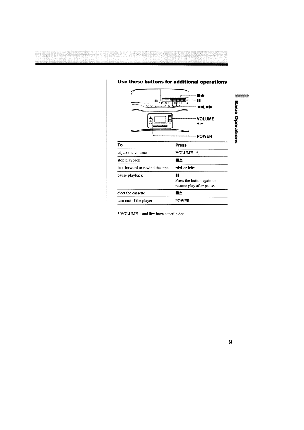
Listening to the radio............................................................... 7
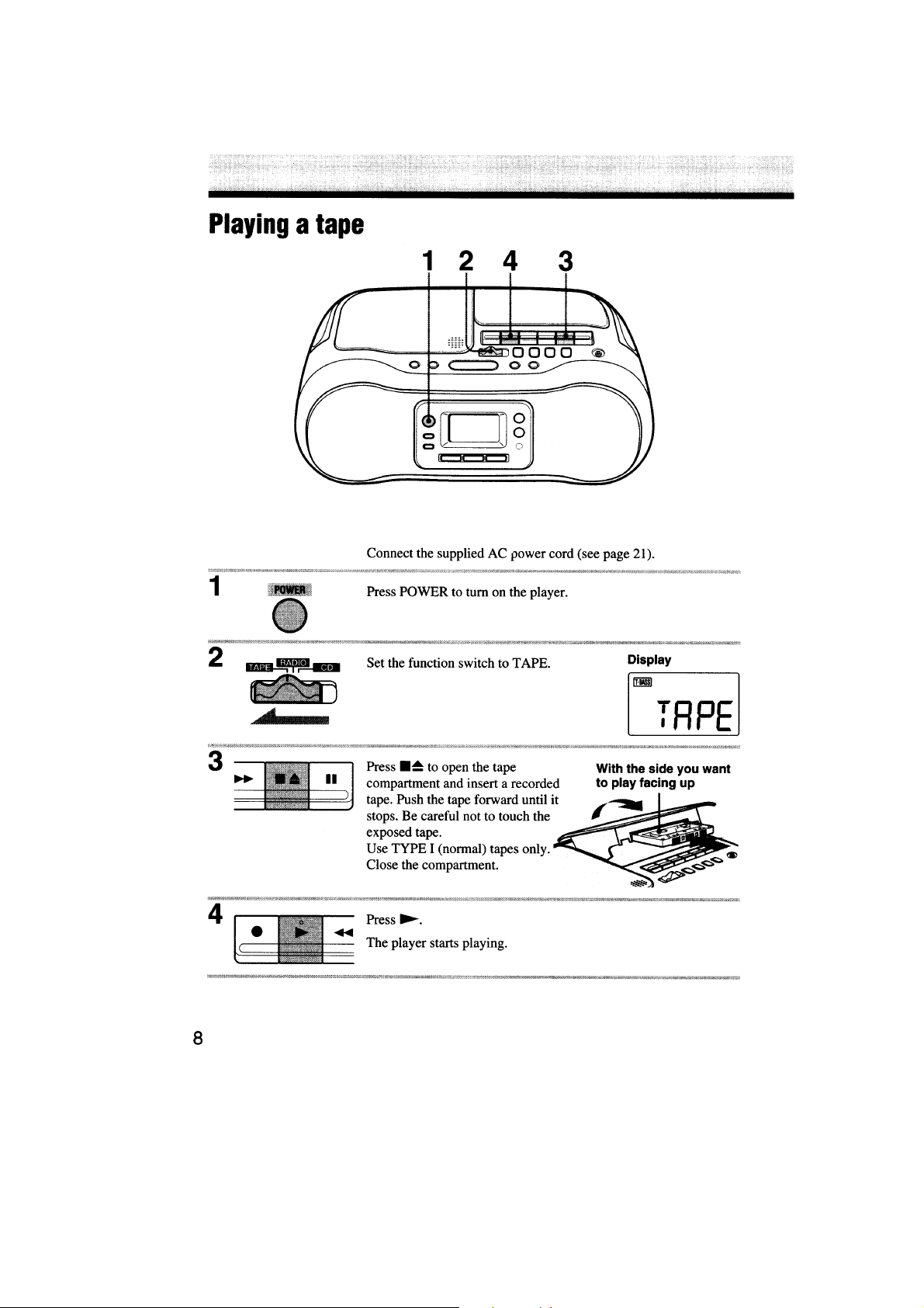
Playing a tape .......................................................................... 9
Recording on a tape ............................................................... 11
Setting the clock .................................................................... 13
3. DISASSEMBL Y
3-1. Cabinet (Bottom) Assy...................................................... 15
3-2. Cabinet (Top) Assy, Cabinet (Front) Assy ........................ 15
3-3. LCD Board, Light Board .................................................. 16
3-4. Button (Preset) .................................................................. 16
3-5. Transformer Board ............................................................ 17
3-6. Tuner Board....................................................................... 17
3-7. Main Board, H/P Board .................................................... 18
3-8. Key Board ......................................................................... 18
3-9. MD Block Assy................................................................. 19
3-10. Cassette Lid ....................................................................... 19
3-11. TC Board ........................................................................... 20
3-12. HRP301, HE301, Pinch Roller Arm Assy ......................... 20
3-13. M801, Belt ........................................................................ 21
3-14. CD Block Assy.................................................................. 21
3-15. CD Lid............................................................................... 22
3-16. CD Board .......................................................................... 22
3-17. Optical Pick-up ................................................................. 23
4. MECHANICAL ADJUSTMENTS............................... 24
5. ELECTRICAL ADJUSTMENTS
Tape Section .......................................................................... 24
Tuner Section......................................................................... 25
CD Section ............................................................................ 26
TABLE OF CONTENTS

4
CSD-A500
CHUCK PLATE JIG ON REPAIRING
On repairing CD section, playing a disc without the lid (CD), use
Chuck Plate Jig.
• Code number of Chuck Plate Jig: X-4918-255-1
SECTION 1
SERVICING NOTES
LASER DIODE AND FOCUS SEARCH OPERATION
CHECK
1. Turn ON the [POWER] button and press [CD] button to
CD position.
2. Open the CD lid.
3. Turn on S801 with screwdriver, etc. as following figure.
4. Press the N X (CD) button.
5. Confirm the laser diode emission while observing the objecting
lens. When there is no emission, Auto P ower Control circuit or
Optical Pick-up is broken.
Objective lens moves up and do wn three times for focus search.
S801
PRECAUTION TO REPLACE OPTICAL BLOCK
(KSM-213RDP)
Body or clothes electrostatic potential could ruin laser diode
in the optical block. Be sure ground body and workbench,
and use care the clothes do not touch the diode.
1) After the connection, remove solder shown in the right figure.
solder
5
CSD-A500
SECTION 2
GENERAL
This section is extracted
from instruction manual.
6
CSD-A500

7
CSD-A500
8
CSD-A500
9
CSD-A500
10
CSD-A500

11
CSD-A500
12
CSD-A500
13
CSD-A500

14
CSD-A500
• The equipment can be removed using the following procedure.
SECTION 3
DISASSEMBLY
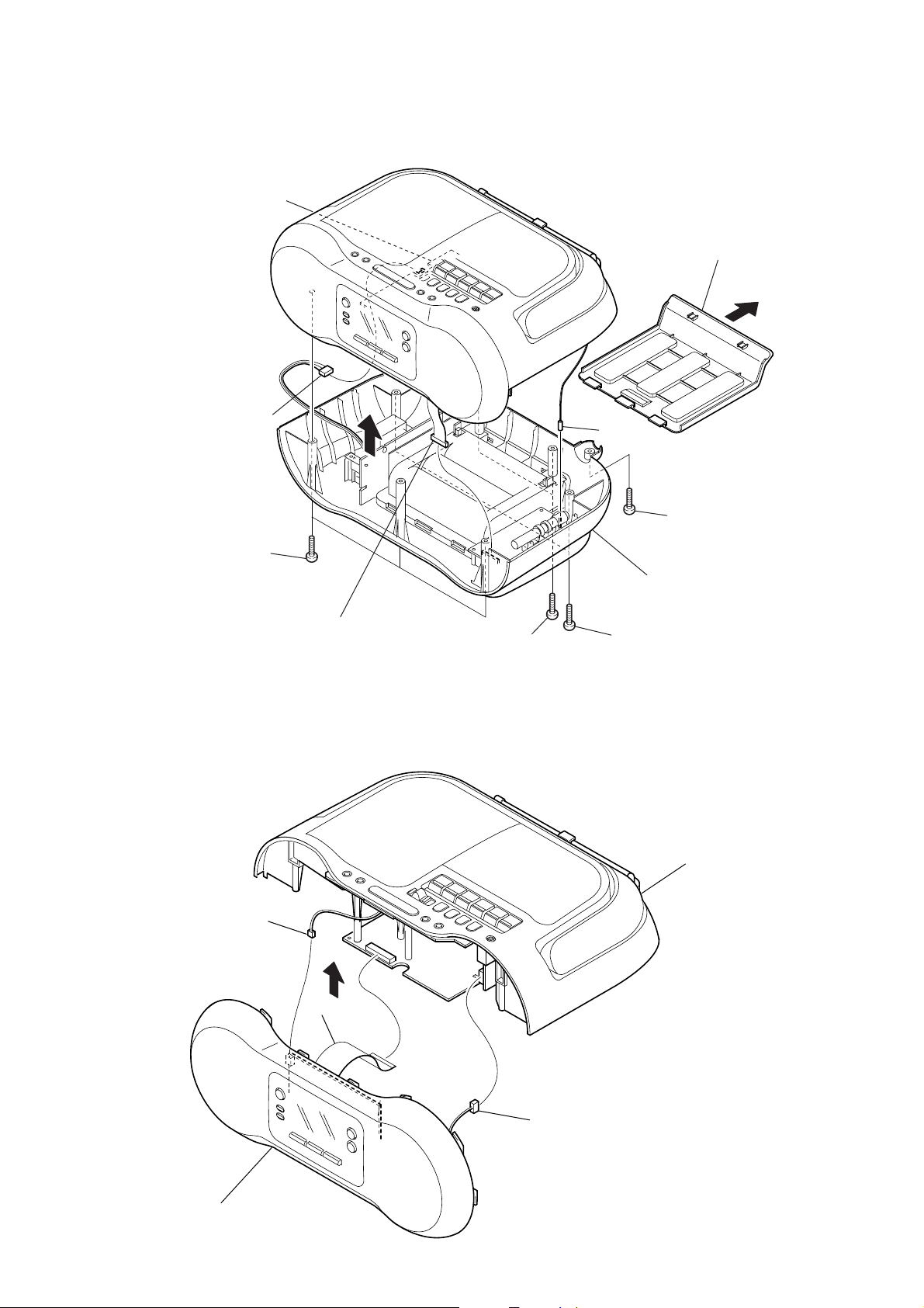
3-1. CABINET (BOTTOM) ASSY
(Page 15)
3-2. CABINET (TOP) ASSY,
CABINET (FRONT) ASSY
(Page 15)
SET
3-3. LCD BOARD,
LIGHT BOARD
(Page 16)
3-14. CD BLOCK ASSY
(Page 21)
3-4. BUTTON (PRESET)
(Page 16)
3-5. TRANSFORMER BOARD
(Page 17)
3-6. TUNER BOARD
(Page 17)
3-17. OPTICAL PICK-UP
(Page 23)
3-7. MAIN BOARD, H/P BOARD
(Page 18)
3-9. MD BLOCK ASSY
(Page 19)
3-11. TC BOARD
(Page 20)
3-16. CD BOARD
(Page 22)
3-10. CASSETTE LID
(Page 19)
3-13. M801, BELT
(Page 21)
3-15. CD LID
(Page 22)
3-8. KEY BOARD
(Page 18)
3-12. HRP301, HE301,
PINCH ROLLER ARM ASSY
(Page 20)
15
CSD-A500
3-2. CABINET (TOP) ASSY, CABINET (FRONT) ASSY
3-1. CABINET (BOTTOM) ASSY
Note : Follow the disassembly procedure in the numerical order given.
MAIN board
3
two
screws
(2.6)
0
cabinet (bottom) assy
4
two
screws
(2.6)
5
three
screws
(2.6)
7
CNP1
8
CNP901
9
CNP2
6
2
screw
(2.6)
1
battery case li
d
3
CNP403
2
CNP203
6
cabinet (top) ass
y
5
cabinet (front) assy
4
CNP804
1
16
CSD-A500
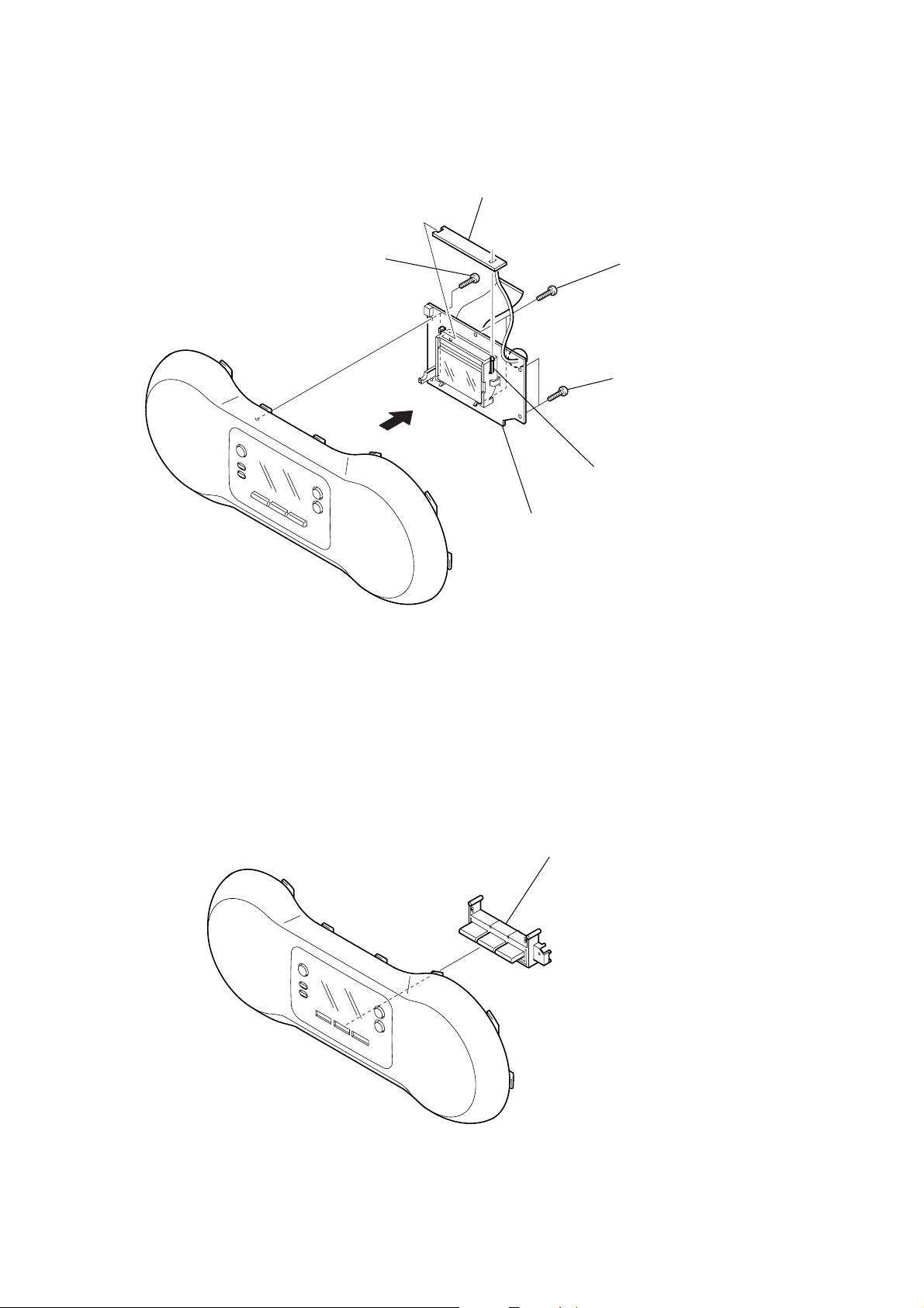
3-4. BUTTON (PRESET)
3-3. LCD BOARD, LIGHT BOARD
5
LIGHT board
6
LCD board
claw
4
1
two
screws
(+
BVTP 2.6 x 10
)
3
two
screws
(+
BVTP 2.6 x 10
)
2
two
screws
(+
BVTP 2.6 x 10
)
1
button (PRESET
)
17
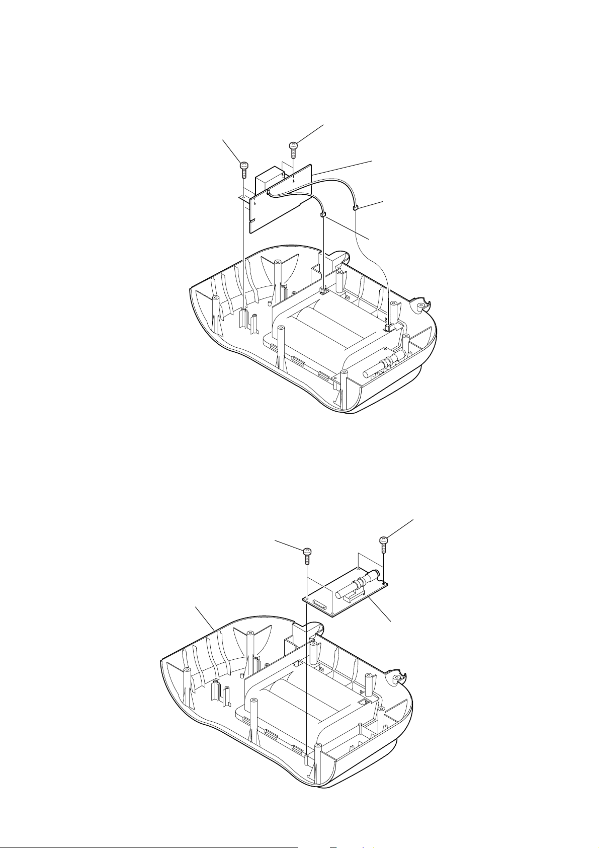
CSD-A500
3-6. TUNER BOARD
3-5. TRANSFORMER BOARD
1
CNP102
2
CNP103
5
TRANSFORMER boar
d
3
two
screws
(+
BVTP 2.6 x 10
)
4
two
screws
(+
BVTP 2.6 x 10
)
3
TUNER board
cabinet (bottom)
2
two
screws
(+
BVTP 2.6 x 10
)
1
two
screws
(+
BVTP 2.6 x 10
)
18
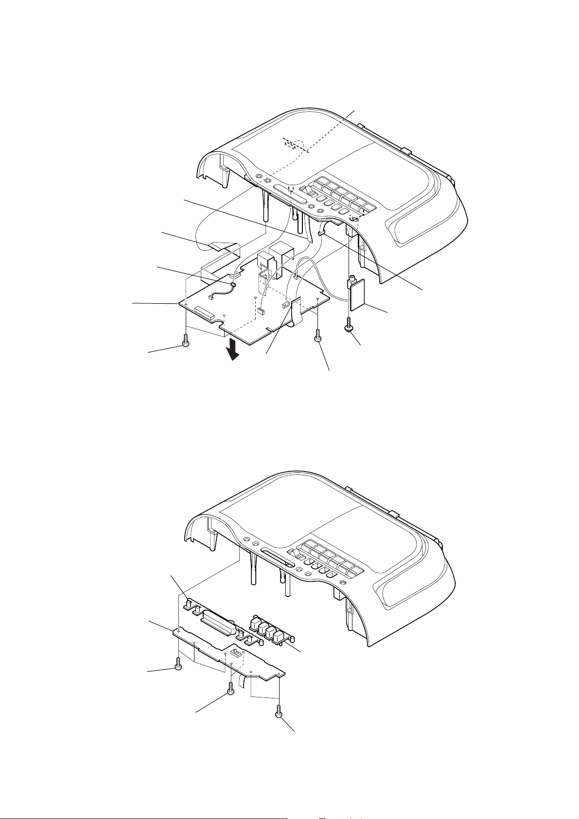
CSD-A500
3-8. KEY BOARD
3-7. MAIN BOARD, H/P BOARD
3
CNP702
8
CN303
7
0
CNP803
2
H/P board
4
connector
9
CNP805
CD board
6
two
screws
(+
BVTP 2.6 x 10
)
5
three
screws
(+
BVTP 2.6 x 10
)
qa
MAIN board
1
screw
(+
PWH 2.6 x 10
)
3
three
screws
(+
BVTP 2.6 x 10
)
2
two
screws
(+
BVTP 2.6 x 10
)
1
two
screws
(+
BVTP 2.6 x 10
)
4
KEY board
button (snooze)
button (CD)
19
CSD-A500
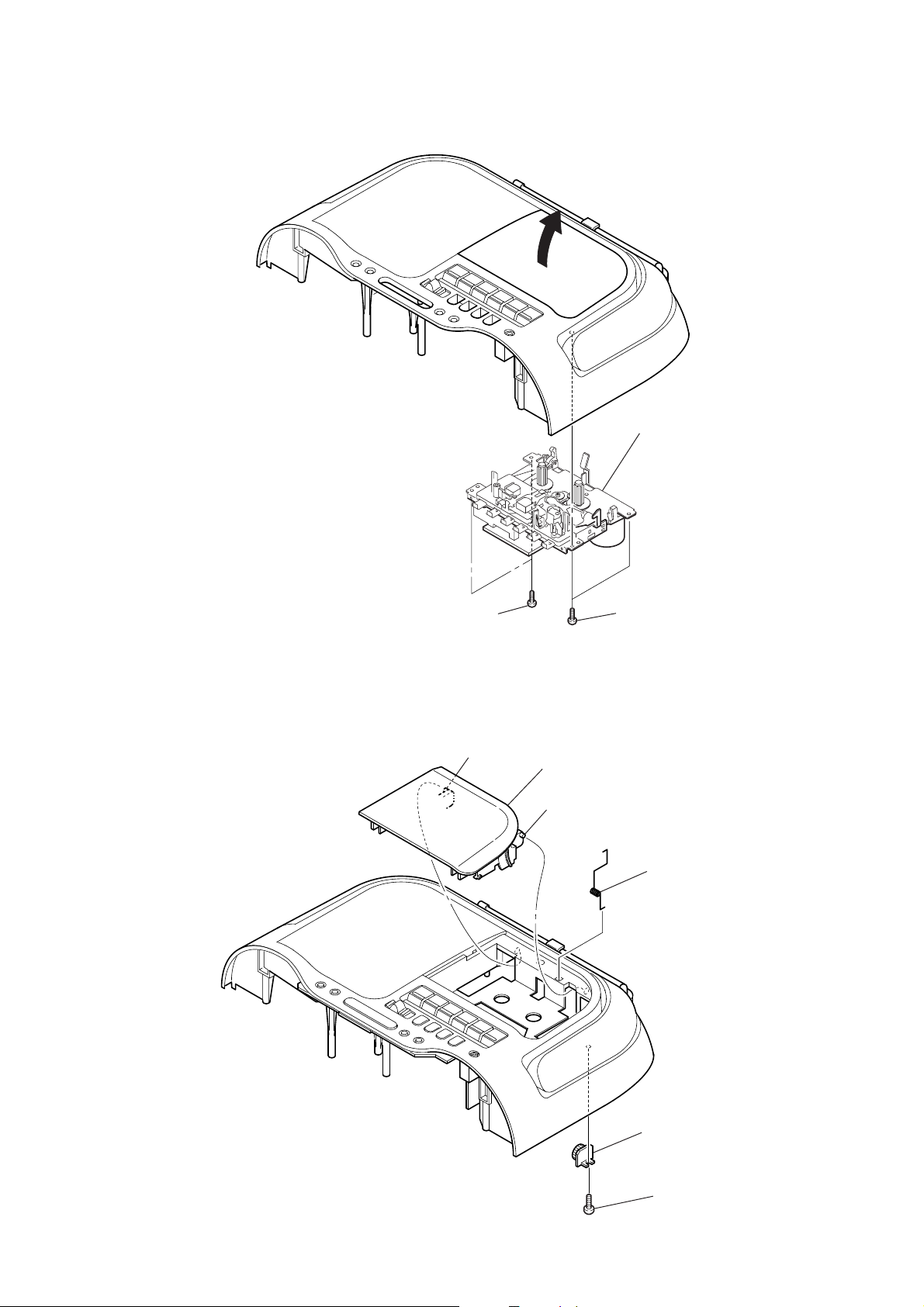
3-9. MD BLOCK ASSY
3-10. CASSETTE LID
1
screw
(+
BVTP 2.6 x 10
)
2
damper
3
cassette lid
boss
boss
4
spring (cassette)
2
two
screws
(+
BVTP 2.6 x 10
)
4
MD block assy
3
two
screws
(+
BVTP 2.6 x 10
)
1

20
CSD-A500
3-12. HRP301, HE301, PINCH ROLLER ARM ASSY
3-11. TC BOARD
1
screw
(+
BVTT 2 x 4
)
4
screw
(+
BVTT 2 x 4
)
5
TC chassis
lug
2
Remove the four soldes.
3
TC board
1
pinch roller arm ass
y
2
HE301
(ERASE head)
claw
claw
6
HRP301 (REC/PB head)
5
screw
(azimuth)
3
screw
(+B bind)
4
lug plate
7
azimuth spring
21
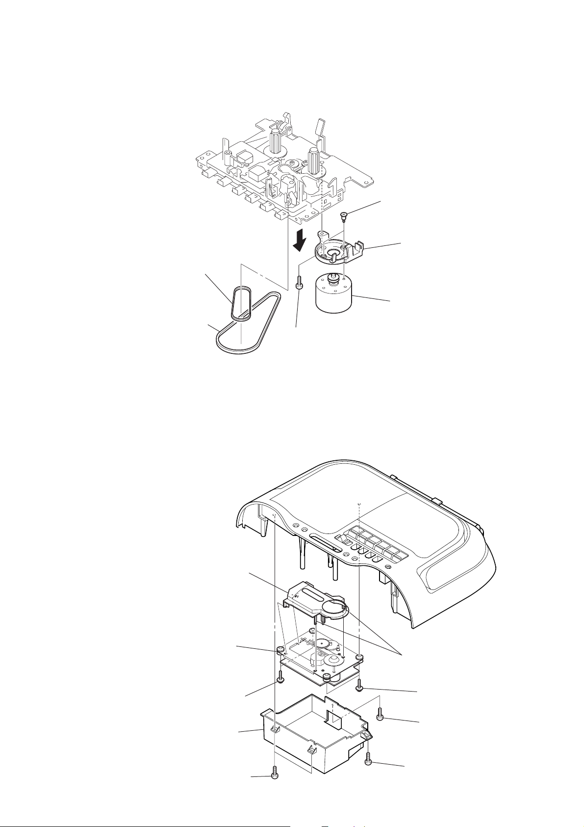
CSD-A500
3-13. M801, BEL T
3-14. CD BLOCK ASSY
1
screw (MB)
5
two
screws
(motor coller)
2
6
M801
(sub motor assy)
motor bracket
3
RF belt
4
main belt
8
CD block assy
4
cover (CD mechanical) assy
claws
7
CD cover
5
two
screws
(+
PWH (B) 2.6
)
6
two
screws
(+
PWH (B) 2.6
)
1
screw
(+
BVTP 2.6 x 10
)
2
screw
(+
BVTP 2.6 x 10
)
3
two
screws
(+
BVTP 2.6 x 10
)
Loading...