


CD-C452/C452C
SERVICE MANUAL
Illustration: CD-C452/C452C
Manufactured under license from Dolby Laboratories Licensing Corporation. DOLBY, the double-D symbol  and "PRO LOGIC" are trademarks of Dolby Laboratories Licensing Corporation.
QSOUND and the QLogo are registered trademarks of QSound Labs, Inc.
QSound is protected under US Patent Nos. 5,105,462 and 5,208,860 and foreign counterparts.
No. S4825CDC452//
CD-C452/C452C
CP-C452 Constitute CD-C452/C452C.
•In the interests of user-safety the set should be restored to its original condition and only parts identical to those specified be used.
This Service Manual is for the CD-C452/452C, which is a minor- |
|
modification model of the CD-C472. This manual, therefore, |
|
describes only the changed points from the Service manual. |
|
Please refer to the CD-C472 Service Manual (No. S2812CDC472//) |
|
together with this manual. |
|
CD-C472 |
|
|
Page |
OPERATION MANUAL .................................................... |
5 |
REMOVING AND REINSTALLING THE MAIN PARTS |
... 10 |
ADJUSTMENT ............................................................... |
12 |
TROUBLESHOOTING |
|
(CD CHANGER CONTROL / CD SECTION) ................ |
34 |
FUNCTION TABLE OF IC .............................................. |
38 |
FL DISPLAY ................................................................... |
44 |
CONTENTS |
|
|
Page |
IMPORTANT SERVICE NOTES (For U.S.A. Only) .......................................................................................................... |
2 |
SPECIFICATIONS ............................................................................................................................................................. |
2 |
NAMES OF PARTS .......................................................................................................................................................... |
3 |
QUICK GUIDE .................................................................................................................................................................. |
5 |
DISASSEMBLY ................................................................................................................................................................. |
6 |
NOTES ON SCHEMATIC DIAGRAM ............................................................................................................................... |
9 |
WAVEFORMS OF CD CIRCUIT ..................................................................................................................................... |
10 |
BLOCK DIAGRAM .......................................................................................................................................................... |
11 |
SCHEMATIC DIAGRAM / WIRING SIDE OF P.W.BOARD ............................................................................................. |
14 |
FUNCTION TABLE OF IC ................................................................................................................................................ |
28 |
REPLACEMENT PARTS LIST/EXPLODED VIEW |
|
PACKING OF THE SET (For U.S.A. Only) |
|
This document has been published to be used
SHARP CORPORATION– 1 – |
for after sales service only. |
|
|
|
The contents are subject to change without notice. |

CD-C452/C452C
FOR A COMPLETE DESCRIPTION OF THE OPERATION OF THIS UNIT, PLEASE REFER TO THE OPERATION MANUAL.
IMPORTANT SERVICE NOTES (For U.S.A.Only)
BEFORE RETURNING THE AUDIO PRODUCT
(Fire & Shock Hazard)
Before returning the audio product to the user, perform the following safety checks.
1.Inspect all lead dress to make certain that leads are not pinched or that hardware is not lodged between the chassis and other metal parts in the audio product.
2.Inspect all protective devices such as insulating materials, cabinet, terminal board, adjustment and compartment covers or shields, mechanical insulators etc.
3.To be sure that no shock hazard exists, check for leakage
current in the following manner.
*Plug the AC line cord directly into a 120 volt AC outlet.
*Using two clip leads, connect a 1.5k ohm, 10 watt resistor paralleled by a 0.15µF capacitor in series with all exposed metal cabinet parts and a known earth ground, such as conduit or electrical ground connected to earth ground.
*Use a VTVM or VOM with 1000 ohm per volt, or higher, sensitivity to measure the AC voltage drop across the resistor (See diagram).
*Connect the resistor connection to all exposed metal parts having a return path to the chassis (antenna, metal cabinet, screw heads, knobs and control shafts, escutcheon, etc.) and measure the AC voltage drop across the resistor.
VTVM
 AC SCALE
1.5k ohms
10W
0.15 µ F |
|
|
TEST PROBE |
CONNECT TO |
|
TO EXPOSED |
KNOWN EARTH |
|
METAL PARTS |
||
GROUND |
||
|
All check must be repeated with the AC line cord plug connection reversed.
Any reading of 0.3 volt RMS (this corresponds to 0.2 milliamp. AC.) or more is excessive and indicates a potential shock hazard which must be corrected before returning the audio product to the owner.
CD-C452/C452C
General
Power source: |
AC 120 V, 60 Hz |
Power consumption: |
80 W |
Dimensions: |
Width; 10-5/8" (270 mm) |
|
Height; 11-13/16" (303 mm) |
|
Depth; 13-13/16" (350 mm) |
Weight: |
13.8 lbs. (6.3 kg) |
SPECIFICATIONS
Compact disc player section
Type: |
3-disc multi-play compact disc player |
Signal readout: |
Non-contact, 3-beam semiconductor |
|
laser pickup |
D/A Converter: |
1-bit D/A converter |
Frequency response: |
20 - 20,000 Hz |
Dynamic range: |
90 dB (1 kHz) |
Amplifier section
Output power: |
FTC; 40 W minimum RMS per channel into |
(CD-C452) |
6 ohms from 60 Hz to 20 kHz with no |
|
more than 10 % total harmonic distortion. |
Output power: |
MPO; 176 W (88 W + 88 W) |
(CD-C452C) |
(10 % T.H.D.) |
|
RMS; 80 W (40 W + 40 W) |
|
(10 % T.H.D.) |
Output terminals: |
Speakers; 6 ohms |
|
Headphones; 16-50 ohms |
|
(recommended; 32 ohms) |
Input terminal: |
Video/Auxiliaary (audio signal); |
|
500 mV/47 kohms |
Tuner section
Frequency range: |
FM; 87.5 - 108 MHz |
|
AM; 530 - 1,720 kHz |
Cassette deck section
Frequency response: |
50 - 14,000 Hz (Normal tape) |
Signal/noise ratio: |
55 dB (TAPE 1, playback) |
|
50 dB (TAPE 2, recording/playback) |
Wow and flutter: |
0.15 % (WRMS) |
 Front speaker section
CP-C452
Type: |
3-way type [5-1/8" (130 mm) woofer , 2" (50 |
|
mm) tweeter and super tweeter] |
Maximum input power: |
80 W |
Impedance: |
6 ohms |
Dimensions: |
Width; 7-7/8" (200 mm) |
|
Height; 11-13/16" (300 mm) |
|
Depth; 10" (253 mm) |
Weight: |
5.9 lbs. (2.7 kg)/each |
Specifications for this model are subject to change without prior notice.
– 2 –

CD-C452/C452C
NAMES OF PARTS
CD-C452/C452C

 Front Panel
1.Disc Tray
2.Disc Number Selector Buttons
3.Disc Skip Button
4.Open/Close Button: 
5.Disc Number Indicator
6.Timer Indicator
7.Record Indicator
8.Sleep Indicator
9.Extra Bass Indicator: X-BASS 10. (CD/TUNER) Memory Indicator 11. FM Stereo Mode Indicator: ST
12.FM Stereo Indicator: 
13.(CD) Repeat Indicator: 
14.(CD) Play Indicator: 
15.(CD) Pause Indicator: 

16.Power Button
17.Dolby Pro Logic Button
18.QSOUND Button
19.Extra Bass Button: X-BASS
20.Main Volume Up/Down Buttons: 

21.Function Selector Buttons
22.Timer/Sleep Button
23.Clock Button
24.Headphone Socket
25.Tuning and Time Up/Down Buttons: 

26.Memory/Set Button
27.(TAPE) Record Pause Button: 


28.(CD) Track Down/Review Button: 

 (TUNER) Preset Down Button:
29.(CD/TAPE) Stop Button: 
30.Virtual Surround Button
31.(TAPE) Play Button:
(CD) Play/Repeat Button:
32. (CD) Track Up/Cue Button:
(TUNER) Preset Up Button:
33.Equalizer Selector/Demo Mode Button
34.(CD) Pause Button
35.(CD) Random Button
36.(CD) Clear Button
37.(TAPE 1) Cassette Compartment
38.(TAPE 2) Cassette Compartment
|
|
|
1 |
2 |
3 4 |
|
|
|
||||
|
|
|
|
|
|
|
|
|
|
|
|
|
|
|
|
|
|
|
|
|
|
|
|
|
|
|
|
|
|
|
|
|
|
|
|
|
|
|
|
|
|
|
|
|
|
|
|
|
|
|
|
|
|
|
|
|
|
|
|
|
|
|
|
|
|
|
|
|
|
|
|
|
|
|
|
|
|
5 6 7 8 9
1 2 3 |
REC SLEEP X-BASS |
13
101112
MEMORY ST |
kHz |
MHz |
14 15 |
16 17 |
18 19 |
20 |
21 |
|
|
22 |
|
35 |
23 |
|
36 |
24 |
|
|
25 |
|
|
26 27 28 29 30 |
31 32 |
33 34 |
37 38
|
Rear Panel |
|
2 |
1. |
AC Power Input Socket |
|
|
2. |
FM/AM Loop Aerial Socket |
|
|
3. |
Video/Auxiliary (Audio Signal) Input Sockets |
|
3 |
4. |
Rear Output Socket |
|
|
5. |
Center Output Socket |
|
4 |
6. |
Speaker Terminals |
1 |
|
|
|
5 |
|
|
|
|
|
|
|
|
6 |
– 3 –

CD-C452/C452C

 Speaker Section
 Front Speaker
CP-C452
1.Super Tweeter
2.Tweeter
3.Woofer
4.Bass Reflex Duct
5.Speaker Wire
CD-C452/C452C

 Remote Control
1.Remote Control Transmitter LED
2.Center Level Buttons: 

3.Dolby Pro Logic Button
4.Virtual Surround Button
5.QSOUND Buton
6.Test Tone Button
7.Balance Control Buttons: 


8.Surround Level Buttons: 

 Tuner control section
9. Preset Up/Down Buttons: 

 CD Control section
10.Disc Skip Button
11.Play/Repeat Button: 
12.Memory Button
13.Clear Button
14.Pause Button: 

15.Track Down/Review Button: 

16.Track Up/Cue Button: 


17.Stop Button: 
18.Random Button
Left speaker |
Right speaker |
|
1 |
|
2 |
|
3 |
|
4 |
|
5 |
|
1 |
|
|
2 |
|
|
|
8 |
|
|
|
3 |
|
|
|
||
|
|
|
|
|
|
||
|
|
4 |
|
|
|
9 |
|
|
|
|
|
|
|
||
Tape control section |
5 |
|
|
|
|
||
19. |
(TAPE 1) Play Button: |
|
|
|
|
||
|
|
|
|
|
|||
20. |
(TAPE 1/2) Stop Button: |
6 |
|
|
|
|
|
21. |
(TAPE 2) Play Button: |
|
|
|
|
10 |
|
22. |
(TAPE 2) Record Pause Button: |
7 |
|
|
|
||
|
|
|
|
||||
23. |
(TAPE 2) Rewind Button: |
|
|
|
11 |
||
|
|
|
|
||||
24. |
(TAPE 2) Fast Forward Button: |
12 |
|
|
|
|
|
|
|
|
|
|
|
||
Common section |
13 |
14 15 16 |
17 |
18 |
|||
25. |
Equalizer Mode Button |
||||||
|
|
|
|
|
|||
26. |
Function Selector Buttons |
19 20 |
21 22 |
||||
27. |
Power Button |
||||||
28. |
Extra Bass Button: X-BASS |
|
|
|
|
23 |
|
29. |
Volume Up/Down Buttons: |
25 |
|
|
|
||
|
|
|
|
||||
|
|
|
|
|
24 |
||
|
|
|
|
|
|
||
26 27 


 29
29
28
– 4 –

– 5 –
|
|
MINI COMPONENT |
Quick-Guide |
|
|
|
SYSTEM |
|
Guía rápida |
Preparation for use |
|
|
|
|
Preparación para su uso |
|
|
|
|
|
|
● AM Loop Antenna |
|
|
● FM Antenna |
|
● Antena de cuadro de AM |
|
|
● Antena de FM |
|
|
|
|
ANTENNA |
FM |
|
|
|
AM |
|
|
|
|
|
LOOP |
|
|
|
|
|
Red |
SPEAKERS |
Red |
|
|
Rojo |
RIGHT LEFT |
Rojo |
● AC 120 V, 60 Hz |
|
|
|
Black |
● 120 V de CA, 60 Hz |
|
|
RATED SPEAKER IMPEDANCE: |
|
|
|
6 OHMS MIN. |
Negro |
|
|
|
Black |
|
|
|
|
|
|
|
|
|
Negro |
|
|
Turning the power on and off |
|
Sound control |
||
Conexión y desconexión de la alimentación |
Control del sonido |
|||
|
|
|
● Volume |
|
POWER |
|
|
● Volumen |
|
|
|
|
||
|
|
|
VOLUME |
|
|
|
|
UP • • • |
|
|
|
|
|
VOLUME |
|
|
|
X-BASS |
|
|
POWER |
|
|
|
|
|
|
DOWN • |
|
Remote control
Control remoto
+ |
|
● 2 "AA" batteries |
- |
+ |
● Dos pilas "AA" |
|
- |
|
|
|
|
|
|
● Batteries are not |
|
|
included. |
|
|
● Las pilas no |
|
|
están incluidas. |
●Equalizer
●Ecualizador
|
|
EQUALIZER |
|
|
|
|
|
|
EQUALIZER |
Remote Sensor |
|
|
MODE |
|
Sensor remote |
DEMO |
|
|
|
|
|
FLAT |
HEAVY-1 |
HEAVY-2 |
|
|
SOFT-2 |
SOFT-1 |
VOCAL |
|
|
● Extra-BASS |
|
|
8" - 20' (0.2m - 6m) |
● Graves extra |
|
||
|
|
|
||
0,2m - 6m |
|
VOLUME |
|
|
|
|
UP • • • |
|
X-BASS |
|
15 |
|
|
|
15 |
|
|
|
|
|
|
X-BASS |
|
|
|
|
DOWN • |
|
|
CD playback
Reproducción de discos compactos
C D |
OPEN |
OPEN |
|
|
 ● Label facing up
● Etiqueta hacia arriba
Tape playback
Reproducción de cintas
TAPE |
|
|
(1 |
2) |
|
|
TAPE 1 |
TAPE 2 |
Radio operation
Funcionamiento de la radio
FM STERO |
FM MONO |
AM |
|
ST |
|
TUNER |
|
|
(BAND) |
|
|
|
|
TUNING/TIME |
Recording from CDs
Grabación de discos compactos
REC PAUSE 

C D
TAPE 2 |
|
● Load the disc to be recorded. |
● CD recording starts. |
● Introduzca el disco que va a grabar. |
● La grabación de CD empieza. |
Precaution
Precaución
● The sound level at a given volume setting |
● El nivel de sonido en una posición de volumen |
depends on a combination of speaker effi- |
fijado depende de una combinación del rendi- |
ciency, location and many other factors. It is |
miento de las altavoces, la posición y muchos |
advisable to avoid exposure to high volume |
otros factores. Es aconsejable evitar un aumen- |
levels, which occur while turning the unit on |
to de volumen. Esto se produce, por ejemplo, |
with the volume control setting up high, or |
al conectar el aparato con el volumen puesto |
while continually listening at high volume le- |
en una posición alta. Evite continuar la audición |
vels. |
prolongada a altos niveles de sonido. |
● Only discs bearing the logo as shown can |
● En este aparato sólo pueden reproducirse los |
be played in this unit. |
discos que tengan el logotipo mostrado. |
C452/C452C-CD
CD-C452/C452C
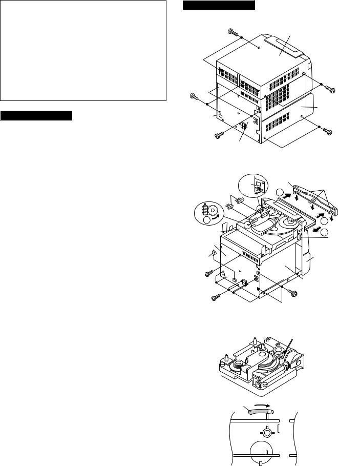
DISASSEMBLY
Caution on Disassembly
Follow the below-mentioned notes when disassembling the unit and reassembling it, to keep it safe and ensure excellent performance:
1.Take cassette tape and compact disc out of the unit.
2.Be sure to remove the power supply plug from the wall outlet before starting to disassemble the unit.
3.Take off nylon bands or wire holders where they need to be removed when disassembling the unit. After servicing the unit, be sure to rearrange the leads where they were before disassembling.
4.Take suffcient care on static electricity of integrated circuits and other circuits when servicing.
CD-C452/C452C
STEP |
REMOVAL |
|
PROCEDURE |
|
FIGURE |
|
|
|
|
|
|
1 |
Top Cabinet |
1. |
Screw ..................... |
(A1) x4 |
6-1 |
|
|
|
|
|
|
2 |
Side Panel |
1. |
Screw ..................... |
(B1) x6 |
6-1 |
|
(Left/Right) |
|
|
|
|
|
|
|
|
|
|
3 |
CD Player Unit/ |
1. |
Turn on the power supply, |
6-2 |
|
|
CD Tray Cover |
|
open the disc tray, take out |
|
|
|
|
|
the CD cover, and close. |
|
|
|
|
|
(Note 1) |
|
|
|
|
2. |
Hook ....................... |
(C1) x3 |
|
|
|
3. |
Hook ....................... |
(C2) x2 |
|
|
|
4. |
Screw ..................... |
(C3) x1 |
|
|
|
5. |
Socket .................... |
(C4) x2 |
|
|
|
|
|
|
|
4 |
Back Board |
1. |
Screw ..................... |
(D1) x9 |
6-2 |
|
|
2. |
Socke ..................... |
(D2) x1 |
|
|
|
|
|
|
|
5 |
Main PWB |
1. |
Screw ..................... |
(E1) x1 |
7-1 |
|
|
2. |
Socket .................... |
(E2) x2 |
|
|
|
3. |
Flat Wire ................. |
(E3) x1 |
|
|
|
4. |
Tip Wire .................. |
(E4) x1 |
|
|
|
5. |
Socket .................... |
(E5) x1 |
|
|
|
|
|
|
|
6 |
Front Panel |
1. |
Screw ..................... |
(F1) x2 |
7-1 |
7 |
Display PWB/ |
1. |
Socket .................... |
(G1) x1 |
7-2 |
|
Switch PWB |
2. |
Screw ..................... |
(G2) x11 |
|
|
|
|
|
|
|
8 |
Tape Mechanism |
1. |
Open the cassette holder. |
7-2 |
|
|
|
2. |
Screw...................... |
(H1) x5 |
|
9 |
Power Amp. PWB |
1. |
Screw ..................... |
(J1) x3 |
7-3 |
|
|
2. |
Socket .................... |
(J2) x2 |
|
|
|
|
|
|
|
10 |
Turntable |
1. |
Screw ..................... |
(K1) x1 |
7-4 |
|
|
2. |
Cover ..................... |
(K2) x1 |
|
11 |
CD Player Base |
1. Screw ..................... |
(L1) x2 |
7-4 |
|
|
|
2. |
Guide ..................... |
(L2) x2 |
|
|
|
|
|
|
|
12 |
CD Servo PWB |
1. |
Screw ..................... |
(M1) x1 |
7-5 |
|
|
2. |
Socket .................... |
(M2) x4 |
|
13 |
CD Changer |
1. |
Screw ..................... |
(N1) x4 |
7-6 |
|
Mechanism |
|
|
|
|
|
|
|
|
|
|
14 |
CD Mechanism |
1. |
Screw ..................... |
(P1) x1 |
7-6 |
|
|
|
|
|
|
Note 1:
How to open the changer manually. (Fig. 6-3)
1.Insert the tip of fine screwdriver into the hole of CD player base, and press down the worm wheel < A > .
2.Then, turn fully the lock lever in the arrow direction through the hole on the loading chassis bottom in this state.
After that, push forward the CD player base.
CD-C452/C452C
( A1 ) x2 |
Top Cabinet |
ø3 x12mm |
|
|
|
|
|
( A1 ) x2 |
( B1 ) x2 |
|
|
|
ø3 x12mm |
|
|
|
|
|
ø3 x8mm |
|
|
|
|
|
|
|
|
Side Panel |
Side Panel |
|
|
|
(Left) |
(Right) |
|
|
|
|
( B1 ) x2 |
|
|
|
( B1 ) x2 |
ø3 x8mm |
Back Board |
|
||
|
|
ø3 x8mm |
||
|
|
Figure 6-1 |
|
|
|
|
(C2) x1 |
CD Tray Cover |
Hook |
|
|
|
( C1) x3 |
|
( C4 ) x2 |
Pull |
|
||
1 |
|
|||
|
|
|||
A |
|
|
|
1 |
CD Player Unit |
|
|
|
2 |
Back Board |
|
|
|
( C2 ) x1 |
|
|
|
|
|
( D2 ) x1 |
|
|
|
Front Panel |
|
|
|
|
|
( C3 ) x1 |
|
|
Main PWB |
|
ø3 x8mm |
|
|
|
|
( D1 ) x7
( D1 ) x2
ø3 x8mm
ø3 x10mm
Figure 6-2
< A >
LOCK
LEVER
Figure 6-3
– 6 –

Front Panel
( E4 ) x1
( E2 ) x2
( E3 ) x1 |
Push |
|
|
|
|
||
Power Amp. |
|
Tape |
|
PWB |
|
||
Push |
Mechanism |
||
|
|||
|
|
( E1 ) x1 |
|
|
|
ø3 x10mm |
|
Main PWB |
( F1 ) x2 |
|
|
|
ø3 x8mm |
|
|
|
(E5) x1 |
|
Figure 7-1
|
Switch PWB |
|
|
Front Panel |
|
( G2 ) x3 |
|
|
ø3 x10mm |
|
( G1 ) x1 |
|
|
|
( G2 ) x8 |
|
Display |
ø3 x10mm |
|
PWB |
|
|
Open |
( H1 ) x5 |
|
|
ø3 x10mm |
|
|
|
Tape |
Cassette |
|
Mechanism |
|
|
Holder |
|
|
|
|
|
|
(Left/Right) |
|
Figure 7-2 |
|
|
( J1 ) x3 |
|
Power |
ø3 x12mm |
|
( J2 ) x1 |
||
Transformer |
||
|
||
( J2 ) x1 |
|
Power Amp.
PWB
Figure 7-3
CD-C452/C452C
( K1 ) x1 ø3 x10mm 
( K2 ) x1
Washer
Turntable
( L1 ) x1 |
CD Player Base |
|
|
ø3 x10mm |
|
( L2 ) x1 |
|
|
( L1 ) x1 |
|
ø3 x10mm |
Loading chassis |
( L2 ) x1 |
|
|
|
Figure 7-4 |
( M1 ) x1  ø3 x10mm

 CD Servo PWB ( M2 ) x2
( M2 ) x2
Loading chassis
Figure 7-5
 ( N1 ) x4
 ø3 x12mm
( P1 ) x1 ø2.6 x10mm
Shift Lever
CD Changer
Mechanism
CD Player Base |
CD Mechanism |
Be careful when installing the CD changer mechanism. Install the CD changer mechanism on the CD player base after the shift lever has been set in the highest position.
Figure 7-6
– 7 –

CD-C452/C452C
CP-C452
STEP |
REMOVAL |
|
PROCEDURE |
|
FIGURE |
|
|
|
|
|
|
1 |
Front Speaker |
1. Net .......................... |
(A1) x1 |
8-1 |
|
|
|
2. |
Baffle Board ........... |
(A2) x1 |
|
|
|
3. |
Screw ..................... |
(A3) x2 |
8-2 |
|
|
4. Screw ..................... |
(A4) x4 |
|
|
|
|
5. Screw ..................... |
(A5) x2 |
|
|
|
|
|
|
|
|
Note:
The center and rear speakers can be easily disassembled. Therefore the disassembling method is not discribed.
For details refer to the disassembling drawing in the Parts Guide.
CP-C452
Tweeter
Baffle Board ( A2 ) x1
Net
( A1 ) x1
Woofer
Screwdriver
Figure 8-1
Super
Tweeter
( A5 ) x2
ø3 x10mm
Tweeter
( A3 ) x2 ø3 x10mm
( A4 ) x4 ø4 x14mm
Woofer
Figure 8-2
– 8 –

CD-C452/C452C
NOTES ON SCHEMATIC DIAGRAM
∙Resistor:
To differentiate the units of resistors, such symbol as K and M are used: the symbol K means 1000 ohm and the symbol M means 1000 kohm and the resistor without any symbol is ohm-type resistor. Besides, the one with “Fusible” is a fuse type.
∙Capacitor:
To indicate the unit of capacitor, a symbol P is used: this symbol P means micro-micro-farad and the unit of the capacitor without such a symbol is microfarad. As to electrolytic capacitor, the expression “capacitance/withstand voltage” is used.
(CH), (TH), (RH), (UJ): Temperature compensation (ML): Mylar type
(P.P.): Polypropylene type
∙Schematic diagram and Wiring Side of P.W.Board for this model are subject to change for improvement without prior notice.
∙The indicated voltage in each section is the one measured by Digital Multimeter between such a section and the chassis with no signal given.
1.In the tuner section, ( ) indicates AM
< > indicates FM stereo
2.In the main section, a tape is being played back.
3.In the deck section, a tape is being played back. ( ) indicates the record state.
4.In the power section, a tape is being played back.
5.In the CD section, the CD is stopped.
∙Parts marked with “ ” (
” ( 


 ) are important for maintaining the safety of the set. Be sure to replace these parts with specified ones for maintaining the safety and performance of the set.
REF. NO |
DESCRIPTION |
POSITION |
|
|
|
SW1 |
OPEN/CLOSE |
ON—OFF |
|
|
|
SW2 |
MECHA UP |
ON—OFF |
|
|
|
SW3 |
DISC NUMBER |
ON—OFF |
|
|
|
SW4 |
PICKUP IN |
ON—OFF |
SW701 |
EQUALIZER/DEMO |
ON—OFF |
|
|
|
SW702 |
VOLUME DOWN |
ON—OFF |
|
|
|
SW703 |
X-BASS |
ON—OFF |
|
|
|
SW704 |
VOLUME UP |
ON—OFF |
|
|
|
SW705 |
OPEN/CLOSE |
ON—OFF |
|
|
|
SW706 |
DISC SKIP |
ON—OFF |
|
|
|
SW707 |
DISC 1 |
ON—OFF |
|
|
|
SW708 |
DISC 2 |
ON—OFF |
|
|
|
SW709 |
DISC 3 |
ON—OFF |
|
|
|
SW710 |
REC/PAUSE |
ON—OFF |
|
|
|
SW711 |
PRESET UP |
ON—OFF |
|
|
|
SW712 |
STOP |
ON—OFF |
|
|
|
SW713 |
PLAY/REPEAT |
ON—OFF |
|
|
|
SW714 |
PRESET DOWN |
ON—OFF |
|
|
|
SW715 |
TUNING UP |
ON—OFF |
|
|
|
REF. NO |
DESCRIPTION |
POSITION |
|
|
|
SW716 |
TUNING DOWN |
ON—OFF |
|
|
|
SW717 |
POWER |
ON—OFF |
SW718 |
CLOCK |
ON—OFF |
|
|
|
SW719 |
TIMER/SLEEP |
ON—OFF |
|
|
|
SW720 |
MEMORY/SET |
ON—OFF |
|
|
|
SW721 |
CD |
ON—OFF |
|
|
|
SW722 |
TUNER/BAND |
ON—OFF |
|
|
|
SW723 |
TAPE |
ON—OFF |
SW724 |
VIDEO/AUX |
ON—OFF |
|
|
|
SW725 |
PRO LOGIC |
ON—OFF |
|
|
|
SW726 |
VIRTUAL |
ON—OFF |
|
|
|
SW727 |
Q-SOUND |
ON—OFF |
|
|
|
SW728 |
CD PAUSE |
ON—OFF |
|
|
|
SW729 |
CD CLEAR |
ON—OFF |
SW730 |
RANDOM |
ON—OFF |
|
|
|
SWM 3 |
FOOL PROOF |
ON—OFF |
|
|
|
SWM 4 |
F.A.S. |
ON—OFF |
|
|
|
SWM 5 |
CAM |
ON—OFF |
|
|
|
|
|
FRONT |
|
|
|
|
|
|
|
|
|
|
|
|
|
|
|
|
|
|
|
|
|
|
||||||
|
|
|
|
|
|
|
|
|
|
|
|
|
|
|
|
|
|
|
|
|
|
|
|
|||||||
|
|
|
VIEW |
|
|
FRONT |
|
|
|
|
|
|
|
|
|
|
|
|
|
|||||||||||
|
|
|
|
|
|
|
|
|
|
|
|
VIEW |
|
|
|
|
|
|
|
|
|
|
|
|
|
|||||
|
|
|
|
|
|
|
|
|
|
|
|
|
|
|
|
|
|
|
|
|||||||||||
|
|
|
|
|
|
|
|
|
|
|
|
|
|
|
|
|
|
|
|
|
|
|
|
|
|
|
|
|
|
|
|
|
|
|
|
|
|
|
|
|
|
|
|
|
|
|
|
|
|
|
|
|
|
|
FRONT |
||||||
|
|
|
|
|
|
|
|
|
|
|
|
|
|
|
|
|
|
|
|
|
|
|
|
|
|
|
VIEW |
|||
|
|
E C B |
|
|
|
|
|
|
|
|
|
|
|
|||||||||||||||||
|
|
|
|
|
|
|
|
|
|
|
|
|
|
|
|
|
|
|
|
|
|
|
||||||||
|
(S) (G)(D) |
|
B C E |
|
|
|
|
|
|
|
|
|
|
|||||||||||||||||
|
|
|
|
|
|
|
|
|
|
|
|
|||||||||||||||||||
|
(1) (2) (3) |
|
|
|
|
|
|
|
|
|
|
|
|
|
|
|
|
|
|
|
|
|
||||||||
2SA1015 GR |
KRC107 M |
2SD2012 |
333YTH2 |
|||||||||||||||||||||||||||
2SC535 |
C |
KTA1266 GR |
KTA1273 Y |
|
|
|
|
|
|
|
|
|
|
|||||||||||||||||
2SD468 |
C |
KTA1268 GR |
|
|
|
|
|
|
|
|
|
|
|
|
|
|
|
|
|
|
|
|
|
|||||||
KRA102 M |
KTA1271 Y |
|
|
|
|
|
|
|
|
|
|
|
|
|
|
|
|
|
|
|
|
|
||||||||
KRA109 M |
KTC3199 GR |
|
|
|
|
|
|
|
|
|
|
|
|
|
|
|
|
|
|
|
|
|
||||||||
KRC102 M |
KTC3200 GR |
|
|
|
|
|
|
|
|
|
|
|
|
|
|
|
|
|
|
|
|
|
||||||||
KRC104 M |
KTC3203 Y |
|
|
|
|
|
|
|
|
|
|
|
|
|
|
|
|
|
|
|
|
|
||||||||
Figure 9 TYPES OF TRANSISTOR AND LED
– 9 –
CD-C452/C452C
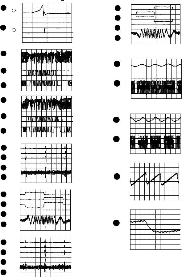
WAVEFORMS OF CD CIRCUIT
STOP  PLAY
PLAY
FOCUS SERCH
1 |
5ms |
|
|
|
0.50 V |
F.E |
|
||
|
IC1 20 |
|
||
2 |
5ms |
|
|
|
5.0 V |
DRF |
|
||
|
IC1 54 |
3 |
||
|
|
|
||
|
|
|
1 |
|
3 |
0.5ms |
CUE |
||
|
||||
1.00 V |
|
|||
|
HF |
|
||
4 |
0.5ms |
1 |
||
5.0 V |
2 |
|||
|
HFL |
|||
|
|
|||
5 |
0.5ms |
3 |
||
|
||||
5.0 V |
|
|||
|
|
|||
|
TES |
|
||
3 |
0.5ms |
REVIEW |
||
1.00 V |
|
|||
|
HF |
|
||
4 |
0.5ms |
1 |
||
5.0 V |
2 |
|||
|
HFL |
|||
5 |
0.5ms |
3 |
||
5.0 V |
|
|||
|
|
|||
|
TES |
|
||
6 |
50ms |
CUE |
||
10.0 V |
||||
|
||||
|
JP+ |
|
||
7 |
50ms |
|
||
10.0 V |
|
|||
|
JP- |
|
|
|
8 |
50ms |
|
||
0.50 V |
|
|||
|
JP |
|
|
|
9 |
50ms |
|
||
1.00 V |
|
|||
|
TE |
|
|
|
6 |
0.5ms |
|
||
10.0 V |
|
|||
|
JP+ |
|
|
|
7 |
0.5ms |
|
||
10.0 V |
|
|||
|
JP- |
|
|
|
8 |
0.5ms |
|
||
0.50 V |
|
|||
|
JP |
|
|
|
9 |
0.5ms |
|
||
1.00 V |
|
|||
|
TE |
|
|
|
6 |
50ms |
REVIEW |
||
10.0 V |
||||
|
||||
|
JP+ |
|
|
|
7 |
50ms |
|
||
10.0 V |
|
|||
JP- |
|
|
||
|
|
|
||
8 |
50ms |
|
||
0.50 V |
|
|||
|
JP |
|
|
|
9 |
50ms |
|
||
1.00 V |
|
|||
TE |
|
|
||
|
|
|
||
6 |
0.5ms |
10.0 V |
|
|
JP+ |
7 |
0.5ms |
10.0 V |
|
|
JP- |
8 |
0.5ms |
0.50 V |
|
|
JP |
9 |
0.5ms |
1.00 V |
|
|
TE |
|
PLAY |
|
NORMAL DISC |
|
TN0=01 |
10 |
20ms |
1.00 V |
|
|
SPO |
11 |
20ms |
2.00 V |
|
|
CLV+ |
|
PLAY |
|
TCD-712 (140mm) |
|
TN0=01 |
10 |
50ms |
1.00 V |
|
|
SPO |
11 |
50ms |
2.00 V |
|
|
CLV+ |
|
PLAY |
|
TCD-712 |
12 |
5s |
100mV |
|
|
SLD |
|
1 |
12 100mV0.5s |
|
|
SLD |
|
1 |
– 10 –
11 – |
BLOCK 11 Figure |
– |
DIAGRAM |
|
(1/3) |
|
PICKUP UNIT |
|
|
+5V |
|
|
|
|
|
|
|
|
|
|
|
|
|
|
|
|
|
|
|
|
|
|
|
|
|
|
|
|
|
|
|
|
|
|
Q1 |
|
|
|
|
|
|
+5V |
|
|
|
|
|
|
|
|
|
|
|
|
|
|
|
XL1 |
|
|
|
|
|
|
|
|
|
|
|
|
|
|
|
|
|
|
|
|
|
|
|
|
|
|
|
|
|
|
62 |
64 |
|
|
|
45 |
44 |
6 23 36 41 43 |
|
|
CNP11 |
|
|
||
|
|
|
LD0 |
VCC1 |
|
|
|
XIN |
XOUT |
VVDD VDD LVDD |
RVDD XVDD |
|
|
|
|
||
|
|
|
|
|
|
|
|
|
|
|
|
|
|
||||
|
|
|
|
|
|
|
|
|
IC2 |
LCHO 37 |
|
|
16 |
|
|
|
|
|
|
|
|
|
|
|
|
|
LVSS 38 |
|
|
TO MAIN SECTION |
|||||
|
|
|
|
IC1 |
|
|
|
|
LC78623D |
RVSS 39 |
|
|
25 |
||||
|
|
|
|
|
|
|
|
|
|
35 |
|
|
|
||||
|
|
|
|
|
|
|
|
|
RCHO 40 |
|
|
|
( TO IC601 ) |
||||
|
|
|
LA9241M |
|
|
9 EFMO SERVO/SIGNAL |
|
|
|
|
|||||||
|
|
|
|
JP– 32 |
|
|
|
|
|
|
|||||||
|
|
|
|
|
|
|
|
|
|
|
|
|
|
|
|
|
|
|
|
1 FIN2 |
|
|
|
~ |
10 EFMIN |
|
|
|
|
|
|
|
|
||
FOCUS COIL |
2 FIN1 SERVO AMP. CV+ 40 |
12 CLV+ |
CONTROL |
|
|
|
|
|
|
|
|||||||
|
|
3 E |
|
|
|
SLC 43 |
~ |
|
|
|
|
|
|
|
|
|
|
TRACKING COIL |
4 |
F |
|
|
|
SL1 44 |
20 JP– |
|
|
CONT1 24 |
1 |
IC81 |
6 |
+B1 |
|
|
|
|
|
|
|
|
|
|
RES. CQCK. |
|
TA7291S |
|
|
||||||
|
|
|
TO FD SPO NC SLD |
SL– SL+ |
DRF |
|
DAT CE |
|
|
CONT2 25 |
9 |
LORDING MOTOR |
5 |
|
|
|
|
|
|
|
CL |
|
COIN SQOUT. |
|
|
|
|||||||||
|
|
|
|
|
|
DRIVER |
|
|
|
|
|||||||
|
|
|
|
|
|
|
|
|
|
|
|
|
|
|
|||
|
|
|
|
|
|
|
|
|
RWC. WRQ |
CONT3 |
|
|
|
|
|
|
|
|
|
|
|
|
|
|
|
|
|
|
3 7 |
|
|
|
|
||
|
|
|
15 16 27 23 29 |
30 31 54 |
51 52 53 |
|
53 ~ 58 |
26 |
|
|
|
|
|
|
|||
|
|
|
|
|
|
|
CL, DAT, SELIAL CONTROL/CE |
|
|
|
|
|
|
|
|
|
|
|
|
|
|
|
|
|
|
|
|
Q93 |
|
|
|
|
|
|
|
M2 |
M1 |
|
|
|
|
|
|
|
|
|
|
|
|
|
|
|
|
SLED |
DISC |
|
|
|
|
SL+. SL–. DRF |
|
|
|
|
|
|
10 |
GND (D) |
10 |
SW2 |
|
MOTOR |
MOTOR |
|
|
|
|
|
|
|
|
|
|
|
|
||||
|
|
|
|
|
|
|
|
|
|
|
|
9 |
MECHA UP |
9 |
MECHA UP |
||
|
|
|
|
|
|
|
|
|
|
|
|
|
|
||||
|
|
|
|
|
|
|
|
|
|
|
|
|
|
|
|||
M |
M |
|
5 22 32 |
|
|
|
|
|
|
|
|
|
|
8 |
GND (D) |
8 |
SW3 |
6 |
|
|
|
|
|
|
|
|
|
|
|
7 |
DISK NO. |
7 |
DISC No. |
||
|
|
|
|
20 |
|
+B1 |
|
|
|
|
|
|
6 |
OPEN/CLOSE |
6 |
SW1 |
|
|
|
7 |
IC3 |
|
26 |
|
|
|
|
|
|
|
|
5 |
GND (D) |
5 |
OPEN/CLOSE |
|
|
12 |
|
|
|
|
|
|
|
|
|
|
|||||
|
|
|
|
|
|
|
|
|
|
|
4 |
M– |
4 |
M3 |
|||
|
|
|
|
27 |
|
|
|
|
|
|
|
|
|
|
|
M LOADING |
|
|
|
13 |
M56748FP |
|
|
|
|
|
|
|
|
3 |
M+ |
3 |
|||
|
|
28 |
|
|
|
|
|
|
|
|
|||||||
|
|
|
|
|
|
|
|
|
|
|
|||||||
|
|
24 |
DRIVER |
29 |
|
|
|
|
|
|
|
|
2 |
GND (M) |
2 |
|
|
|
|
|
|
|
|
Q91 |
|
|
|
1 |
|
1 |
SOLM1 |
||||
|
|
25 |
|
|
34 |
|
|
|
|
|
|
|
|
||||
|
|
|
|
|
|
|
|
|
|
|
|
|
|
|
|
||
|
|
30 |
|
|
35 |
|
|
|
|
|
|
|
CNP10 |
CNS10 |
|
||
|
|
31 |
|
|
36 |
|
|
|
|
|
|
|
|
|
|
|
|
PICKUP IN |
8 9 10 11 |
SW4 |
|
PU-IN SW |
|
|
TO DISPLAY |
|
|
|
SECTION |
|
|
6 |
+12V (+B5) |
+5V |
Q52 |
5 |
+7.3V (+B1) |
|
REGULATOR |
CNP11 |
|
+7.3V |
|
|
|
C452/C452C-CD

CD-C452/C452C
FM&AM LOOP ANT
FM BPF |
|
|
IC301 |
|
|
FM IF |
|
||
|
|
|
|
|
|
|
|
||
BF301 |
1 |
FM FRONT END |
|
6 |
T301 |
CF301 |
|||
|
|
|
TA7358AP |
|
|
|
|
||
|
2 |
3 |
4 |
|
|
8 |
9 |
|
|
|
5 |
7 |
|
|
|
||||
|
|
|
|
FM |
OSC |
|
|
|
|
|
|
L302 |
|
FM RF |
|
L303 |
FM OSC |
|
|
|
|
|
|
|
|
Q302 |
|
|
|
|
|
|
|
|
OSC BUFF |
|
|
||
|
AM TRACKING |
|
|
|
|
|
|
|
|
|
|
|
|
|
|
|
|
|
AM BAND |
|
|
|
|
|
|
|
|
|
COVERAGE |
T302
AM ANT.
FM +B
|
|
+B4 |
|
+B4 |
|
|
|
|
|
|
|
|
|
|
|
|
VR351 |
|
|
|
AM IF |
|
|
|
MPX VCO ADJ |
|
|||
|
|
T351 |
|
|
T352 |
|
|
MONO/ST |
|
FM IF IN |
|
|
|
|
|
|
|||
|
|
|
|
|
FM DET |
|
|
||
|
|
|
|
|
|
|
|
||
1 |
3 |
|
5 |
6 |
21 |
20 |
13 |
15 |
|
|
AM MIX |
AM IF |
GND FM+B |
FM DET |
VCO MO/ST |
|
|||
|
|
|
FM/AM IF |
|
|
|
L 9 |
|
|
|
|
|
IC303 |
|
|
|
MPX IN |
R 10 |
|
|
|
|
LA1805 |
|
DET OUT |
|
FM/AM |
|
|
|
24 |
23 |
22 |
|
7 |
17 |
16 |
11 |
|
|
INOSCAM |
AM+B |
INRFAM |
|
STEREO |
|
|
FM/AM |
|
|
|
|
|
|
|
|
|
SWITCHING |
|
FM OSC |
|
|
|
|
|
|
|
Q343 |
FM |
|
|
|
|
|
|
|
|
|
|
|
|
X352 |
|
|
|
|
|
|
|
VOLTAGE |
|
|
|
|
|
|
|
|
|
REGURATER |
|
|
4.5MHz |
IN |
|
IN |
|
|
|
|
|
|
VT |
|
|
|
|
|
|
|
+B4 |
||
|
|
AM |
|
FM |
CE |
|
DI CL |
DO |
||
|
1 |
|
|
4 |
|
|||||
20 |
22 |
15 |
16 |
11 |
3 |
5 |
6 |
|
||
|
|
OSC |
IC302 |
|
|
|
|
LC72131 |
17 |
|
|
PLL CONTROLLER |
||
SWITCHING |
|
|
||
7 |
10 |
|
21 |
|
Q344 |
FM |
ST |
|
|
|
|
|
|
|
|
|
|
|
ST FM |
|
|
|
|
|
|
|
|
|
|
|
|
|
|
|
JK601 |
CL |
|
|
|
|
|
|
|
|
|
|
|
|
|
|
|
|
2 |
||
|
|
|
|
|
|
|
|
|
|
|
|
|
|
|
VIDEO/AUX |
||
|
|
|
|
|
|
|
|
|
|
|
|
|
|
|
|
||
|
|
|
|
|
|
|
|
|
|
|
|
|
|
|
L |
AUX |
L 52 |
|
|
|
|
|
|
|
|
|
|
|
|
|
|
|
R |
|
R 60 |
|
CNS11 |
|
|
|
|
|
|
|
|
|
|
|
|
|
|
TAPE |
L 53 |
|
|
|
|
|
|
|
|
|
|
|
|
|
|
|
|
R 59 |
|
|
61 |
|
|
|
|
|
|
|
|
|
|
|
|
|
|
TUNER |
L 54 |
|
|
|
|
|
|
|
|
|
|
|
|
|
|
|
|
R 58 |
|
FROM CD SECTION |
52 |
|
|
|
|
|
|
|
|
|
|
|
|
|
|
CD |
L 55 |
CNP11 |
|
|
|
|
|
|
|
|
|
|
|
|
|
|
|
R 57 |
|
|
53 |
|
|
|
|
|
|
|
|
|
|
|
|
|
|
|
LTIN |
|
|
|
|
|
|
|
|
|
|
|
|
|
|
|
|
|
|
|
|
PLAYBACK&RECORD/ |
|
|
REC |
|
+B4 |
|
|
|
|
|
|
||||
|
|
|
PLAYBACK AMP. |
|
|
Q121 |
|
|
|
|
|
|
|
||||
TAPE 1 |
|
|
IC101 |
|
|
|
Q122 |
|
|
|
|
|
|
|
|
|
|
|
|
AN7345K |
|
|
|
MUTING |
|
|
|
|
|
OUT-R |
|
OUT-L |
|
||
L-CH |
SWITCHING |
R (T1) 24 |
|
|
|
|
|
|
-LTIN |
RT-IN |
|
|
|||||
|
P.B. |
|
|
|
|
|
|
|
|
|
|||||||
PB HEAD |
|
L (T1) 1 |
|
|
13 |
|
+B4 |
|
|
|
|
|
|
|
|
|
|
|
|
|
|
|
|
|
|
|
|
|
|
|
|
|
|||
R-CH |
Q103 |
L (T2) 2 |
|
L |
4 |
L |
P.B |
|
|
|
8 18 |
45 44 |
|
23 24 |
|
||
|
|
|
|
|
|
|
|
||||||||||
|
|
R 21 |
R |
|
|
|
|
|
|
|
|
|
|
|
|||
TAPE 2 |
~ |
R (T2) 23 |
|
|
|
|
|
|
|
|
|
|
|
|
|||
Q106 |
|
|
|
|
|
|
|
34 CL |
|
|
|
|
|
|
|
||
REC/PB |
L NF 3 |
|
|
5 |
|
|
|
|
|
|
|
|
|
|
|
||
REC |
|
|
|
|
|
|
|
|
|
|
|
|
|
||||
|
|
|
|
|
|
|
|
IC501 |
|
|
|
|
|||||
HEAD |
P.B |
R NF 4 |
|
|
20 |
|
|
|
|
38 CL |
|
|
|
|
|
||
L-CH |
|
POP REDUCE 6 |
T1/T2 |
H/N |
7 L |
REC |
|
|
|
|
LV1035M |
|
|
|
|
||
R-CH |
|
L REC 9 |
REC |
|
18 R |
|
|
|
35 DATA DOLBY PRO LOGIC |
|
|||||||
|
|
R REC 16 |
|
|
8 |
L NF |
|
|
37 DATA |
|
DECORDER |
|
|
|
|||
|
|
|
|
|
17 |
R NF |
|
|
36 ENABLE |
|
|
|
|
9 |
C-OUT |
||
|
AC BIAS |
REF 14 |
|
|
10 |
ALC |
|
|
|
|
|
|
|
||||
|
NOR/ |
|
|
|
|
|
|
|
|
|
|
|
|||||
|
|
12 |
HIGH |
T1/T2 |
|
|
|
|
|
42 |
33 |
21 |
|
31 |
32 |
|
|
|
|
|
|
|
|
|
|
|
|
|
|
|
|
|
|
|
|
|
|
|
15 |
19 |
|
|
|
|
|
|
|
|
|
|
|
|
|
|
|
|
|
|
|
|
|
|
|
|
|
|
|
|
X501 |
|
|
|
|
|
|
|
|
|
|
|
T1/T2 |
|
|
|
|
|
|
|
|
|
|
SWITCHING |
|
SWITCHING |
|
|
|
|
|
|
|
|
|
|
|
||
|
|
Q107 |
|
Q111 |
|
|
|
|
|
20 19 |
|
|
18 17 16 |
|
|||
|
|
Q108 |
|
|
|
|
|
|
|
|
|
||||||
|
|
|
|
|
|
|
|
|
|
|
|
|
|
|
|||
|
|
|
|
|
|
|
|
|
|
FLOUT FROUT |
|
|
COUT |
RLOUT |
|
|
|
|
|
|
|
|
|
|
|
|
|
|
|
|
42 |
C-IN |
|||
|
|
|
|
|
|
|
|
|
|
|
|
IC401 |
|
|
|
||
|
|
|
|
|
|
|
|
|
|
|
|
|
|
|
|
||
|
|
|
Q109 |
Q110 |
|
|
|
|
+B4 |
31 |
|
QS7777PF |
|
|
FLIN 41 |
|
|
|
|
|
|
|
|
|
|
|
|
|
|
||||||
|
|
|
SWITCHING |
|
|
|
|
|
|
|
Q-SOUND |
|
|
FRIN 40 |
|
||
|
|
|
|
|
|
|
|
|
|
|
|
|
|
|
|
||
|
BIAS |
|
|
|
SWITCHING |
BIAS |
|
|
6 |
|
|
|
|
|
|
||
|
|
|
|
|
|
|
|
|
|
|
|
|
|||||
|
OCS |
|
|
|
|
|
|
|
|
|
|
|
|
|
|
|
|
|
|
Q128 |
|
|
|
|
Q124 |
Q126 |
BIAS |
|
|
|
|
|
|
|
|
ERASE |
|
L104 |
|
|
|
|
|
|
|
|
|
|
|
|
|
||
|
|
|
|
|
|
|
|
|
|
|
|
|
|
|
|
||
HEAD |
|
|
|
|
|
|
|
|
|
|
|
|
|
|
|
|
|
Figure 12 BLOCK DIAGRAM (2/3)
– 12 –

CD-C452/C452C
MONO/ST
T
L 9
R 10
M
FM/AM
WITCHING
FM
Q343
OLTAGE
GURATER
 +B4
+B4
7
ST FM
JK601 |
CL |
DI |
CE |
|
|
|
23 |
24 |
25 |
|
56 |
||
VIDEO/AUX |
|
|||||
|
|
|
|
VDD |
||
L |
AUX |
L 52 |
|
|
|
|
|
|
|
|
|||
R |
|
R 60 |
|
|
|
|
|
TAPE |
L 53 |
|
|
|
|
|
|
R 59 |
|
|
|
|
|
TUNER |
L 54 |
|
|
|
|
|
|
R 58 |
|
|
|
|
|
CD |
L 55 |
|
|
|
|
|
|
R 57 |
|
|
|
|
|
|
48 64 |
49 |
63 |
||
|
|
LTIN |
RTIN |
|
|
|
R-OUT |
L-OUT |
|
23 24 |
OGIC
R
9 C-OUT
31 32
X501
18 17 16
COUT RLOUT |
|
42 |
|
|
C-IN |
|
FLIN |
41 |
|
FRIN |
40 |
|
|
|
|
|
|
|
|
|
|
|
+B2 |
|
|
|
|
|
|
|
UNSWITCH |
|
|
|
||||
|
|
|
|
|
|
|
|
|
|
|
|
|
|
|
|
|
|
|
|
|
|
|
|
|||
|
FL701 |
|
|
|
|
|
|
|
|
|
|
|
|
|
|
|
|
|
|
|
+B1 |
|
|
|
|
|
|
|
|
|
|
|
|
|
|
|
|
|
|
|
|
|
|
|
|
|
|
|
|
|
|
|
|
|
DISPLAY |
|
|
|
|
|
|
|
|
|
|
|
|
|
|
MEMORY |
|
|
|
|
|
|
|
|||
|
|
|
|
|
|
|
|
|
|
|
|
|
|
|
|
|
|
|
|
|
|
|
||||
|
|
|
|
|
|
|
|
|
|
|
|
|
|
|
|
BACK UP |
|
|
|
|
|
|
|
|
||
1 2 |
3 ~ 30 |
31 32 33 |
|
|
|
|
|
|
|
|
|
|
|
|
|
|
|
|
|
|
|
|
|
|
|
TO CD SECTION |
|
|
|
|
|
|
|
|
|
|
|
|
|
|
|
|
|
|
|
|
|
|
|
|
|
|
|
|
|
|
|
|
|
|
|
|
|
|
|
|
|
|
|
|
|
|
|
|
|
|
|
|
|
TO CD SECTION |
|
|
Q701 |
|
BIASTAPE |
RECTAPE T1/T2 WRQDSPCD RWCDSPCD |
CQCKDSPCD COINDSPCD SQOUTDSPCD |
RESET RESDSPCD OPEN/CLOSET/TCD |
|
|
DOWN/DISCUPCDNO |
PLSERRUNT2 |
|
INPUTCH-L |
INPUTCH-R |
|
|
|
|||||||||
|
|
|
|
|
|
|
|
|
TO POWER SECTION |
|||||||||||||||||
|
|
|
|
|
|
|
|
|
|
|
|
|
|
|
|
|
|
|
|
|
|
|
|
|
|
|
|
|
|
|
|
|
|
|
|
|
|
|
|
|
|
|
|
|
|
|
|
|
|
|
|
|
+B5 |
|
|
|
|
|
|
|
|
|
|
|
|
|
|
|
|
|
|
|
|
|
|
|
|
|
|
PHM1 |
|
|
|
7 |
8 |
9 |
10 |
11 |
12 |
13 |
14 |
15 |
16 |
17 |
18 |
19 |
20 |
|
21 |
22 |
23 |
24 |
|
|
|
|
|
|
|
|
|
|
|
|
|
|
|
|
|
|
|
|
|
|
|
|
|
|
|
|
25 |
|
|
KEY |
|
|
6 |
|
|
|
|
|
|
|
|
|
|
|
|
|
|
|
|
|
|
|
|
~ |
|
|
SW701 |
|
|
|
|
|
|
|
|
|
|
|
|
|
|
|
|
|
|
|
|
|
|
|
|
|
||
|
|
|
|
|
|
|
|
|
|
|
|
|
|
|
|
|
|
|
|
|
|
27 |
|
|
SW730~ |
|
|
|
~ |
|
|
|
|
|
|
|
IC701 |
|
|
|
|
|
|
|
|
|
29 |
AVDD |
VDD |
||||
|
|
1 |
|
|
|
|
|
|
|
|
|
|
|
|
|
|
|
|
AVREF |
+B2 |
|
|||||
|
|
|
|
|
|
|
|
|
|
|
|
|
|
|
|
|
|
30 |
|
|||||||
|
|
80 |
|
|
|
|
|
IX0224AW |
|
|
|
|
|
|
|
|
|
|
|
|||||||
|
|
|
|
|
|
|
|
|
|
|
|
|
|
|
33 |
|
|
|
||||||||
|
|
~ |
|
|
|
|
|
|
|
|
|
|
|
|
|
|
|
|
||||||||
|
|
72 |
|
|
SYSTEM CONTROL |
|
|
|
|
|
34 |
XL701 |
|
|||||||||||||
|
|
71 |
|
|
|
|
|
|
|
35 |
4.19MHz |
|
||||||||||||||
|
|
70 |
|
|
|
MICROCOMPUTER |
|
|
|
|
|
36 |
CL |
|
|
|||||||||||
|
|
~ |
|
|
|
|
|
|
|
|
37 |
DE |
|
|
||||||||||||
|
|
|
|
|
|
|
|
|
|
|
|
|
|
|
|
|
|
|
|
|
|
|
|
|||
|
|
65 |
|
|
|
|
|
|
|
|
|
|
|
|
|
|
|
|
|
|
|
|
38 |
DI |
|
|
|
|
64 |
|
|
|
|
|
|
|
|
|
|
|
|
|
|
|
|
|
|
|
|
39 |
DO |
|
|
|
|
~ |
|
|
|
|
|
|
|
|
|
|
|
|
|
|
|
|
|
|
|
|
40 |
DRF |
|
TO CD SECTION |
|
|
61 |
|
|
|
|
|
|
|
|
|
|
|
|
|
|
|
|
|
|
|
|
|
|||
|
|
60 |
59 |
58 |
57 |
56 |
55 |
54 |
53 |
52 |
51 |
50 |
49 |
43 |
48 |
47 |
46 |
45 |
44 |
43 |
42 |
41 |
|
|
RESET |
|
|
SWM4 |
Q707~ |
|
|
MECHASTOPTAPE |
PLSERUNT1 TAPEFP MUTER D.P.CE VDD MOTORTAPE SOLTAPE |
MUTE-F |
|
|
|
|
MUTE-C POWER SL–CD |
SL+CD PUINCD |
|
RESET |
Q704 |
||||||||||
|
|
|
|
|
|
|
|
|
|
|
|
|
|
|
|
|
|
|
|
|
|
|
|
|||
|
|
|
|
|
|
|
|
|
|
|
|
|
|
|
|
|
|
|
|
|
|
|
|
|
||
|
|
Q709 |
|
|
|
|
|
|
|
|
|
|
|
|
|
|
|
|
|
|
|
|
|
|
|
|
|
|
LED701~ |
|
|
|
|
|
|
|
|
|
|
|
|
|
|
|
|
|
|
|
|
|
|
|
Q705 |
|
|
LED706 |
|
|
|
|
|
|
|
|
|
|
|
|
|
|
|
|
|
|
|
|
|
|
|
|
|
SWM3 |
|
|
|
|
|
|
|
|
|
|
|
|
|
|
|
|
|
|
|
|
|
|
|
Q706 |
|
|
|
|
|
|
|
|
|
|
|
|
|
|
|
|
|
|
|
|
|
|
|
|
|
SYSTEM STOP |
||
|
|
|
|
|
|
|
|
|
|
|
|
|
|
|
|
|
|
|
|
|
|
|
|
ZD701 |
||
|
FOOL PROOF |
|
|
|
|
|
|
|
|
|
|
|
|
|
|
|
|
|
|
|
|
|
|
|
||
|
|
|
|
|
|
|
|
|
|
|
|
|
|
|
|
|
|
|
|
|
|
|
|
|
|
|
|
F. A. S |
|
|
|
|
|
|
|
|
|
|
|
|
|
|
|
|
|
|
|
|
|
|
|
|
TO CD SECTION |
|
SOLM1 |
Q705 |
|
|
|
|
|
|
|
|
|
|
|
|
|
|
|
|
|
|
|
|
|
|
|
|
|
Q706 |
|
|
|
|
|
|
|
|
|
|
|
|
|
|
|
|
|
|
|
|
|
|
|
|
|
|
SOLENOID |
|
|
|
|
|
|
|
|
|
|
|
|
|
|
|
|
|
|
|
|
|
|
|
|
|
|
|
|
|
|
|
|
|
|
|
|
|
|
|
|
|
|
|
|
|
|
|
|
|
|
|
|
SWM5 |
|
|
|
|
|
|
|
|
|
|
|
+B2 |
3 |
RX701 1 |
|
|
|
|
|
|
|
|
|
|
CAM |
|
|
|
|
|
|
|
|
|
|
|
|
|
|
|
|
|
|
|
|
||||
|
|
|
|
|
|
|
|
|
|
|
|
|
|
|
2 |
|
|
|
|
|
|
|
|
+B1 |
|
|
|
|
|
|
|
|
|
|
|
|
|
|
|
|
|
|
|
|
|
|
|
|
|
|
|
|
|
|
|
|
|
|
|
|
|
|
|
|
|
|
|
|
|
|
|
|
|
+ |
|
|
|
|
|
|
|
|
|
|
|
|
|
|
|
|
|
|
|
|
|
Q905 |
– |
|
M901 |
|
|
|
|
|
|
|
|
|
|
|
|
|
|
|
|
|
|
|
Q605 |
|
|
|
M FAN MOTOR |
|
|
|
|
|
|
|
|
|
|
|
|
|
|
|
|
|
|
|
|
|
|
|
|
||
|
|
|
PRESET GRAPHIC EQUALIZER |
|
|
F-MUTE |
|
|
|
|
IC681 |
|
|
|
|
|
||||||||
|
|
|
|
|
|
|
|
|
|
|
|
|
Q603 |
Q601 |
|
|
|
|
|
|
|
|
||
|
|
|
|
|
|
|
|
|
|
|
|
|
|
|
|
NJM4560L |
+B4 |
|
|
|
|
|||
|
|
|
+B4 |
|
|
|
|
|
|
|
|
Q604 |
Q602 |
|
|
|
|
|
|
|
||||
|
|
|
|
|
|
|
|
|
|
|
|
|
|
HEADPHONE AMP. |
|
|
|
|
||||||
|
|
|
|
|
|
|
|
|
|
|
|
|
|
|
|
|
|
|
|
|
||||
|
|
|
|
|
|
|
|
|
|
|
|
|
|
|
|
H/P MUTE |
|
8 |
|
|
|
|
||
|
|
|
|
|
|
|
|
|
|
|
|
|
|
|
|
Q671 Q672 |
|
3 |
1 |
|
|
JA901 |
||
7 |
41 |
10 |
38 |
8 |
40 |
11 |
37 |
9 |
39 |
12 |
36 |
|
|
|
|
Q673 Q674 |
|
5 |
7 |
|
|
HEADPHONES |
||
|
|
|
|
|
+B4 |
|
|
4 |
|
|
|
|
||||||||||||
|
|
|
|
|
|
|
|
|
|
|
|
|
|
|
|
|
|
|
|
|
|
|
||
|
|
|
|
|
|
|
|
|
|
|
|
OUT |
|
|
|
8 |
|
|
|
|
|
|
|
|
IC601 |
|
|
|
|
|
|
|
|
|
|
REAR |
|
|
|
|
REAR-OUT |
|
|
|
|
|
|||
|
|
|
|
|
|
|
|
|
|
|
|
3 |
|
1 |
|
|
|
|
|
|||||
|
|
|
|
|
|
VOLUME |
20 |
|
|
|
|
|
|
|
|
|
|
|||||||
LC75396E |
|
|
|
|
|
28 |
|
|
|
5 |
|
7 |
CENTER |
|
|
|
|
|
||||||
|
|
|
|
|
|
|
|
|
|
|
|
|
|
|
|
|
|
|||||||
AUDIO PROCESSOR |
|
|
|
|
|
|
|
CENTER |
|
IC471 |
4 |
|
OUT |
|
|
|
JK601 |
|||||||
|
|
|
|
|
|
|
|
|
|
|
|
|
|
|
PRE OUT |
|||||||||
|
|
|
|
|
|
|
|
|
|
|
|
|
|
|
NJM4558L |
|
|
|
|
|
|
|
REAR OUT |
|
GRAPHIC EQUALIZER |
|
|
|
|
|
|
|
|
|
|
PRE AMP. |
|
|
|
|
|
|
|
||||||
|
|
|
|
|
|
|
|
|
|
|
|
|
|
|
|
|
CENTER OUT |
|||||||
|
|
|
|
|
|
|
|
|
|
|
|
|
|
|
|
|
|
|
|
|
|
|
|
|
VSS |
|
|
|
|
|
|
|
|
|
|
|
17 |
R |
|
|
|
|
|
|
|
|
|
|
|
|
|
|
|
|
|
|
|
|
|
|
31 |
L |
|
|
|
|
|
|
|
|
|
|
|
|
26 |
|
4 |
42 |
5 |
43 |
|
6 |
44 |
|
|
18 30 |
|
|
|
|
|
|
Q903 |
|
|
|
|
|
|
|
|
|
|
|
|
|
|
|
|
RRIN |
CIN |
|
|
|
|
|
|
|
|
|
|
|
|
|
|
|
|
|
|
|
|
|
X-BASS |
|
|
|
|
|
|
|
|
|
|
|
|
|
|
||
|
|
|
|
|
|
|
|
|
|
|
|
|
|
|
|
|
|
|
Q901 |
Q902 |
|
|
|
|
|
|
|
|
|
|
|
|
|
|
|
|
|
|
|
FRONT |
|
|
|
|
|
|
SO901 |
||
|
|
|
|
|
|
|
|
|
|
|
|
|
|
|
R-IN 14 |
|
|
12 |
|
|
||||
|
|
|
|
|
|
|
|
|
|
|
|
|
|
|
|
10 |
|
IC901 |
FRONT |
SPEAKER TERMINAL |
||||
|
|
|
|
|
|
|
|
|
|
|
|
|
|
|
L-IN |
|
|
|
|
|
||||
|
|
|
|
|
|
|
|
|
|
|
|
|
|
|
|
STK40704 |
6 L-OUT |
|
|
+ |
|
|||
|
|
|
|
|
|
|
|
|
|
|
|
|
|
|
|
|
|
|
|
|||||
|
|
|
|
|
|
|
|
|
|
|
|
|
|
|
|
POWER AMP. |
7 R-OUT |
|
|
– |
FRONT SPEAKER |
|||
|
|
|
|
|
|
|
|
|
|
|
|
|
|
|
|
|
|
+B |
15 |
|
|
|
– |
|
|
|
|
|
|
|
|
|
|
|
|
|
|
|
|
|
|
|
|
|
|
|
|||
|
|
|
|
|
|
|
|
|
|
|
|
|
|
|
|
–B |
3 |
|
|
|
|
+ |
|
|
|
|
|
|
|
|
|
|
|
|
|
|
|
|
|
|
1 |
2 |
|
|
|
|
|
|
|
|
|
|
|
|
|
|
|
|
|
|
|
|
|
|
|
|
|
|
|
|
SO801 |
|
|
|
|
|
|
|
|
|
|
|
|
|
|
|
|
|
|
|
|
|
|
D801 |
|
POWER TRANSFORMER |
|
|
|
|
|
|
|
|
|
|
|
|
|
|
|
|
|
|
|
|
|
|
|
|
|
|
|
|
|
|
|
|
|
|
|
|
|
VOLTAGE |
|
|
|
|
|
|
|
|
|
|
|
|
|||
|
|
|
|
|
|
|
|
|
REGULATOR |
|
|
|
|
|
|
|
|
|
|
|
|
|||
|
|
+B1 |
|
+7.3V |
|
|
|
|
|
Q820 |
|
|
|
|
|
|
|
|
|
|
|
|
|
|
|
|
|
|
|
|
|
|
|
Q822 |
|
|
|
|
|
|
|
|
|
|
|
|
|
||
|
|
|
|
|
|
|
|
|
|
|
|
|
|
|
|
|
|
|
|
|
|
|
||
|
|
|
|
|
|
|
|
|
VOLTAGE |
|
|
|
|
|
|
D803 ~ D806 |
|
|
|
|
|
|||
|
|
|
|
|
|
|
|
|
REGULATOR |
|
|
|
|
|
|
|
|
|
|
|
|
|||
+B4 |
+12V (ANALOG) |
Q824 |
|
|
AC POWER |
|
|
|
Q825 |
|
|
SUPPLY CORD |
|
|
|
|
|
|
||
|
|
|
ZD801 |
|
D807 |
T.F |
|
|
|
|
|
||
|
+12V (MOTOR) |
Q823 |
Q801 |
~ |
|
|
+B5 |
D809 |
|
||||
|
AC 120V/60Hz |
|||||
|
|
Q826 |
|
|
||
|
|
|
VOLTAGE |
|
|
|
|
|
|
VOLTAGE |
|
|
|
|
+5.6V |
|
REGULATOR |
|
|
|
+B2 |
Q710 |
REGULATOR |
|
|
|
|
|
|
|
|
|||
Figure 13 BLOCK DIAGRAM (3/3)
– 13 –

CD-C452/C452C
A
|
|
CNS1B |
|
|
K |
5 |
|
B |
E |
4 |
|
A |
3 |
||
|
|||
|
B |
2 |
|
|
F |
1 |
C |
|
|
|
|
|
LD |
MON |
|
|
|
K |
|
|
|
|
|
|
|
|
|
E |
|
|
|
|
B |
|
|
|
|
LD GND |
|
|
|
|
|
|
5 |
K |
|
A |
|
4 |
E |
|
F |
2200P |
3 |
A |
|
C |
|
2 |
B |
|
LT0H30M1 |
|
||
|
|
1 |
F |
|
|
|
1M2200P |
||
|
|
|
|
|
D |
|
1M |
1 |
TR– |
TR+ |
|
|||
|
2 |
TR+ |
||
|
FO+ |
|
||
|
|
3 |
FO+ |
|
|
|
|
||
|
FO– |
|
4 |
FO– |
|
|
5 |
GND |
|
|
|
|
||
|
TR– |
|
6 |
PD |
|
ACTUATOR |
|
||
|
|
7 |
VR |
|
|
|
|
||
|
|
|
8 |
LD |
PICKUP UNIT
E
CNS2B
TR– 1
TR+ 2
FO+ 3
FO– 4
GND 5
PD 6
VR 7
LD 8
F
M1 |
+ |
|
CNP3A |
CNS3B |
DISC |
M |
|
|
|
MOTOR |
– |
6 |
|
6 |
M2 |
+ |
5 |
|
5 |
4 |
|
4 |
||
M |
|
|||
SLED |
|
|||
|
|
|
||
MOTOR |
– |
3 |
|
3 |
SW4 |
|
2 |
|
2 |
PICKUP |
|
1 |
|
1 |
IN |
|
|
||
|
|
|
|
G
CD MOTOR PWB-E
|
|
|
|
|
R2 |
|
|
|
|
|
|
|
|
|
+B |
|
|
|
|
|
|
|
|
|
|
|
|
|
|
|
|
|
|
|
|
|
|
|
|
|
|
|
|
|
|
|
|
|
|
|
|
|
+B |
|
|
||
|
|
|
|
|
1K |
|
|
|
|
|
|
|
|
|
|
|
|
|
|
|
|
|
|
|
|
|
|
|
|
|
|
|
|
|
|
|
|
|
|
|
|
|
|
|
|
|
|
|
|
|
|
|
|
||||
|
|
|
C15 |
|
C1 |
47/16 |
|
KTA1266 GR |
|
|
|
|
|
|
|
|
|
|
|
|
|
|
|
|
|
|
|
|
|
|
|
|
|
|
|
|
|
|
|
|
|
|
|
|
|
|
|
|
|
|
|
|
|
||||
|
|
|
0.01 |
|
|
|
|
Q1 |
|
|
|
C3 |
1/50 |
|
|
|
|
0.33/50 |
|
|
|
0.47/50 |
|
|
|
|
|
|
220/6.3 |
|
|
0.1/50 |
|
|
|
|
|
|
|
|
|
|
|
|
|
|
|
|
|
|
|
|
|||||
|
|
|
|
0.01 |
4.2V |
|
|
22 |
|
|
|
|
C34 |
|
|
C33 |
|
C32 |
0.01 |
|
C31 |
|
C30 |
|
|
|
|
|
|
|
|
|
|
|
|
|
|
|
|
|
|
|
|
||||||||||||||
|
|
|
|
C2 |
1.5V |
|
|
4.8V |
R1 |
|
|
|
|
|
|
|
|
|
|
|
|
|
|
|
|
|
|
|
|
|
|
|
|
|
|
|
|
|
|
|
|
|
|
|
|
|
|
|
|
|
|
|
|
|
|
||
|
|
|
|
|
|
|
|
|
|
|
|
|
|
|
|
|
|
|
|
|
|
|
|
|
|
|
|
|
|
|
|
|
|
|
|
|
|
|
|
|
|
|
|
|
|
|
|
|
|
|
|
|
|
||||
CNS1A |
|
|
|
|
|
|
|
|
|
|
|
|
|
|
4.8V |
0V |
|
R46 560 |
2.2V |
1V |
|
|
|
|
|
|
1V |
2.5V |
|
|
|
2.5V |
|
4.8V |
|
4.8V |
0V |
0V |
|
4V |
4V |
2.4V |
|
0V |
|
|
48 |
R45 |
4.7K C29 |
4.7/50 |
|
|
|
||||
|
|
|
|
|
|
|
|
|
|
|
|
|
|
|
VCC1 |
–4.2V |
LDO |
|
BHI |
PHI |
|
|
|
|
|
|
LF2 |
VR |
|
|
|
REF1 |
|
VCC2 |
FSS |
DRF |
CE |
|
DAT |
CL |
CLK |
|
DEF |
|
|
|
|
|
|||||||||
|
|
|
|
|
|
|
|
|
|
|
|
|
|
|
|
64 |
63 |
|
62 |
|
61 |
60 |
|
|
|
|
|
59 |
58 |
|
|
57 |
|
56 |
55 |
54 |
53 |
52 |
51 |
50 |
49 |
|
|
|
|
|
|
|
|
|
|||||||
|
|
|
|
|
|
|
|
|
|
|
|
|
|
|
|
|
LDS |
|
|
|
|
|
|
|
|
|
|
|
|
|
|
|
|
|
|
|
|
|
|
|
|
|
|
|
|
|
|
|
|
|
0V |
|
|
|
|
|
|
|
|
|
|
|
|
|
|
|
|
|
|
|
|
|
|
|
|
|
|
|
|
|
|
|
|
|
|
|
|
|
|
|
|
|
|
|
|
|
|
|
|
|
|
|
|
|
|
|
|
|
|
|
|
|
|
||
1 |
1 |
K |
|
|
|
|
|
|
|
2.4V |
1 |
|
FIN2 |
|
+ |
RF |
|
|
|
|
|
|
|
|
|
|
|
+ |
|
|
|
|
|
|
|
|
|
|
|
|
|
|
|
|
|
|
|
|
|
|
C28 |
|
|||||
|
|
|
|
|
|
|
|
|
– |
|
|
|
|
|
|
|
|
|
|
|
|
|
|
|
|
2 EFBAL |
|
|
|
|
|
|
|
|
|
|
|
|
|
|
|||||||||||||||||
|
|
A |
|
|
|
|
|
|
|
|
|
|
|
|
REF |
|
|
|
|
|
|
|
|
|
|
|
|
|
|
– |
|
|
|
|
|
|
|
|
|
|
|
|
|
|
|
|
|
0.1 |
|
|
|||||||
2 |
2 |
|
|
|
|
|
|
|
2.4V |
2 FIN1 |
|
+ |
|
|
|
|
|
|
|
|
|
|
|
|
REF |
|
|
|
|
|
|
|
|
|
|
|
|
|
TBC |
47 2.5V |
|
|
|
|
|
||||||||||||
B |
|
|
|
|
|
|
|
|
|
|
|
– |
|
|
FE1 |
|
|
|
|
|
|
+ |
|
|
|
|
|
|
|
|
|
|
|
|
|
|
|
|
|
||||||||||||||||||
3 |
3 |
E |
|
|
|
|
|
|
|
2.5V |
|
|
E |
REF |
– |
|
|
+ |
|
|
|
|
|
|
|
|
|
|
– |
|
|
DEF |
|
FOSTA |
|
|
|
|
FSC |
|
|
46 2.5V |
|
|
|
|
|
||||||||||
4 |
4 |
|
|
|
|
|
|
|
3 |
|
|
|
+ |
|
|
|
|
|
REF |
|
|
|
|
|
|
|
|
– |
|
|
|
|
|
|
|
|
|
|
|
|
|
|
|
|
|
||||||||||||
|
|
|
|
|
|
|
|
|
|
|
|
|
|
|
|
|
|
|
|
|
|
|
|
|
|
|
|
|
|
|
|
|
|
|
|
|
|
|
|
|
|
|
|
|
DGND 45 0V |
|
|
|
|
|
|||||||
5 |
5 |
F |
|
|
|
|
|
|
|
2.5V |
4 |
|
F |
|
|
|
|
|
|
|
|
VCR |
|
|
|
|
|
|
+ |
|
|
HFL |
|
TOSTA |
|
|
|
CE |
|
|
|
|
|
|
|
R44 |
|
||||||||||
|
|
|
C4 |
|
|
|
|
|
|
|
|
|
REF |
|
– |
|
|
VCR |
|
|
|
|
|
|
|
|
|
|
|
|
|
|
|
2FREQ |
|
|
|
|
REF |
|
SLI |
44 2.4V |
|
|
|
|
|||||||||||
|
|
CNP1 |
|
|
0.1/50 |
|
|
|
2.4V |
|
|
TB |
|
+ |
|
|
|
|
|
|
|
|
|
|
|
|
– |
|
|
DRF |
|
|
|
|
CL |
|
|
|
|
|
|
C26 |
33K |
|
|||||||||||||
|
|
|
|
|
|
|
|
|
|
|
|
|
|
|
|
|
|
|
|
|
|
|
|
|
|
|
|
|
|
|
|
|
|
-+ |
|
|
|
|
|
||||||||||||||||||
|
|
|
|
|
|
|
|
|
|
|
|
5 |
|
|
|
|
|
|
|
|
|
|
|
|
|
|
|
|
|
|
|
+ |
|
|
|
|
|
|
LASER |
|
|
|
|
|
|
|
|
|
|
|
|
|
|
|
|
||
|
|
|
|
|
C54 0.001 |
R9 100K |
TE |
2.5V |
|
TE |
REF |
|
|
|
|
|
|
|
– |
|
VCR |
|
LA9241M |
|
|
LATOH |
|
3 |
|
|
SLC |
|
|
C27 0.001 |
|
0.033 |
47K |
|
|||||||||||||||||||
|
|
|
|
|
7 |
|
|
|
|
|
|
|
|
+ |
|
|
|
|
|
|
|
|
|
|
|
|
47K |
|
|||||||||||||||||||||||||||||
|
|
|
|
|
|
|
|
|
R8 |
|
|
|
|
|
|
|
|
|
|
|
|
|
|
|
|
|
|
|
|
IC1 |
|
|
|
|
|
|
|
|
|
|
|
|
|
|
|
|
|
|
|
|
|
||||||
|
|
|
|
|
|
|
|
|
15K |
2.5V |
6 |
|
TE– |
|
|
|
– |
|
|
VCR |
|
|
|
|
|
|
|
|
|
|
|
|
|
FSTA |
|
|
|
|
|
|
|
|
|
|
|
|
|
|
|
|
|||||||
|
|
|
|
|
|
|
|
|
|
|
|
|
|
|
|
|
|
+ |
|
|
|
|
|
|
|
|
|
|
|
|
|
|
|
|
|
|
|
8/12CM |
|
|
|
|
|
|
|
|
|
|
|
|
R41 |
R42 |
|
||||
|
|
9 |
|
|
|
|
|
|
|
|
|
|
|
|
|
|
|
|
|
|
|
|
|
|
|
|
|
|
|
|
|
|
|
|
|
|
|
|
|
|
|
|
|
|
|
|
|
|
|
|
|
||||||
|
|
|
|
|
|
|
|
C5 |
|
|
|
|
|
|
REF |
+ |
|
|
|
|
|
|
+ |
|
|
|
SERVO AMP.SLOF |
|
|
|
|
|
|
|
|
|
43 |
2.5V |
R40 |
|
C25 |
|
|
||||||||||||||
|
|
|
|
|
R10 |
|
|
|
|
|
|
|
|
|
– |
|
REF |
|
|
|
|
|
|
|
|
VCC |
|
|
|
|
|
|
|
|
|
|
|
|
|
|
|
|
|
|
R39 |
||||||||||||
|
|
|
|
|
|
|
0.033 |
2.5V |
|
|
|
|
|
|
|
|
– |
|
|
|
|
|
|
|
|
|
|
|
|
|
|
|
|
|
|
|
|
|
42 2.4V 5.6K |
|
27P |
||||||||||||||||
|
|
|
|
|
|
2.2K |
TESI |
|
|
|
|
|
|
|
|
|
|
|
|
|
|
|
|
|
+ |
|
|
|
|
|
|
|
|
|
|
|
|
|
|
|
|
RFS– |
|
1K |
|
||||||||||||
|
|
|
|
|
|
|
8 |
|
|
|
|
|
|
|
|
|
|
|
|
|
|
|
|
|
|
|
|
|
|
|
|
|
|
|
|
|
|
|
|
|
|
|
|
|
|||||||||||||
|
|
|
|
|
|
R11 |
|
C6 |
|
|
|
|
|
|
|
|
|
|
|
|
|
|
|
|
|
|
|
|
|
|
|
– |
|
|
|
REF |
|
|
|
|
CV– |
REF |
|
|
|
|
|
R43 |
|
|
|||||||
|
|
|
|
|
|
|
|
|
|
|
SCI |
|
|
|
|
|
|
|
|
|
|
|
|
|
|
|
|
|
|
|
|
|
|
+ |
|
|
+ – |
|
|
|
|
|
|||||||||||||||
|
|
|
|
|
|
6.8K |
0.033 2.5V |
|
|
|
|
|
|
|
|
|
|
|
|
|
|
|
|
|
+ |
|
|
|
|
|
|
|
|
|
|
|
|
|
C24 |
|
|
||||||||||||||||
|
|
|
|
|
|
|
|
|
|
|
|
9 |
|
|
|
|
|
|
|
|
|
|
|
|
+ |
TGL1 |
|
|
|
|
|
|
|
|
|
– |
|
|
CV+ |
|
|
|
|
|
|
|
56K |
|
|
||||||||
|
|
|
|
|
R13 C9 |
|
C8 |
|
|
10 |
|
|
|
|
|
|
|
|
|
|
|
THD |
REF |
|
– |
|
|
|
|
|
|
|
|
|
4 CV+ |
40 |
0V |
TP1 |
|
0.0 |
|||||||||||||||||
|
|
|
|
|
|
|
|
|
|
|
|
|
|
|
|
|
|
|
– |
|
|
|
S.Q.R |
|
|
|
|
|
|
|
|
|
JPCLO |
|
470 |
|
|||||||||||||||||||||
|
|
|
|
|
|
|
|
|
C7 |
|
|
|
|
|
|
|
|
|
|
|
|
|
|
|
|
|
|
GL |
|
|
|
|
|
|
REF |
|
|
|
|
JP– |
|
|
RF |
|
|
41 |
|
2.2P |
|
|
|
|
|||||
|
|
|
|
|
R12 |
|
0.1/50 |
|
|
|
|
|
|
|
|
REF |
|
|
|
|
|
|
|
THDL |
|
|
|
FSTA |
|
+ |
|
|
|
|
|
RFSM |
1.5V HF |
|
R38 |
|
C2 |
||||||||||||||||
|
|
|
|
|
100 |
|
|
2.4V |
|
|
TH |
|
|
|
|
|
|
|
|
|
|
|
|
|
|
|
|
|
|
|
JP |
|
– |
|
|
JP+ |
|
|
|
|
|
|
|
|
|
|
|
||||||||||
|
|
|
|
|
|
|
|
|
|
|
|
|
|
|
|
|
|
|
|
|
|
|
|
|
|
|
|
|
|
|
|
|
|
|
|
|
|
|
|
|
|
|
|
|
|
|
|
|
|||||||||
|
|
|
|
|
1K |
0.047 0.068 2.5V 11 |
|
|
|
– |
|
|
|
|
JP |
|
FSC |
|
|
|
|
|
|
|
|
|
|
|
|
|
|
LSOF SLOF |
|
|
|
|
|
CV– |
39 0V |
|
|
|
|
|
|||||||||||||
|
|
|
|
|
|
|
|
|
|
2.5V 12 TD– |
|
GEN+ |
|
|
|
|
|
|
|
FE1 |
|
|
|
|
– |
|
|
|
10 |
|
|
|
|
5 |
|
SLOF |
38 4.8V |
|
|
|
|
|
|||||||||||||||
|
|
|
|
|
|
|
|
|
|
|
+ |
|
|
REF |
|
FOSTA |
|
|
|
|
|
|
|
|
|
OR |
|
|
|
|
|
|
|
||||||||||||||||||||||||
|
|
|
|
|
R14 |
R15 |
|
|
|
|
|
|
|
|
– |
|
TO |
GEN |
|
|
REF |
|
REF |
|
+ |
|
|
|
|
|
SLOF |
|
|
|
HFL |
37 0V |
|
|
|
|
|
||||||||||||||||
|
|
|
|
|
27K |
12K |
C10 2.5V |
|
|
TD |
|
REF |
REF |
– |
GEN |
+ |
|
REF |
+ |
|
|
|
|
+ |
|
|
|
|
|
|
REF |
|
|
+ |
|
|
|
|
TES |
|
0V |
|
|
|
|
|
|||||||||||
|
|
|
|
|
13 |
|
|
|
+ |
|
|
– |
|
|
|
– |
|
|
|
|
|
|
|
|
|
|
|
|
|
|
|
|
|
36 |
|
|
|
|
|
||||||||||||||||||
|
|
|
|
|
|
|
|
|
180P 2.5V |
JP |
|
|
|
|
|
|
|
|
|
|
|
|
|
– |
|
|
|
|
|
|
|
|
|
|
– |
|
|
|
TOFF |
4.8V |
|
|
|
|
|
||||||||||||
|
|
|
|
|
|
|
|
|
14 |
|
|
|
|
REF |
|
|
|
|
|
|
|
|
|
|
|
|
|
|
|
|
|
|
|
|
|
|
|
|
|
|
35 |
|
|
|
|
|
|||||||||||
|
|
|
|
|
R16 |
|
|
|
|
2.5V |
|
|
TO |
+– |
|
|
+ |
|
|
|
|
|
|
|
|
|
|
|
|
|
|
|
|
|
|
|
|
|
|
|
|
|
+ |
|
|
|
TGL |
|
4.8V |
|
|
|
|
|
|||
|
|
|
|
|
|
|
|
|
|
|
15 |
|
|
|
|
– |
|
|
|
|
|
|
|
|
|
|
|
|
|
|
|
|
|
|
|
|
|
|
|
|
|
|
|
|
|
34 |
|
|
|
|
|
||||||
|
|
|
|
|
|
|
|
|
|
|
|
|
|
|
|
|
|
|
|
|
|
|
|
|
|
|
|
|
|
|
|
|
|
|
|
|
|
|
|
|
|
|
– |
|
|
|
|
|
|
|
|
|
|
||||
|
|
|
|
|
3.3K |
|
|
|
2.5V 16 FD |
|
FD– |
|
FA |
FA– |
FE |
FE– |
AGND |
SP |
REF |
SPG |
|
SP– |
|
SPO |
|
SLEO |
|
REF |
SLD |
SL– |
|
SL+ |
|
JP+ |
33 0V |
|
|
|
|
|
|||||||||||||||||
|
|
|
|
|
|
|
8 |
|
|
|
|
|
|
|
|
|
SPI |
|
|
|
|
|
|
|
|
JP– |
|
6 |
|
|
|
|
|
||||||||||||||||||||||||
|
|
|
|
|
|
|
33K |
|
|
|
|
|
17 |
18 |
19 |
20 |
|
21 |
22 |
23 |
24 |
25 |
26 |
27 |
28 |
|
|
|
|
29 |
30 |
31 |
32 |
|
|
|
|
|
|
||||||||||||||||||
|
|
|
|
|
|
|
|
|
|
|
|
|
|
|
2.5V |
|
2.5V |
2.5V |
|
2.4V |
2.5V |
|
0V |
2.5V |
|
2.5V |
|
2.5V |
|
2.5V |
|
2.5V |
|
2.5V |
12 |
|
2.5V |
2.2V |
|
2.2V |
|
0V |
|
|
|
|
|
|
|||||||||
|
|
|
|
|
|
|
|
|
|
R17 |
|
|
|
|
|
|
|
|
|
|
|
|
|
|
|
|
|
|
|
|
|
|
|
|
|
|
|
|
|
|
|
|
|
|
|
|
|
|
|
|
|
|
|
|
|
||
|
|
|
|
|
R22 22K |
|
R21R20 |
22K1K |
R19 1K |
|
|
|
R18 |
|
R23 |
10K |
|
|
C13 |
330P R26 |
82K |
|
|
|
C16 |
0.0047 |
R28 10K |
R29 56K |
|
C17 0.001 |
|
|
C20 |
47/16 |
C19 |
1/50 |
|
|
|
C21 |
0.0033 |
|
|
7 |
|
|
|
|
|||||||||
|
|
|
|
|
|
|
|
|
|
47K |
|
1.5K |
|
|
|
|
|
|
|
|
|
|
|
C18 0.47/50 |
|
|
|
|
|
R34 |
|
|
R35 |
|
|
|
|
|
|
||||||||||||||||||
|
|
|
|
|
|
|
|
|
|
|
C11 |
|
|
|
|
|
|
|
|
|
|
|
|
|
|
|
|
|
|
|
|
|
|
|
|
|
|
|
|
|
|
|
|
|
|
|
|
|
|
|
|
|
|
|
|||
|
|
|
|
|
|
|
|
|
|
|
0.1 |
|
|
15K |
|
|
|
|
|
|
C14 |
|
|
|
|
|
|
|
|
|
|
|
R30 |
|
|
|
|
|
|
|
|
|
|
|
|
|
|
|
|
|
|
|
|
||||
|
|
|
|
|
|
|
|
|
|
|
|
|
|
|
1 |
|
|
|
|
|
|
0.01 |
|
|
|
|
|
R27 |
R31 |
6.8K |
|
|
R33 R32 |
|
|
|
|
|
R36 |
|
|
|
|
|
|||||||||||||
|
|
|
|
|
|
|
|
|
|
|
|
|
|
|
|
|
|
|
|
|
|
|
|
|
|
|
|
|
|
|
|
|
220K |
|
|
|
|
|
|||||||||||||||||||
|
|
|
|
|
|
|
|
|
|
|
|
|
|
|
|
|
|
|
|
|
|
|
|
|
|
|
|
39K |
1.2K |
|
|
|
|
1.2K 10K |
|
|
|
|
|
|
|
|
|
|
|
||||||||||||
|
|
|
|
|
|
|
|
|
|
|
|
|
|
|
|
|
R24 |
|
R25 |
|
|
|
|
|
|
|
|
|
|
|
|
|
|
|
|
|
|
|
|
|
|
|
|||||||||||||||
|
|
|
|
|
|
|
|
|
|
|
|
|
|
|
|
|
|
|
|
|
|
|
|
|
|
|
|
|
|
|
|
|
|
|
|
|
|
|
|
|
|
|
22K |
|
|
|
220K |
|
|
|
|
|
|
|
|||
|
|
|
|
|
C12 |
|
|
|
|
|
|
|
|
|
|
|
|
|
|
|
|
|
|
|
|
|
|
|
|
|
|
|
|
|
|
|
|
|
|
|
|
|
|
|
|
|
|
|
|
|
|
|
|
|
|
|
|
|
|
|
|
|
0.1 |
|
|
|
|
|
|
|
|
|
|
|
|
|
|
|
|
|
|
|
|
|
|
|
|
|
|
|
|
|
|
|
|
|
|
|
|
|
|
|
|
|
|
|
|
|
|
|
|
|
|
|
|
|
|
|
|
|
|
|
|
|
|
|
|
|
|
|
|
|
|
|
|
|
|
|
|
|
|
|
|
|
|
|
|
|
|
|
|
|
|
|
|
|
|
|
|
|
|
|
|
|
|
|
|
R37 |
|
C35 |
|
|
|
|
|
|
|
|
|
|
|
|
|
|
|
|
|
|
|
|
|
|
|
|
|
|
|
|
|
|
|
|
|
|
|
|
|
|
|
|
|
|
|
|
|
|
|
|
|
|
|
|
|
|
|
82K |
|
1/50 |
|
||
|
|
|
|
|
|
|
|
|
|
|
|
|
|
|
|
|
|
|
|
|
|
|
|
|
|
|
|
|
|
|
|
|
|
|
|
|
|
|
|
|
|
|
|
|
|
|
|
|
|
|
|
|
|
|
D1 |
|
|
|
|
|
|
|
|
|
|
|
|
|
|
|
|
|
|
|
|
|
|
|
|
|
|
|
|
|
|
|
|
|
|
|
|
|
|
|
|
|
|
|
|
|
|
|
|
|
|
|
|
|
|
|
|
|
1SS133 |
||
|
|
|
|
|
|
|
|
|
|
|
|
|
|
|
1 |
2.5V |
|
|
|
FOCUS/TRACKING/SPIN/SLIDEDRIVER |
|
|
|
0V |
36 |
|
|
|
|
|
|
|
|
|
|
|
|
|
|
|
|
|
|
|
|
|
|
|
|
|
|
|
|
||||
|
|
|
|
|
|
|
|
|
|
|
|
|
|
|
2 |
2.5V |
|
|
|
|
|
|
0V |
35 |
|
|
|
|
|
|
|
|
|
|
|
|
|
|
|
|
|
|
|
|
|
|
|
|
|
|
|
|
|||||
|
|
|
|
|
|
|
|
|
|
|
|
|
|
|
3 |
0V |
|
|
|
|
|
|
|
0V 34 |
|
|
|
|
|
|
|
|
|
|
|
|
|
|
|
|
|
|
|
|
|
|
D3D2 RL104ARL104A |
|
|
|
|
||||||
CNS2A |
|
|
|
|
|
|
|
|
|
|
|
|
|
|
4 |
2.5V |
|
|
|
|
|
2.5V |
33 |
|
|
|
|
|
|
|
|
|
|
|
|
|
0.001 |
|
|
|
|
|
|
|
D4 |
|
|
||||||||||
|
|
|
|
|
|
|
|
|
|
|
|
|
|
6 |
2V |
|
|
|
|
|
|
1.8V 31 |
|
|
|
|
|
|
|
|
|
|
|
|
|
|
|
|
|
|
|
|
RL104A |
|
|||||||||||||
|
|
|
|
|
|
|
|
|
|
|
|
|
|
|
5 |
2.5V |
IC3 M56748FP |
|
|
2.5V |
32 |
|
|
|
|
|
|
|
|
|
|
|
|
|
C84 |
|
|
|
|
|
|
|
|
|
|
||||||||||||
|
|
|
|
|
|
|
|
|
|
|
|
|
|
|
|
|
|
|
|
|
|
|
|
|
|
|
|
|
|
|
|
|
|
|
|
|
|
|
|
|
|
|
|
|
|
|
|||||||||||
|
|
|
|
|
|
|
|
|
|
|
|
|
|
|
|
|
|
|
|
|
|
|
|
|
|
|
|
|
|
|
|
|
|
|
|
|
|
|
|
|
|
|
|
|
|
|
|
|
|
|
|
|
|
|
|||
1 |
1 |
|
|
|
|
|
|
|
|
|
|
|
|
|
7 |
2V |
|
|
|
|
|
|
|
|
1.8V |
30 |
|
|
|
|
|
|
|
|
|
|
|
|
|
|
|
|
|
|
|
|
|
|
|
|
|
|
|
|
|||
2 |
2 |
|
|
|
|
|
|
|
|
|
|
|
|
|
8 |
0V |
|
|
|
|
|
|
|
|
|
0V 29 |
|
|
|
|
|
|
|
|
|
|
|
|
|
|
|
|
|
|
|
|
|
|
|
|
|
|
|
|
|||
3 |
3 |
|
|
|
|
|
|
|
|
|
|
|
|
|
9 |
0V |
|
|
|
|
|
|
|
|
|
0V 28 |
|
|
|
|
|
|
|
|
|
|
|
|
|
|
|
|
|
|
|
|
|
|
|
|
|
|
|
|
|||
4 |
4 |
|
|
|
|
|
|
|
|
|
|
|
|
10 |
0V |
|
|
|
|
|
|
|
|
|
0V |
27 |
|
|
|
|
|
|
|
|
|
|
|
|
|
|
|
|
|
|
|
|
|
|
|
|
|
|
|
|
|||
5 |
5 |
|
|
|
|
|
|
|
|
|
|
|
|
11 |
0V |
|
|
|
|
|
|
|
|
|
0V |
26 |
|
|
|
|
|
|
|
|
|
|
|
|
|
|
|
|
|
|
|
|
|
|
|
|
|
|
|
|
|||
6 |
6 |
|
|
|
|
|
|
|
|
|
|
|
|
12 |
2V |
|
|
|
|
|
|
|
|
|
2V |
25 |
|
R48 |
|
|
|
|
|
|
|
|
|
|
|
|
|
|
|
|
|
|
|
|
|
|
|
|
|||||
7 |
7 |
|
|
|
|
|
|
|
|
|
|
|
|
13 |
2V |
|
|
|
|
|
|
|
|
|
2V |
24 |
|
|
|
|
|
|
|
|
|
|
|
|
|
|
|
|
|
|
|
|
|
|
|
|
|
||||||
|
|
|
|
|
|
|
|
|
|
|
|
|
|
|
|
|
|
|
|
|
|
10K |
|
|
|
|
|
|
|
|
|
|
|
|
|
|
|
|
|
|
|
|
|
|
|
|
|||||||||||
8 |
8 |
|
|
|
|
|
|
|
|
|
|
|
|
14 |
2.5V |
|
|
|
|
|
|
|
2.5V |
23 |
|
|
|
|
|
|
|
|
|
|
|
|
|
|
|
|
|
|
|
|
|
|
|
|
|
||||||||
|
|
|
|
|
|
|
|
|
|
|
|
|
|
|
|
|
|
|
|
|
|
|
|
|
|
|
|
|
|
|
|
|
|
|
|
|
|
|
|
|
|
|
|
|
|
|
|||||||||||
CNP2 |
|
|
|
|
|
|
|
|
|
|
|
|
|
15 |
2.5V |
|
|
|
|
|
|
|
2.5V |
22 |
|
|
|
|
|
|
|
|
|
|
|
|
|
|
|
|
|
|
|
|
|
|
|
|
|
|
|
|
|||||
|
|
|
|
|
|
|
|
|
|
|
|
|
16 |
0V |
|
|
|
|
|
|
|
|
2.5V |
21 |
|
|
|
|
|
|
|
|
|
|
|
|
|
|
|
|
|
|
|
|
|
|
|
|
|
|
|
|
|||||
|
|
|
|
|
|
|
|
|
C36 |
|
|
|
|
|
|
|
|
|
|
|
|
|
|
|
|
|
|
|
|
|
|
|
|
|
|
|
|
|
|
|
|
|
|
|
|
|
|
|
|
||||||||
|
|
|
|
|
|
|
|
|
|
|
|
|
|
|
|
|
|
|
|
|
|
|
|
|
|
|
20 |
|
|
|
|
|
|
|
|
|
|
|
|
|
|
|
|
|
|
|
|
|
|
|
|
|
|
|
|
||
|
|
|
|
|
|
|
|
|
100/16 |
|
|
17 |
4.7V |
|
|
|
|
|
|
|
4.7V |
|
|
|
|
|
|
|
|
|
|
|
|
|
|
|
|
|
|
|
|
|
|
|
|
|
|
|
|
||||||||
CNS3A |
|
CNP3 |
|
|
|
|
|
|
|
|
|
|
|
18 |
0V |
|
|
|
|
|
|
|
|
0.7V |
19 |
|
|
|
|
|
|
|
|
|
|
|
|
|
|
|
|
|
|
|
|
|
|
|
|
|
|
|
|
||||
|
|
|
|
|
|
|
|
|
|
|
|
|
|
|
|
|
|
|
|
|
|
|
|
|
|
|
|
|
+B |
|
|
|
|
|
|
|
|
|
|
|
|
|
|
|
|
|
|
|
|
|
|
|
|
|
|
||
6 |
6 |
SP+ |
|
|
|
|
|
|
|
|
|
|
|
|
|
|
|
|
|
|
|
|
|
|
|
|
|
|
|
|
|
|
|
|
|
|
|
|
|
|
|
|
|
|
|
|
|
|
|
|
|
|
|
|
|
|
|
SP– |
|
|
|
|
|
|
|
|
|
|
|
|
|
|
|
|
|
|
|
|
|
|
|
|
|
|
|
|
|
|
|
|
|
|
|
|
|
|
|
|
|
|
|
|
|
|
|
|
|
|
|
|
|
|
|
||
5 |
5 |
|
|
|
|
|
|
|
|
|
|
|
|
|
|
|
|
|
|
|
|
|
|
|
|
|
|
|
|
|
|
|
|
|
|
|
|
|
|
|
|
|
|
|
|
|
|
|
|
|
|
|
|
|
|
|
|
SL_+ |
|
|
|
|
|
|
|
|
|
|
|
|
|
|
|
|
|
|
|
|
|
|
|
|
|
|
|
|
|
|
|
|
|
|
|
|
|
|
|
|
|
|
|
|
|
|
|
|
|
|
|
|
|
|
|
||
4 |
4 |
|
|
|
|
|
|
|
|
|
|
|
|
|
|
|
|
|
|
|
|
|
|
|
|
|
|
|
|
|
|
|
|
|
|
|
|
|
|
|
|
|
|
|
|
|
|
|
|
|
|
|
|
|
|
|
|
SL_– |
|
|
|
|
|
|
|
|
|
|
|
|
|
|
|
|
|
|
|
|
|
|
|
|
|
|
|
|
|
|
|
|
|
|
|
|
|
|
|
|
|
|
|
|
|
|
|
|
|
|
|
|
|
|
|
||
3 |
3 |
|
|
|
|
|
|
|
|
|
|
|
|
|
|
|
|
|
|
|
|
|
|
|
|
|
|
|
|
|
|
|
|
|
|
|
|
|
|
|
|
|
|
|
|
|
|
|
|
|
|
|
|
|
|
|
|
CD_PUIN |
|
|
|
|
|
|
|
|
|
|
|
|
|
|
|
|
|
|
|
|
|
|
|
|
|
|
|
|
|
|
|
|
|
|
|
|
|
|
|
|
|
|
|
|
|
|
|
|
|
|
|
|
|
|
|
||
2 |
2 |
|
|
|
|
|
|
|
|
|
|
|
|
|
|
|
|
|
|
|
|
|
|
|
|
|
|
|
|
|
|
|
|
|
|
|
|
|
|
|
|
|
|
|
|
|
|
|
|
|
|
|
|
|
|
|
|
CD_GND |
|
|
|
|
|
|
|
|
|
|
|
|
|
|
|
|
|
|
|
|
|
|
|
|
|
|
|
|
|
|
|
|
|
|
|
|
|
|
|
|
|
|
|
|
|
|
|
|
|
|
|
|
|
|
IN(DSP)CO |
||
1 |
1 |
|
|
|
|
|
|
|
|
|
|
|
|
|
|
|
|
|
|
|
|
|
|
|
|
|
|
|
|
|
|
|
|
|
|
|
|
|
|
|
|
|
|
|
|
|
|
|
|
|
|
|
|
RWC(DSP) |
WRQ(DSP) |
||
|
|
|
|
|
|
|
|
|
|
|
|
|
|
|
|
|
|
|
|
|
|
|
|
|
|
|
|
|
|
|
|
|
|
|
|
|
|
|
|
|
|
|
|
|
|
|
|
|
|
|
|
|
|||||
|
|
|
|
|
|
|
|
|
|
|
|
|
|
|
|
|
|
|
|
|
|
|
|
|
|
|
|
|
|
|
|
|
|
|
|
|
|
|
|
|
|
|
|
|
|
|
|
|
|
|
|
|
|
CNP12 |
1 2 |
3 |
|
H
• The numbers 1 to 12 are waveform numbers shown in page 10.
• NOTES ON SCHEMATIC DIAGRAM can be found on page 9.
|
1 |
2 |
3 |
4 |
5 |
6 |
Figure 14 SCHEMATIC DIAGRAM (1/10)
– 14 –
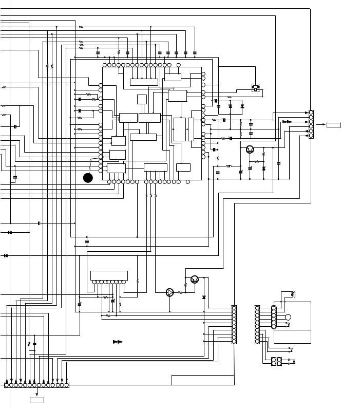
|
|
|
|
|
|
|
|
|
|
|
|
|
|
|
|
|
|
|
|
|
|
|
|
|
|
|
|
|
|
|
|
|
|
|
|
|
|
|
|
|
|
|
|
|
|
|
|
|
|
|
|
|
|
|
|
CD-C452/C452C |
||
|
|
|
|
|
|
|
|
|
|
|
R57 1K |
|
|
|
|
|
|
|
|
|
|
|
|
|
|
|
|
|
|
|
|
|
|
|
|
|
|
|
|
|
|
|
|
|
|
|
|
|
|
|
|
|
|
|
|
|
|
|
|
|
|
|
|
|
|
|
|
|
|
R61 1K |
|
|
|
|
|
|
|
|
|
|
|
|
|
|
|
|
|
|
|
|
|
|
|
|
|
|
|
|
|
|
|
|
|
|
|
|
|
|
|
|
|
|
|
|
|
|
|
|
|
|
|
|
|
|
|
|
|
|
R62 1K |
|
|
|
|
|
|
|
|
|
|
|
|
|
|
|
|
|
|
|
C44 |
100P |
|
C45 |
100P |
C47 |
100P |
C48 |
100P |
C49 |
100P |
|
|
|
|
|
|
|
|
|
|
|
|
|
|
|
||
|
|
|
|
|
|
|
|
|
|
|
R63 1K |
|
|
|
|
|
|
|
|
|
|
|
|
|
|
|
|
|
|
|
|
|
|
|
|
|
|
|
|
|
|
|
|
|
|
|
||||||||||||
|
|
|
|
|
|
|
|
1K |
1K |
|
|
C38 |
|
|
|
|
R60 |
C46 |
100P |
|
|
|
|
|
|
|
|
|
|
|
|
|
|
|
|
|
|
|
|
|
|
|
|
|||||||||||||||
|
|
|
|
|
|
|
|
|
|
0.01 |
|
|
|
|
1K |
|
|
|
|
|
|
|
|
|
|
|
|
|
|
|
|
|
|
|
|
|
|
|
|
|
||||||||||||||||||
C28 |
|
|
|
|
|
|
R58 |
R59 |
|
+B |
|
|
|
|
0V |
0V |
|
0V |
2.4V |
2.5V |
0V |
4V 4V 4V |
0V 0V |
0V |
2.4V |
0V |
2.4V |
|
0V |
|
|
|
|
|
|
|
|
|
|
|
|
|
|
|
|
|
|
|
|
|||||||||
|
|
|
|
|
|
|
|
|
|
|
|
|
64 |
63 |
62 |
61 |
60 |
59 |
58 |
57 |
56 |
55 |
54 |
|
53 |
52 |
51 |
50 |
|
|
49 |
|
|
|
|
|
|
|
|
|
|
|
|
|
|
|
|
|
|
|
|
|||||||
0.1 |
|
|
|
|
|
|
|
|
|
|
|
|
|
|
TEST1 |
|
/CS |
TEST5 |
|
4M |
16M |
|
TEST11 |
/RES |
/CQCK |
COIN SQOUT |
RWC |
WRQ FSX |
SBCK |
SFSY |
|
PW |
|
|
|
|
|
|
|
|
|
|
|
|
|
|
|
|
|
|
|
|
||||||
|
|
|
|
|
|
|
|
|
|
|
|
|
|
|
|
|
|
|
|
|
|
EFLG 48 2.2V |
|
|
|
|
|
|
|
|
|
|
|
|
||||||||||||||||||||||||
|
|
|
|
|
|
|
|
|
|
|
|
|
|
|
|
|
|
|
|
|
|
|
|
|
|
U-COM |
|
|
|
|
|
SUB-CODE |
|
|
|
SBSY 47 0V |
|
|
|
|
|
XL1 |
|
|
|
|
|
|
|
|||||||||
|
|
|
|
|
|
|
|
|
|
|
|
|
|
|
|
|
|
|
|
|
|
|
|
|
|
|
|
|
|
|
|
|
|
|
|
|
|
|
XVSS 46 0V |
|
|
|
|
|
|
|
|
|
|
|
|
|||||||
|
R44 |
|
|
|
|
|
|
|
|
|
|
0V |
1 DEF1 |
|
|
|
|
|
|
|
INTERFACE |
|
|
|
|
|
|
|
|
|
|
|
|
|
|
|
|
|
|
|
|
|
|
|
|
|
||||||||||||
|
33K |
|
|
|
|
|
|
|
|
|
R51 |
0V |
2 |
TA1 |
|
|
|
|
|
|
|
|
|
|
|
|
|
|
|
|
|
|
|
|
|
|
|
|
XIN 45 2.1V |
|
|
|
|
|
|
|
|
|
|
|
|
|||||||
3 |
|
|
|
|
|
|
|
|
|
|
|
|
|
|
|
|
|
|
|
|
|
|
|
|
|
|
|
|
|
|
|
|
|
|
X-TAL |
|
|
|
R93 |
|
|
|
|
|
|
|
|
|
||||||||||
|
|
|
|
|
|
|
|
|
|
|
3.3M |
|
|
0V |
|
|
|
|
|
|
|
|
|
|
|
|
|
|
|
|
|
|
|
|
|
|
|
|
XOUT |
44 |
2.2V |
|
|
|
|
|
|
|
|
|
|
|||||||
|
|
|
|
|
|
|
|
|
|
|
|
|
PDO |
|
|
|
|
|
|
|
|
|
|
|
|
|
|
|
|
|
GENERATOR |
|
|
|
|
|
|
|
|
|
|
|
||||||||||||||||
|
R42 |
|
|
|
|
|
|
|
|
|
C39 |
|
|
3 |
|
|
|
|
|
|
|
|
2KX8 |
|
|
|
|
|
|
|
|
|
|
C53 0.022 |
|
220 |
|
D82 1SS133 |
|
|
|
|
|
|
|
|||||||||||||
|
|
|
|
|
|
|
|
|
|
R50 |
0V |
|
|
|
|
|
|
|
|
|
|
|
RAM |
|
|
|
|
|
|
|
|
|
|
|
|
|
|
|
|
|
|
|
|
D81 1SS133 |
|
|
|
|
|
|
|
|||||||
|
47K |
|
|
|
|
|
|
|
|
|
|
|
|
|
|
|
|
|
|
|
|
|
|
|
|
|
|
|
|
|
|
|
|
|
|
|
|
|
|
|
|
|
|
|
|
|
|
|
||||||||||
|
|
|
|
|
|
|
|
|
|
0.047 |
680 |
4 |
VVSS |
|
|
|
|
|
|
|
|
|
|
|
|
|
|
|
|
|
|
|
|
|
|
|
XVDD 43 |
|
C83 0.022 |
|
|
|
|
|
|
|
||||||||||||
|
|
|
|
|
|
|
|
|
|
|
|
|
|
|
|
|
|
|
|
|
|
|
|
|
|
|
|
|
|
|
|
|
|
|
|
|
|
|
|
|
|
|||||||||||||||||
5 |
|
|
|
|
|
|
|
|
|
|
|
1.9V |
|
ISET |
|
|
|
|
|
|
|
|
|
|
|
|
|
|
|
|
|
|
|
|
|
|
|
|
|
|
|
4.8V |
|
|
|
|
|
|
|
|
||||||||
R39 |
|
|
|
|
|
|
|
|
|
C40 |
5 |
|
|
|
|
|
|
|
|
|
|
|
|
|
|
|
|
|
|
|
|
|
|
|
|
MUTER 42 4.8V |
|
|
|
|
|
R-CH |
1 |
|
||||||||||||||
|
1K |
|
|
|
|
|
|
|
|
|
|
|
|
|
|
|
|
|
|
|
|
|
|
|
|
|
|
|
|
|
|
|
|
|
|
|
|
|
|
|
RVDD 41 |
4.5V R72 |
|
|
|
|
|
|
|
|
A_GND |
|
||||||
|
|
|
|
|
|
|
|
|
|
0.047 |
|
|
|
|
|
|
|
|
|
VCO CLOCK |
ERROR COERECT |
|
|
|
|
|
|
|
|
|
|
|
|
|
|
CD_RCH |
|
|
2 |
|
||||||||||||||||||
|
|
|
|
|
|
|
|
|
|
|
R52 |
|
|
|
|
|
|
|
|
|
OSC CONTROL |
FLAG CONTROL |
|
|
|
|
|
|
|
|
|
|
RCHO 40 2V |
2.7K |
|
|
|
|
|
|
|
L-CH |
|
|||||||||||||||
|
|
|
|
|
|
|
|
|
|
|
|
|
|
|
|
|
|
|
|
|
|
|
|
|
|
4FS |
|
|
|
|
|
|
|
C74 220P |
|
|
|
|
3 |
|
||||||||||||||||||
|
|
|
|
|
|
|
|
|
|
|
27K 4.8V |
6 |
VVDD |
|
|
|
|
|
|
|
|
|
|
|
|
|
|
|
|
|
|
|
|
1BIT |
RVSS 39 0V |
|
|
C72 |
R74 |
|
|
|
|
D-GND |
CNS11 |
|||||||||||||
8 |
|
C23 |
|
|
|
|
|
|
|
R53 |
|
|
|
|
|
|
|
|
|
|
|
|
|
|
|
|
|
|
|
|
|
|
|
|
|
|
|
|
|
|
|
|
|
|
|
10/50 |
390 |
|
A_GND |
|
|
4 |
||||||
|
|
|
|
|
|
|
|
0V |
7 FR |
|
|
|
|
|
|
|
|
|
|
|
|
|
|
|
|
|
|
|
|
DIGITAL |
|
DAC |
|
|
|
|
|
|
|
|
|
C73 220P |
|
|
+B |
7.3V |
5 |
TO MAIN PWB |
||||||||||
0 |
|
0.0027 |
|
|
|
|
|
|
|
1.2K |
0V |
8 |
VSS |
|
|
|
|
|
|
|
|
|
|
|
|
|
|
|
|
|
|
|
|
|
|
|
|
LVSS 38 |
0V |
|
|
R71 |
|
R73 |
|
|
|
|
M_12V |
P16 2-A |
||||||||
|
|
|
|
|
|
|
|
|
|
|
|
|
|
|
|
SYNC-DETECT |
|
|
|
|
|
|
|
FILTER |
|
|
|
|
|
|
|
|
|
6 |
||||||||||||||||||||||||
|
|
|
|
|
|
|
|
|
|
|
|
2.5V |
9 EFMO SLICE LEVEL |
|
|
|
|
|
|
|
|
|
|
LCHO 37 2V |
|
|
2.7K |
|
390 |
|
CD_LCH |
|
|
+B |
|
|||||||||||||||||||||||
|
|
|
|
|
|
|
|
|
|
|
|
|
EFM DEMODULATE |
|
|
|
|
|
|
|
|
|
|
|
|
|
|
|
|
|
|
|
CNP11 |
|
||||||||||||||||||||||||
|
|
|
|
|
|
|
|
|
|
|
|
2.5V 10 EFMIN |
CONTROL |
|
|
|
|
IC2 |
|
|
|
|
|
|
|
|
|
|
|
|
LVDD 36 4.5V |
|
|
C71 |
|
Q52 |
|
|
|
|
||||||||||||||||||
|
|
|
|
|
|
|
|
|
|
|
|
0V |
11 TEST2 |
|
|
|
|
|
|
|
|
|
|
|
|
|
|
|
|
|
|
|
|
|
MUTEL 35 4.8V |
|
|
4.9V |
KTC3203 Y |
|
|
|
|
|
||||||||||||||
|
|
|
|
|
|
|
|
|
|
|
|
|
|
|
|
|
|
|
LC78623D |
|
|
|
|
|
|
|
|
|
|
|
10/50 +B |
|
|
|
|
|
||||||||||||||||||||||
|
|
|
|
|
|
|
|
|
|
|
|
0V |
|
CLV+ |
|
|
|
|
|
|
|
|
|
|
|
|
|
|
|
|
|
NC 34 0V |
|
|
|
|
|
|
6.5V |
|
|
|
|
|
||||||||||||||
|
|
|
|
|
|
|
|
|
|
|
|
12 |
|
|
CLV |
|
|
|
SERVO/SIGNAL |
|
|
|
|
|
|
|
|
C43 |
330/6.3 |
|
|
+5V |
5.5V |
R66 |
|
|
|
|
|
|||||||||||||||||||
|
|
|
|
|
|
|
|
|
|
|
|
0V 13 |
CLV– |
|
|
|
|
|
|
|
|
|
|
|
|
|
|
|
|
|
|
|
220 |
|
|
|
|
|
||||||||||||||||||||
|
|
|
|
|
|
|
|
|
|
|
|
DIGITAL SERVO |
|
|
|
|
|
|
|
|
|
TEST4 33 |
|
R55 |
|
|
|
|
|
|
||||||||||||||||||||||||||||
|
|
|
|
|
|
|
|
|
|
|
|
4.8V |
|
V/P |
|
|
|
|
|
|
|
|
|
CONTROL |
|
|
|
|
|
|
|
|
|
|
|
0V |
L61 |
|
|
|
|
|
|
|
|
|||||||||||||
|
|
|
|
|
|
|
|
|
|
|
|
0V |
14 |
HLF |
|
|
|
|
|
|
|
|
|
|
|
|
|
|
|
|
|
|
|
|
|
|
|
|
|
|
|
|
|
150 |
0.82 H |
|
|
R64 |
|
C75 |
|
|
|
|||||
|
|
|
|
|
|
|
|
|
|
|
|
|
|
15 |
|
|
|
SERVO |
|
|
|
|
|
|
EXTERNAL |
|
|
|
|
DIGITAL |
|
|
|
|
|
|
|
|
|
|
22 |
|
|
|
|
|||||||||||||
|
|
|
|
|
|
|
|
|
|
|
|
0V |
16 |
TES |
COMMAND |
|
|
|
|
|
|
OUTPUT |
|
|
|
|
|
|
OUT |
|
|
|
|
|
|
C50 |
C51 |
C52 |
100/16 |
ZD61 MTZJ5.6B |
|
0.001 |
|
|
||||||||||||||
|
|
|
C22 |
|
|
|
|
|
|
|
|
|
|
|
|
TOFF |
|
|
|
|
|
PCK FSEQ VDD |
CONT1 |
CONT2 |
CONT3 CONT4 |
CONT5 |
EMPH |
|
|
DOUT |
|
TEST3 |
|
|
|
|
|
|
|
|
|
|
||||||||||||||||
|
|
|
|
|
|
|
|
|
|
11 |
|
|
|
TGL |
|
|
|
C2F |
|
|
|
|
|
|
100/16 |
|
|
|
|
|
||||||||||||||||||||||||||||
|
|
|
|
|
|
|
|
|
|
|
|
|
|
JP+ |
JP– |
|
|
|
|
|
|
0.022 |
|
|
|
|
|
|||||||||||||||||||||||||||||||
|
|
|
220P |
|
|
|
|
|
|
|
|
|
|
|
|
|
|
|
|
|
|
|
|
|
|
|
|
|
||||||||||||||||||||||||||||||
|
|
|
|
|
|
|
|
|
|
|
|
|
|
|
|
|
|
|
|
|
|
|
|
|
|
|
|
|
|
|
|
|
|
|
|
|
|
|
|
|
|
|
|
|
|
|
|
|
|
|
|
|
|
|
|
|||
|
|
|
|
|
|
|
|
|
|
|
|
4.8V 17 |
18 |
19 |
20 |
21 |
22 |
23 |
|
24 |
25 |
26 |
27 |
28 29 |
|
30 |
31 |
|
32 |
|
|
|
|
|
|
|
|
|
|
|
|
|
|
|
|
|
||||||||||||
|
|
|
|
|
|
|
|
|
|
|
|
|
|
|
|
|
|
4.8V |
|
0V |
0V |
|
2.5V |
0V |
4.8V |
0V |
0V |
0V |
0V |
0V |
|
0V |
|
4.8V |
2.5V |
|
0V |
|
|
|
|
|
|
|
+B |
|
|
|
|
|
|
|
|
|
|
|||
|
|
|
|
|
|
|
|
|
|
|
|
|
|
|
|
|
|
|
|
|
|
|
|
|
|
|
|
|
|
|
|
|
|
|
|
|
|
|
|
|
|
|
|
|
|
|
|
|
|
|
|
|
|
|
|
|
|
|
|
|
|
|
|
|
|
|
|
|
|
|
|
|
|
|
|
|
|
|
|
|
|
|
|
|
|
R88 1K |
R89 1K |
R90 1K |
|
|
|
|
|
|
|
|
|
|
|
|
|
|
|
|
+B |
|
|
|
|
|
|
|
|
|
|||
|
|
|
|
|
|
|
|
|
|
|
|
|
|
|
|
|
|
|
|
|
|
|
|
|
|
|
|
|
|
|
|
|
|
|
|
|
|
|
|
|
|
|
|
|
|
|
|
|
|
|
|
|
|
|||||
|
|
|
|
|
C57 |
|
|
|
|
|
|
|
|
|
|
|
|
|
|
|
|
|
|
|
|
|
|
|
|
|
|
|
|
|
|
|
|
|
|
|
|
|
|
|
|
|
|
|
|
|
|
|
|
|
|
|
|
|
|
|
|
|
|
0.001 |
|
|
|
|
|
|
|
|
|
|
|
|
|
|
|
|
|
|
|
|
|
|
|
|
|
|
|
|
|
|
|
|
|
|
|
|
|
|
|
|
|
|
|
|
|
|
|
|
|
|
|
||
C35 |
|
|
|
|
|
|
|
|
|
|
|
|
|
|
|
|
|
|
|
|
|
|
|
|
|
|
|
|
|
|
|
|
|
|
|
|
|
|
|
|
|
|
|
|
|
|
|
|
|
|
|
|
|
|
|
|
|
|
1/50 |
|
|
|
|
|
|
|
|
|
|
|
|
|
|
|
|
|
|
|
|
|
|
|
|
|
|
|
|
|
|
|
|
|
|
|
|
|
|
|
|
|
|
|
|
|
|
|
|
|
|
|
|
|
|
|
|
|
|
D1 |
|
|
|
|
|
|
|
|
|
|
|
|
|
|
|
|
|
|
|
|
|
|
|
|
|
|
|
|
|
|
|
|
|
|
|
|
|
|
|
|
|
|
|
|
|
|
|
|
|
|
|
|
|
|
|
|
|
|
1SS133 |
|
|
|
|
|
|
|
|
|
C56 |
|
|
|
|
|
|
|
|
|
|
|
|
+B |
|
|
|
|
|
|
|
|
|
|
|
|
|
|
|
|
|
|
|
|
|
|
|
|
|
|
|
|
|
|
|
|
|||
|
|
|
|
|
|
|
|
|
|
|
|
|
|
|
|
|
|
|
|
|
|
|
|
|
|
|
|
|
|
|
|
|
|
|
|
|
|
|
|
|
|
|
|
|
|
|
|
|
|
|
|
|
|
|
|
|
||
|
|
|
|
|
|
|
|
|
|
|
|
0.022 |
|
|
|
|
|
|
|
|
|
|
|
|
|
|
|
|
|
|
|
|
|
|
|
|
|
|
|
|
|
|
|
|
|
|
|
|
|
|
|
|
|
|
|
|
|
|
|
|
|
|
|
|
|
|
|
|
|
|
|
|
CD_LD_M+ |
|
|
|
|
|
|
|
|
|
|
|
|
|
|
|
|
|
|
|
|
|
|
|
|
|
|
|
|
|
|
|
|
|
|
|
|
|
|
||||||
|
|
|
|
|
|
|
|
|
|
|
|
|
|
|
|
|
|
|
|
|
|
|
|
|
|
+B |
|
|
|
|
|
|
|
|
|
|
|
|
|
|
|
|
|
|
|
|
|
|
|
|
|
|
|
|
|
|
|
|
D4 |
|
|
|
|
|
|
|
|
|
|
|
|
|
|
|
IC81 |
|
|
|
|
|
M– |
|
|
|
|
|
|
|
|
|
|
|
|
|
|
|
|
|
|
|
|
|
|
|
|
|
|
|
|
|
|
||||||
RL104A |
|
|
|
|
|
|
|
|
|
|
|
|
TA7291S |
|
|
|
|
|
|
|
|
|
|
|
|
|
|
+B |
|
|
|
|
|
|
|
|
|
|
|
|
|
|
|
|
|
|
||||||||||||
|
|
|
|
|
|
|
|
|
|
|
|
|
|
|
|
|
|
|
|
|
|
|
|
|
|
|
|
|
|
|
|
|
|
|
|
|
|
|
|
|
|
|
|
|
|
|||||||||||||
|
|
|
|
|
|
|
|
|
|
|
LOADING MOTOR DRIVER |
|
LD |
|
|
|
|
|
|
|
|
|
|
|
|
Q91 |
|
|
|
|
|
|
|
|
|
|
|
|
|
|
|
|
||||||||||||||||
|
|
|
|
|
|
|
|
|
|
|
|
|
|
|
|
|
|
|
|
|
|
|
|
|
|
|
CD |
|
|
|
|
|
|
|
|
|
|
|
|
KTA1271 Y |
|
|
|
|
|
|
|
|
|
|
|
|
|
|||||
|
|
|
|
|
|
|
|
|
|
|
|
|
|
|
|
|
|
|
|
|
|
|
|
|
|
|
|
|
|
|
|
|
|
|
|
|
|
|
|
|
0V |
|
|
|
|
|
|
|
|
|
|
|
|
|
|
|||
|
|
|
|
|
|
|
|
|
|
|
|
1 |
2 3 |
4 |
5 6 |
7 8 9 |
|
|
|
|
|
|
|
|
|
Q93 |
|
|
|
|
12V |
|
|
|
|
|
|
|
|
|
|
|
|
|
|
|
||||||||||||
|
|
|
|
|
|
|
|
|
|
|
|
|
|
R81 |
|
|
|
|
|
|
|
|
|
|
|
12V |
|
|
|
|
|
|
|
|
|
|
|
SOLM2 |
|
|
||||||||||||||||||
|
|
|
|
|
|
|
|
|
|
|
|
0V |
6.4V |
1V |
0V |
6.5V |
6.5V |
6.5V |
2.9V |
0V |
|
|
|
|
|
|
|
|
KRC102 M |
R87 |
|
|
|
|
|
|
|
|
|
|
|
|
|
|||||||||||||||
|
|
|
|
|
|
|
|
|
|
|
|
|
|
|
2.7K |
|
|
|
|
|
0V |
|
|
|
12V |
|
|
|
|
|
|
|
|
|
|
|
|
|
|
SOLENOID |
|
|
||||||||||||||||
|
|
|
|
|
|
|
|
|
|
|
|
|
|
|
|
|
|
|
|
|
|
|
|
|
|
|
|
|
|
|
|
|
|
|
|
|
10K |
|
|
|
|
|
|
|
|
|
|
|
|
|
|
|
|
|
||||
|
|
|
|
|
|
|
|
|
|
|
|
|
|
|
|
|
|
|
|
|
|
|
|
|
|
|
|
|
|
|
|
|
3 |
|
|
|
2 |
R86 |
|
D91 |
|
|
|
|
|
|
|
|
|
|
|
|
|
LOCK |
|
|
||
|
|
|
|
|
|
|
|
|
|
|
|
|
|
|
|
|
|
|
|
|
|
|
|
|
|
|
|
|
|
|
|
|
|
0V 1 |
|
|
|
|
|
|
|
|
|
|
|
|
|
|
|
|
|
|
||||||
|
|
|
|
|
|
|
|
|
|
|
|
|
|
R83 |
|
|
|
|
|
|
|
|
|
|
|
|
|
|
|
|
|
2.2K |
|
|
|
|
|
|
|
|
|
|
|
|
|
|
|
|
|
|||||||||
|
|
|
|
|
|
|
|
|
|
|
|
|
|
|
|
|
|
R82 |
|
|
|
|
|
|
|
|
|
|
|
|
|
|
1SS133 |
|
|
|
|
|
|
|
|
|
|
|
|
|
|
|||||||||||
|
|
|
|
|
|
|
|
|
|
|
C82 |
|
|
3.9 |
|
47/16 |
|
|
|
|
|
|
|
|
|
|
|
|
|
|
|
|
|
|
|
|
|
|
|
|
|
|
|
BIM5 |
|
|
|
|
|
|||||||||
|
|
|
|
|
|
|
|
|
|
|
|
|
|
|
|
|
3.3K |
|
|
|
|
|
|
|
|
|
|
|
|
|
|
|
|
|
|
|
|
|
|
|
|
|
|
|
|
|
|
|
|
|
||||||||
|
|
|
|
|
|
|
|
|
|
|
|
|
|
|
C81 |
|
|
|
|
|
|
|
|
|
|
|
|
|
|
|
|
|
|
|
|
|
|
|
|
|
|
|
|
1 SOL |
|
|
|
|
|
|
||||||||
|
|
|
|
|
|
|
|
|
|
|
47/16 |
|
|
|
|
|
|
|
|
|
|
|
|
|
|
|
|
|
|
|
|
|
|
|
|
|
|
|
|
|
|
|
|
|
|
|
1 |
6 |
|
M3 T/T |
|
|
||||||
|
|
|
|
|
|
|
|
|
|
|
|
|
|
|
|
|
|
|
|
|
|
|
|
|
|
|
|
|
|
|
|
|
|
|
|
|
|
|
|
|
|
|
|
|
|
|
2 GND(M) |
|
2 |
5 |
+ |
|
|
|||||
|
|
|
|
|
|
|
|
|
|
|
|
|
|
|
|
|
|
|
|
|
|
|
|
|
|
|
|
|
|
|
|
|
|
|
|
|
|
|
|
|
|
|
|
|
|
|
|
|
|
|
UP/DOWN |
|
|
|||||
|
|
|
|
|
|
|
|
|
|
|
|
|
|
|
|
|
|
|
|
|
|
|
|
|
|
|
|
|
|
|
|
|
|
|
|
|
|
|
|
|
|
|
|
|
|
|
|
|
|
3 M+ |
|
|
3 |
4 |
|
|
||
|
|
|
|
|
|
|
|
|
|
|
|
|
|
|
|
|
|
R85 |
|
|
|
|
|
|
|
|
|
|
|
|
|
|
|
|
|
|
|
|
|
|
|
|
|
|
|
|
|
|
|
M LOADING |
|
|
||||||
|
|
|
|
|
|
|
|
|
|
|
|
|
|
|
|
|
|
|
|
|
|
|
|
|
|
|
|
|
|
|
|
|
|
|
|
|
|
|
|
|
|
|
|
|
|
4 M– |
|
|
4 |
3 |
– |
|
|
|||||
|
|
|
|
|
|
|
|
|
|
|
|
|
|
|
|
|
|
56 |
|
|
|
|
|
|
|
|
|
|
|
|
|
|
|
|
|
|
|
|
|
|
|
|
|
|
|
|
|
|
|
|
SW1 |
|
|
|||||
|
|
|
|
|
|
|
|
|
|
|
|
|
|
|
|
|
|
|
|
|
|
|
|
|
|
|
|
|
|
|
|
|
|
|
|
|
|
|
|
|
|
|
|
|
|
|
|
5 GND(D) |
|
5 |
2 |
|
|
|||||
|
|
|
|
|
|
|
|
|
|
|
|
|
|
|
|
|
|
(1/2W) |
|
|
|
|
|
|
|
|
|
|
|
|
|
|
|
|
|
|
|
|
|
|
|
|
|
|
|
|
|
|
OPEN |
|
|
|||||||
|
|
|
|
|
|
|
|
|
|
|
|
|
|
|
|
|
|
|
|
|
|
|
|
|
|
|
|
|
|
|
|
|
|
|
|
|
|
|
|
|
|
|
|
|
|
6 OPEN/CLOSE |
6 |
1 |
|
|
|
|||||||
|
|
|
|
|
|
|
|
|
|
|
|
|
|
|
|
|
|
|
|
|
|
|
|
|
|
|
|
|
|
|
|
|
|
|
|
|
|
|
|
|
|
|
|
|
|
|
|
|
|
|
CLOSE |
|
|
|||||
|
|
|
|
|
|
|
|
|
|
|
|
|
|
|
|
|
|
|
|
|
|
|
|
|
|
|
|
|
|
|
|
|
|
|
|
|
|
|
|
|
|
|
|
|
|
|
|
|
|
7 DISC NO. |
|
7 |
|
SENSOR |
|
|
||
|
|
|
|
|
|
|
|
|
|
|
|
|
|
|
|
|
|
|
|
|
|
|
|
|
|
|
|
|
|
|
|
|
|
|
|
|
|
|
|
|
|
|
|
|
|
|
|
|
|
8 GND(D) |
|
8 |
|
|
|
|||
|
|
|
|
|
|
|
0.022 |
|
|
|
|
|
|
|
|
|
|
|
|
|
|
|
CD SIGNAL |
|
|
|
|
|
|
|
|
|
|
|
|
|
|
|
|
|
|
9 UP/DOWN |
|
9 |
|
PWB-F |
|
|
||||||||||
|
|
|
|
|
|
C37 |
|
|
|
|
|
|
|
|
|
|
|
|
|
|
|
|
|
|
|
|
|
|
|
|
|
|
|
|
|
|
|
|
|
10 GND(D) |
10 |
|
|
|
||||||||||||||
|
|
|
|
|
|
|
|
|
|
|
|
|
|
|
|
|
|
|
|
|
|
|
|
|
|
|
|
|
|
|
|
|
|
|
|
|
CNP10 |
CNS10 |
|
|
|
|||||||||||||||||
|
|
|
R47 |
10K |
|
|
|
|
|
|
|
|
|
|
|
|
|
|
|
|
|
|
|
|
|
|
|
|
|
|
|
|
|
|
|
|
|
|
|
|
|
|
|
|
|
|
|
SW2 |
|
|
||||||||
|
|
|
|
|
|
|
|
|
|
|
|
|
|
|
|
|
|
|
|
|
|
|
|
|
|
|
|
|
|
|
|
|
|
|
|
|
|
|
|
|
|
|
|
|
|
|
|
|
|
|
||||||||
|
|
|
|
|
|
|
|
|
|
|
|
|
|
|
|
|
|
|
|
|
|
|
|
|
|
|
|
|
|
|
|
|
|
|
|
|
|
|
|
|
|
|
|
|
|
|
|
|
|
|
|
|
|
|||||
|
|
|
|
|
|
|
|
|
|
|
|
|
|
|
|
|
|
|
|
|
|
|
|
|
|
|
|
|
|
|
|
|
|
|
|
|
|
|
|
|
|
|
|
|
|
|
|
|
|
|
|
MECHA UP |
|
|||||
|
|
|
|
|
|
|
|
|
|
|
|
|
|
|
|
|
|
|
|
|
|
|
|
|
|
|
|
|
|
|
|
|
|
|
|
|
|
|
|
|
|
|
|
|
|
|
|
|
|
|
|
|
|
|
|
|
||
RWC(DSP) |
WRQ(DSP) |
CO IN(DSP) |
SQ OUT(DSP) CQ CK(DSP) |
|
DRF (ASP) |
|
|
|
|
OPEN/CLOSE DISC NO. |
UP/DOWN |
|
|
|
|
|
|
|
|
|
|
|
|
|
|
|
|
|
|
|
|
|
|
|
|
|
|
|
|
|
|
|
|
|
|
|
|
|
|
|
|
|
|
1 |
1 |
SW3 |
|
|
RES(DSP) |
|
|
|
|
|
|
|
|
|
|
|
|
|
|
|
|
|
|
|
|
|
|
|
|
|
|
|
|
|
|
|
|
|
|
|
|
|
|
|
|
|
|
|
|
|
|
2 |
2 |
|
|
||||||||
|
|
|
PUIN SW |
|
|
|
|
|
|
|
|
|
|
|
|
|
|
|
|
|
|
|
|
|
|
|
|
|
|
|
|
|
|
|
|
|
|
|
|
|
|
|
|
|
|
DISC NUMBER |
|
|||||||||||
D GND |
|
|
|
|
|
|
|
|
|
|
|
|
|
|
|
|
|
|
|
|
|
|
|
|
|
|
|
|
|
|
|
|
|
|
|
|
|
|
|
|
|
|
|
|
|
|
|
|||||||||||
SLD+ |
SLD– |
|
|
|
|
|
|
|
|
|
|
|
|
|
|
|
|
|
|
|
|
|
|
|
|
|
|
|
|
|
|
|
|
|
|
|
|
|
|
|
|
|
CNS5 |
|
|
|
|
|||||||||||
|
|
|
|
|
|
|
|
|
|
|
|
|
|
|
|
|
|
|
|
|
|
|
|
|
CD SERVO PWB-C |
|
|
|
|
|
|
|
|
|||||||||||||||||||||||||
12 |
1 2 |
3 |
4 5 |
6 |
7 |
8 9 |
10 11 |
12 13 |
14 |
|
|
|
|
|
|
|
|
|
|
|
|
|
|
|
|
|
|
|
|
|
|
|
|
|
|
|
|
|
|
|
|
|
||||||||||||||||
|
|
|
|
|
CNS12 |
|
|
|
|
|
|
|
|
|
|
|
|
|
|
|
|
|
|
|
|
|
|
|
|
|
|
|
|
|
|
|
|
|
|
|
|
|
|
|
|
|
|
|
|
|
|
|
|
|
|
|
||
|
|
|
TO DISPLAY PWB |
|
|
|
|
|
|
|
|
|
|
|
|
|
|
|
|
|
|
|
|
|
|
|
|
|
|
|
|
|
|
|
|
|
|
|
|
|
|
|
|
|
|
|
|
|
|
|
|
|
||||||
|
|
|
|
|
P19 11-A |
|
|
|
|
|
|
|
|
|
|
|
|
|
|
|
|
|
|
|
|
|
|
|
|
|
|
|
|
|
|
|
|
|
|
|
|
|
|
|
|
|
|
|
|
|
|
|
|
|
|
|
||
7 |
8 |
9 |
10 |
11 |
12 |
Figure 15 SCHEMATIC DIAGRAM (2/10)
– 15 –
 Loading...