


CD-C622/C2900
SERVICE MANUAL
No. S3908CDC622//
CD-C622
CD-C622 mini component system consisting of CD-C622 mini component system, CP-C622 and rear (GBOXS0021AWM1) speaker system.
CD-C2900
Illustration: CD-C622 |
CD-C2900 mini component system consisting of CD-C2900 mini |
component system and CP-C2900 speaker system. |
• In the interests of user-safety the set should be restored to its original condition and only parts identical to those specified be used.
Illustration: CD-C2900
CONTENTS |
|
|
Page |
IMPORTANT SERVICE NOTES (For U.S.A. Only) ........................................................................................................... |
2 |
SPECIFICATIONS .............................................................................................................................................................. |
3 |
NAMES OF PARTS ........................................................................................................................................................... |
4 |
OPERATION MANUAL ...................................................................................................................................................... |
6 |
QUICK GUIDE ................................................................................................................................................................... |
7 |
DISASSEMBLY .................................................................................................................................................................. |
9 |
REMOVING AND REINSTALLING THE MAIN PARTS ................................................................................................... |
12 |
ADJUSTMENT ................................................................................................................................................................. |
13 |
NOTES ON SCHEMATIC DIAGRAM .............................................................................................................................. |
15 |
WAVEFORMS OF CD CIRCUIT ...................................................................................................................................... |
16 |
BLOCK DIAGRAM ........................................................................................................................................................... |
17 |
SCHEMATIC DIAGRAM / WIRING SIDE OF P.W.BOARD .............................................................................................. |
20 |
VOLTAGE ........................................................................................................................................................................ |
41 |
TROUBLESHOOTING (CD SECTION) ........................................................................................................................... |
42 |
FUNCTION TABLE OF IC................................................................................................................................................ |
47 |
FL DISPLAY ...................................................................................................................................................................... |
54 |
REPLACEMENT PARTS LIST/EXPLODED VIEW |
|
PACKING OF THE SET (For U.S.A. Only) |
|
This document has been published to be used
SHARP CORPORATION– 1 – |
for after sales service only. |
|
|
|
The contents are subject to change without notice. |
CD-C622/C2900
FOR A COMPLETE DESCRIPTION OF THE OPERATION OF THIS UNIT, PLEASE REFER TO THE OPERATION MANUAL.
IMPORTANT SERVICE NOTES (For U.S.A. Only)
BEFORE RETURNING THE AUDIO PRODUCT
(Fire & Shock Hazard)
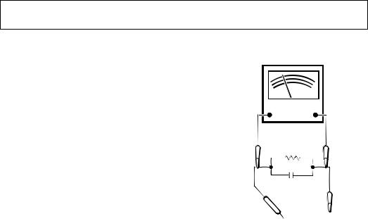
Before returning the audio product to the user, perform the following safety checks.
1.Inspect all lead dress to make certain that leads are not pinched or that hardware is not lodged between the chassis and other metal parts in the audio product.
2.Inspect all protective devices such as insulating materials, cabinet, terminal board, adjustment and compartment covers or shields, mechanical insulators etc.
3.To be sure that no shock hazard exists, check for leakage current in the following manner.
*Plug the AC line cord directly into a 120 volt AC outlet.
*Using two clip leads, connect a 1.5k ohm, 10 watt resistor paralleled by a 0.15μF capacitor in series with all exposed metal cabinet parts and a known earth ground, such as conduit or electrical ground connected to earth ground.
*Use a VTVM or VOM with 1000 ohm per volt, or higher, sensitivity to measure the AC voltage drop across the resistor (See diagram).
*Connect the resistor connection to all exposed metal parts having a return path to the chassis (antenna, metal cabinet, screw heads, knobs and control shafts, escutcheon, etc.) and measure the AC voltage drop across the resistor.
VTVM
 AC SCALE
1.5k ohms
10W
0.15 µ F |
|
|
TEST PROBE |
CONNECT TO |
|
TO EXPOSED |
KNOWN EARTH |
|
METAL PARTS |
||
GROUND |
||
|
All check must be repeated with the AC line cord plug connection reversed.
Any reading of 0.3 volt RMS (this corresponds to 0.2 milliamp. AC.) or more is excessive and indicates a potential shock hazard which must be corrected before returning the audio product to the owner.
– 2 –
CD-C622/C2900
SPECIFICATIONS
CD-C622/C2900 |
|
|
General |
|
|
Power source: |
AC 120 V, 60 Hz |
|
Power consumption: |
Stand-by; 0.3 W |
|
(CD-C622) |
Power on; 95 W |
|
Power consumption: |
Stand-by; 0.3 W |
|
(CD-C2900) |
Power on; 100 W |
|
Dimensions: |
Width; 10-5/8" (270 mm) |
|
|
|
Height; 11-13/16" (300 mm) |
|
|
Depth; 13-13/16" (351 mm) |
Weight: |
13.7 lbs. (6.2 kg) |
|
Amplifier section |
|
|
Output power: |
40 watts minimum RMS per |
|
(CD-C622 Except for |
channel into 4 ohms from 60 Hz |
|
Canada) |
to 20 kHz, 10 % total harmonic |
|
|
|
distortion |
Output power: |
Front speakers; |
|
(CD-C622 For Canada) |
MPO; 108 W (54 W + 54 W) |
|
|
|
(10 % T.H.D.) |
|
|
RMS; 60 W (30 W + 30 W) |
|
|
(10 % T.H.D.) |
|
|
Rear speakers; |
|
|
MPO; 36 W (18 W + 18 W) |
|
|
(10 % T.H.D.) |
|
|
RMS; 20 W (10 W + 10 W) |
|
|
(10 % T.H.D.) |
Output power: |
50 watts minimum RMS per |
|
(CD-C2900 Except for |
channel into 6 ohms from 60 Hz |
|
Canada) |
to 20 kHz, 10 % total harmonic |
|
|
|
distortion |
Output power: |
MPO; 180 W (90 W + 90 W) |
|
(CD-C2900 For Canada) |
(10 % T.H.D.) |
|
|
|
RMS; 100 W (50 W + 50 W) |
|
|
(10 % T.H.D.) |
Output terminals: |
Front speakers; 6 ohms |
|
(CD-C622) |
Rear Speakers; 16 ohms |
|
|
|
Headphones; 16-50 ohms |
|
|
(recommended; 32 ohms) |
Output terminals: |
Speakers; 6 ohms |
|
(CD-C2900) |
Headphones; 16-50 ohms |
|
|
|
(recommended; 32 ohms) |
Input terminal: |
Video/Auxiliary (audio signal); |
|
|
|
500 mV/47 kohms |
Tuner section |
|
|
Frequency range: |
FM; 87.5 - 108 MHz |
|
|
|
AM; 530 - 1,720 kHz |
Cassette deck section |
|
|
Frequency response: |
50 - 14,000 Hz (Normal tape) |
|
Signal/noise ratio: |
55 dB (TAPE 1, playback) |
|
|
|
50 dB (TAPE 2, recording/ |
|
|
playback) |
Wow and flutter: |
0.15 % (WRMS) |
|
Compact disc player section
Type: |
3-disc multi-play compact disc |
|
player |
Signal readout: |
Non-contact, 3-beam semi- |
|
conductor laser pickup |
D/A Converter: |
1-bit D/A converter |
Frequency response: |
20 - 20,000 Hz |
Dynamic range: |
90 dB (1 kHz) |
Front speaker section |
|
|
|
CP-C622 |
|
Type: |
2-way type [5-1/4" (13 cm) |
|
woofer and super tweeter] |
Maximum input power: |
60 W |
Rated input power: |
30 W |
Impedance: |
6 ohms |
Dimensions: |
Width; 8-11/16" (220 mm) |
|
Height; 11-13/16" (300 mm) |
|
Depth; 8-9/16" (217 mm) |
Weight: |
5.7 lbs. (2.6 kg)/each |
|
|
CP-C2900 |
|
Type: |
3-way type [5" (13 cm) woofer, |
|
2" (5 cm) tweeter and super |
|
tweeter] |
Maximum input power: |
100 W |
Rated input power: |
50 W |
Impedance: |
6 ohms |
Dimensions: |
Width; 7-7/8" (200 mm) |
|
Height; 11-13/16" (300 mm) |
|
Depth; 10" (256 mm) |
Weight: |
6.4 lbs. (2.9 kg)/each |
 Rear speaker section (CD-C622 Only)
GBOXS0021AWM1
Type: |
4" (10 cm) full range speaker |
Maximum input power: |
20 W |
Rated input power: |
10 W |
Impedance: |
16 ohms |
Dimensions: |
Width; 6-3/4" (170 mm) |
|
Height; 6-3/4" (170 mm) |
|
Depth; 3-1/2" (88 mm) |
Weight: |
0.9 lbs. (0.4 kg)/each |
Specifications for this model are subject to change without prior notice.
– 3 –

CD-C622/C2900
NAMES OF PARTS
CD-C622/C2900

 Front Panel
1.Disc Number Selector Buttons
2.Disc Tray
3.Multi-function Indicator
4.Disc Skip Button
5.Open/Close Button
6.Extra Bass Indicator
7.FM Stereo Mode Indicator
8.FM Stereo Indicator
9.(CD) Repeat Indicator
10.(CD) Play Indicator
11.(CD) Pause Indicator
12.Spectrum Analyzer/ Volume Level Indicator
13.(TAPE 2) Racord INdicator
14.(CD) Disc Number Indicators
15.(CD/TUNER) Memory Indicator
16.Timer Indicator
17.Sleep Indicator
18.(TAPE 2) Record Pause Button
19.(CD) Track Down/Review Button (TUNER) Preset Down Button (TAPE 2) Rewind Button
20.(CD) Track Up/Cue Button (TUNER) Preset Up Button (TAPE 2) Fast Forward Button
21.Timer/Sleep Button
22.Clock Button
23.Timer Set Indicator
24.Power Button
25.Equalizer Mode Selector Button
26.Dimmer Button
27.Extra Bass/Demo Mode Button
28.Headphones Socket
29.Function Selector Buttons
30.Memory/Set Button
31.(CD/TAPE) Stop Button
32.(TAPE) Play Button (CD) Play/Repeat Button
33.Tuning and Time Up/Cue Buttons
34.Volume Up/Down Buttons
35.(TAPE 1) Cassette Compartment
36.(TAPE 2) Cassette Compartment
Rear Panel
1.CD Digital Output Socket
2.AC Power Input Socket
3.FM/AM Loop Aerial Socket
4.Video/Auxiliary (Audio Signal) Input Sockets
5.Front Speaker Terminals (CD-C622 Only)
6.Rear Speaker Terminals (CD-C622)
6. Speaker Terminals (CD-C2900)
1 |
2 |
3 |
4 5 |
6 
 9
9
7

 10
10
8
 11
11
12 13 14
15
16
17
18 |
19 |
20 |
21 |
|
25 |
22 |
|
26 |
23 |
|
27 |
24 |
|
|
28 29 30 31 32 33 34
35 36
1 |
3 |
|
4 |
|
5 |
2 |
6 |
(Illistration: CD-C622)
– 4 –


 Front Speaker
CP-C622
1.Super Tweeter
2.Woofer
3.Bass Reflex Ducts
4.Speaker Wire
CP-C2900
1.Super Tweeter
2.Tweeter
3.Woofer
4.Bass Reflex Ducts
5.Speaker Wire
 Rear Speaker (CD-C622 Only)
GBOXS0021AWM1
1.Full Range Speaker
2.Speaker Wire
CD-C622/C2900

 Remote Control
1. Remote Control Transmitter LED
 CD Control section
2.Disc Number Select Buttons
3.Memory Button
4.Pause Button
5.Clear Button
6.Track Down/Review Button
7.Track Up/Cue Button
8.Disc Skip Button
9.Play/Repeat Button
10.Stop Button
11.Random Button
 Tuner control section
12. Preset Up/Down Buttons: 

 Tape control section
13.(TAPE 1) Play Button
14.(TAPE 2) Record Pause Button
15.(TAPE 1/2) Stop Button
16.(TAPE 2) Play Button
17.(TAPE 2) Rewind Button
18.(TAPE 2) Fast Forward Button
 Common section
19.Equalizer Mode Selector Button
20.Function Selector Buttons
21.Power Button
22.Extra Bass Button
23.Volume Up/Down Buttons
CD-C622/C2900
1
2

 4 3
4 3
1
2
3
4
5
1
2
1
2 |
|
|
8 |
3 |
|
|
9 |
4 |
|
|
10 |
5 |
|
|
11 |
6 |
|
|
12 |
7 |
|
|
|
|
|
|
|
13 14 |
15 |
16 |
17 18 |
19
20
21 |
23 |
22
– 5 –
– 6 –
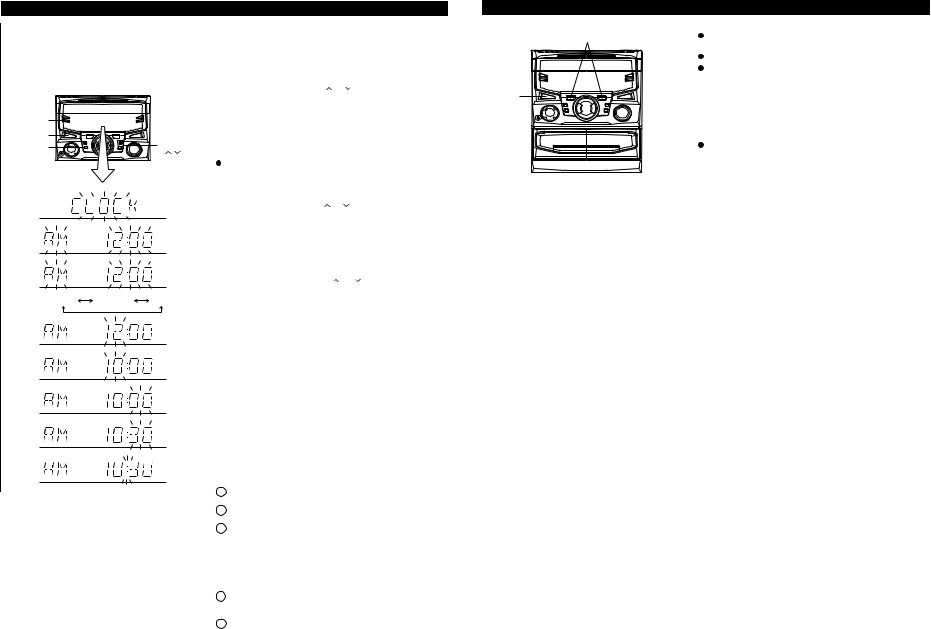
SETTING THE CLOCK
(Main unit operation)
In this example, the clock is set for the 12-hour (AM 12:00) system.
CLOCK |
|
|
POWER |
TUNING/ |
|
MEMORY/ |
TIME |
|
( ) |
||
SET |
||
|
2
3
4
AM 12:00 AM 0:00 0:00
5
6
7
8
9
1 |
Press the POWER button to enter the stand-by mode. |
2 |
Press the CLOCK button. |
3 |
Within 5 seconds, press the MEMORY/SET button. |
4 |
Press the TUNING/TIME ( or ) button to select the time |
|
display mode. |
"AM 12:00" |
→ The 12-hour display will appear. |
|
(AM 12:00 - PM 11:59) |
"AM 0:00" |
→ The 12-hour display will appear. |
|
(AM 0:00 - PM 11:59) |
"0:00" |
→ The 24-hour display will appear. |
|
(0:00 - 23:59) |
|
Note that this can only be set when the unit is first installed |
5 |
or it has been reset. |
Press the MEMORY/SET button. |
|
6 |
Press the TUNING/TIME ( or ) button to adjust the hour. |
 Press the TUNING/TIME (
  or
or  ) button once to advance the time by 1 hour. Hold it down to advance continuously.
 When the 12-hour display is selected, "AM" will change automatically to "PM".
7 |
Press the MEMORY/SET button. |
8 |
Press the TUNING/TIME ( or ) button to adjust the |
|
minutes. |
 Press the TUNING/TIME (
 or
or  ) button once to advance the time by 1 minute. Hold it down to change the time in 5 minute intervals.
 The hour setting will not advance even if minutes advance from "59" to "00".
9 Press the MEMORY/SET button.
 The clock starts operating from "0" seconds. (Seconds are not displayed.)
Note:
 In the event of a power failure or when the AC power lead is disconnected, the clock display will go out.
When the AC power supply is restored, the clock display will flash on and off to indicate the time when the power failure occurred or when the AC power lead was disconnected.
If this happens, follow the procedure below to change the clock time.
To change the clock time:
1Press the CLOCK button.
2Within 5 seconds, press the MEMORY/SET button.
3Perform steps 6 - 9 above.
To see the time display:
Press the CLOCK button.
 The time display will appear for about 5 seconds.
To change the time display mode:
1Perform steps 1 - 2 in the section "RESETTING THE MICROCOMPUTER", on page 19.
2Perform steps 1 - 9 above.
RESETTING THE MICROCOMPUTER
2
1,2
Reset the microcomputer under the following conditions:
To erase all of the stored memory contents (clock and timer settings, and tuner and CD presets).
If the display is not correct.
If the operation is not correct.
1 Press the POWER button to enter the stand-by mode.
2 Whilst pressing down the 


 button and the


 button, hold down the POWER button for at least 1 second.
Caution:
The operation explained above will erase all data stored in memory including clock and timer settings, and tuner and CD presets.
C622/C2900-CD
MANUAL OPERATION

MINI COMPONENT SYSTEM
Quick Guide/Guía rápida CD-C622
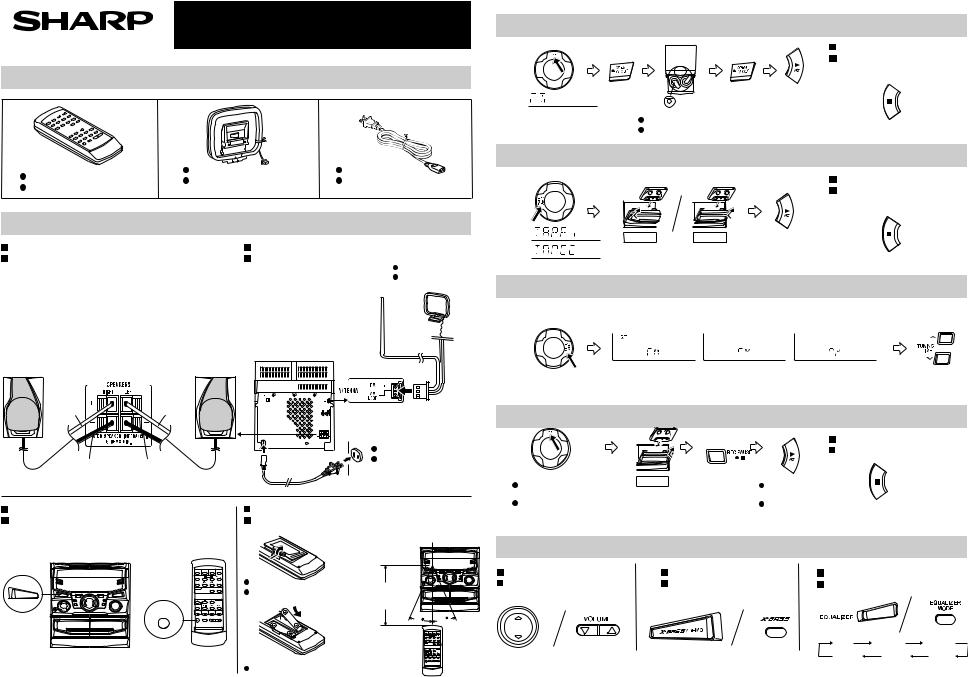
1 Check the supplied accessories / Compruebe los accesorios suministrados
Remote control x 1 |
FM/AM loop antenna x 1 |
AC power cord x 1 |
Antena de cuadro de |
Cable de alimentación |
|
Controlador remoto x 1 |
FM/AM x 1 |
de CA x 1 |
2 Preparation for use / Preparación para su uso
Speaker connection |
|
|
Antenna connection |
|
|
|
Conexión de los altavoces |
|
Conexión de las antenas |
AM Loop Antenna |
|||
Rear speaker (Right) |
|
Rear speaker (Left) |
|
|
Antena de cuadro |
|
Altavoz trasero (Derecho) |
|
Altavoz trasero (Izquierdo) |
|
|
de AM |
|
|
|
|
|
FM Antenna |
|
|
– |
Black |
|
|
Antena de FM |
|
|
Negro |
|
|
|
|
|
|
– 7 |
|
Wire with the |
|
|
|
|
Wire with the |
|
|
|
|
|
|
|
white line |
|
|
|
|
|
white line |
|
|
|
|
|
|
|
Cable con la |
|
|
|
|
|
Cable con la |
|
|
|
|
|
|
|
línea blanca |
|
|
|
|
|
línea blanca |
|
|
|
|
|
|
|
|
|
|
|
|
|
Red |
|
Red |
|
|
|
|
Rojo |
|
Rojo |
|
|
|
|
|
Black |
|
|
|
AC 120 V, 60 Hz |
|
|
|
|
|
120 V de CA, 60 Hz |
||
Front speaker (Right) |
Negro |
Front speaker (Left) |
|
|
|
|
Altavoz delantero |
|
Altavoz delantero |
|
|
|
|
(Derecho) |
|
(Izquierdo) |
|
|
|
|
Turning the power on and off |
|
Remote control |
|
|
||
Conexión y desconexión de la alimentación |
Controlador remoto |
Remote Sensor |
||||
|
|
|
|
|
||
|
|
|
|
|
Sensor remoto |
|
|
|
|
2 “AA” batteries |
8” - 20’ (0.2m - 6m) |
|
|
POWER |
|
|
Dos pilas “AA” |
|
||
|
|
0,2m - 6m |
|
|
||
|
|
|
|
|
|
|
|
|
POWER |
|
|
|
15 |
|
|
|
|
|
15 |
|
 Batteries are not included.
 Las pilas no están incluidas.
3 Listening to a CD / Audición de discos CD
 To stop the playback
 Para detener la reproducción
 Label facing up
 Etiqueta hacia arriba
4 Listening to a tape / Audición de una cinta
 To stop the playback
 Para detener la reproducción
TAPE 1 |
TAPE 2 |
|
|
5 Listening to the radio / Audición de la radio
6 Recording from CDs / Grabaciones de discos CD
|
|
To stop the playback |
|
|||
|
|
Para detener la reproducción |
|
|||
Load the disc to be |
TAPE 2 |
CD recording |
|
|
|
|
recorded. |
|
starts. |
|
|
|
|
Introduzca el disco |
|
La grabación de |
|
|
|
|
que va a grabar. |
|
CD empieza. |
|
|
|
|
7 Sound control / Control del sonldo |
|
|
|
|
||
Volume |
Extra bass (X-BASS) |
Pre-programmed equalizer |
-CD |
|||
Volumen |
Graves extra (X-BASS) |
Ecualizador preprogramado |
||||
C622/C2900 |
||||||
VOLUME |
|
|
|
|
||
|
|
FLAT |
HEAVY-1 |
HEAVY-2 |
|
|
|
|
SOFT-2 |
SOFT-1 |
VOCAL |
|
|
MINI COMPONENT SYSTEM
Quick Guide/Guía rápida CD-C2900
1 Check the supplied accessories / Compruebe los accesorios suministrados
|
Remote control x 1 |
FM/AM loop antenna x 1 |
AC power |
|
||
|
Antena de cuadro de |
Cable de alimentación |
||||
|
Controlador remoto x 1 |
|||||
|
FM/AM x 1 |
|
de CA x 1 |
|
||
|
|
|
|
|||
|
2 Preparation for use / Preparación para su uso |
|
|
|||
|
Speaker connection |
|
Antenna connection |
|
|
|
|
Conexión de los altavoces |
|
Conexión de las antenas |
AM Loop Antenna |
||
|
|
|
|
|
||
|
|
|
|
|
Antena de cuadro |
|
|
|
|
|
|
de AM |
|
|
|
|
|
FM Antenna |
|
|
|
|
|
|
Antena de FM |
|
|
8 – |
Front speaker |
Front speaker |
|
|
|
|
– |
(Right) |
(Left) |
|
|
|
|
|
Altavoz delantero |
Altavoz delantero |
|
|
|
|
|
(Derecho) |
(Izquierdo) |
|
|
|
|
|
Red |
Red |
|
|
|
|
|
Rojo |
Rojo |
|
|
|
|
|
|
|
|
|
AC 120 V, 60 Hz |
|
|
Black |
Black |
|
|
120 V de CA, 60 Hz |
|
|
|
|
|
|
||
|
Negro |
Negro |
|
|
|
|
|
Turning the power on and off |
Remote control |
|
|
|
|
|
Conexión y desconexión de la alimentación |
Controlador remoto |
Remote Sensor |
|||
|
|
|
|
|
||
|
|
|
|
|
Sensor remoto |
|
|
|
|
2 “AA” batteries |
8” - 20’ (0.2m - 6m) |
|
|
|
POWER |
|
Dos pilas “AA” |
|
||
|
|
0,2m - 6m |
|
|
||
|
|
|
|
|
|
|
|
|
POWER |
|
|
|
15 |
|
|
|
|
|
15 |
|
 Batteries are not included.
Las pilas no están incluidas.
3 Listening to a CD / Audición de discos CD |
|
-CD |
|
|
|
To stop the playback |
C622/C2900 |
|
|
|
|
|
|
Para detener la reproducción |
|
Label facing up |
|
|
|
Etiqueta hacia arriba |
|
|
|
4 Listening to a tape / Audición de una cinta |
|
|
|
|
|
To stop the playback |
|
|
|
Para detener la reproducción |
|
TAPE 1 |
TAPE 2 |
|
|
5 Listening to the radio / Audición de la radio
6 Recording from CDs / Grabaciones de discos CD
|
|
To stop the playback |
|
|
Para detener la reproducción |
Load the disc to be |
TAPE 2 |
CD recording |
|
||
recorded. |
|
starts. |
Introduzca el disco |
|
La grabación de |
que va a grabar. |
|
CD empieza. |
7 Sound control / Control del sonldo
Volume |
Extra bass (X-BASS) |
Pre-programmed equalizer |
||
Volumen |
Graves extra (X-BASS) |
Ecualizador preprogramado |
||
VOLUME |
|
|
|
|
|
|
FLAT |
HEAVY-1 |
HEAVY-2 |
|
|
SOFT-2 |
SOFT-1 |
VOCAL |
CD-C622/C2900
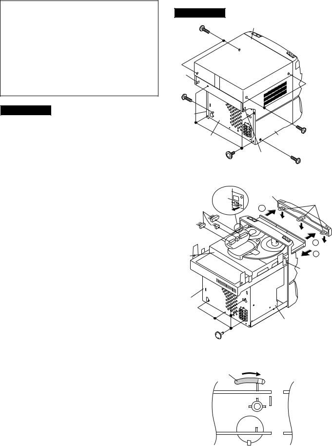
DISASSEMBLY
Caution on Disassembly
Follow the below-mentioned notes when disassembling the unit and reassembling it, to keep it safe and ensure excellent performance:
1.Take cassette tape and compact disc out of the unit.
2.Be sure to remove the power supply plug from the wall outlet before starting to disassemble the unit.
3.Take off nylon bands or wire holders where they need be removed when disassembling the unit. After servicing the unit, be sure to rearrange the leads where they were before disassembling.
4.Take suffcient care on static electricity of integrated circuits and other circuits when servicing.
CD-C622/C2900
STEP |
REMOVAL |
|
PROCEDURE |
|
FIGURE |
|
|
|
|
|
|
1 |
Top Cabinet |
1. |
Screw ..................... |
(A1) x4 |
9-1 |
|
|
|
|
|
|
2 |
Side Panel |
1. |
Screw ..................... |
(B1) x6 |
9-1 |
|
(Left/right) |
2. Hook ....................... |
(B2) x2 |
|
|
|
|
|
|
|
|
3 |
CD Player Unit/ |
1. |
Turn on the power supply, |
9-2 |
|
|
CD Tray Cover |
|
open the disc tray, take out |
|
|
|
|
|
the CD cover, and close. |
|
|
|
|
|
(Note 1) |
|
|
|
|
2. |
Hook ....................... |
(C1) x3 |
|
|
|
3. |
Hook ....................... |
(C2) x2 |
|
|
|
4. |
Socket .................... |
(C3) x3 |
|
|
|
|
|
|
|
4 |
Back Board |
1. Screw ..................... |
(D1) x5 |
9-2 |
|
|
(with Digital |
|
|
|
|
|
Output PWB) |
|
|
|
|
|
|
|
|
|
|
5 |
Main PWB |
1. Screw ..................... |
(E1) x3 |
10-1 |
|
|
|
2. |
Socket .................... |
(E2) x4 |
|
|
|
3. |
Flat Wire ................. |
(E3) x1 |
|
|
|
4. |
Tip Wire .................. |
(E4) x1 |
|
|
|
5. |
Flat Cable .............. |
(E5) x1 |
|
|
|
|
|
|
|
6 |
Front Panel |
1. |
Screw ..................... |
(F1) x1 |
10-1 |
|
|
|
|
|
|
7 |
Display PWB/ |
1. |
Socket .................... |
(G1) x1 |
10-2 |
|
Switch PWB |
2. |
Screw ..................... |
(G2) x12 |
|
|
|
|
|
|
|
8 |
Tape Mechanism |
1. |
Open the cassette holder. |
10-2 |
|
|
|
2. |
Screw...................... |
(H1) x5 |
|
|
|
|
|
|
|
9 |
Headphones PWB |
1. |
Screw ..................... |
(J1) x1 |
10-2 |
|
|
2. |
Support Bracket ..... |
(J2) x1 |
|
|
|
|
|
|
|
10 |
Turntable |
1. Screw ..................... |
(K1) x1 |
10-3 |
|
|
|
2. |
Cover ..................... |
(K2) x1 |
|
|
|
|
|
|
|
11 |
Disc Tray |
1. Screw ..................... |
(L1) x2 |
10-3 |
|
|
|
2. |
Guide ..................... |
(L2) x2 |
|
|
|
|
|
|
|
12 |
CD Servo PWB |
1. |
Screw ..................... |
(M1) x1 |
10-4 |
|
(Note 2) |
2. |
Socket .................... |
(M2) x4 |
|
|
|
|
|
|
|
13 |
CD Changer |
1. Screw ..................... |
(N1) x4 |
10-5 |
|
|
Mechanism |
|
|
|
|
|
|
|
|
|
|
14 |
CD Mechanism |
1. |
Screw ..................... |
(P1) x1 |
10-5 |
|
|
|
|
|
|
Note 1:
How to open the changer manually. (Fig. 9-3)
1. Change, turn fully the lock lever in the arrow direction through the hole on the loading chassis bottom in this state. After that, push forward the CD player base.
Note 2:
1.After removing the connector for the optical pickup fromthe connector wrap the conductive aluminium foil around the front end of connector so as to protect the optical pickup from electrostatic damage.
(Illustration: CD-C622)
CD-C622/C2900
Top Cabinet
(A1)x2
ø3x12mm
(B2)x1
(B1)x1
ø3x8mm
Side Panel |
|
|
(Right) |
|
|
|
|
(A1)x2 |
|
|
ø3x12mm |
Back Board |
Side Panel |
|
|
(Left) |
|
(B1)x4 |
(B2)x1 |
|
ø3x8mm |
(B1)x1 |
|
|
ø3x8mm |
|
|
Figure 9-1 |
|
(C2) x1 |
CD Tray Cover |
Hook |
|
||
Pull |
|
( C1) x3 |
1 |
|
|
(C3) x3 |
|
|
|
|
1 |
CD Player |
|
2 |
Unit |
|
|
|
|
( C2 ) x1 |
Back Board
Main PWB

 (D1)x5 ø3x8mm
Figure 9-2
LOCK
LEVER
Figure 9-3
– 9 –
CD-C622/C2900
(E1)x1
ø3x10mm
(E2)x2 |
Front Panel |
|
(E3)x1
(E5)x1
(E2)x2
(E4)x1
(G1)x1
(E1)x2 
 ø3x8mm
Main PWB |
(F1)x1 |
|
ø3x8mm |
Figure 10-1
(G1)x1
Switch PWB
Front Panel
(G2)x2 
 ø3x10mm
Display PWB
(G2)x10
ø3x10mm  Headphones PWB
 Open
Open
(J2)x1
Cassette
Holder
(J1)x1 |
Tape Mechanism |
|
ø3x10mm |
||
(H1)x5 |
||
|
||
|
ø3x10mm |
Figure 10-2
( K1 ) x1 ø3 x10mm 
( K2 ) x1
Washer
Turntable
Disc Tray
( L1 ) x1 ø3 x10mm
( L2 ) x1
( L1 ) x1 ø3 x10mm
CD Player Unit |
( L2 ) x1 |
|
|
Figure 10-3 |
|
( M1 ) x1 ø3 x10mm
CD Servo PWB
( M2 ) x2
( M2 ) x2
CD Player Unit
Figure 10-4
 ( N1 ) x4
ø3 x12mm
( P1 ) x1 ø2.6 x10mm
Shift Lever
CD Changer
Mechanism
CD Player Base |
CD Mechanism |
Care when installing the CD changer mechanism.
Install the CD changer mechanism on the CD player base after the shift lever has been set in the highest position.
Figure 10-5
– 10 –
CP-C622
STEP |
REMOVAL |
|
PROCEDURE |
|
FIGURE |
|
|
|
|
|
|
1 |
Front Speaker |
1. Front Panel ............ |
(A1) x1 |
11-1 |
|
|
|
2. |
Tip .......................... |
(A2) x2 |
|
|
|
3. |
Screw ..................... |
(A3) x4 |
|
|
|
|
|
|
|
Note:
The rear speakers can be easily disassembled. Therefore the disassembling method is not discribed.
For details refer to the disassembling drawing in the Parts Guide.
CD-C622/C2900
CP-C622 |
|
|
|
Front Panel |
Piezo |
(A3)x4 |
(A2)x2 |
(A1)x1 |
|
ø4x12mm |
|
|
|
|
Woofer
Screw Driver
|
|
|
|
|
|
|
Figure 11-1 |
|
CP-C2900 |
|
|
|
|
CP-C2900 |
|
STEP |
REMOVAL |
PROCEDURE |
|
FIGURE |
|
|
|
1 |
Front Speaker 1. Front Panel ............ |
(A1) x1 |
11-2 |
Front Panel |
Super |
Tweeter |
|
|
2. |
Tip |
(A2) x2 |
|
Tweeter |
||
|
|
(A1)x1 |
|
(A3)x2 |
|||
|
3. |
Screw |
(A3) x2 |
|
|
||
|
|
|
|
ø3x10mm |
|||
|
4. |
Screw |
(A4) x2 |
|
|
|
|
|
|
|
|
|
|||
|
5. |
Screw ..................... |
(A5) x4 |
|
|
|
(A2)x2 |
(A4)x2 
 ø3x10mm
(A5)x4
ø4x14mm
Woofer
Screw Driver
Figure 11-2
– 11 –

CD-C622/C2900
REMOVING AND REINSTALLING THE MAIN PARTS
CD MECHANISM SECTION
Perform steps 1, 2, 3, 13 and 14 of the disassembly method to remove the CD mechanism.
How to remove the loading motor (See Fig. 12-1)
1.Remove the screws (A1) x 2 pcs., to remove the loading motor.
How to remove the pickup (See Fig. 12-2)
1.Remove the screws (B1) x 2 pcs., to remove the shaft (B2).
2.Remove the stop washer (B3) x 1 pc., to remove the gear (B4).
3.Remove the pickup.
Note
After removing the connector for the optical pickup fromthe connector wrap the conductive aluminium foil around the front end of connector so as to protect the optical pickup from electrostatic damage.
Loading / Up
/ Down Motor
Motor
PWB 
( A1 ) x2  ø2.6 x5mm
Figure 12-1
( B1 ) x2 |
Stop Washer |
|
( B3 ) x1 |
||
ø2.6 x6mm |
||
|
Pickup
Shaft |
CD Mechanism |
|
Gear |
||
( B2 ) x1 |
||
( B4 ) x1 |
||
|
||
|
Figure 12-2 |
– 12 –

CD-C622/C2900
ADJUSTMENT
MECHANISM SECTION
∙ Driving Force Check
Torque Meter |
Specified Value |
|
|
Play: TW-2412 |
Tape 1: Over 80 g |
|
Tape 2: Over 80 g |
|
|
∙ Torque Check
Torque Meter |
Specified Value |
|
|
|
|
|
Tape 1 |
Tape 2 |
|
|
|
Play: TW-2111 |
30 to 60 g. cm |
30 to 60 g.cm |
|
|
|
Fast forward: TW-2231 |
— |
60 to 120 g.cm |
|
|
|
Rewind: TW-2231 |
— |
60 to 120 g.cm |
|
|
|
∙ Tape Speed |
|
|
|
Test Tape |
Adjusting |
Specified |
Instrument |
|
|
Point |
Value |
Connection |
|
|
|
|
|
Normal |
MTT-111 |
Volume in |
3,000 ± |
Speaker |
speed |
|
motor. |
30 Hz |
terminal |
|
|
(MM1) |
|
(Load |
|
|
|
|
resistance: |
|
|
|
|
8 ohms) |
|
|
|
|
|
TUNER SECTION
fL: Low-range frequency fH: High-renge frequency
∙ AM IF/RF
Signal generator: 400 Hz, 30%, AM modulated
Test Stage |
Frequency |
Frequency |
Setting/ |
Instrument |
|
|
|
|
Display |
Adjusting |
Connection |
|
|
|
|
Parts |
|
IF |
450 kHz |
|
1,720 kHz |
T351 |
*1 |
Band |
— |
|
530 kHz |
(fL): T333 |
*2 |
Coverage |
|
|
|
1.1 ± 0.1 V |
|
|
|
|
|
|
|
Tracking |
990 kHz |
|
990 kHz |
(fL): T331 |
*1 |
*1. Input: Antenna, |
Output: TP302 |
|
|
||
*2. Input: Antenna, |
Output: TP301 |
|
|
||
TAPE MECHANISM
MM 1
Motor
Volume in motor
MAIN PWB
∙ FM RF
Signal generator: 1 kHz, 75 kHz dev., FM modulated
Test Stage |
Frequency |
Frequency |
Serring/ |
Instrument |
|
|
Display |
Adjusting |
Connection |
|
|
|
Point |
|
|
|
|
|
|
Band |
— |
87.50 MHz |
L303(fL): |
*1 |
Coverage |
|
|
3.4 V ± 50 mV |
|
|
|
|
|
|
RF |
98.00 MHz |
98.00 MHz |
L302 |
*2 |
|
(10-30 dB) |
|
|
|
|
|
|
|
|
*1. Input: Antenna, |
Output: TP301 |
*2. Input: Antenna, |
Output: Speaker terminal |
∙ Detection
Signal generator: 10.7 MHz, FM sweep generator
Test |
Frequency |
Frequency |
Adjusting |
|
Instrument |
|||
Stage |
|
|
Display |
|
Parts |
|
Connection |
|
|
|
|
|
|
|
|
|
|
Detection |
10.7 MHz |
98.00 MHz |
|
T352 |
|
Input: Pin 1 of |
||
|
|
|
|
|
|
|
|
IC303 |
|
|
|
|
|
|
|
|
Output: TP302 |
|
|
|
|
|
|
|
|
|
IF |
10.7 MHz |
98.00 MHz |
|
T301(Turn |
|
Input: Pin 1 of |
||
|
|
|
|
|
|
the core of |
|
IC301 |
|
|
|
|
|
|
transformer |
|
Output: TP302 |
|
|
|
|
|
|
T352 fully |
|
|
|
|
|
|
|
|
counter- |
|
|
|
|
|
|
|
|
clookwise.) |
|
|
∙ VCO Frequency |
|
|
|
|
|
|
||
|
|
|
|
|
|
|
||
Frequency |
Frequency |
|
|
Adjusting |
|
Instrument |
||
|
|
Display |
|
|
Parts |
|
Connection |
|
98.00 MHz |
98.00 MHz |
|
VR351* |
|
Pin 13, Pin 21 |
|||
(60 dB) |
|
|
|
|
|
|
|
and ground |
|
|
|
|
|
|
|
|
of IC303 |
* Adjust for 76 kHz ± 200 Hz. |
|
|
|
|
|
|||
Notes:
After preparing the test circuit shown in Fig 13-2, connect the Pin 13 , Pin 21 and ground of the IC303 with test circuit, and measure the Value.
At this time, apply a standard unmodulated signal input and adjust the VCO.
Pin 13 of IC303 Pin 21 of IC303 |
|
||
G |
D |
FET : 2SK19 or 2SK54 |
|
|
|
||
|
|
|
|
|
S |
|
TO FREQUENCY |
|
|
|
COUNTER |
|
|
10 kΩ |
|
1 |
L301 |
Figure 13-2 |
|
|
|
|
IC301 |
|
|
|
|
|
|
L302 |
CNP301 |
|
|
L303 |
T301 |
AM LOOP |
||
FM BAND |
FM RF |
ANTENNA |
|||
|
FM IF |
||||
|
|
|
|||
COVERAGE fL |
|
|
|
||
|
|
|
|
||
|
T351 |
|
|
T331 |
|
|
AM IF |
TP301 |
|
AM TRACKING |
|
|
|
|
|
fL |
|
|
1 |
T333 |
|
AM BAND |
|
|
IC303 |
|
|
||
|
T352 |
|
COVERAGE fL |
||
13 |
21 |
|
|||
|
|
||||
|
R340 |
FM DET |
|
||
|
|
|
|
||
|
VR351 |
|
|
|
|
|
VCO |
TP302 |
|
||
Figure 13-1 ADJUSTMENT POINTS
– 13 –
CD-C622/C2900
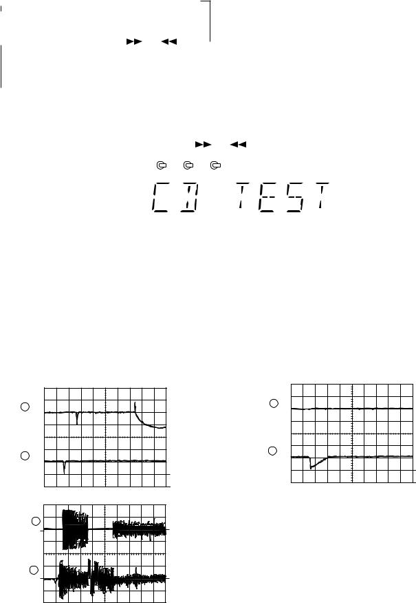
TEST MODE
• Setting the test mode
Any one of test mode can be set by pressing several keys as follows. <REC. PAUSE> + <DISC. SKIP> + <POWER> TEST: CD operation test
• TEST mode
Function — CD test mode
Setting of TEST mode
Indication of CD TST mode (Fig. 14-1)
|
OPEN/CLOSE operation is manual operation. |
) or ( |
) key. |
|
IL is not performed. |
||||||
|
|||||||||||
|
|
|
|
|
|||||||
|
|
|
|
|
|
|
|||||
The pickup can be moved by using the ( |
|
|
|||||||||
|
|
|
|||||||||
|
|
<MEMORY> |
|
<MEMORY> |
|
|
<MEMORY> |
<STOP> |
|||
|
|
LASER ON |
|
Tracking on the spot. |
|
|
Tracking on the spot. |
|
STOP |
||
|
|
|
|
SERVO OFF PLAY |
|
|
SERVO ON PLAY |
|
|
||
|
|
<PLAY> key input |
|
TOC. IL is performed, and the ordinary PLAY is performed. |
|
Press <STOP> key. |
|
Stop |
||||
|
|
|
|
|
||||||||
|
|
|
|
If the following key is pressed during PLAY, it is possible |
|
|
|
|
||||
|
|
|
|
to specify directly any Track No. |
|
|
|
|
|
|
|
|
|
|
|
|
<Disc Number 1> key: Track 4 |
|
|
|
|
|
|
|
|
|
|
|
|
<Disc Number 2> key: Track 9 |
|
|
|
|
|
|
|
|
|
|
|
|
<Disc Number 3> key: Track 15 |
|
|
|
|
|
|
|
|
Note: |
|
|
|
|
|
|
|
|
|
|
||
Only in STOP state it is possible to slide the pickup with the ( |
) or ( |
) key. |
|
|
|
|
||||||
VOL. --- Last memory |
|
|
|
|
|
|
|
|
|
|
||
BAL. --- CENTER |
|
|
1 |
2 |
3 |
|
|
|
|
|
||
R.GEQ. --- FLAT |
|
|
|
|
|
|
||||||
X-BAS --- OFF |
|
|
|
|
|
|
|
|
|
|
||
Canceling method - POWER OFF |
|
|
|
|
|
|
|
|
||||
|
|
|
|
|
|
|
|
|
|
|
|
|
Figure 14-1
CD SECTION
Since this CD system incorporates the following automatic adjustment function, when the pickup is replaced, it is not necessary to readjust it.
Since this CD unit does not need adjustment, the combination of PWB and laser pickup unit is not restricted.
• Automatic adjustment item
1.Focus offset (Fig. 14-2)
2.Tracking offset (Fig. 14-3)
3.E/F balance (tracking error balance) (Fig. 14-4)
4.RF level AGC function (HF level: constant)
5.RF level automatic follow-up of the tracking gain
This automatic adjustment is performed each time a disc is changed. Therefore, each disc is played back using the optimal settings.
0.1s |
|
|
0.50 V |
|
|
IC1 20 |
FE |
|
|
|
FOCUS |
|
|
OFF-SET |
|
|
ADJUST |
0.1s |
|
|
0.50 V |
|
|
IC1 7 |
TE |
TRACKING |
|
|
|
|
|
OFF-SET |
|
|
1 ADJUST |
|
2 |
|
|
Figure 14-2 |
|
200 ms |
TRACKING/ |
|
1V/diV |
ERROR |
|
IC 1 15 |
BARANCE |
|
TO |
1 ADJUST |
|
|
||
200 ms |
|
|
1V/diV |
|
|
IC 1 7 |
2 |
|
TE |
||
|
||
|
Figure 14-4 |
10ms 0.50 V
IC1 20 FE
10ms 0.50 V IC1 7 TE
Figure 14-3
Enlarged
View
TRACKING
OFF-SET 1 ADJUST
2
– 14 –
CD-C622/C2900
NOTES ON SCHEMATIC DIAGRAM
∙Resistor:
To differentiate the units of resistors, such symbol as K and M are used: the symbol K means 1000 ohm and the symbol M means 1000 kohm and the resistor without any symbol is ohm-type resistor. Besides, the one with “Fusible” is a fuse type.
∙Capacitor:
To indicate the unit of capacitor, a symbol P is used: this symbol P means micro-micro-farad and the unit of the capacitor without such a symbol is microfarad. As to electrolytic capacitor, the expression “capacitance/withstand voltage” is used.
(CH), (TH), (RH), (UJ): Temperature compensation (ML): Mylar type
(P.P.): Polypropylene type
∙Schematic diagram and Wiring Side of P.W.Board for this model are subject to change for improvement without prior notice.
∙The indicated voltage in each section is the one measured by Digital Multimeter between such a section and the chassis with no signal given.
1.In the tuner section, ( ) indicates AM
< > indicates FM stereo
2.In the main section, a tape is being played back.
3.In the deck section, a tape is being played back. ( ) indicates the record state.
4.In the power section, a tape is being played back.
5.In the CD section, the CD is stopped.
∙Parts marked with “ ” (
” ( 


 ) are important for maintaining the safety of the set. Be sure to replace these parts with specified ones for maintaining the safety and performance of the set.
REF. NO |
DESCRIPTION |
POSITION |
|
|
|
SW1 |
OPEN/CLOSE |
ON—OFF |
|
|
|
SW2 |
MECHA UP |
ON—OFF |
|
|
|
SW3 |
DISC NUMBER |
ON—OFF |
|
|
|
SW4 |
PICKUP IN |
ON—OFF |
|
|
|
SW701 |
POWER |
ON—OFF |
|
|
|
SW703 |
CLOCK |
ON—OFF |
|
|
|
SW704 |
TIMER/SLEEP |
ON—OFF |
|
|
|
SW705 |
DISC 1 |
ON—OFF |
|
|
|
SW706 |
DISC 2 |
ON—OFF |
|
|
|
SW707 |
DISC 3 |
ON—OFF |
|
|
|
SW708 |
DISC SKIP |
ON—OFF |
|
|
|
SW709 |
OPEN/CLOSE |
ON—OFF |
|
|
|
SW710 |
REV |
ON—OFF |
|
|
|
SW711 |
REC PAUSE |
ON—OFF |
|
|
|
SW712 |
MEMORY/SET |
ON—OFF |
|
|
|
SW713 |
STOP |
ON—OFF |
|
|
|
FRONT
VIEW
E |
C |
B |
(S) |
(G) |
(D) |
(1) |
(2) |
(3) |
KTA1266 GR |
|
KRC104 M |
2SA1015 GR |
|
KRC107 M |
2SA1318 |
|
KTA1271 Y |
2SC3331 |
|
KTA1273 Y |
2SC535 C |
|
KTA1274 Y |
KRA102 M |
|
KTD2058 Y |
KRA109 M |
|
KTC3200 GR |
KRC102 M |
|
KTC3203 Y |
REF. NO |
DESCRIPTION |
POSITION |
|
|
|
SW714 |
TUNER/BAND |
ON—OFF |
|
|
|
SW715 |
VIDEO |
ON—OFF |
|
|
|
SW716 |
TAPE |
ON—OFF |
|
|
|
SW717 |
CD |
ON—OFF |
|
|
|
SW722 |
FF |
ON—OFF |
|
|
|
SW723 |
TUNING UP |
ON—OFF |
|
|
|
SW724 |
TUNING DOWN |
ON—OFF |
|
|
|
SW725 |
PLAY |
ON—OFF |
|
|
|
SW726 |
VOLUME DOWN |
ON—OFF |
|
|
|
SW727 |
VOLUME UP |
ON—OFF |
|
|
|
SW728 |
X-BASS/DEMO |
ON—OFF |
|
|
|
SW729 |
EQUALIZER |
ON—OFF |
|
|
|
SW730 |
DIMMER |
ON—OFF |
|
|
|
SWM 3 |
FOOL PROOF |
ON—OFF |
|
|
|
SWM 4 |
F.A.S. |
ON—OFF |
|
|
|
SWM 5 |
CAM |
ON—OFF |
|
|
|
FRONT VIEW
L1154GT4
SLI342YCB
SLI342DCB
SLI342UCB
SLI342YCJ
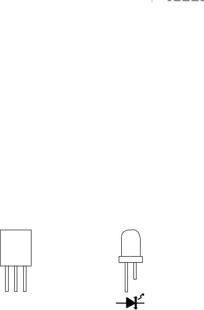
Figure 15 TYPES OF TRANSISTOR AND LED
– 15 –
CD-C622/C2900
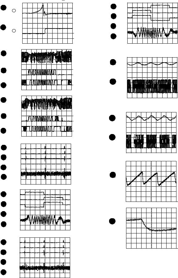
WAVEFORMS OF CD CIRCUIT
STOP  PLAY
PLAY
FOCUS SERCH
1 |
5ms |
|
|
|
0.50 V |
F.E |
|
||
|
IC1 20 |
|
||
2 |
5ms |
|
|
|
5.0 V |
|
|
||
|
IC1 54 |
DRF |
3 |
|
|
|
|
||
|
|
|
1 |
|
3 |
0.5ms |
CUE |
||
|
||||
1.00 V |
|
|||
|
HF |
|
||
4 |
0.5ms |
1 |
||
5.0 V |
2 |
|||
|
HFL |
|||
|
|
|||
5 |
0.5ms |
3 |
||
|
||||
5.0 V |
|
|||
|
TES |
|
||
3 |
0.5ms |
REVIEW |
||
1.00 V |
|
|||
|
HF |
|
||
4 |
0.5ms |
1 |
||
5.0 V |
2 |
|||
|
HFL |
|||
5 |
0.5ms |
3 |
||
5.0 V |
|
|||
|
TES |
|
||
6 |
50ms |
CUE |
||
10.0 V |
||||
|
||||
|
JP+ |
|
||
7 |
50ms |
|
||
10.0 V |
|
|||
|
JP- |
|
|
|
8 |
50ms |
|
||
0.50 V |
|
|||
|
JP |
|
|
|
9 |
50ms |
|
||
1.00 V |
|
|||
|
|
|||
|
TE |
|
|
|
6 |
0.5ms |
|
||
10.0 V |
|
|||
|
JP+ |
|
|
|
7 |
0.5ms |
|
||
10.0 V |
|
|||
|
JP- |
|
|
|
8 |
0.5ms |
|
||
0.50 V |
|
|||
|
JP |
|
|
|
9 |
0.5ms |
|
||
1.00 V |
|
|||
|
TE |
|
|
|
6 |
50ms |
|
REVIEW |
|
10.0 V |
||||
|
||||
|
JP+ |
|
|
|
7 |
50ms |
|
|
|
10.0 V |
|
|||
|
JP- |
|
|
|
8 |
50ms |
|
|
|
0.50 V |
|
|||
|
JP |
|
|
|
9 |
50ms |
|
|
|
1.00 V |
|
|||
|
TE |
|
|
|
6 |
0.5ms |
10.0 V |
|
|
JP+ |
7 |
0.5ms |
10.0 V |
|
|
JP- |
8 |
0.5ms |
0.50 V |
|
|
JP |
9 |
0.5ms |
1.00 V |
|
|
TE |
|
PLAY |
|
NORMAL DISC |
|
TN0=01 |
10 |
20ms |
1.00 V |
|
|
SPO |
11 |
20ms |
2.00 V |
|
|
CLV+ |
|
PLAY |
|
TCD-712 (140mm) |
|
TN0=01 |
|
50ms |
10 1.00 V |
|
|
SPO |
11 |
50ms |
2.00 V |
|
|
CLV+ |
12 100mV5s |
|
|
SLD |
|
1 |
12 |
0.5s |
|
100mV |
|
SLD |
|
1 |
PLAY
TCD-712
– 16 –

17 – |
BLOCK 17 Figure |
– |
DIAGRAM |
|
(1/3) |
PICKUP UNIT
FOCUS COIL
TRACKING COIL
M2 |
M1 |
SLED |
SPINDLE |
MOTOR |
MOTOR |
M |
M |
PICKUP IN
SW4
|
|
|
+5V |
|
|
|
|
|
|
|
|
|
|
|
Q1 |
|
|
Q52 |
+B1 |
|
|
+5V |
|
|
|
|
|
|
|
XL1 |
|
|
|
|
|
|||
|
|
|
|
|
|
|
|
|
|
|
|
|
|
|
62 |
64 |
|
|
|
45 |
44 |
6 23 36 41 43 |
|
BI1B |
|
|
|
LD0 |
VCC1 |
|
|
|
XIN XOUT |
VVDD VDD LVDD |
RVDD XVDD |
31 |
2 |
|
|
|
|
|
|
|
|
|
|
|
|
1 |
|
|
|
|
|
|
|
|
|
|
|
|
|
|
|
|
|
|
|
|
2 |
|
IC2 |
|
|
|
|
|
|
|
|
|
22 |
4 |
LC78622NE |
LCHO 37 |
|
|||
|
|
|
|
|
|
|
||||||
|
|
|
|
|
|
8 |
SERVO/SIGNAL LVSS 38 |
|
||||
|
|
IC1 |
|
|
11 |
|
|
|
RVSS 39 |
|
||
|
|
|
JP– 32 |
9 EFMO CONTROL |
RCHO 40 |
|
||||||
1 |
FIN2 |
LA9241M |
~ |
10 EFMIN |
|
|
|
|
|
|||
2 FIN1 |
SERVO AMP. CV+ 40 |
12 CLV+ |
|
|
|
|
Q51 |
|||||
3 E |
|
|
|
SLC 43 |
~ |
|
|
|
|
27 |
||
4 |
F |
|
|
|
SL1 44 |
20 JP– |
|
|
CONT1 24 |
|
||
|
|
|
|
|
|
|
|
|
|
|
||
|
TO FD SPO NC SLD |
SL– SL+ |
DRF |
CL DAT CE |
|
RES. CQCK. COIN |
CONT2 25 |
|
||||
|
|
SQOUT. RWC. WRQ |
|
|
|
|||||||
|
15 16 27 23 29 |
30 31 54 |
51 52 53 |
|
51 62 ~ 64 |
53 ~ 58 |
26 33 38 39 46 |
|
|
|||
|
|
|
|
|
CL, DAT, SELIAL CONTROL/CE |
|
|
|
|
|
||
|
1 2 7 20 25 |
|
|
SL+. SL–. DRF |
|
|
|
|
|
|
|
|
|
|
|
|
|
|
|
|
|
|
|
||
|
|
|
|
42 |
|
|
|
|
|
|
|
|
23 |
|
|
|
41 |
|
|
|
|
|
|
|
|
6 |
|
IC3 |
|
20 |
|
|
|
|
|
|
|
|
|
|
40 |
+B1 |
|
|
|
|
|
|
|
||
7 |
M63001FP |
24 |
|
|
|
|
|
|
|
|||
4 |
|
|
|
|
|
|
|
|
||||
|
FOCUS/ |
|
18 |
|
|
|
|
|
|
|
|
|
5 |
|
|
|
|
|
|
|
|
|
|
||
TRACKING/ |
28 |
+B5 |
|
|
|
|
|
|
|
|||
|
|
|
|
|
|
|
|
|||||
15 |
SPIN/SLED |
39 |
|
|
|
|
|
|
|
|
||
16 |
|
DRIVER |
|
38 |
|
|
|
|
|
|
|
|
26 |
|
|
|
37 |
|
|
|
|
|
|
|
|
27 |
|
|
|
36 |
|
|
|
|
|
|
|
|
|
8 ~ 14 21 22 29 ~ 35 |
|
|
|
|
|
|
|
|
|
||
PU-IN SW
+4.3V 
CNP99
3
2 |
+5V |
1 |
|
BI1A |
|
2 |
|
1 |
|
1 |
|
2 |
TO MAIN SECTION |
3 |
|
4 |
(TO IC601) |
5 |
|
6 |
|
CNP11
10 |
GND (D) |
10 |
|
SW2 |
9 |
MECHA UP |
9 |
|
MECHA UP |
|
|
|||
8 |
GND (D) |
8 |
|
SW3 |
7 |
DISK NO. |
7 |
|
DISC No. |
6 |
OPEN/CLOSE |
6 |
|
SW1 |
5 |
GND (D) |
5 |
|
OPEN/CLOSE |
4 |
M– |
4 |
M |
M3 |
3 |
M+ |
3 |
LOADING |
|
2 |
GND (M) |
2 |
|
|
1 |
|
1 |
|
SOLM1 |
CNP10 |
CNS10 |
|
|
|
TO MAIN
SECTION
|
|
-CD |
REGULATOR |
|
C622/C2900 |
Q81 |
+7.3V (B1) |
|

CD-C622/C2900
FM |
AM LOOP |
|
|
|
|
|
|
SWM3 |
ANTENNA |
ANTENNA |
|
|
|
|
|
|
FOOL PROOF |
|
|
|
|
|
|
SWM4 |
||
|
|
|
|
|
|
|
|
|
|
|
|
|
|
|
|
|
F.A.S |
|
|
|
IC301 |
|
|
|
|
SOLM1 |
|
|
|
|
FM IF |
+B4 |
+B4 |
SOLENOID |
|
|
L301 |
1 |
TA7358AP |
6 |
T301 |
CF301 |
SWM5 |
|
|
|
|||||||
|
|
|
FM FRONT END |
|
|
|
|
CAM |
|
FM B.P.F |
|
|
|
|
|
|
2 |
3 |
4 |
|
|
|
9 |
5 |
7 |
OSC |
8 |
|||
|
|
|
|
FM |
FM OSC |
|
|
|
|
|
|
|
|
|
L302 |
|
FM RF |
|
|
L303 |
|
|
|
|
|
|
VR351 |
|
|
AM IF |
|
|
|
|
MPX VCO ADJ |
|
FM IF IN |
T351 |
CF351 |
|
|
T352 |
|
MONO/ST |
|
|
|
|
|
|
||
|
|
|
|
FM DET |
|
||
|
|
|
|
|
|
||
1 |
3 |
5 |
6 |
21 |
20 |
13 |
15 |
|
AM MIX |
AM IF GND FM+B FM DET |
VCO |
MO/ST |
|||
OSC BUFF
|
|
|
IC303 |
|
|
|
LA1805 |
|
|
|
FM/AM IF MPX. |
|||
FMOSC |
24 |
23 |
22 |
7 |
Q302 |
|
AM+B |
AM RF IN |
STEREO |
|
OSC IN |
|||
|
AM |
|
|
|
|
|
L 9 |
|
|
R 10 |
DET OUT |
MPX IN |
FM/AM |
17 |
16 |
11 |
|
Q350 |
|
Q343
AM BAND
AM TRACKING COVERAGE FM/AM SWITCHING
T331 |
T333 |
|
|
X352 |
IN |
IN |
|
|
|
|
4.5MHz |
|
|
|
|||
|
AM |
FM |
|
CE |
DI |
||
VT |
|
|
|
||||
20 |
1 |
22 |
15 |
16 |
11 |
3 |
4 |
|
OSC |
IC302 |
|
|
|
||
|
|
|
LC72131 |
|
|
|
|
|
|
|
PLL (TUNER) |
|
|
||
|
+B7 |
1 |
IC704 |
3 |
|
|
|
2 |
|
CL |
DO |
VOLTAGE |
|
|
5 |
6 |
|
||
|
|
REGURATER |
|
|
|
17 |
|
+B4 |
|
|
|
|
|
|
|
|
|
|
|
|
|
|
|
7 |
10 |
21 |
|
|
|
|
|
|
|
|
FM +B |
Q344 |
FM |
|
|
|
|
|
||
|
|
|
|
|
|
|
|
|
|
|
|
|
||
|
|
|
|
|
|
SWITCHING |
|
|
|
|
|
|||
|
|
|
|
|
|
|
|
|
JK601 |
|
|
|
|
–B4 |
|
|
|
|
|
|
|
|
|
|
|
|
|
|
|
|
|
|
|
|
|
|
|
|
VIDEO/AUX |
11 |
|
10 |
|
|
|
|
|
|
|
|
|
|
|
L |
AUX |
L 5 |
|
|
|
|
|
|
|
|
|
|
|
|
R |
TAPE |
R 16 |
|
IC601 |
|
|
|
|
|
|
|
|
|
|
|
L 4 |
|
13 R |
||
|
|
|
|
|
|
|
|
|
|
|
R 17 |
|
||
|
|
CNS11 |
|
|
|
|
|
|
|
TUNER |
|
M62439SP |
8 L |
|
|
|
|
|
|
|
|
|
|
L 3 |
|
||||
|
|
1 |
|
|
|
|
|
|
|
CD |
R 18 AUDIO PROCESSOR |
|
||
FROM CD SECTION |
2 |
|
|
|
|
|
|
|
L 2 |
|
|
|
||
CNP11 |
|
|
IC101 |
|
|
|
|
R 19 |
|
|
|
|||
3 |
|
|
|
|
|
|
|
|
|
|||||
|
|
|
|
|
|
|
|
|
|
|
|
|||
|
|
|
|
|
AN7345K |
|
|
|
1 |
20 |
9 |
|
||
|
|
|
|
PLAYBACK AND RECORD |
|
|
|
|
|
|||||
|
|
|
|
/PLAYBACK AMP. |
|
|
|
|
|
|
||||
TAPE 1 L-CH |
|
|
L(T1) 1 |
|
|
|
13 |
+B4 |
|
|
|
|
|
|
|
|
R(T1) 24 |
|
P.B. |
|
|
|
|
|
|
||||
|
|
|
|
4 L |
|
|
|
|
|
|
||||
PB HEAD |
R-CH |
|
|
L(T2) 2 |
|
|
|
PB |
|
|
|
Q121 |
REC |
|
|
|
|
|
|
|
21 R |
|
|
|
|
||||
|
|
|
|
R(T2) 23 |
|
|
|
|
|
|
|
Q122 |
|
|
|
REC |
SWITCHING |
L NF 3 |
|
|
|
5 |
|
|
|
|
MUTING |
|
|
|
P.B |
|
|
R NF 4 |
|
|
|
20 |
|
|
|
|
|
|
TAPE 2 |
L-CH |
Q103~Q106 |
POP REDUCE 6 |
T1/T2 |
H/N |
|
7 |
L REC |
|
|
|
|
|
|
R-CH |
|
|
|
|
|
|
|
|||||||
|
|
|
|
|
|
|
|
|
|
|
|
|||
REC PB HEAD |
|
|
L REC 9 |
REC |
|
|
18 |
R |
|
|
|
|
|
|
|
|
|
|
R REC 16 |
|
|
|
8 L NF |
|
|
|
|
|
|
|
|
|
|
|
|
|
|
|
|
|
|
|
||
|
AC BIAS |
|
|
REF 14 |
|
|
|
17 R NF |
|
|
|
|
|
|
|
|
|
|
|
|
|
10 ALC |
|
|
|
|
|
||
|
|
|
|
12 |
NOR/ |
|
|
|
|
|
|
|
||
|
|
|
|
|
|
|
|
|
|
|
|
|
||
|
|
|
|
|
T1/T2 |
|
|
|
|
|
|
|
||
|
|
|
|
|
HIGH |
|
|
|
|
|
|
|
||
|
|
|
|
|
15 |
19 |
|
|
|
|
|
|
|
|
|
|
|
|
|
|
|
|
|
|
|
|
|
|
T1/T2 |
|
|
|
SWITCHING |
SWITCHING |
|
|
|
|
|
|
|
|
||
|
|
|
Q107 |
|
Q111 |
|
|
|
|
|
|
|
|
|
|
|
|
Q108 |
|
|
|
|
|
|
|
|
|
||
|
|
|
|
|
|
|
|
|
|
|
|
|
|
|
|
|
|
|
Q109 |
SWITCHING |
|
Q110 |
|
|
|
|
|
||
|
|
|
|
|
|
|
|
|
|
|
|
|
||
|
|
|
BIAS |
|
|
|
|
|
SWITCHING |
BAIS |
|
|
|
|
|
|
|
|
|
|
|
|
|
|
|
|
|
|
|
|
|
|
OCS |
Q128 |
|
|
|
|
Q124 |
|
Q126 |
|
|
BAIS |
|
ERASE |
|
|
L104 |
|
|
|
|
L103 |
|
|
|
|
|
|
|
|
|
|
|
|
|
|
|
|
|
|||
|
HEAD |
|
|
|
|
|
|
|
|
|
|
|
|
|
Figure 18 BLOCK DIAGRAM (2/3)
– 18 –

CD-C622/C2900
SWM3 |
|
|
|
|
|
|
|
|
|
|
|
|
|
|
|
|
|
|
|
|
|
|
|
PROOF |
|
|
|
|
|
|
FL701 |
|
|
|
|
|
|
|
|
|
|
|
|
|
|
||
SWM4 |
|
|
|
|
|
|
|
|
|
|
|
|
|
|
|
|
|
|
|
|
|||
F.A.S |
|
|
|
|
|
|
DISPLAY |
|
|
|
|
|
|
|
|
|
|
|
|
|
|
||
SOLM1 |
|
|
|
|
|
|
|
|
|
|
|
|
|
|
|
|
|
|
|
|
|||
ENOID |
M |
|
|
|
|
|
|
|
|
|
|
|
|
|
|
|
|
|
|
|
|
|
|
SWM5 |
Q702 |
|
|
1 2 3 |
4 ~ 15 |
16 ~ 25 |
26 ~ 28 |
29 ~ 36 |
37 38 39 |
|
|
|
|
|
|
|
|
|
|
|
|||
Q703 |
|
|
|
|
|
|
|
|
|
|
|
|
|
||||||||||
CAM |
|
|
|
|
|
|
|
|
|
|
|
|
|
|
|
|
|
|
|
|
|
||
|
|
MM1 |
|
|
|
|
|
|
|
|
|
|
|
|
|
|
|
|
|
|
|
|
|
351 |
TAPE MOTOR |
|
|
|
|
|
|
|
|
|
|
|
|
|
|
|
|
|
Q705 |
|
|
|
|
CO ADJ |
|
|
|
|
|
|
|
|
|
|
|
|
|
|
|
|
|
|
Q706 |
|
|
|
|
|
MONO/ST |
|
|
|
|
|
|
|
|
|
|
|
|
|
|
|
|
|
Q707 |
|
|
|
|
|
|
|
|
|
|
|
|
|
|
|
|
|
|
|
|
|
|
|
|
|
|
||
3 |
15 |
|
|
|
|
|
|
|
|
|
|
|
|
|
|
|
|
|
|
|
|
|
|
CO |
MO/ST |
|
|
|
|
|
|
|
|
|
|
|
|
|
|
|
|
|
|
|
|
|
|
|
L |
9 |
|
|
|
|
|
|
|
|
|
|
|
|
|
|
|
|
|
|
|
|
|
|
R 10 |
|
|
|
51 52 53 5455 5657 58 59 60 6162 63 64 65 66 67 68 69 70 71 72 73 7475 76 77 78 79 80 |
|
|
|
|
||||||||||||||
|
FM/AM |
|
|
|
|
|
|
|
|
||||||||||||||
|
|
|
|
50 |
|
|
|
|
|
|
|
|
|
|
|
|
|
|
81 |
|
|
|
|
|
11 |
|
|
|
|
|
|
|
|
|
|
|
|
|
|
|
|
|
|
|
|
||
|
|
|
|
49 |
|
|
|
|
|
|
|
|
|
|
|
|
|
|
82 |
|
|
|
|
|
|
|
|
|
|
|
|
|
|
|
|
|
|
|
|
|
|
|
|
|
|
||
|
|
|
|
|
48 |
|
|
|
|
|
|
|
|
|
|
|
|
|
|
83 |
|
|
|
|
|
|
|
+B7 |
47 |
|
|
|
|
|
|
|
|
|
|
|
|
|
|
84 |
|
|
|
|
|
|
|
46 VDD |
|
|
|
|
|
|
|
|
|
|
|
|
|
85 |
|
|
|
||
|
|
|
|
|
45 |
|
|
|
|
|
|
|
|
|
|
|
|
|
|
86 |
|
|
|
|
|
|
|
|
44 |
|
|
|
IC701 |
|
|
|
|
|
|
|
|
|
87 |
|
|
|
|
|
|
|
|
|
43 |
|
|
|
|
|
|
|
|
|
|
|
|
88 |
|
|
|
||
|
Q343 |
|
|
|
42 |
|
|
|
IX0280AW |
|
|
|
|
|
|
|
|
89 |
|
|
|
||
|
|
|
|
41 |
|
|
|
|
|
|
|
|
|
|
|
90 |
|
|
|
||||
AM |
|
|
|
|
|
|
SYSTEM CONTROL |
|
|
|
|
|
|
|
|
|
|
||||||
|
|
|
|
40 |
|
|
|
|
|
|
|
|
|
91 |
|
|
|
||||||
TCHING |
|
|
|
39 |
|
|
MICROCOMPUTER |
|
|
|
|
|
|
|
92 |
|
|
|
|||||
|
IC704 |
|
|
|
|
|
|
|
|
|
|
|
|
|
|
|
|||||||
1 |
3 |
|
|
38 |
|
|
|
|
|
|
|
|
|
|
|
|
|
|
93 |
|
|
|
|
|
2 |
|
|
|
37 |
|
|
|
|
|
|
|
|
|
|
|
|
|
|
94 |
|
|
|
|
|
|
+B7 |
36 |
|
|
|
|
|
|
|
|
|
|
|
|
|
|
95 |
|
|
|
|
|
|
|
|
|
|
|
|
|
|
|
|
|
|
|
|
|
|
|
|
|
|||
|
|
|
1 |
|
35 |
|
|
|
|
|
|
|
|
|
|
|
|
|
|
96 |
|
|
|
|
|
|
|
34 |
AVDD |
|
|
|
|
|
|
|
|
|
|
|
|
|
97 |
|
|
|
|
|
|
|
|
|
|
|
|
|
|
|
|
|
|
|
|
|
|
|
|
|
|||
|
|
|
RX701 3 |
33 |
|
|
|
|
|
|
|
|
|
|
|
|
|
VDD |
98 |
|
UNSWITCH |
|
|
|
|
|
2 |
|
32 |
|
|
|
|
|
|
|
|
|
|
|
|
|
99 |
|
+B7 |
|
|
|
|
|
|
31 |
|
|
|
VDD |
|
|
|
|
|
|
|
|
100 |
|
MEMORY |
|
|||
|
|
|
|
|
|
|
|
|
|
|
|
|
|
|
|
|
|
||||||
|
|
|
|
+B7 |
|
30 29 28 2726 2524 23 22 21 2019 18 17 16 15 14 13 12 11 10 9 |
8 |
7 6 |
5 4 |
3 |
2 |
1 |
|
|
BACK UP |
|
|||||||
|
|
|
|
|
|
|
|
|
|||||||||||||||
AGE |
|
|
|
|
|
|
|
|
|
|
|
|
|
|
|
|
|
|
|
|
|
|
|
ATER |
|
|
|
|
|
|
|
|
|
|
|
|
|
|
|
|
|
|
TO CD |
+B1 |
|
||
|
|
|
|
|
|
|
|
|
|
|
|
|
|
|
|
|
|
|
|
|
|||
|
+B4 |
|
|
|
|
|
+B5 |
|
+B7 |
|
|
|
|
|
|
|
|
|
SECTION |
|
|
||
|
|
|
KEY |
|
|
|
|
|
|
|
|
|
|
|
|
|
|
|
|
||||
|
|
|
|
|
|
|
|
|
|
|
|
|
|
|
|
|
|
|
|
|
|
|
|
|
|
|
|
SW701 |
|
|
|
|
|
|
|
|
|
|
|
|
|
|
|
|
M901 |
|
|
|
|
|
|
~SW730 |
PHM1 |
|
|
|
XL701 |
Q704 |
|
|
|
|
Q960 |
|
M FAN MOTOR |
|
|||||
|
|
|
|
|
|
|
|
|
|
|
4.19MHz |
|
|
|
|
|
|
|
|
|
|
|
|
|
|
|
|
|
|
|
|
|
|
|
|
|
|
|
|
+B5 |
|
|
|
|
|
||
|
|
–B4 |
|
|
|
|
|
|
|
|
|
|
|
|
|
|
|
|
|
|
|
JK970 |
|
|
|
|
|
|
|
|
|
|
|
|
|
|
|
|
|
|
|
|
|
|
|
|
|
|
|
|
|
|
|
|
|
|
|
|
|
|
|
|
|
Q908 |
|
|
|
|
HEADPHONES |
|
|
|
|
|
|
|
|
|
|
|
|
|
|
|
|
|
|
|
|
|
RL901 |
|
|||
|
|
|
|
|
|
|
|
|
|
|
|
|
|
|
|
|
|
|
|
|
|
||
|
|
|
|
|
|
|
|
|
|
|
|
|
|
|
|
|
|
|
|
|
|
SO901 |
|
|
|
13 R |
|
|
|
|
|
14 |
IC901 |
|
|
|
|
|
FRONT |
|
|
|
|
|
SPEAKER |
|
|
|
|
|
|
|
|
|
|
|
|
|
|
|
|
|
|
|
TERMINAL |
|
|||||
|
|
|
|
|
|
|
|
|
|
|
|
|
|
|
|
|
|
|
|
|
|
|
|
P |
|
8 L |
|
|
|
|
|
10 |
STK40704 |
|
|
|
6 |
L-OUT |
|
|
|
|
|
|
|
||
ESSOR |
|
|
|
|
|
|
|
POWER AMP. |
|
7 |
R-OUT |
|
|
|
|
|
REAR |
622 |
|||||
|
Q601 |
Q603 |
|
|
|
|
|
|
|
|
|
|
|
|
|
SPEAKER |
ONLY |
||||||
|
|
|
|
|
|
|
+B |
|
|
|
|
|
|
|
|
|
|
|
|
|
|||
|
|
|
Q602 |
Q604 |
|
|
|
|
–B |
3 |
15 |
|
|
|
|
|
|
|
|
T801 |
|
|
|
|
|
|
|
|
|
|
|
|
|
|
|
|
|
|
|
|
|
POWER |
|
|
|
||
|
|
|
|
|
|
|
|
|
1 2 |
|
|
|
|
|
|
|
|
|
|
|
|
|
|
|
|
|
|
|
|
|
|
|
|
|
D801 |
|
|
|
F802 |
TRONSFORMER |
FRONT |
|
|||||
|
|
|
|
|
|
|
|
|
|
|
|
|
|
|
|
4A/125V |
|
|
SPEAKER |
|
|||
|
|
|
|
|
|
|
VOLTAGE |
|
|
|
|
|
|
|
|
|
|
|
|
|
|
|
|
|
|
|
|
|
|
|
REGULATOR |
|
|
|
|
|
|
F803 |
|
|
|
|
|
||||
|
|
|
|
|
+7.3V |
|
|
|
|
|
|
|
|
|
|
|
|
|
|
||||
|
|
|
|
+B1 |
|
Q822 |
|
|
|
|
|
|
|
4A/125V |
|
|
|
|
|||||
Q121 |
REC |
|
|
|
|
|
|
|
|
|
|
|
|
|
|
|
|
|
|
|
|||
|
|
|
|
|
|
|
|
|
|
|
|
|
|
|
|
|
|
|
|
|
|||
Q122 |
|
|
|
|
|
|
|
|
|
|
|
|
|
|
|
|
|
|
|
|
|
|
|
UTING |
|
|
|
|
|
|
|
VOLTAGE |
|
|
|
|
|
|
|
|
|
|
|
|
RL801 |
|
|
|
|
+B4 |
+12V(ANALOG) |
REGULATOR |
|
|
|
|
|
|
|
|
|
|
|
|
|
||||||
|
|
|
|
|
|
|
|
|
|
|
|
|
|
|
|
|
|||||||
|
|
|
|
|
|
|
Q824 |
|
|
|
D803~D806 |
|
|
|
|
|
|
|
|
|
|||
|
|
|
|
|
|
|
|
|
|
|
|
|
|
|
|
|
|
|
|
|
|||
|
|
|
|
|
|
|
|
|
VOLTAGE |
|
|
|
|
|
|
|
|
|
|
|
|
|
|
|
|
|
|
+B5 |
+12V(MOTOR) |
Q823 REGULATOR |
|
|
|
|
|
|
|
|
|
|
|
AC POWER |
|
||||
|
|
|
|
|
|
|
|
|
|
|
|
|
|
|
|
|
|
|
|
|
|
SUPPLY CORD |
|
|
|
|
|
+B2 |
+5.6V |
Q821 |
|
VOLTAGE |
|
|
|
|
|
|
|
|
|
|
|
T.F |
|
|
|
|
|
|
|
|
|
|
|
|
|
|
|
|
|
|
|
|
|
|
|
||||
|
|
|
|
|
|
|
|
REGULATOR |
|
|
|
|
|
F805 |
|
|
|
|
|
||||
|
|
|
ZD801 |
|
|
|
|
|
|
|
|
|
|
|
|
|
|
|
|
|
|||
|
|
|
|
|
|
|
|
Q801 |
|
|
D807 |
|
|
|
2A/250V |
|
|
AC 120V, 60Hz |
|||||
|
|
|
|
|
|
|
|
|
|
|
|
|
|
|
|
||||||||
|
|
|
|
|
|
|
|
|
|
|
~D809 |
|
|
|
|
|
|
|
|
|
|
|
|
|
|
|
|
|
|
|
|
|
|
|
|
|
|
|
|
|
|
|
|
|
|
|
|
|
|
T1/T2 |
|
|
|
|
|
|
|
|
|
|
|
|
|
|
|
|
|
|
|
|
|
|
|
|
|
|
+B6 |
+5V |
|
|
|
|
|
|
|
|
|
|
|
|
|
|
|
|
|
|
|
|
|
|
|
|
|
|
|
|
|
|
|
|
|
|
|
|
|
|
|
|
|
|
|
|
|
|
|
|
|
|
|
|
|
Q802 |
|
|
|
|
|
|
|
|
|
|
|
|
|
|
|
|
+B7 |
UNSWITCH |
|
Q803 |
|
|
|
|
|
|
|
|
|
|
|
|
|||
|
|
BAIS |
|
|
|
|
|
|
|
|
|
|
|
|
|
|
|
|
|
||||
|
|
|
|
|
|
|
|
|
|
|
|
|
|
|
|
|
|
|
|
|
|
T802 |
|
|
|
|
|
|
|
|
|
|
|
|
|
|
|
|
|
|
|
|
|
|
|
POWER |
|
|
|
|
|
|
|
|
|
|
|
|
|
|
|
|
|
|
D810~D813 |
TRONSFORMER |
|
||||
Figure 19 BLOCK DIAGRAM (3/3)
– 19 –

CD-C622/C2900 |
|
|
|
|
|
|
|
|
|
|
|
|
|
|
|
|
|
|
|
|
|
|
|
|
|
|
|
|
|
|
|
|
|
|
|
|
|
|
|
|
|
|
|
|
|
|
|
|
|
|
|
|
|
|
|
|
|
|
|
|
|
||||
A |
|
|
|
|
|
|
|
|
|
R2 |
|
|
|
|
|
|
|
|
|
|
|
|
|
|
|
|
|
|
|
|
|
|
|
|
|
|
|
|
|
|
|
|
|
|
|
|
|
|
|
|
|
|
|
|
|
|
|
|
|
|
|
|
|
|
|
|
|
|
|
|
|
|
|
|
|
1K |
|
|
|
|
|
|
|
|
|
|
|
|
|
|
|
|
|
|
|
|
|
|
|
|
|
|
|
|
|
|
|
|
|
|
|
|
|
|
|
|
|
|
|
|
|
|
|
|
|
|
|
|
|
|
|
|
|
|
|
|
|
|
|
|
C15 |
|
|
C1 |
|
|
|
|
|
|
|
|
|
|
|
|
|
|
|
|
|
|
|
|
|
|
|
|
|
|
|
|
|
|
|
|
|
|
|
|
|
|
|
|
|
|
|
|
|
|
|
|
|
|
|
|
|
|
|
|
|
|
|
|
|
|
|
47/16 |
|
|
|
|
|
|
|
|
|
|
|
|
|
|
|
|
|
|
|
|
|
|
|
|
|
|
|
|
|
|
|
|
|
|
|
|
|
|
|
|
|
|
|
|
|
|
|
|
|
|
|
|
|
||
|
|
|
|
|
|
|
|
|
0.01 |
|
|
Q1 |
|
R1 |
|
|
|
|
|
|
0.33/50 |
|
|
|
|
|
0.47/50 |
|
|
|
|
|
|
|
|
|
|
|
|
|
|
|
|
|
|
|
|
|
|
|
|
|
|
|
|
|
|
|
|
|
|
|
|
|
|
|
|
|
|
|
|
|
|
|
|
|
|
2SA1318 |
|
|
|
|
C34 |
|
|
|
|
C33 |
|
|
|
|
|
|
|
|
|
|
|
|
|
|
|
|
|
|
|
|
|
|
|
|
|
|
|
|
|
|
|
|
|
|
|
|
|
||||||
|
|
|
|
|
|
|
|
|
|
|
|
22 |
|
|
|
|
|
|
|
|
|
|
|
|
|
|
|
|
|
|
|
|
|
|
|
|
|
|
|
|
|
|
|
|
|
|
|
|
|
|
|
|
|
|
|
|
|
||||||||
|
|
|
|
|
|
|
|
|
|
|
|
|
|
|
|
|
|
|
|
|
|
|
|
|
|
|
|
|
|
|
|
|
|
|
|
|
|
|
|
|
|
|
|
|
|
|
|
|
|
|
|
|
|
|
|
|
|
|
|||||||
|
|
|
|
|
|
|
|
|
|
C2 |
0.01 |
|
|
C3 |
|
|
|
|
|
|
|
|
|
C32 |
0.01 |
C31 |
220/6.3 |
|
C30 |
0.1/50 |
|
|
|
|
|
|
|
|
|
|
|
|
|
|
|
|
|
|
|
|
|
|
|
|
|
|
|
|
|||||||
|
|
|
|
|
|
|
|
|
|
|
1/50 |
|
|
|
|
|
|
|
|
|
|
|
|
|
|
|
|
|
|
|
|
|
|
|
|
|
|
|
|
|
|
|
|
|
|
|
|
|
|
||||||||||||||||
|
|
|
|
|
|
|
|
|
|
|
|
|
|
|
|
|
|
|
|
|
|
|
|
|
|
|
|
|
|
|
|
|
|
|
|
|
|
|
|
|
|
|
|
|
|
|
|
|
|
|
|||||||||||||||
|
|
|
CNS1B5 |
|
|
|
|
|
|
|
|
|
|
|
|
|
|
|
|
|
R46 560 |
|
|
|
|
|
|
|
|
|
|
|
|
|
|
|
|
|
|
|
|
|
|
|
NC 48R454.7K |
|
|
|
|
|
|
|
|
|
|
|
|
|
|
|
|
||||
|
|
|
CNS1A |
|
|
|
|
|
|
|
|
|
|
|
64 63 |
62 |
|
|
61 60 |
|
|
|
59 |
58 |
|
|
57 |
56 |
|
55 54 53 52 51 50 49 |
|
|
|
|
|
|
|
|
|
|
|
|
|
|
|
|
|||||||||||||||||||
|
|
K |
|
|
|
|
|
|
|
9 |
|
|
|
|
VCC1 |
LDS |
LDO |
|
BHI |
PHI |
|
|
|
LF2 |
|
|
|
REF1 |
|
VCC2 |
|
FSS |
|
CE |
DAT |
CL |
|
CLK |
DEF |
|
|
|
|
|
|
|
|
|
|
|
|
|
|
|
|
|
|||||||||
|
|
|
|
|
|
|
|
|
|
|
|
|
|
– |
|
|
|
|
|
|
|
|
|
|
|
|
|
|
|
|
|
|
|
|
|
|
|
|
|
|
|
|
|
||||||||||||||||||||||
|
|
E |
4 |
1 |
|
1 |
K |
|
|
|
|
|
|
|
1 |
FIN2 |
– |
+ |
|
RF |
|
|
|
|
|
+ |
|
|
DRF |
|
|
|
|
|
|
C28 |
|
|
|
|
|
|
|
|
|
|
|
||||||||||||||||||
|
|
|
|
|
|
|
A |
|
|
|
|
|
|
|
|
REF |
|
|
|
|
|
|
|
– |
|
|
|
|
|
|
|
|
|
0.1 |
|
|
|
|
|
|
|
|
|
|
|
||||||||||||||||||||
B |
|
|
|
|
|
|
|
|
|
|
|
|
|
|
|
|
+ |
|
|
|
|
|
|
|
VR |
|
|
|
|
|
|
|
|
|
|
|
|
|
|
|
|
|
|
|
|
|
|
|
|
||||||||||||||||
|
A |
3 |
2 |
|
2 |
B |
|
|
|
|
|
|
|
2 FIN1 |
|
|
|
|
|
|
|
FE1 |
|
|
|
|
REF |
|
|
|
|
2 |
EFBAL |
|
|
|
|
|
|
TBC 47 |
C29 |
4.7/50 |
|
|
|
|
|
|
|
|
|
|
|
|
|
|
|||||||||
|
|
|
|
|
|
|
|
|
|
|
– |
|
|
|
– |
|
|
|
|
|
+ |
|
|
|
|
|
|
|
|
|
|
|
|
|
|
|
|
|
|
|
|
|
|
||||||||||||||||||||||
|
|
B |
2 |
3 |
|
3 |
E |
|
|
|
|
|
|
|
3 |
EREF |
+ |
|
|
|
+ |
REF |
|
|
|
|
|
– |
|
|
DEF |
|
|
FOSTA |
|
|
|
FSC |
|
|
46 |
|
|
|
|
|
|
|
|
|
|
|
|
|
|
||||||||||
|
|
F |
1 |
4 |
|
4 |
|
|
|
|
|
|
|
|
|
|
|
|
|
|
|
|
|
|
|
|
– |
|
|
|
|
|
|
|
|
|
|
|
|
|
|
|
|
|
|
|
|
|
|
|
|
|
|
|
|||||||||||
|
|
|
F |
|
|
|
|
|
|
|
|
|
|
|
|
|
|
|
|
|
|
|
|
|
|
|
+ |
|
|
HFL |
|
|
TOSTA |
|
|
|
|
|
DGND 45 |
|
|
|
|
|
|
|
|
|
|
|
|
|
|
|
|
||||||||||
|
|
|
|
5 |
|
5 |
|
|
|
C4 |
|
|
|
4 F |
|
REF |
|
– |
|
|
VCR |
VCR |
|
|
|
|
|
|
|
|
|
|
|
|
CE |
REF |
SLI |
44 |
|
|
|
|
|
|
|
|
|
|
|
|
|
|
|
|
|||||||||||
|
|
|
|
|
|
|
|
|
|
|
|
|
|
|
|
|
|
|
|
|
|
|
|
|
+ |
|
|
|
|
|
2FREQ |
|
|
|
|
|
|
|
|
|
|
|
|
|
|
|
|
|
|
|
|
|
|
|
|||||||||||
|
|
|
|
|
|
CNP1 |
|
|
|
|
|
|
|
TB |
|
|
|
+ |
|
|
|
|
|
|
|
|
|
|
|
DRF |
|
|
|
CL |
|
|
|
|
|
|
C26 |
|
R44 |
|
|
|
|
|
|
|
|
|
|||||||||||||
|
|
|
|
|
|
|
|
|
0.1/50 |
|
|
5 |
|
|
|
|
|
|
|
|
|
|
|
|
|
|
|
– |
|
|
|
|
|
|
LATOH |
|
|
|
|
|
|
|
|
|
|
|
|
|
|
|
|
|
|||||||||||||
|
|
|
|
|
|
|
|
|
|
|
|
|
|
R8 |
|
|
|
|
|
|
|
|
|
|
|
|
– |
|
VCR |
|
|
|
IC1 |
|
|
|
LASER |
|
|
|
|
|
|
C27 |
0.001 |
|
0.033 |
33K |
|
|
|
|
|
|
|
|
|
||||||||
|
|
|
|
|
|
|
|
|
|
|
TE |
R9 |
15K |
6 |
TE– |
REF |
|
– |
|
|
VCR |
|
+ |
|
|
|
LA9241M |
|
|
FSTA |
|
|
|
|
|
|
|
R41 |
|
|
|
|
|
|
|
|
|
|
|
|
|
||||||||||||||
|
|
|
|
|
|
|
|
|
|
|
100K |
|
|
TE |
|
|
|
+ |
|
|
|
|
|
|
|
|
|
|
|
8/12CM |
|
|
3 |
|
|
|
|
R42 |
|
|
|
|
|
|
|
|
|
||||||||||||||||||
|
|
|
|
|
|
|
|
|
|
|
|
|
|
7 |
|
|
|
|
|
|
|
|
|
|
|
|
|
|
|
SERVO AMP. |
|
|
|
|
|
|
|
|
47K |
|
|
|
|
|
|
|
|
|
|
|
|||||||||||||||
|
|
|
|
|
|
|
|
|
|
|
|
|
C5 |
|
REF |
+ |
|
|
|
|
|
|
|
|
|
|
|
|
|
|
|
|
|
|
SLOF |
|
|
|
SLC 43 |
|
R40 |
C25 |
|
|
47K |
|
|
|
|
|
|
|
|
|
|||||||||||
|
|
|
|
|
|
|
|
|
|
|
|
R10 |
|
|
|
|
|
– |
|
REF |
|
|
|
+ |
|
|
|
|
|
|
|
|
|
|
|
|
|
|
|
|
|
|
|
|
|
|
R39 |
|
|
|
|
|
|
|
|
|
|
||||||||
|
|
|
|
|
|
|
|
|
|
|
C54 |
0.033 |
|
|
|
|
|
|
|
|
|
|
– |
|
|
|
|
|
|
|
|
|
|
|
|
|
|
|
|
|
|
|
|
|
|
27P |
|
|
|
|
|
|
|
|
|
|
|||||||||
|
|
|
|
|
|
|
|
|
|
|
2.2K |
8 |
TESI |
|
|
|
|
|
|
|
|
|
|
|
|
|
|
VCC |
|
|
|
|
|
|
|
|
|
|
|
RFS– |
42 |
|
5.6K |
|
1K |
|
|
|
|
|
|
|
|
|
|
|
|||||||||
|
|
|
|
|
|
|
|
|
|
|
0.001 |
|
|
C6 |
|
|
|
|
|
|
|
|
|
|
|
|
|
|
|
|
|
|
+ |
|
|
|
|
|
|
|
|
|
|
|
|
|
|
|
|
|
|
|
|
|
|
|
|
|
|
|
|
|
|||
|
|
|
|
|
|
|
|
|
|
|
|
|
|
|
|
|
|
|
|
|
|
|
|
|
|
|
|
|
|
|
|
|
– |
|
REF |
|
|
CV– |
|
REF |
|
|
|
C24 2.2P |
R43 56K |
|
|
|
|
|
|
|
|
|
|
|
|
|
|
||||||
|
|
|
|
|
|
|
|
|
|
|
R11 |
|
0.033 9 SCI |
|
|
|
|
|
|
|
|
|
|
|
|
|
|
|
|
|
+ |
|
+ |
|
|
|
|
+– |
R38 |
|
|
|
|
|
|
|
|
|
|
|
|
|
|||||||||||||
|
|
|
|
|
|
|
|
|
|
|
|
|
|
|
|
|
|
|
|
|
|
|
+ |
|
|
|
|
|
|
|
|
|
|
|
|
|
|
|
|
|
|
|
|
|
|
|
|
|
|
|
|||||||||||||||
|
|
|
|
|
|
|
|
|
|
|
6.8K |
|
|
|
|
|
|
|
|
|
|
|
|
|
|
|
|
TGL1 |
|
|
– |
|
|
|
– |
CV+ |
|
|
|
|
|
|
470 |
|
|
|
|
|
|
|
|
|
|
|
|
|
|||||||||
|
|
|
|
|
|
|
|
|
|
|
|
|
|
|
|
|
|
|
|
|
|
|
|
|
|
|
|
– |
REF |
|
|
|
|
|
|
|
|
|
RF |
RFSM 41 |
|
|
|
|
|
|
|
|
|
|
|
|
|
|
|
||||||||||
C |
|
|
|
|
|
|
|
|
|
|
|
|
|
C7 |
|
|
|
|
REF |
|
|
|
|
|
|
|
|
|
|
|
|
|
|
|
|
|
|
|
|
|
|
|
|
|
|
|
|
|
|
|
|
|
|
|
|||||||||||
|
|
|
|
|
|
|
|
|
|
|
R12 |
|
|
TH |
|
|
|
|
|
|
|
|
|
|
THDL GL |
S.Q.R |
FSTA REF |
+ |
JP– |
|
|
|
|
|
|
HF |
|
|
C23 |
|
|
|
|
|
|
|
|
|
|
||||||||||||||||
|
|
|
|
|
|
|
|
|
|
|
100 |
0.1/50 |
|
|
|
|
|
|
|
|
|
|
|
|
|
|
|
|
JP |
|
|
|
|
4 |
|
|
|
TP1 |
|
0.0027 |
|
|
|
|
|
|
|
|
|
||||||||||||||||
|
|
LD |
|
MON |
|
|
|
|
|
|
R13 |
C9 |
C8 |
10 |
NC |
|
|
|
|
|
|
|
|
|
|
|
|
THD |
|
|
|
|
|
– |
JP+ |
|
|
|
CV+ |
40 |
|
|
|
|
|
|
|
|
|
|
|
||||||||||||||
|
|
K |
|
|
|
|
|
|
|
|
1K 0.047 |
0.068 |
11 |
|
|
+– |
|
|
|
|
|
JP |
|
|
|
|
|
|
|
|
|
|
|
|
|
JPCLO |
|
|
|
|
CV– |
39 |
|
|
|
|
|
|
|
|
|
|
|
|
|
|
|
|
|||||||
|
|
E |
|
|
|
|
|
|
|
|
|
|
|
|
|
|
|
|
|
|
|
|
|
FSC |
REF+– FE1 |
REF +– |
|
|
|
SLOF |
SLOF |
|
SLOF |
|
|
|
|
|
|
|
|
|
|
|
|
|
|
|
|
||||||||||||||||
|
|
B |
|
|
|
|
|
|
|
|
|
|
|
|
12 TD– |
|
|
|
|
|
|
|
|
|
|
|
|
|
10 |
|
|
|
|
|
|
38 |
|
|
|
|
|
|
|
|
|
|
|
|
|
|
|
|
|||||||||||||
|
|
|
|
|
|
|
|
|
|
|
R15 |
C10 |
180P |
|
GEN |
|
+ |
REF |
FOSTA |
|
|
|
OR |
5 |
|
|
HFL |
|
|
|
|
|
|
|
|
|
|
|
|
|
|
|
|
||||||||||||||||||||||
|
|
|
|
|
|
|
|
|
|
R14 |
|
|
|
|
|
|
|
|
|
|
|
|
|
|
|
|
|
|
|
|
|
|
|
|
|
|
|
|
|||||||||||||||||||||||||||
|
|
LD GND |
|
|
|
|
|
|
|
|
|
|
|
|
|
– |
|
TO |
|
GEN |
|
|
|
|
|
|
|
|
|
SLOF |
|
|
37 |
|
|
|
|
|
|
|
|
|
|
|
|
|
|
|
|
||||||||||||||||
|
|
|
|
5 |
K |
|
|
|
27K |
12K |
|
|
|
REF |
|
|
|
|
|
|
|
|
+ |
REF |
|
|
|
|
|
|
|
|
|
|
|
|
|
|
|
|
|
|
|
|
|
|
|
|
|
|
|
||||||||||||||
|
|
|
|
|
|
|
|
|
13 |
TD |
|
REF |
+ |
|
GEN |
|
|
– |
|
|
+– |
|
|
|
|
REF |
+ |
|
|
|
TES |
36 |
|
|
|
|
|
|
|
|
|
|
|
|
|
|
|
|
|||||||||||||||||
|
|
A |
|
|
|
4 |
E |
|
|
|
R16 |
|
|
|
|
|
|
|
|
|
|
|
|
|
|
|
|
|
|
– |
|
|
|
|
|
|
|
|
|
|
|
|
|
|
|
|
|
|
|
|
|||||||||||||||
|
|
|
|
|
|
|
|
3.3K |
|
|
14 JP |
|
|
|
|
– |
|
|
|
|
|
|
|
|
|
|
|
|
|
|
|
|
|
|
|
|
|
|
|
|
TOFF |
35 |
|
|
|
|
|
|
|
|
|
|
|
|
|
|
|
|
|||||||
|
|
F |
|
|
|
3 |
A |
|
|
|
|
|
|
|
|
|
+REF |
|
|
|
|
|
|
|
|
|
|
|
|
|
|
|
|
|
|
|
|
|
|
|
|
|
|
|
|
|
|
|
|
|
|
|
|
|
|
||||||||||
|
|
C |
|
|
|
|
|
|
|
|
|
|
|
|
15 |
TO |
+– |
|
|
|
– |
|
|
|
|
|
|
|
|
|
REF SPI |
|
|
|
|
|
|
|
SLEOREF |
|
|
|
+ |
|
TGL |
34 |
|
|
|
|
|
|
|
|
|
|
|
|
|
|
|
|
|||
|
|
|
|
|
2 |
B |
|
|
|
|
|
|
|
|
|
|
|
|
|
|
|
|
|
|
|
|
|
|
AGND SP |
|
|
|
|
|
|
|
|
|
|
– |
|
|
JP+ |
|
|
|
|
|
|
|
|
|
|
|
|
|
|
|
|
||||||
|
|
|
|
|
|
|
|
|
|
|
|
|
16 FD |
|
|
|
|
|
|
|
|
|
|
|
|
|
|
|
|
SPG |
|
|
|
SPO |
|
|
|
SL– |
|
SL+ |
33 |
|
|
|
|
|
|
|
|
|
|
|
|
|
|
|
|
||||||||
|
LT0H30M1 |
|
|
|
1 |
F |
|
|
|
|
8 |
|
|
FD– |
FA |
|
FA– |
FE |
FE– |
|
|
|
SP– |
|
SLD |
|
JP– |
|
|
|
|
|
|
|
|
|
|
|
|
|
|
|
|
||||||||||||||||||||||
|
|
|
|
|
|
|
|
|
R17 |
|
|
|
|
|
|
|
6 |
|
|
|
|
|
|
|
|
|
|
|
|
|
|
|
|||||||||||||||||||||||||||||||||
|
|
|
|
|
|
|
|
|
|
|
|
|
|
|
17 |
|
18 19 |
|
20 21 22 23 |
24 25 |
26 |
C17 |
27 28 |
|
|
|
29 30 |
31 32 |
|
|
|
|
|
|
|
C22 |
|
|
|
|
|
|
|||||||||||||||||||||||
|
|
|
|
|
|
|
|
|
|
|
|
|
|
33K |
|
|
|
|
|
|
|
|
|
|
|
|
|
|
|
|
|
|
|
|
|
|
|
|
|
|
|
|
|
|
|
|
|
|
|
|
|
|
|
|
|
|
|
|
|
||||||
|
|
|
|
|
|
|
TR– |
|
|
|
|
|
|
|
|
|
|
|
|
|
|
|
|
C13 |
330P |
|
|
|
|
|
|
R31R2810K |
0.001 |
|
|
|
|
|
|
|
|
|
|
|
|
|
|
|
|
|
|
|
220P |
|
|
|
|
|
|
||||||
|
|
TR+ |
|
|
|
1 |
|
|
|
|
|
|
|
|
R18 |
|
|
|
|
|
|
|
|
|
|
C16 0.0047 |
|
R29 56K |
|
|
C20 |
47/16 |
C19 1/50 |
|
|
|
|
|
|
|
|
|
|
|
|
|
|
|
|
|
|
|
|
|
|
||||||||||
D |
|
|
|
|
2 |
TR+ |
|
|
|
|
R21 R20 1.5K 1K |
|
C11 |
|
R23 10K |
|
|
R26 |
|
|
|
|
|
|
|
|
|
|
|
|
|
|
|
|
|
|
|
|
|
|
|
|
|
|
|
||||||||||||||||||||
|
|
|
|
|
|
|
|
|
|
|
|
|
|
|
|
|
|
|
|
|
|
|
|
|
|
|
|
|
|
|
|
|
|
|
|
|
|
|
|
||||||||||||||||||||||||||
|
FO+ |
|
|
|
3 |
FO+ |
|
|
|
|
|
0.1 |
15K |
|
|
|
82K |
|
|
|
|
|
|
|
|
|
R36 |
|
|
|
|
|
|
|
|
|
|
|
|
|
|
|
|
|
|||||||||||||||||||||
|
|
|
|
|
|
|
|
|
|
R19 1K |
|
|
|
|
|
|
C14 |
|
|
|
|
|
|
|
R33 R32 |
|
|
|
|
|
|
|
|
|
|
|
|
|
|
|
|
|
|
|
|
|
|||||||||||||||||||
|
|
|
|
|
|
4 |
FO– |
|
|
|
R22 820 |
|
|
|
|
|
|
|
|
|
|
|
|
|
|
|
|
|
220K |
|
|
|
|
|
|
|
|
|
|
|
|
|
|
|
|
|
|||||||||||||||||||
|
|
FO– |
|
|
|
|
|
|
|
|
|
|
|
|
0.01 |
|
|
|
|
R30 |
|
1.2K 10K |
|
|
|
|
|
|
|
|
|
|
|
|
|
|
|
|
|
|
|
|
|
|
|||||||||||||||||||||
|
|
TR– |
|
|
|
5 |
GND |
|
|
|
|
|
|
|
|
1 |
|
|
R24 |
|
|
R25 |
|
|
|
R27 |
1.2K |
6.8K |
|
|
|
|
|
|
|
0.0033 |
|
|
7 |
|
|
|
|
|
|
|
|
|
|
|
|
|
|
||||||||||||
|
|
|
|
|
|
|
|
|
|
|
|
|
|
|
|
|
|
|
|
|
|
39K |
|
|
|
|
|
|
|
|
C21 |
|
|
|
|
|
|
|
|
|
|
|
|
|
|
|
|
||||||||||||||||||
|
ACTUATOR |
|
|
|
6 |
PD |
|
|
|
|
|
|
|
|
|
|
47K |
|
1.5K |
|
|
|
|
|
|
|
|
|
|
|
|
|
|
R34 |
|
|
|
|
|
|
|
|
|
|
|
|
|
|
|
|
|
||||||||||||||
|
|
|
|
|
|
|
|
|
|
|
|
|
|
|
|
|
|
|
|
|
|
|
|
|
|
|
|
|
|
|
|
|
|
|
|
|
|
|
|
|
|
|
|
|
|
|
|
|
|
|
|
|
|
|
|
|
|
|
|||||||
|
|
|
|
|
|
7 |
VR |
|
|
|
|
|
|
VREF |
|
|
|
|
|
|
|
|
|
|
|
|
|
|
|
|
|
|
|
|
|
|
|
|
|
|
3.3K |
|
R35 |
|
|
|
|
|
|
|
|
|
|
|
|
|
|
|
|
|
|||||
|
|
|
|
|
|
8 |
LD |
|
|
|
C12 |
|
|
|
|
|
|
|
|
|
|
|
|
|
|
|
|
|
|
|
|
|
|
|
C18 |
|
|
|
|
|
|
|
|
|
|
220K |
|
|
GND |
|
|
|
|
|
|
|
|
|
C57 |
|
|
||||
|
|
|
|
|
|
|
|
|
|
|
|
|
|
|
|
|
|
|
|
|
|
|
|
|
|
|
|
|
|
|
|
|
0.47/50 |
|
|
|
|
|
|
|
|
|
|
|
|
|
|
|
|
|
|
|
|
|
|
|
|
||||||||
|
|
|
|
|
|
|
|
|
|
|
0.1 |
|
|
|
|
|
|
|
|
|
|
|
|
|
|
|
|
|
|
|
|
|
|
|
|
|
|
|
|
|
|
|
|
|
|
|
|
|
|
|
|
|
|
|
|
|
|
0.001 |
|
||||||
|
|
|
|
|
|
|
|
|
|
|
|
|
|
|
|
|
|
|
|
|
|
|
|
|
|
|
|
|
|
|
|
|
|
|
|
|
|
|
|
|
|
|
|
|
|
|
|
|
|
|
C35 |
|
|
|
|
|
|
|
|
|
|
|
|
|
|
|
|
|
|
|
|
|
|
|
|
|
|
|
|
|
|
|
|
|
|
|
|
|
|
|
|
|
|
|
|
|
|
|
|
|
|
|
|
|
|
|
|
|
|
|
|
|
|
|
|
|
1/50 |
|
|
|
|
|
|
|
|
|
|
|
|
|
|
|
PICKUP UNIT |
|
|
|
|
|
|
|
|
|
|
|
|
|
|
|
|
|
|
|
|
|
|
|
|
|
|
|
|
|
|
|
|
|
|
|
|
|
|
|
|
|
|
|
|
R37 |
|
|
|
|
|
D1 |
|
|
|
|
|
|
|
|
|
||||
|
|
|
|
|
|
|
|
|
|
|
|
|
|
|
|
|
|
|
|
|
|
|
|
|
|
|
|
|
|
|
|
|
|
|
|
|
|
|
|
|
|
|
|
|
|
+B |
1SS133 |
|
|
|
|
|
|
|
|
||||||||||
|
|
|
|
|
|
|
|
|
|
|
|
|
|
|
|
|
|
|
|
|
|
|
|
|
|
|
|
|
|
|
|
|
|
|
|
|
|
|
|
|
|
|
|
|
82K |
|
|
|
|
|
|
|
|
|
|||||||||||
|
|
|
|
|
|
|
|
|
|
|
|
|
|
|
|
1 |
TO |
|
|
|
|
|
|
|
LD_M+ 42 |
|
|
|
|
|
|
|
|
|
|
|
|
|
|
|
|
|
|
|
+B |
|
|
|
|
|
|
|
|
|
|
|
|
|
|||||||
E |
|
|
|
|
|
|
|
|
|
|
|
|
|
|
|
|
|
|
|
|
|
|
|
|
|
|
|
|
|
|
|
|
|
|
|
|
|
|
|
|
|
|
|
|
|
|
|
|
|
|
|
|
|
|
|
|
|||||||||
|
|
|
|
|
|
|
|
|
|
|
|
|
|
|
2 |
FD |
|
|
|
|
|
|
|
LD_M– 41 |
|
|
|
|
|
|
|
|
|
|
|
|
|
|
|
|
|
|
|
|
|
|
|
|
|
|
|
|
|
|
|
|
|
|
|||||||
|
|
|
|
|
|
|
|
|
|
|
|
|
C76 |
|
3 |
FO (GAIN) |
|
|
|
|
VCC4 40 |
|
|
|
|
|
|
|
|
|
|
|
|
|
|
|
|
|
|
|
|
|
|
|
|
|
|
|
|
|
|
|
|
|
|
||||||||||
|
|
|
|
|
|
|
|
|
|
|
|
|
|
4 |
FO+ |
|
|
|
|
|
|
|
|
|
M+ 39 |
|
|
|
|
|
|
|
|
|
|
|
|
|
|
|
|
|
|
|
|
|
|
|
|
|
|
|
|
|
|
|
|
|
|
||||||
|
|
|
|
|
|
|
|
PD |
|
|
|
0.022 |
|
5 |
FO– |
|
|
|
|
|
|
|
|
|
M– 38 |
|
|
|
|
|
|
|
|
|
|
|
|
|
|
|
|
|
|
|
|
|
|
|
|
|
|
|
|
|
|
|
|
|
|
||||||
|
|
|
|
|
|
|
|
|
|
|
|
|
|
|
|
|
|
FOCUS/TRACKING/SPIN |
|
|
|
|
|
|
|
|
|
|
|
|
|
|
|
|
|
|
|
|
|
|
|
|
|
|
|
|
|
|
|
|
|
|
|
|
|
||||||||||
|
|
|
|
CNS2B |
CNS2A |
|
|
|
|
|
|
6 TR+ |
|
|
|
|
|
|
SOL– 37 |
|
|
|
|
|
|
|
|
|
|
|
|
|
|
|
|
|
|
|
|
|
|
|
|
|
|
|
|
|
|
|
|
|
|
||||||||||||
|
|
|
|
|
|
|
TR– |
|
|
|
|
|
|
|
|
|
|
|
|
|
|
|
|
|
|
|
|
|
|
|
|
|
|
|
|
|
|
|
|
|
|
|
|
|
|
|
|
|
|
|
|
||||||||||||||
|
|
|
|
TR– |
1 |
1 |
1 |
|
|
|
|
|
|
7 |
TR– |
|
|
|
|
/SLED DRIVER |
SOL+ 36 |
|
|
|
|
|
|
|
|
|
|
|
|
|
|
|
|
|
|
|
|
|
|
|
|
|
|
|
|
|
|
|
|
|
|
||||||||||
|
|
|
|
|
|
TR+ |
|
|
|
|
|
|
|
|
|
|
|
|
|
|
|
|
|
|
|
|
|
|
|
|
|
|
|
|
|
|
|
|
|
|
|
|
|
|
|
|
|
|
|||||||||||||||||
|
|
|
|
TR+ |
|
2 |
2 |
2 |
|
|
|
|
|
|
8 |
|
|
|
|
M63001FP |
|
|
|
35 |
|
|
|
|
|
|
|
|
|
|
|
|
|
|
|
|
|
|
|
|
|
|
|
|
|
|
|
|
|
|
|
|
|
|
|||||||
|
|
|
|
|
|
|
FO+ |
|
|
|
|
|
|
|
|
|
|
|
|
|
+B |
|
|
|
|
|
|
|
|
|
|
|
|
|
|
|
|
|
|
|
|
|
|
|
|
|
|
|
|
|
|
||||||||||||||
|
|
|
|
FO+ |
|
3 |
3 |
3 |
|
|
|
|
|
|
9 |
|
|
|
|
|
|
|
34 |
|
|
|
|
|
|
|
|
|
|
|
|
|
|
|
|
|
|
|
+B |
|
|
|
|
|
|
|
|
|
|
|
|||||||||||
|
|
|
|
|
|
|
FO– |
|
|
|
|
|
|
|
|
|
|
|
C82 |
|
|
|
|
|
|
|
|
|
|
|
|
|
|
|
|
|
|
|
|
|
|
|
|
|
|
|
|
|
|||||||||||||||||
|
|
|
|
FO– |
|
4 |
4 |
4 |
|
|
|
|
|
|
10 |
|
|
IC3 |
|
|
|
33 |
|
|
|
|
|
|
|
|
|
|
|
|
|
|
|
|
|
|
|
|
|
|
|
|
|
|
|
|
|
|
|
||||||||||||
|
|
|
|
|
|
|
|
|
|
|
|
|
|
|
|
|
100/16 |
|
|
|
|
|
|
|
|
|
|
|
|
|
|
|
|
|
|
|
|
|
|
|
|
|
|
|
|
|
|
||||||||||||||||||
|
|
|
|
GND |
|
5 |
5 |
5 |
|
|
|
|
|
|
|
11 GND |
GND 32 |
|
|
|
|
|
|
|
|
|
|
|
|
|
|
|
|
|
|
|
|
|
|
|
|
|
|
|
|
|
|
||||||||||||||||||
|
|
|
|
|
|
|
|
|
|
|
|
C77 |
|
|
|
|
|
|
|
|
|
|
|
|
|
|
|
|
|
|
|
|
|
|
|
|
|
|
|
|
|
|
|
||||||||||||||||||||||
|
|
|
|
PD |
|
6 |
6 |
6 |
|
|
|
|
|
|
|
12 |
|
|
|
|
|
31 |
|
|
|
|
|
|
|
|
|
|
|
|
|
|
|
|
|
|
|
|
|
|
|
|
|
|
|
|
|
|
|
||||||||||||
|
|
|
|
|
|
|
|
|
|
|
|
|
|
|
|
|
100/16 |
|
|
|
|
|
|
|
|
|
|
|
|
|
|
|
|
|
|
|
|
|
|
|
|
|
|
|
|
|
|
||||||||||||||||||
|
|
|
|
VR |
|
7 |
7 |
7 |
|
|
|
|
|
|
|
13 |
|
|
|
|
|
30 |
|
|
|
|
|
|
|
|
|
|
|
|
|
|
|
|
|
|
|
|
|
|
|
|
|
|
|
|
|
|
|||||||||||||
|
|
|
|
|
LD |
|
|
|
|
|
|
|
|
|
|
|
|
|
|
|
|
|
|
|
|
|
|
|
|
|
|
|
|
|
|
+B |
|
|
|
|
|
|
|
|
|
|
|
|
|
||||||||||||||||
|
|
|
|
LD |
|
8 |
8 |
8 |
|
|
|
|
|
|
14 |
|
|
|
|
|
29 |
|
|
|
|
|
|
|
|
|
|
|
|
|
|
|
|
|
|
|
|
|
|
|
|
|
|
|
|
|
|
|
|
||||||||||||
F |
|
|
|
|
|
|
|
|
|
|
|
|
|
|
|
|
|
|
|
|
|
|
|
|
|
|
|
|
|
|
|
|
|
|
|
|
|
|
|
|
|
|
|
|
|
|
|
|
|
||||||||||||||||
|
|
|
|
|
|
|
CNP2 |
|
|
|
|
|
|
15 |
SL– |
VCC3 |
28 |
|
|
+B |
|
|
|
|
|
|
|
|
|
|
|
|
|
|
|
|
|
|
|
|
|
|
|
|
|
|
|
|
|
|
|||||||||||||||
|
|
|
|
|
|
|
|
|
|
|
|
|
|
|
|
16 |
SL+ |
SP+ 27 |
|
|
|
|
|
|
|
|
|
|
|
|
|
|
|
|
|
|
|
|
|
|
|
|
|
|
|
|
|
|
|
|
|||||||||||||||
|
|
|
|
|
|
|
|
|
|
|
C36 |
|
|
|
|
|
|
|
|
|
|
|
|
|
|
|
|
|
|
|
|
|
|
|
|
|
|
|
|
|
|
|
|
|
|
|
|
|
|
|
|
|
|
|
|
|
|
||||||||
|
|
|
|
|
|
|
|
|
|
|
|
|
|
|
17 |
SLD |
|
|
|
|
|
|
|
|
SP– 26 |
|
|
|
|
|
|
|
|
|
|
|
|
|
|
|
|
|
|
|
|
|
|
|
|
|
|
|
|
|
|
|
|
|
|
||||||
|
|
|
|
|
|
|
|
|
|
100/16 |
|
|
|
|
|
|
|
|
|
|
|
|
|
|
|
|
|
|
|
|
|
|
|
|
|
|
|
|
|
|
|
|
|
|
|
|
|
|
|
|
|
|
|
|
|
||||||||||
|
|
|
|
|
|
|
|
|
|
|
|
|
18 |
VCC1 |
|
|
|
|
|
|
|
SPO 25 |
|
|
|
|
|
|
|
|
|
|
|
|
|
|
|
|
|
|
|
|
|
|
|
|
|
|
|
|
|
|
|
|
|
|
|||||||||
|
|
|
|
|
|
|
|
|
GND |
|
|
|
|
|
|
|
|
|
|
|
|
|
|
|
|
|
|
|
|
|
|
|
|
|
|
|
|
|
|
|
|
|
|
|
|
|
|
|
|
|
|
|
|
|
|
|
|||||||||
|
|
|
|
|
|
|
|
|
|
C55 |
|
|
|
|
19 |
STANDBY |
|
|
(SPN)VCC2 24 |
|
|
|
|
|
|
|
|
|
|
|
|
|
|
|
|
|
|
|
|
|
|
|
|
|
|
|
|
|
|
|
|
|
|
||||||||||||
|
|
|
|
|
|
|
|
|
|
|
|
|
|
20 |
Vref |
|
|
|
|
|
|
|
|
SOLD 23 |
|
|
|
|
|
|
|
|
|
|
|
|
|
|
|
|
|
|
|
|
|
|
|
|
|
|
|
|
|
|
|
|
|
|
|||||||
|
CD MOTOR PWB-C |
|
|
|
CD |
100/16 |
|
|
|
|
|
|
|
|
|
|
|
|
|
|
|
|
|
|
|
|
|
|
|
|
|
|
|
|
|
|
|
|
|
|
|
|
|
|
|
|
|
|
|
|
|
||||||||||||||
|
|
|
|
|
|
|
21 MUTE |
|
|
|
|
|
|
|
SOL– 22 |
|
|
|
|
|
|
|
|
|
|
|
|
|
|
|
|
|
|
|
|
|
|
|
|
|
|
|
|
|
|
|
|
|
|
||||||||||||||||
|
|
|
|
|
|
|
|
|
R56 6.8K |
|
|
|
|
|
|
|
|
|
|
|
|
|
|
|
|
|
|
|
|
|
|
|
|
|
|
|
|
|
|
|
|
|
|
|
|
|
|
|
|
|
|||||||||||||||
|
|
|
|
CNP3A |
|
CNS3B |
CNS3A |
|
|
|
+B |
|
|
|
|
|
|
|
|
|
|
|
|
|
|
|
|
|
|
|
|
|
|
|
|
|
|
|
|
|
|
|
|
|
|
|
|
|
|
+B |
|
|
|
|
CQ CK(DSP) R47 |
10K |
|
|
C37 |
0.022 |
|
||||
|
|
|
|
|
|
|
|
|
|
|
|
|
|
|
|
|
|
|
|
|
|
|
|
|
|
|
+B |
|
|
|
|
|
|
|
|
|
|
|
|
|
|
|
|
|
|
|
|
|
|
|
|
|
|
||||||||||||
|
M1 |
M |
+ |
|
|
SP+ |
|
|
|
|
|
|
|
|
|
|
|
|
|
|
|
|
|
|
|
|
|
|
|
|
|
|
|
|
|
|
|
|
|
|
|
|
|
|
|
|
|
|
|
|
|
|
|
|
|
||||||||||
|
|
6 |
6 |
6 |
6 |
|
|
|
|
|
|
|
|
|
|
|
|
|
|
|
|
|
|
|
|
|
|
|
|
|
|
|
|
|
|
|
|
|
|
|
|
|
|
|
|
|
|
|
|
|
|
|
|
|
|
|
|
||||||||
|
SPINDLEMOTOR |
– |
|
SP– |
|
|
|
|
|
|
|
|
|
|
|
|
|
|
|
|
|
|
|
|
|
|
|
|
|
|
|
|
|
|
|
|
|
|
|
|
|
|
|
|
|
|
|
|
|
|
|
|
|
|
|
|
|||||||||
|
|
|
+ |
|
5 |
5 |
5 |
5 |
SL_+ |
|
|
|
|
|
|
|
|
|
|
|
|
|
|
|
|
|
|
|
|
|
|
|
|
|
|
|
|
|
|
|
|
|
|
|
|
|
|
|
|
|
|
|
|
|
|
|
|
|
|
|
|
||||
|
M2 |
|
|
4 |
4 |
4 |
4 |
|
|
|
|
|
|
|
|
|
|
|
|
|
|
|
|
|
|
|
|
|
|
|
|
|
|
|
|
|
|
|
|
|
|
|
|
|
|
|
|
|
|
|
|
|
|
|
|
|
|
|
|
||||||
|
|
|
SL_– |
|
|
|
|
|
|
|
|
|
|
|
|
|
|
|
|
|
|
|
|
|
|
|
|
|
|
|
|
|
|
|
|
|
|
|
|
|
|
|
|
|
|
|
|
|
|
|
|
|
|
|
|
||||||||||
G |
SLED |
M – |
|
3 |
3 |
3 |
3CNP3 |
|
|
|
|
|
|
|
|
|
|
|
|
|
|
|
|
|
|
|
|
|
|
|
|
|
|
|
|
|
|
|
|
|
|
|
|
|
|
|
|
|
RWC(DSP) |
WRQ(DSP) |
IN(DSP)CO |
OUT(DSP)SQ |
RES(DSP) |
|
DRF(ASP) |
GNDD |
SLD+ |
SLD– |
|||||||
MOTOR |
|
CD_PUIN |
|
|
|
|
|
|
|
|
|
|
|
|
|
|
|
|
|
|
|
|
|
|
|
|
|
|
|
|
|
|
|
|
|
|
|
|
|
|
|
|
|
||||||||||||||||||||||
|
SW4 |
|
|
|
2 |
2 |
2 |
2 |
|
|
|
|
|
|
|
|
|
|
|
|
|
|
|
|
|
|
|
|
|
|
|
|
|
|
|
|
|
|
|
|
|
|
|
|
|
|
|
|
|
|
|
|
|
|
|
|
|
|
|
|
|
|
|
|
|
|
PICKUP |
|
|
|
1 |
1 |
1 |
1 |
|
|
|
|
|
|
|
|
|
|
|
|
|
|
|
|
|
|
|
|
|
|
|
|
|
|
|
|
|
|
|
|
|
|
|
|
|
|
|
|
|
|
|
|
|
|
|
|
|
|
|
|
|
|
|
|
|
|
IN |
|
|
|
|
|
|
|
|
|
|
|
|
|
|
|
|
|
|
|
|
|
|
|
|
|
|
|
|
|
|
|
|
|
|
|
|
|
|
|
|
|
|
|
|
|
|
|
|
|
|
|
|
|
|
|
|
|
|
|
|
||||
|
|
|
|
|
|
|
|
|
|
|
|
|
|
|
|
|
|
|
|
|
|
|
|
|
|
|
|
|
|
|
|
|
|
|
|
|
|
|
|
|
|
|
|
|
|
|
|
|
|
|
CNP12 |
|
|
|
|
|
|
|
|
|
|
|
|||
|
|
|
|
|
|
|
|
|
|
|
|
|
|
|
|
|
|
|
|
|
|
|
|
|
|
|
|
|
|
|
|
|
|
|
|
|
|
|
|
|
|
|
|
|
|
|
|
|
|
|
|
1 |
2 |
3 |
4 |
5 |
6 |
7 |
8 |
9 10 |
|||||
|
|
|
|
|
|
|
|
|
|
|
|
|
|
|
|
|
|
|
|
|
|
|
|
|
|
|
|
|
|
|
|
|
|
|
|
|
|
|
|
|
|
|
|
|
|
|
|
|
|
|
|
|
|
|
|||||||||||
|
|
|
|
|
|
|
|
|
|
|
|
|
|
|
|
|
|
|
|
|
|
|
|
|
|
|
|
|
|
|
|
|
|
|
|
|
|
|
|
|
|
|
|
|
|
|
|
|
|
|
|
|
|
|
|
|
|
|
|
|
|
CNS12 |
|||
|
|
|
|
|
|
|
|
|
|
|
|
|
|
|
|
|
|
|
|
|
|
|
|
|
|
|
|
|
|
|
|
|
|
|
|
|
|
|
|
|
|
|
|
|
|
|
|
|
|
|
|
|
|
|
|
|
|
|
|
|
P29 12 - B |
||||
TO DISPLAY P
H
• NOTES ON SCHEMATIC DIAGRAM can be found on page 15.
|
1 |
2 |
3 |
4 |
5 |
6 |
Figure 20 SCHEMATIC DIAGRAM (1/10)
– 20 –
|
|
|
|
|
|
|
|
|
|
|
|
|
|
|
|
|
|
|
|
|
|
|
|
|
|
|
|
|
|
|
|
|
|
|
|
|
|
|
|
CD-C622/C2900 |
||
|
|
|
|
|
|
|
|
|
R57 1K |
|
|
|
|
|
|
|
|
|
|
|
|
|
|
|
|
|
|
|
|
|
|
|
|
|
|
|
|
|
|
|
|
|
|
|
|
|
|
|
|
|
|
R58 1K |
|
|
|
|
|
|
|
|
|
|
|
|
|
|
|
|
|
|
|
|
|
|
|
|
|
|
|
|
|
|
|
|
|
|
|
|
|
|
|
|
|
|
R59 1K |
|
|
|
|
|
|
|
|
|
|
|
|
|
|
|
|
|
|
|
|
|
|
|
|
|
|
|
|
|
|
|
|
|
|
|
|
|
|
|
|
|
|
R61 1K |
|
|
|
|
|
|
|
|
|
|
|
|
|
|
|
|
|
|
|
|
|
|
|
CD SIGNAL |
|
|
|
|
|
||||
|
|
|
|
|
|
|
|
|
R62 1K |
|
|
|
|
|
|
|
|
|
|
|
|
C44 100P(CH) |
C45 100P(CH) |
C47 100P(CH) |
|
|
C49 100P(CH) |
|
|
|
|
|
|
|
|
|
|
|
|
|
||
|
|
|
|
|
|
|
|
|
R63 1K |
|
|
|
|
|
|
C46 100P (CH) |
|
|
|
|
C48 |
100P |
|
|
|
|
|
|
|
|
|
|
|
|
|
|||||||
|
|
|
|
|
|
|
|
|
|
|
|
C38 |
R60 1K |
|
|
|
|
|
|
|
|
|
|
|
|
|
|
|
|
|
|
|
||||||||||
|
|
|
|
|
|
|
|
|
|
|
|
0.01 |
|
|
|
|
|
|
|
|
|
|
|
|
|
|
|
|
|
|
|
|||||||||||
|
|
|
|
|
|
|
|
|
+B |
|
|
|
|
|
|
|
|
|
|
+B |
|
|
|
|
|
|
|
|
|
|
|
|
||||||||||
|
|
|
|
|
|
|
|
|
|
|
|
|
|
|
|
|
|
|
|
|
|
|
|
|
|
|
|
|
|
|
|
|
|
|
|
|
|
|
|
|
||
|
|
|
|
|
|
|
|
|
|
|
|
|
64 63 62 61 60 59 58 57 56 55 54 53 52 51 50 |
49 |
|
|
|
|
|
|
|
|
|
|
|
|
|
|
|
|
|
|||||||||||
|
|
|
|
|
|
|
|
|
|
|
|
|
TEST1 /CS |
TEST5 4M |
|
|
TEST11 NC |
|
|
|
|
|
|
NC |
NC |
|
|
EFLG |
|
|
|
|
|
|
|
|
|
|
|
|
|
|
|
|
|
|
|
|
|
|
|
|
|
|
|
16M |
NC |
/RES /CQCK |
COIN |
SQOUT RWC |
WRQ |
FSXNC |
SUBSFSY -CODEPW |
|
|
48 |
|
|
|
|
XL1 |
|
|
|
|
|
|
|
|
||||||
|
|
|
|
|
|
|
|
|
|
|
|
|
|
|
NC |
|
C41 |
|
|
|
|
|
|
|
|
|
||||||||||||||||
|
|
|
|
|
|
|
|
|
|
|
|
|
|
|
SBSY |
47 |
|
12P |
16.934 MHz |
|
|
|
|
|
|
|
||||||||||||||||
|
|
|
|
|
|
|
|
|
|
|
|
|
-COM |
SBCK |
|
|
|
|
NC |
|
|
|
|
|
|
|
|
|
|
|
|
|
|
|||||||||
|
|
|
|
|
|
|
|
|
|
|
|
|
|
|
|
|
|
|
|
|
|
|
|
|
|
|
|
|
|
|
|
|
|
|||||||||
|
|
|
|
|
|
|
|
|
|
|
|
1 DEF1 |
|
|
|
|
INTERFACE |
|
|
|
|
|
|
XVSS 46 |
|
C42 |
|
|
|
|
|
|
|
|
|
|
||||||
|
|
|
|
|
|
|
|
|
|
|
|
2 TA1 |
|
|
|
|
|
|
|
|
|
|
|
|
|
|
XIN 45 |
|
15P |
|
|
|
|
|
|
|
|
|
|
|||
|
|
|
|
|
|
|
|
|
R51 |
|
|
|
|
|
|
|
|
|
|
|
X-TAL |
|
|
|
|
|
R93 |
|
|
|
|
|
|
|
|
|||||||
|
|
|
|
|
|
|
|
|
3.3M |
|
|
|
|
|
|
|
|
|
|
|
|
|
|
|
XOUT |
44 |
|
|
|
|
|
|
|
|
|
|
|
|||||
|
|
|
|
|
|
|
|
|
|
3 PDO |
|
|
|
|
|
2KX8 |
|
|
|
GENERATOR |
|
|
|
|
|
|
|
|
|
|
|
|
||||||||||
|
|
|
|
|
|
|
|
|
C39 |
R50 |
|
|
|
OSC CONTROL |
|
|
|
|
|
|
|
|
|
|
220 |
|
|
|
|
|
|
CNP11 |
|
|||||||||
|
|
|
|
|
|
|
|
|
|
|
|
|
VCO CLOCK |
|
RAM |
|
|
|
|
|
|
|
|
|
|
0.022 |
|
1SS133 |
D82 1SS133 |
|
|
|
|
|
|
|
||||||
|
|
|
|
|
|
|
|
|
0.047 |
680 |
4 VVSS |
|
|
|
|
|
|
|
|
|
|
|
|
XVDD 43 |
C83 |
D81 |
|
|
|
|
|
|
|
|||||||||
|
|
|
|
|
|
|
|
|
|
|
|
|
|
|
|
|
|
|
|
|
|
|
|
|
|
|
|
|
|
|
||||||||||||
|
|
|
|
|
|
|
|
|
|
|
|
5 ISET |
|
|
|
|
|
|
|
|
|
|
|
MUTER |
42 |
|
|
|
|
R-CH |
|
|||||||||||
|
|
|
|
|
|
|
|
|
|
C40 |
|
|
|
|
|
|
|
|
|
|
|
|
NC |
|
|
|
|
|
||||||||||||||
|
|
|
|
|
|
|
|
|
|
|
|
|
|
|
|
|
|
|
|
|
|
|
C72 |
|
|
|
|
|
1 |
|
||||||||||||
|
|
|
|
|
|
|
|
|
|
0.047 |
|
|
|
|
ERROR COERECT |
|
|
|
|
|
RVDD |
41 |
|
10/50 |
|
|
CD_RCH |
|
A_GND |
2 |
P24 1 - B |
|||||||||||
|
|
|
|
|
|
|
|
|
R52 |
|
|
|
|
|
|
|
|
|
|
RCHO |
|
|
|
|
|
|
L-CH |
|||||||||||||||
|
|
|
|
|
|
|
|
|
|
|
|
|
|
|
FLAG CONTROL |
|
|
|
|
@DAC |
40 |
R72 |
|
|
|
C74 |
|
|
3 |
CNS11 |
||||||||||||
|
|
|
|
|
|
|
|
|
27K |
|
6 VVDD |
|
|
|
|
|
|
|
|
|
|
|
RVSS |
39 |
|
R74 |
|
|
|
|
D-GND |
|||||||||||
|
|
|
|
|
|
|
|
|
|
|
|
|
|
|
|
|
|
|
|
4FS |
|
2.7K |
|
220P |
A_GND |
|
|
4 |
TO MAIN PWB |
|||||||||||||
|
|
|
|
|
|
|
|
|
|
R53 |
7 FR |
|
|
|
|
|
|
|
|
|
|
|
|
100K |
|
|
+7V |
|||||||||||||||
|
|
|
|
|
|
|
|
|
|
|
|
|
|
|
|
|
|
|
|
DIGITAL |
|
|
|
|
|
|
|
|
|
C73 |
|
|
|
|
5 |
|
||||||
|
|
|
|
|
|
|
|
|
|
1.2K |
8 VSS |
|
|
|
|
|
|
|
|
|
|
FILTER |
1BIT |
|
LVSS 38 |
R71 |
C71 |
R73 |
|
|
|
|
+12V |
|
||||||||
|
|
|
|
|
|
|
|
|
|
|
|
|
|
|
|
|
|
|
|
|
|
|
|
|
220P |
CD_LCH |
|
|
6 |
|
||||||||||||
|
|
|
|
|
|
|
|
|
|
|
|
9 |
EFMO |
SLICE |
|
|
SYNC-DETECT |
|
|
|
|
|
LCHO |
37 |
2.7K |
10/50 |
100K |
|
|
|
|
|
||||||||||
|
|
|
|
|
|
|
|
|
|
|
|
|
|
|
|
|
|
|
|
|
|
|
|
|
|
|
|
|
|
|
|
|
|
|
||||||||
|
|
|
|
|
|
|
|
|
|
|
|
10 EFMIN |
LEVEL |
|
|
EFM DEMODULATE |
|
|
|
|
|
LVDD 36 |
|
|
|
|
|
|
Q52 |
|
|
|
|
|
||||||||
|
|
|
|
|
|
|
|
|
|
|
|
CONTROL |
|
|
|
|
|
|
|
|
R55 |
|
|
|
|
|
|
|
||||||||||||||
|
|
|
|
|
|
|
|
|
|
|
|
11 TEST2 |
|
|
|
|
|
IC2 |
|
|
|
|
MUTEL |
35 |
|
|
+B |
|
KTC3203 Y |
|
|
|
|
|||||||||
|
|
|
|
|
|
|
|
|
|
|
|
|
|
|
|
LC78622NE |
|
|
|
|
|
NC |
|
C43 100 |
|
|
R66 |
|
|
+B |
|
|
||||||||||
|
|
|
|
|
|
|
|
|
|
|
|
12 CLV+ |
CLV |
|
|
|
|
|
|
|
|
|
|
34 |
330/6.3 |
|
+5V |
|
|
|
|
|
|
|
||||||||
|
|
|
|
|
|
|
|
|
|
|
|
13 |
CLV_ |
DIGITAL |
|
|
SERVO/SIGNAL |
|
|
|
TEST4 33 |
R65 |
|
|
|
|
R64 |
220 |
|
|
|
|
|
|||||||||
|
|
|
|
|
|
|
|
|
|
|
|
|
SERVO |
|
|
|
CONTROL |
|
|
|
|
|
|
|
|
|
|
|
|
|
|
|||||||||||
|
|
|
|
|
|
|
|
|
|
|
|
14 V/P |
|
|
|
|
|
|
|
|
|
|
|
|
1K |
|
L61 |
|
|
22 |
ZD61 MTZJ5.6B |
|
|
|
|
|
||||||
|
|
|
|
|
|
|
|
|
|
|
|
15 HLF |
|
|
|
|
|
|
|
EXTERNAL |
|
DIGITAL |
|
|
|
+B |
|
0.82 H |
|
|
|
C75 |
0.001 |
|
|
|||||||
|
|
|
|
|
|
|
|
|
|
|
|
SERVO |
|
|
|
|
|
|
OUT |
|
|
|
|
|
|
C51 100/16 |
|
|
|
|
|
|||||||||||
|
|
|
|
|
|
|
|
|
|
|
|
16 |
TES COMMAND |
|
|
|
|
OUTPUT |
|
|
TEST3 NC |
|
|
|
|
C50 |
C52 |
100/16 |
|
|
|
|||||||||||
|
|
|
|
|
|
|
|
|
|
|
|
|
|
|
PCK NC FSEQ NC VDD |
CONT1 CONT2 |
CONT3 |
CONT4 |
CONT5 NC EMPH NC C2F NC |
DOUT |
|
|
|
|
|
|
|
|||||||||||||||
|
C22 |
|
|
|
|
|
|
11 |
|
|
TOFF TGL JP+ |
JP_ |
|
|
|
|
0.022 |
|
|
|
||||||||||||||||||||||
|
220P |
|
|
|
|
|
|
|
|
|
|
|
|
|
|
|
|
|
|
|||||||||||||||||||||||
|
|
|
|
|
|
|
|
|
|
|
17 18 19 |
20 21 22 23 |
24 25 26 27 28 29 30 31 |
32 |
|
|
|
|
|
+B |
|
|
|
|
|
|
|
|
|
|
||||||||||||
|
|
|
|
|
|
|
|
|
|
|
|
|
|
|
|
|
|
|
|
|
|
|
|
|
|
|
|
|
|
|
|
|
|
|
|
+B |
|
|
|
|
||
|
|
|
|
|
|
|
|
|
|
|
|
|
|
|
|
|
|
|
|
|
|
|
|
|
|
|
|
|
|
|
|
|
|
|
|
|
|
|
|
|
||
|
|
|
|
|
|
|
|
|
|
|
|
|
|
|
|
|
|
|
|
R88 1.2K R89 1.2K |
R90 220 |
R91 1K |
|
|
|
|
|
|
|
|
|
|
+B |
|
|
|
|
|
|
|
|
|
|
|
|
|
|
|
|
|
|
|
|
|
|
|
|
|
|
|
|
|
|
|
|
|
|
|
|
|
|
|
|
|
|
|
|
|
|
+B |
CNP99 |
|
|||
|
|
|
|
|
|
|
|
|
|
|
|
|
|
|
|
|
|
|
|
|
|
|
|
|
|
|
|
|
|
|
|
|
|
|
|
BI1A |
|
|||||
|
|
|
|
|
|
|
|
|
+B |
|
|
|
|
|
|
|
|
+B |
|
|
|
BI1B |
|
+B |
|
|
|
|
|
|
|
|
2 |
|
||||||||
|
|
|
|
|
|
|
|
|
|
C56 |
|
|
|
|
|
|
|
R54 |
|
|
|
|
|
|
|
|
|
1 |
P25 10 - B |
|||||||||||||
|
|
|
|
|
|
|
|
|
|
|
|
|
|
|
|
|
|
|
|
|
|
|
|
2 |
|
|
|
|
|
|
|
|
|
|
3 |
|||||||
|
|
|
|
|
|
|
|
|
|
|
|
|
|
|
|
|
|
|
|
|
|
|
330 |
|
|
|
|
|
|
|
|
|
|
|
|
|
CNS99 |
|||||
|
|
|
|
C57 |
|
|
|
|
0.022 |
|
|
|
|
|
|
|
|
|
|
|
|
|
1 |
|
|
|
|
|
|
|
|
|
|
|
|
2 |
||||||
|
|
|
|
|
|
|
|
|
|
|
|
|
|
|
|
|
|
|
|
|
|
|
|
|
|
|
|
+B |
|
|
|
|
|
|
||||||||
|
|
|
|
0.001 |
|
|
|
|
|
|
|
|
|
|
|
|
|
|
|
|
|
|
|
|
|
|
|
|
|
|
|
|
|
|
|
TO DIGITAL |
||||||
|
|
|
|
|
|
|
|
|
|
|
|
|
|
|
|
|
|
|
|
|
|
|
|
|
|
|
|
|
|
|
|
|
|
|
|
|
1 |
|||||
|
|
|
|
|
|
|
|
|
|
|
|
|
|
|
|
|
|
|
|
|
|
|
|
|
|
|
|
|
|
|
|
|
|
|
|
|
|
|
|
|
OUTPUT PWB |
|
|
|
|
|
|
|
|
|
|
|
|
|
|
|
|
|
|
|
|
|
|
|
|
|
|
|
|
|
|
|
|
|
|
|
|
|
|
|
|
|
|
|
|
33 |
|
|
|
|
|
|
|
|
|
|
|
|
|
|
|
|
|
|
|
|
|
|
|
|
|
|
|
|
|
|
|
|
|
|
|
|
|
|
|
|
|
|
|
|
|
|
|
|
|
|
|
|
|
|
|
|
|
|
|
|
|
|
|
|
|
|
|
|
|
|
|
|
|
|
+B |
|
|
|
|
|
|
|
|
|
|
|
|
|
|
|
|
|
|
|
|
|
|
|
|
|
|
|
|
|
|
|
|
|
|
|
|
|
|
|
|
|
|
|
|
+B |
|
|
|
|
|
|
|
|
|
|
|
|
|
|
|
|
|
|
|
|
R82 |
R80 |
|
|
|
|
|
|
|
|
|
|
|
|
|
|
|
|
|
|
|
|
|
|
|
|
|
|
|
||
|
|
|
|
|
|
|
|
|
|
|
|
390 |
820 |
|
|
|
|
|
|
|
|
|
|
|
|
|
|
|
|
|
|
|
|
|
|
|
|
|
|
|
||
|
|
|
|
|
|
|
|
|
|
|
|
|
R83 390 |
|
|
|
R81 |
|
|
|
|
|
|
|
|
|
|
|
|
|
|
|
|
CD SERVO PWB-B |
|
|
||||||
|
|
|
|
|
|
|
|
|
|
|
1SS133 |
|
|
|
|
820 |
|
|
|
|
|
|
|
|
|
|
|
|
|
|
|
|
|
|
||||||||
|
|
|
|
|
|
|
|
|
|
D92 |
|
2 |
3 |
|
|
|
|
|
|
|
|
|
|
|
|
|
|
|
|
|
|
|
|
|
|
|
|
|
|
|
||
|
|
|
|
|
|
|
|
|
|
|
|
|
|
|
|
|
|
|
|
|
|
|
|
|
|
|
|
|
|
|
|
|
|
|
|
SOLM2 |
|
|
||||
|
|
|
|
|
|
|
|
|
|
|
|
|
D93 |
1 |
|
|
|
|
|
|
|
|
|
|
|
|
|
|
|
|
|
|
|
|
|
|
|
|
|
|||
|
|
|
|
|
|
|
|
|
|
|
|
1SS133 |
|
|
|
|
|
R84 |
|
|
|
|
|
|
|
|
|
|
|
|
|
|
|
|
|
SOLENOID |
|
|
||||
|
|
|
|
|
|
|
|
|
|
|
|
|
|
|
|
|
|
|
|
2.2K |
|
|
|
|
|
|
|
|
D91 |
|
|
|
|
|
|
|
|
|
LOCK |
|
|
|
|
|
|
|
|
|
|
|
|
|
|
|
|
|
Q51 |
|
|
|
|
|
|
|
|
|
|
|
|
|
|
1SS133 |
|
|
|
|
|
|
|
|
|
|
|
|
|
|
|
|
|
|
|
|
|
|
|
|
|
|
KRC102 M |
|
|
|
|
|
|
|
|
|
|
|
|
|
|
|
|
|
|
|
BIM05 |
|
|
|
|
|
|
|||
|
|
|
|
|
|
|
|
|
|
|
|
|
|
|
|
|
|
|
|
|
|
|
|
|
|
|
|
|
|
|
|
1 |
SOL+ |
1 |
|
1 |
|
|
M3 |
|
|
|
|
|
|
|
|
|
|
|
|
|
|
|
|
|
|
|
|
|
|
|
|
|
|
|
|
|
|
|
|
|
|
|
2 |
SOL– |
2 |
|
2 |
|
|
|
|
||
|
|
|
|
|
|
|
|
|
|
|
|
|
|
|
|
|
|
|
|
|
|
|
|
|
|
|
|
|
|
M– |
|
|
– |
|
T/T |
|
|
|||||
|
|
|
|
|
|
|
|
|
|
|
|
|
|
|
|
|
|
|
|
|
|
|
|
|
|
|
|
|
|
|
3 |
M– |
|
3 |
|
3 |
|
UP/DOWN |
|
|
||
|
|
|
|
|
|
|
|
|
|
|
|
|
|
|
|
|
|
|
|
|
|
|
|
|
|
|
|
|
|
M+ |
|
|
|
|
|
|
|
|||||
|
|
|
|
|
|
|
|
|
|
|
|
|
|
|
|
|
|
|
|
|
|
|
|
|
|
|
|
|
|
|
4 |
M+ |
|
4 |
|
4 |
|
M LOADING |
|
|
||
|
|
|
|
|
|
|
|
|
|
|
|
|
|
|
|
|
|
|
|
|
|
|
|
|
|
|
|
|
|
|
|
|
|
+ |
|
|
||||||
|
|
|
|
|
|
|
|
|
|
|
|
|
|
|
|
|
|
|
|
|
|
|
|
|
|
|
|
|
|
|
|
5 |
GND(D) |
5 |
|
5 |
|
SW1 |
|
|
||
|
|
|
|
|
|
|
|
|
|
|
|
|
|
|
|
|
|
|
|
|
|
|
|
|
|
|
|
|
|
|
|
|
|
|
|
|
||||||
|
|
|
|
|
|
|
|
|
|
|
|
|
|
|
|
|
|
|
|
|
|
|
|
|
|
|
|
|
|
CD_D_NO |
6 |
DISC NO. |
6 |
|
6 |
|
|
OPEN |
|
|
||
|
|
|
|
|
|
|
|
|
|
|
|
|
|
|
|
|
|
|
|
|
|
|
|
|
|
|
|
|
|
|
|
|
CLOSE |
|
|
|||||||
|
|
|
|
|
|
|
|
|
|
|
|
|
|
|
|
|
|
|
|
|
|
|
|
|
|
|
|
|
|
|
|
7 |
OPEN CLOSE |
7 |
|
|
SENSOR PWB-D |
|
|
|||
|
|
|
|
|
|
|
|
|
|
|
|
|
|
|
|
|
|
|
|
|
|
|
|
|
|
|
|
|
|
|
|
8 |
GND(D) |
8 |
|
|
|
|
||||
|
|
|
|
|
|
|
|
|
|
|
|
|
|
|
|
|
|
|
|
|
|
|
|
|
|
|
|
|
|
|
|
9 |
MECHA UP |
9 |
|
|
SW2 |
|
|
|
||
|
|
R47 |
10K |
|
|
|
|
|
|
|
|
|
|
|
|
|
|
|
|
|
|
|
|
|
|
|
|
|
|
|
|
10 |
GND(D) |
10 |
|
|
MECHA UP |
|
|
|||
|
|
|
C37 |
0.022 |
|
|
|
|
|
|
|
|
|
|
|
|
|
|
|
|
|
|
|
|
|
|
|
CNP10 |
|
CNS10 |
|
DISC NO |
|
|
||||||||
|
|
|
|
|
|
|
|
|
|
|
|
|
|
|
|
|
|
|
|
|
|
|
|
|
|
|
|
|
|
|
|
1 |
1 |
|
|
|||||||
|
SQ OUT(DSP) |
|
|
|
|
|
|
|
|
|
|
|
|
|
|
|
|
|
|
|
|
|
|
|
|
|
|
|
|
|
|
|
|
SW3 |
|
|
||||||
CO IN(DSP) |
CQ CK(DSP) |
|
|
|
|
|
|
PCCL |
|
|
|
|
|
|
|
|
|
|
|
|
|
|
|
|
|
|
|
|
|
|
|
|
|
|
2 |
2 |
|
|
DISC NUMBER |
|
||
RES(DSP) |
DRF(ASP) |
|
|
|
|
|
|
|
|
|
|
|
|
|
|
|
|
|
|
|
|
|
|
|
|
|
|
|
|
|
|
CNS5 |
|
|
|
|
|
|||||
|
|
|
|
|
|
|
|
|
|
|
|
|
|
|
|
|
|
|
|
|
|
|
|
|
|
|
|
|
|
|
|
|
|
|
|
|||||||
D GND |
SLD+ |
SLD– |
PUIN SW |
OP/CLOS |
|
|
|
|
|
|
|
|
|
|
|
|
|
|
|
|
|
|
|
|
|
|
|
|
|
|
|
|
|
|
|
|
|
|||||
DISC NO. |
|
|
|
|
|
|
|
|
|
|
|
|
|
|
|
|
|
|
|
|
|
|
|
|
|
|
|
|
|
|
|
|
||||||||||
UP/DOWN |
|
|
|
|
|
|
|
|
|
|
|
|
|
|
|
|
|
|
|
|
|
|
|
|
|
|
|
|
|
|
|
|
||||||||||
3 |
4 |
5 |
6 |
7 |
8 |
9 10 11 12 13 14 15 |
|
|
|
|
|
|
|
|
|
|
|
|
|
|
|
|
|
|
|
|
|
|
|
|
|
|
|
|
|
|
|
|
|
|||
CNS12
P29 12 - B
TO DISPLAY PWB
• The numbers 1 to 12 are waveform numbers shown in page 16.
7 |
8 |
9 |
10 |
11 |
12 |
Figure 21 SCHEMATIC DIAGRAM (2/10)
– 21 –

CD-C622/C2900
A |
|
|
|
|
|
|
|
|
|
|
|
|
|
|
|
|
|
|
|
|
|
|
|
|
|
|
|
|
|
|
|
|
|
|
|
|
|
|
|
AM LOOP ANT |
CNP301 |
|
|
|
|
|
|
|
|
|
|
|
|
|
|
|
|
|
|
|
|
|
|
|
|
|
|
|
|
|
|
|
|
|
|
|
|
|
FM ANT |
|
|
|
|
|
|
|
|
|
|
|
|
|
|
|
|
|
|
|
|
|
|
|
|
|
|
|
|
|
|
|
|
|
|
|
AM TRACK |
|
|
|
|
|
|
|
|
|
|
|
|
|
|
|
|
|
|
|
|
|
|
|
|
|
|
|
|
|
|
|
|
|
|
|
|
|
|
||
|
|
|
|
|
|
|
|
|
|
|
|
|
|
|
|
|
|
|
|
|
|
|
|
|
|
|
|
|
|
|
|
|
|
|
|
|
|
|
|
1 |
1 |
|
|
|
C315 |
|
|
|
|
|
|
|
|
|
|
|
|
|
|
|
|
|
|
|
|
|
|
|
|
|
|
|
|
|
|
fL |
|
|
|
|
|
|
|
|
|
|
|
|
|
|
|
|
|
|
|
|
|
|
|
|
|
|
|
|
|
|
|
|
|
|
|
|
||||
|
|
|
|
6.8P(UJ) |
|
|
|
|
|
|
|
|
|
|
|
|
|
|
|
|
|
|
|
|
|
|
|
|
|
|
|
C330 8.2P(UJ) |
|
AM AN |
||||
|
2 |
2 |
|
|
|
|
|
|
|
|
|
IC301 |
|
|
|
|
|
|
|
|
|
|
|
|
|
C332 |
0.022 |
C331 |
0.047 |
|
|
|||||||
|
|
|
|
|
|
|
|
|
|
|
|
|
|
|
|
|
|
|
|
|
|
|
|
|
|
|
|
|||||||||||
|
|
|
|
|
|
|
|
|
|
|
|
|
|
|
|
|
|
|
|
|
|
|
|
|
|
|
|
|
|
|
|
|
||||||
|
|
|
|
|
|
|
|
|
|
|
|
|
|
|
|
|
|
FM BAND |
|
|
|
|
|
|
|
|
|
|
|
T331 |
||||||||
B |
3 |
3 |
|
|
|
|
|
|
|
|
|
|
|
TA7358AP |
|
|
|
|
|
|
|
|
|
|
|
|
|
|
|
|
||||||||
|
|
|
|
|
|
|
|
|
FM FRONT END |
|
|
COVERAGE fL |
|
|
|
|
|
|
|
|
|
|
||||||||||||||||
|
|
|
|
|
|
|
|
|
|
|
|
|
|
|
|
|
|
|
|
|
|
|
|
|||||||||||||||
|
|
|
C301 82P |
|
L301 |
|
|
|
1 |
2 |
|
3 |
4 |
5 |
6 |
7 |
8 |
9 |
|
|
|
|
|
+B |
|
|
|
|
|
|
|
|
|
|
||||
|
|
|
|
|
|
|
|
|
|
|
|
SCV211C C304 |
4.7P(CH) |
|
C305 R306 |
|
|
|
C319 0.022 |
|
C314 10/16 |
|
|
|
|
|
|
|
|
|
|
|
||||||
|
|
R304 |
D303 |
1SS133 |
D3011SS133 |
10P(CH) |
|
R301 |
33K |
|
15P(CH) 10 |
|
|
CF301 |
R314 |
10K |
|
|
|
|
C334 |
22P(UJ) |
|
VD331 |
||||||||||||||
|
|
D302 82 1SS133 |
C309 4.7P(UJ) |
L302 |
|
|
|
|
|
|
|
|
|
|
|
|
|
|
|
|
|
|
||||||||||||||||
|
|
|
|
B.P.F |
|
C302 |
|
|
|
|
|
|
|
|
|
|
|
|
|
|
|
|
|
|
|
|
|
|
|
|
|
|
|
|
||||
|
|
|
|
|
|
|
R305 |
|
C310 |
|
|
|
|
|
|
|
C306 |
|
|
VD303 SCV211C |
|
|
|
|
|
|
|
|
|
|
SVC348S |
|||||||
|
|
|
|
|
|
|
|
C303 |
|
|
|
|
|
|
|
C317 |
|
|
|
|
|
|
|
|
|
|
|
|
T333 |
|||||||||
|
|
|
|
|
|
|
82 |
|
|
0.01 |
|
|
|
|
|
|
|
|
18P(CH) 3.9P(UJ) |
|
|
|
|
|
|
|
|
|
|
|
|
|||||||
|
|
|
|
|
|
|
|
|
RF |
|
|
|
VD302 |
|
|
|
|
|
|
L303 |
|
|
|
C318 |
22P(CH) |
|
|
|
|
R323 68K |
|
|
|
|
|
|||
|
|
|
|
|
|
|
|
|
|
|
|
|
|
|
|
|
T301 |
|
|
|
|
|
|
|
|
|
|
|
|
|||||||||
|
|
|
|
|
|
|
|
|
|
0.001 |
|
|
|
|
|
|
|
|
|
|
|
|
|
|
R320 |
|
|
|
|
|
|
|
|
|
||||
C |
|
|
|
|
|
|
|
|
|
|
|
|
|
|
|
|
|
|
|
|
|
|
|
|
|
|
|
10K |
|
|
|
|
|
|
C335 |
AM OSC |
||
|
|
|
|
|
|
|
|
|
|
|
|
|
|
|
|
|
|
|
|
|
FM OSC. |
|
|
|
|
|
|
|
|
|
|
|
|
560P |
||||
|
|
|
|
|
|
|
|
|
|
|
|
|
|
|
|
|
|
|
|
|
|
|
|
|
|
|
|
|
|
|
|
|
|
|
|
|||
|
|
|
|
|
|
|
|
|
FM |
R303 100K |
|
|
|
C313 |
|
|
|
|
|
|
1 |
3 |
|
|
|
|
|
TP301 |
|
|
AM BAND |
|||||||
|
|
|
|
|
|
|
|
|
|
|
|
|
|
|
|
|
|
|
|
|
|
|
|
|
|
|
|
|
|
COVERAGE fL |
||||||||
|
|
|
|
|
|
|
|
|
|
|
|
|
|
|
|
0.022 |
|
|
|
|
|
|
|
|
|
|
|
|
|
|
|
|
|
|
||||
|
|
|
|
|
|
|
|
|
|
|
|
|
|
|
|
|
|
|
|
|
|
|
|
|
|
|
|
|
|
|
|
|
|
|
|
|
||
|
|
|
|
|
|
|
|
|
|
R302 |
|
|
|
|
|
|
|
FM IF |
|
|
2 |
|
|
|
|
|
|
|
|
|
|
|
|
|
||||
|
|
|
|
|
|
|
|
|
|
22 |
|
|
|
|
|
|
|
|
|
|
|
|
|
|
|
|
|
|
|
|
|
|
|
|
|
|
|
|
|
|
|
|
|
|
|
|
|
|
|
|
|
|
|
|
|
|
|
|
|
|
|
|
|
|
|
|
|
|
|
|
|
|
|
|
R317 |
|
|
D |
|
|
|
|
|
|
|
|
|
0.0047 |
|
|
|
|
|
|
|
|
|
R311 |
R312 |
|
|
|
|
R316 |
|
|
|
|
|
|
820 |
|
|
|||
|
|
|
|
|
C307 |
0.0047 |
C308 |
C311 |
0.022 |
|
C312 |
0.001 |
|
|
|
680 |
100P |
|
|
|
|
|
100P |
|
R381 |
|||||||||||||
|
|
|
|
|
|
|
|
|
0.7V |
|
|
4.7K |
|
|
|
|
||||||||||||||||||||||
|
|
|
|
|
|
|
|
|
|
|
|
|
|
|
|
|
|
|
|
220K |
|
|
|
|
|
|
|
|
|
|
|
|
|
|
|
|
|
|
|
|
|
|
|
|
|
|
|
|
|
|
|
|
|
|
|
|
|
|
|
|
4.4V |
C316 |
|
|
|
|
|
|
C338 |
|
|
|
|||||
|
|
|
|
|
|
|
|
|
|
|
|
|
|
|
|
|
|
|
|
|
|
|
|
|
|
|
|
|
|
|
|
|
|
|
|
|
||
|
|
|
|
|
|
|
|
|
|
|
|
|
|
|
|
|
|
|
|
|
|
0V |
|
|
|
|
|
|
|
|
|
|
|
|
|
|
10K |
|
|
|
|
|
|
|
|
|
|
|
|
|
|
|
|
|
|
|
|
|
|
|
Q302 |
|
|
|
C393 |
|
|
|
+B |
|
|
C369 |
|||||
|
|
|
|
|
|
|
|
|
|
|
|
|
|
|
|
|
|
|
|
|
|
|
|
|
|
|
1/50 |
|
|
|
|
|
|
47/25 |
||||
|
|
|
|
|
|
|
|
|
|
|
|
|
|
|
C384 |
|
|
|
|
2SC535 C |
|
|
|
|
|
R380 |
|
|
||||||||||
|
|
|
|
|
|
|
|
|
|
|
|
|
|
|
|
|
|
|
|
|
|
|
|
|
|
|
C383 |
|||||||||||
|
|
|
|
|
|
|
|
|
|
|
|
|
|
|
0.001 |
|
|
|
|
OSC BUFF |
|
|
|
|
|
|
1.5K |
|
|
|||||||||
|
|
|
|
|
|
|
|
|
|
|
|
|
|
|
|
|
|
|
|
|
|
|
|
|
|
|
|
|
|
|
|
|
|
|
|
0.022 |
||
|
|
|
|
|
|
|
|
|
|
|
|
|
|
|
|
|
|
|
|
|
|
C392 |
|
|
|
|
|
|
|
|
|
R379 |
2.2K |
|
|
|
ZD |
|
|
|
|
|
|
|
|
|
|
|
|
|
|
|
|
|
|
|
|
|
|
|
0.001 |
|
|
|
|
|
|
|
|
|
|
|
|
||||
E |
|
|
|
|
|
|
|
|
|
|
|
|
|
|
|
|
|
|
|
|
|
|
|
|
|
|
|
|
|
|
|
|
|
MTZ |
||||
|
|
|
|
|
|
|
|
|
|
|
|
|
|
|
|
|
|
|
|
|
|
|
|
|
|
|
|
|
|
|
|
|
|
|
||||
|
|
|
|
|
|
|
|
|
|
|
|
|
|
|
|
|
|
|
|
|
|
|
|
|
|
|
|
|
|
|
|
|
|
|
|
|
||
|
|
|
|
|
|
|
|
|
|
|
|
|
|
|
|
|
|
|
|
|
C381 |
|
|
|
|
|
|
|
|
|
|
|
|
|
|
|
||
|
|
|
|
|
|
|
|
|
|
|
|
|
|
|
|
|
|
|
|
|
|
|
|
|
|
|
|
|
|
|
|
|
|
|
|
|
||
|
|
|
|
|
|
|
|
|
|
|
|
|
|
|
|
|
|
|
|
|
12P(CH) |
|
|
|
22 21 20 19 18 17 16 15 14 13 12 |
|||||||||||||
|
|
|
|
|
|
|
|
|
|
|
|
|
|
|
|
|
|
|
|
|
|
|
|
X352 |
4.5MHz |
|
|
X IN X OUT |
NC VSS |
CE A OUT |
DI A IN |
CL PD |
DO VDD |
BO1 FM IN |
NC AM IN |
NC NC |
BO4 IO2 IO1 IF IN |
|
|
|
|
|
|
|
|
|
|
|
|
|
|
|
|
|
|
|
|
|
|
|
C382 |
|
|
|
|
1 |
2 |
3 |
4 |
5 |
6 |
7 |
8 |
9 |
10 11 |
||
|
|
|
|
|
|
|
|
|
|
|
|
|
|
|
|
|
|
|
|
|
15P(CH) |
|
|
|
|
|
|
|
|
|
|
|
|
|
|
|
||
|
|
|
|
|
|
FM SIGNAL |
|
|
|
|
|
|
D304 |
|
|
D305 |
|
1K |
1K |
1K |
1K |
|
|
|
|
|
||||||||||||
F |
|
|
|
|
|
|
|
|
|
|
1SS133 |
|
|
1SS133 |
|
|
|
|
|
|
||||||||||||||||||
|
|
|
|
|
|
|
|
|
|
|
|
|
|
|
|
|
|
|
|
|
|
|
|
|
|
|
|
R374 |
R373 |
R372 |
R371 |
|
|
|
|
|
||
|
|
|
|
|
|
AM SIGNAL |
|
|
|
|
|
|
|
|
|
|
|
|
|
|
|
|
|
|
|
|||||||||||||
|
|
|
|
|
|
|
|
|
|
|
|
|
|
|
|
|
|
|
|
|
|
|
|
|
|
|
|
|
|
|||||||||
MAIN PWB-A1(1/3)
G
H
• NOTES ON SCHEMATIC DIAGRAM can be found on page 15.
|
1 |
2 |
3 |
4 |
5 |
6 |
Figure 22 SCHEMATIC DIAGRAM (3/10)
– 22 –
 Loading...