

Page 1

..':.+:..
..e:*..
.
Agilent Technologies, Inc
24001
E
Mission
Liberty Lake, WA
99019
www
..
Agilent Technologies
'
Innovating
June
Dear Customer,
As
semiconductor products, health care solutions, and chemical analysis became a new company,
Agilent Technologies. Now, many
Agilent Technologies.
the
8,2000
of
November
HPWay
1,
1999,
four
of
Hewlett-Packard's businesses, test and measurement,
of
your Hewlett-Packard products and services are
agilent corn
in
the care of
At
Agilent Technologies, we are working diligently
you. However, as
shipment may be labeled with either the Hewlett-Packard name and logo, the Agilent Technologies
name and logo,
(HP), but applies to your Agilent Technologies product. Hewlett-Packard and Agilent branded
products with the same model number are interchangeable.
Whatever logo you see, the information, products, and services come from the same reliable source.
If
you have questions about Agilent Technologies products and services, please visit our website at
http://www.aqilent.com.
a
result of this transition, the products and related documentation contained in this
or
a combination of both. Information in this package may refer to Hewlett-Packard
to
make this transition
as
smooth as possible for
Sincerely,
Rebranding Team
Page 2
HP
8904A
MULTIFUNCTION SYNTHESIZER
(Including Options
Service Manual
SERIAL
This
2712A
manual
serial numbers prefixed
to
2948A
For
numbers, refer
THIS
This
Government pursuant
der the clause at
and all MAJOR
additional important information about serial
MANUAL"
material may
applies directly
SEW
rev.OlJUL91
to
"INSTRUMENTS
in
Fourth
be
DFARS
001,
002,
NUMBERS
to
instruments
PREFIXES
changes
Section
reproduced by
to
that
apply to
COVERED
1.
Edition
the Copyright License
52.227-7013
003,
with
your
or
for the
(APR 1988).
U.S.
and
instrument.
BY
un-
004)
Copyright@ HEWLETT-PACKARD COMPANY
EAST 24001 MISSION AVENUE, TAF C-34, SPOKANE, WASHINGTON, U.S.A.
Service Manual HP Part 08904-90008
Other Documents Availiable:
Operation and Calibration Manual HP Part 08904-90007
Operation and Application Guide HP Part 5953-8491
Microfiche Service Manual HP Part 08904-90020
Microfiche OperationlCalibration Manual HP Part 08904-90019
1987
99220
Printed In
U.S.A.:
June
1992
HEWLETT
PACKARD
Page 3

1
Regulatory
Information
(Updated March
1999)
1
Page 4
Regulatory
Safety Considerations
GENERAL
This
markings and instructions before operation.
This
"Safety Requirements for Electronic Measuring Apparatus," and
safe condition.
must
condition.
SAFETY EARTH GROUND
A
uninterruptible safety earth ground must be provided from the main power source to the
product input wiring terminals, power cord, or supplied power cord set.
Information
product and related documentation must be reviewed for familiarization with safety
product
be followed by the user to ensure safe operation and to maintain the product in a safe
(Updated
has
been designed and tested in accordance with
This
March
1999)
instruction documentation contains information and warnings which
IEC
Publication
has
1010,
been supplied
in
a
SAFETY
A
Indicates instrument damage can occur if indicated operating limits are exceeded.
r;n
Indicates hazardous voltages.
Indicates earth (ground) terminal
1-
-
WARNING
~ ~ ~
CAUTION
SYMBOLS
~~ ~ ~
A
WARNING note denotes a hazard. It
practice,
could result in personal injury.
sign
A
CAUTION note denotes a hazard. It calls attention to an operation
procedure, practice, or the like, which, if not correctly performed or adhered
to, could result in damage to or destruction
not proceed beyond an CAUTION note until the indicated conditions are fully
understood and met.
or
the like, which, if not correctly performed or adhered to,
Do
until the indicated conditions are
calls
attention to a procedure,
not proceed beyond a WARNING
fully
understood and met.
of
part or
all
of the product.
Do
2
Chapter
1
Page 5
Safety Considerations for this Instrument
~
WARNING
This product is a Safety Class I instrument (provided with
protective earthing ground incorporated in the power cord). The
mains plug shall only be inserted in a socket outlet provided with a
protective earth contact. Any interruption
conductor inside
or
outside
product dangerous. Intentional interruption is prohibited.
Regulatory Information (Updated March
of
the protective
of
the product is likely to make the
1999)
a
Whenever
it
is likely that the protection has been impaired, the
instrument must be made inoperative and be secured against any
unintended operation.
If
this instrument is to be energized via an auto transformer
(for
voltage reduction), make sure the common terminal is connected to
the earth terminal
If
this product is not used as specified, the protection provided by
of
the power source.
the equipment could be impaired. This product must be used in a
normal condition (in which all means
No
operator serviceable parts in this product. Refer servicing to
qualified personnel.
To
prevent electrical shock, do not remove
for
protection are intact) only.
covers.
Servicing instructions are
for
use by qualified personnel only.
To
avoid electrical shock, do not perform any servicing unless you are
qualified to do
The opening
dangerous voltages. Disconnect the product from
while
it
is
The power cord is connected
live for
5
seconds after disconnecting the plug from its power supply.
so.
of
covers
being opened.
or
removal
of
parts is likely
to
internal capacitors that my remain
to
expose
all
voltage sources
Chapter
For
Continued protection against fire hazard, replace the line fuse(s)
only with
example, normal blow
250
V
fuse(s)
or
the same current rating and type (for
or
time delay).
Do
not use repaired fuses
short circuited fuseholders.
Always use the three-prong ac power cord supplied with this
product. Failure to ensure adequate earth grounding by not using
this cord may cause product damage.
This product is designed
Pollution Degree
INDOOR
USE
2
per
ONLY.
for
IEC
use in Installation Category
1010
and
IEC
664
respectively. FOR
This product has autoranging line voltage input, be sure the supply
voltage
1
is
within the specified range.
I1
or
and
3
Page 6
Regulatory Information (Updated March
To
prevent electrical shock, disconnect instrument from mains (line)
before cleaning. Use
to
clean the external case parts.
Ventilation Requirements: When installing the product in a cabinet,
the convection into and out of the product must not be restricted.
The ambient temperature (outside the cabinet) must be less than the
maximum operating temperature
watts dissipated in the cabinet.
cabinet is greater than
used.
1999)
a
dry cloth or one slightly dampened with water
Do
not attempt to clean internally.
of
the product by
If
the total power dissipated in the
800
watts, then forced convection must be
4"
C
for
every
100
Product
CE
accompanied by
CSA - the CSA mark
-
the
Markings
CE mark
a
is
year indicated the year the design
a
registered trademark
is
a
registered trademark
of
the
European Community. A CE mark
was
proven.
of
the Canadian Standards Association.
Chapter
1
Page 7
Model 8904A Contents
CONTENTS
Section
Introduction to This Section
Reference Designations and Abbreviations Used in This Manual
Replaceable
Mechanical and Chassis
Section
Introduction
Option Conversions
Instrument Modifications
Section
6
.
Replaceable Parts
............................................
Parts
List
................................................
Ordering Parts
Replaceable Parts List Updating (Manual Updates)
7
...................................................
.............................
Part
Locations and Reference Designations
.
Instrument Changes
to
This Section
............................................
..................................................
..............................................
Firmware Updates (A2U12 and A2U13)
Hardware Modifications
Modification for Possible Ground Wire Shock Hazard
Modification for Output Overvoltage Protection Improvement
Modification for Potential Power Supply Short
8
.
Service
.............................................
....................................
............................
...............................
........................
......................
.......................
6.1
6.1
6.1
6.1
6.2
6.2
7.1
7.1
7.1
7.8
7.8
7.9
7-13
7-14
Introduction to This Section
How the Section is Organized
Safety Considerations
Before Applying Power
Safety
Service Tools, Helps, and Information
Printed Circuit Board Extractor
Assembly, Parts. and Cable Locations
Other Service Documents
Recommended
Schematic Symbology and Schematic Diagram Notes
Principles of Operation
Overall
A2
A3 Output Assembly (Service Sheets
Troubleshooting
General
A2
A2
A2
A3
.......................................................
.....................................................
Digital Assembly
.....................................................
Digital Assembly to A3
Digital Assembly to
Digital Assembly
or
A10 Output Assembly
................................................
Test
Equipment and Accessories
..................................................
............................................
............................................
.............................................
.......................................
........................................
.....................................
............................................
..............................................
..............................................
1
through
(or
A10) Output Assembly Interface
A1
Keyboard Assembly Interface
to
A5 Display Assembly Interface
.........................................
...............................
...............................
4)
.............................
......................
.........................
...........................
8.1
8.1
8.1
8.1
8-1
8-3
8.3
8.3
8.3
8.3
8.3
8-15
8-15
8-23
8-24
8-29
8-29
8-30
8-38
8-41
8-42
reu.200CT88
Page 8
Contents
Model
8904A
Section
8
.
Service (cont’d)
How
to
Restore the Serial Number
How
to
How
Service Sheets 1 through 4 (schematics)
Restore Options
to Replace the Memory Backup Battery
001
and
in
a Replacement A2
003
in
a
Replacement
...................................
Digital
A2
Digital
Assembly
Assembly
................
..............
...............................
8-43
8-46
8-48.1
8-50
reu.200CT88
Page 9
Model
8904A
Replaceable
Parts
Section
REPLACEABLE PARTS
6-1.
INTRODUCTION TO THIS SECTION
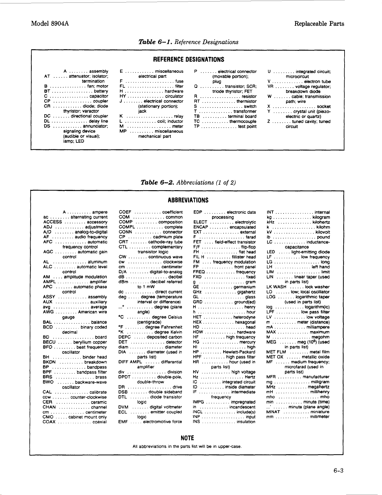
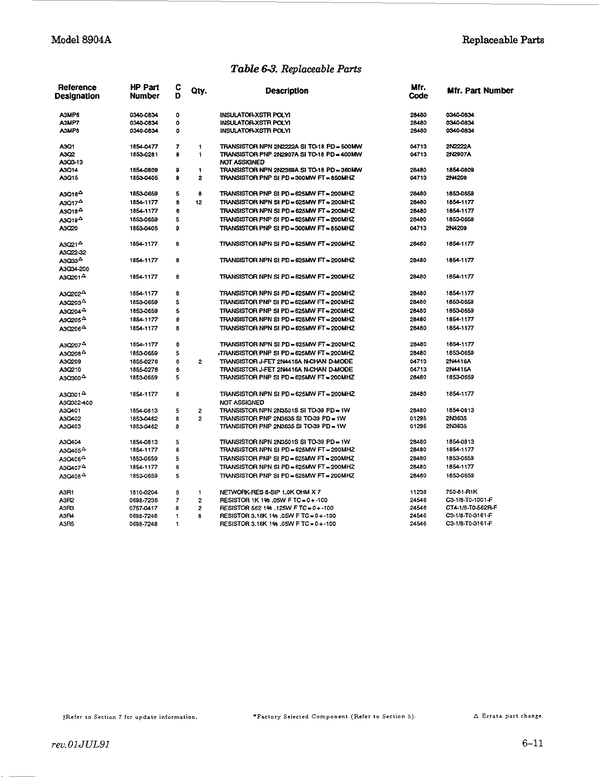
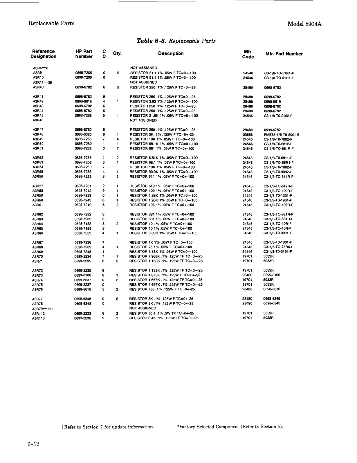
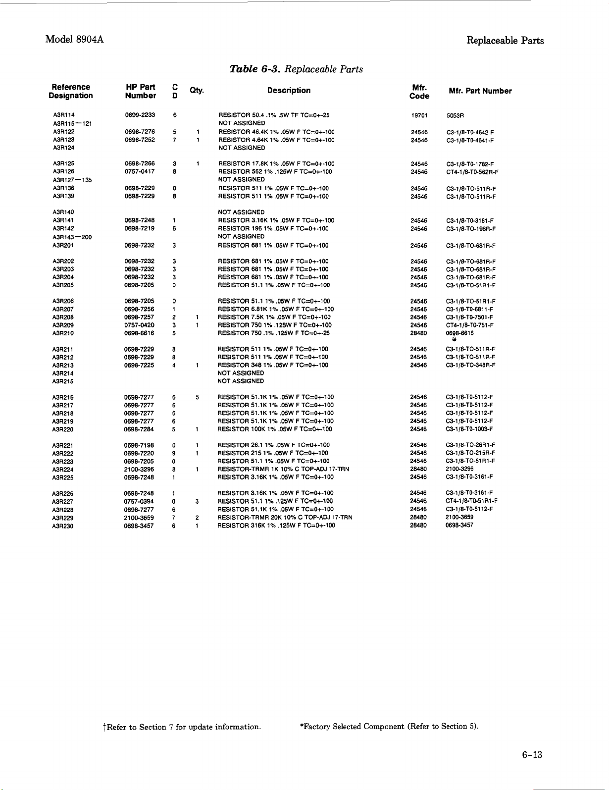
This section contains information for ordering parts. Table 6- 1 lists reference designations, and
Table 6-2 lists abbreviations that are used in the Replaceable
parts in the instrument. Table 6-4 contains the names and addresses that correspond
manufacturer’s code numbers listed in Table 6-3.
in identifying and ordering chassis mounted parts and mechanical parts.
6-2.
REFERENCE DESIGNATIONS AND ABBREVIATIONS
Table 6-1 lists the reference designation letters
designations found in Table 6-1 are coupled with numeric designations to provide a unique reference
designation for each part in the instrument.
particular resistor
Table 6-2 lists abbreviations used in the parts list and on schematics.
6-3.
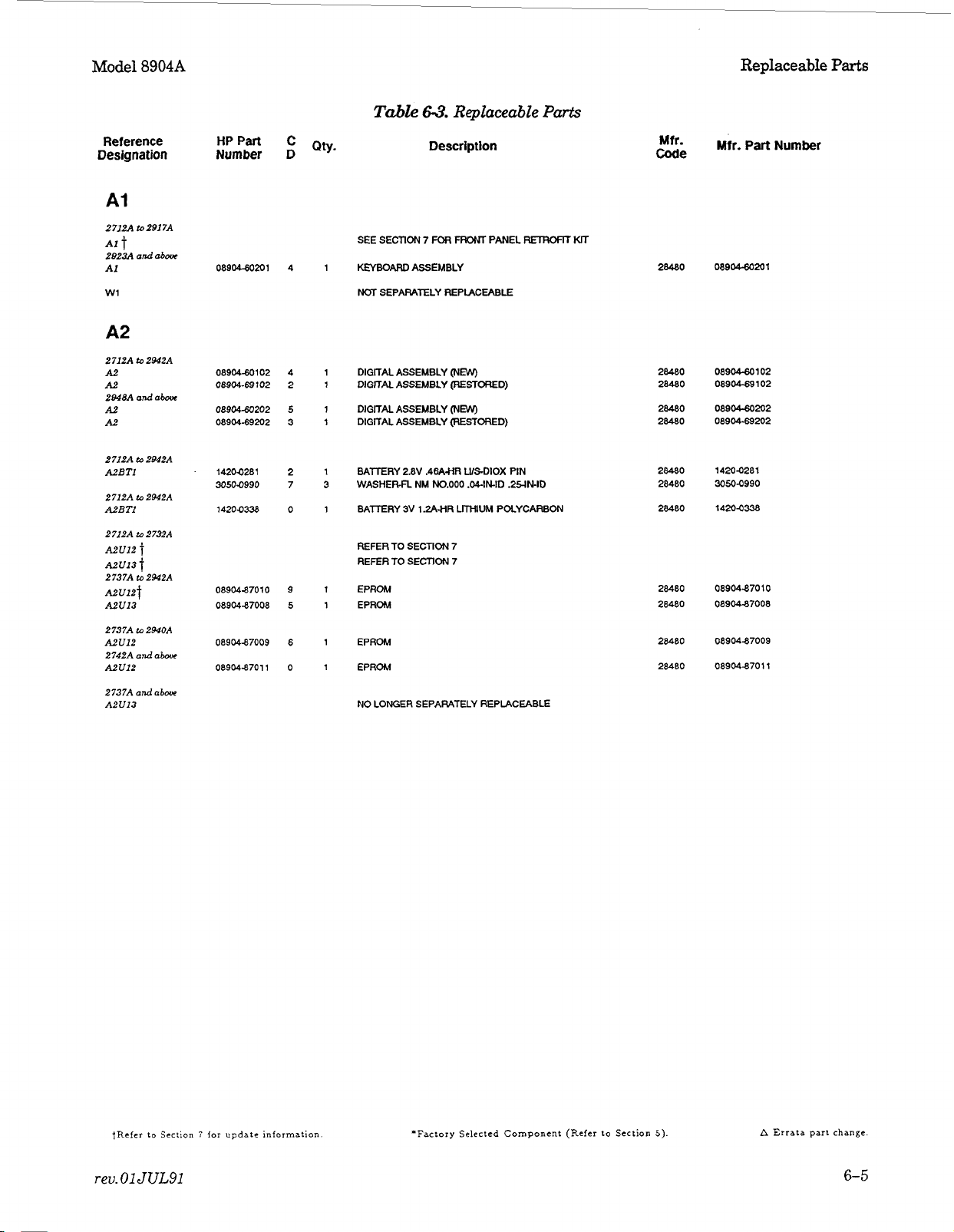
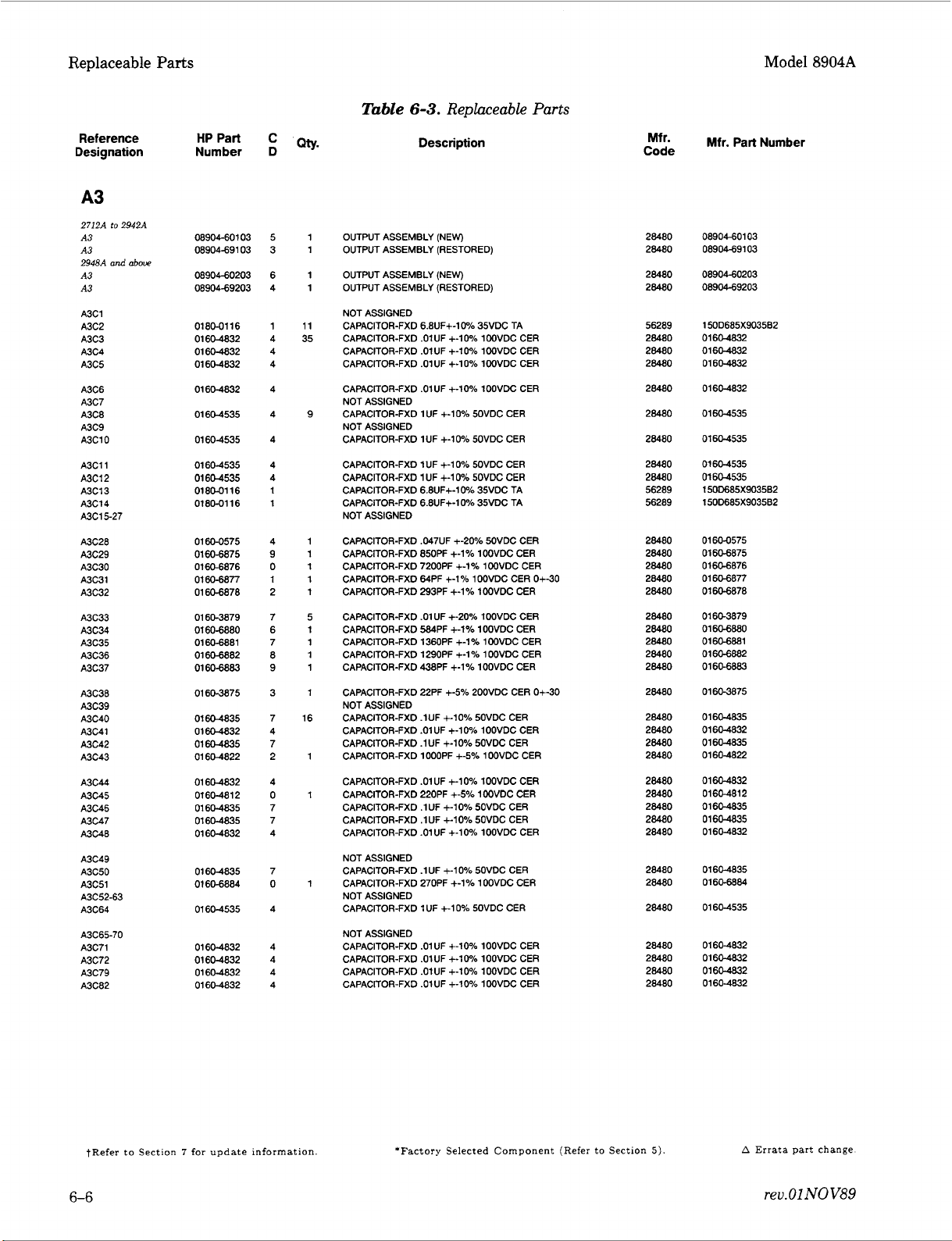
REPLACEABLE PARTS LIST
R1
on assembly A3. Designators with no letter are mechanical parts.
For
6
Parts
List. Table 6-3 lists all replaceable
Also
included in this section are drawings to aid
USED
for
electrical
example A3R1
IN
THIS
parts
in the instrument. The letter
is
the reference designation
MANUAL
to
the
of
a
Table 6-3 is a list
a. Electrical assemblies and their components with reference designations in alphanumeric order.
b. Chassis-mounted parts with reference designations in alphanumeric order.
c. Mechanical parts with reference designations
Ordering
Parts.
Instrument Serial Numbers.
Attached to the rear
are the instrument serial-number prefix. The last five digits (serial-number suffix) are unique to each
instrument. When parts in the instrument are changed, the serial-number prefix of the instrument may
also change. This means that sometimes a part will be listed more than once in the the replaceable
parts list along with a serial-number prefix
prefix on the serial plate of your instrument and order the part listed under the corresponding prefix
in the table. If no serial prefix information is listed, the part is compatible in instruments of all serial
numbers.
of
replaceable parts and is organized as follows:
in
numeric order.
of
the instrument is a serial-number plate. The first four digits and the letter
or
range of serial-number prefixes. Find the serial-number
NOTE
It is possible that some assemblies
or
(through service
serial-number prefixes later than that shown on
number tag. Be sure to note the printed circuit board number
being repaired
retrofitting) to reflect changes made to instruments with
or
replaced when ordering parts
in
your instrument have been updated
your
instrument serial-
for
your
instrument.
of
the
assembly
6-
1
Page 10
Replaceable
Parts
How
to
Order
Model
8904A
To order a part in the Replaceable
Have the following information ready
1.
The Hewlett-Packard
timely processing of your order.)
2.
The quantity required.
3.
An
approved purchase order number. (Sometimes required.)
Within the
Mater& Organization, RoseviUe, California.
for
information
part
USA,
Parts
List,
call
to
speed the ordering process:
number with the check
it
is
better to order directly
and
form
for
the uDirect Order Systems.
or write the nearest Hewlett-Packard Sales Office.
digit.
NOTE
Replaceable Parts List Updating (Manual Updates)
A
“MANUAL
current information available
addition pages which should be incorporated into the
Hewlett-Packard offers a Documentation Update Service
as
they become available.
recommend that
information, refer
Technical Writing Department
UPDATES‘ packet
If
you operate or service instruments
you
join this service immediately
to
the Documentation Update Service reply card included
is
at
the time of shipment. These packets consist of replacement and
(509) 922-4001,
shipped with the manual, when necessary,
manual
that
to
ensure that you
(The check
from
Ask
your
to
bring
will
provide you with further updates
of
different
manual
digit
the
HP
nearest
it
up
to
serial
will
ensure accurate and
Support
HP
office
to
provide the most
date.
prefixes, we strongly
is
kept current. For more
in
this
manual,
or calk
or
write:
Hewlett-Packard
Technical Writing Department
24001
Spokane, WA
6-4.
MECHANICAL AND CHASSIS PART LOCATIONS AND REFERENCE DESIGNATIONS
Most mechanical parts are identified in Figures
this section. To find the part number and description of
drawings, and then look up the item number in Table
Miscellaneous
E.
Mission
Parts
Company
-
TAF
C-34
99220
toward the end of Table
6-1
6-3).
to
6-6.
These
a
mechanical part,
6-3
(mechanical
figures
are located
find
part
numbers are listed under
the part
at
the end of
in
one of the
6-2
rev.15FEB88
Page 11
Model
8904A
Replaceable
Parts
A
AT
........
.
.....
attenuator; isolator;
.............
B
..
................
BT
.
..............
c
..
...............
CP
.
CR
.
...........
thyristor: varactor
......
DC
.
DL
.
,
..............
...........
DS
.
signaling device
(audible or visual);
lamp; LED
ac
........
ACCESS
ADJ
AID
AL
ALC
APC
ASSY
AUX
avg
AWG American wire
BAL
BCD
BD
BECU
BFO
BKDN
BP
BPF
BRS
BWO
CAL
ccw
CER
CHAN
cm
..............
CMO
COAX
alternating current
.........
............
........
..............
.........
control
amplitude modulation
...........
.......
control
............
..............
. .....
...............
..........
decimal
.................
......
.........
..........
..............
.........
................
.......
oscillator
..............
.......
counter-clockwise
..............
.............
.....
cabinet mount only
..............
assembly
termination
fan: motor
battery
capacitor
coupler
diode; diode
directional coupler
delay line
annunciator:
accessory
adjustment
analog-to-digital
aluminum
automatic level
amplifier
automatic phase
assembly
auxiliary
average
balance
binary coded
beryllium copper
backware-wave
board
beat frequency
breakdown
bandpass
bandpass filter
brass
calibrate
ceramic
channel
centimeter
coaxial
nable
REFERENCE DESIGNATIONS
E
............
F
....................
FL
...................
................
H
...............
HY
J
........
K
...................
L
.............
..................
M
..........
MP
miscellaneous
electrical part
electrical connector
(stationary portion);
jack
miscellaneous
mechanical part
Table
COEF
...........
COM
.............
COMP
.........
COMPL
...........
CONN
...........
CP
..........
CRT
.......
CTL
.........
CW
........
..............
cw
..............
cm
........
D/A
dB
.................
dBm
........
dc
............
deg
.....
...'
...........
OC
..........
........
OF
OK
...........
DEPC
DET
..............
diam
..............
.......
DIA
DlFF
AMPL
div
................
..........
DPDT
DR
..................
DSB
.......
........
DTL
DVM
.......
........
ECL
EMF
.....
cadmium plate
cathode-ray tube
complementary
transistor logic
continuous wave
digital-to-analog
decibel referred
to 1 mW
direct current
degree (temperature
interval or difference)
degree (plane
angle)
degree Celsius
(centigrade)
degree Fahrenheit
.....
degree Kelvin
deposited carbon
diameter (used in
parts list)
......
amplifier
double-throw
double sideband
diode transistor
logic
digital voltmeter
emitter coupled
logic
electromotive force
6-1.
Reference Designations
P
.......
fuse
filter
hardware
circulator
relay
coil; inductor
meter
6-2.
Q
..........
R
.................
RT
S
..................
..............
T
TB
TC
TP
...............
Abbreviations
ABBREVIATIONS
coefficient
common
composition
complete
connector
clockwise
centimeter
decibel
detector
diameter
differential
division
double-pole,
drive
EDP
ELECT
ENCAP
EXT
F
...................
FET
FM
FP
FREQ
FXD
g
...................
.............
GE
GHz
GL
..................
GRD
....
H
....
h
HET
HEX
HD
IiF
..........
HG
...................
HI
.........
HP
HPF
HR
HV
..................
Hz
IC
.........
..........
ID
IF
.............
IMPG
............
in
INCL
INP..
INS
electrical connector
(movable portion);
Plug
transistor; SCR;
triode thyristor; FET
..............
..........
...........
(1
.........
processing
..........
........
...............
....
field-effect transistor
....
frequency modulation
.............
............
.................
............
............
._ . .
.............
..................
...............
.........
...........
............
..............
Hewlett-Packard
parts list)
integrated circuit
frequency
..........
.............
................
resistor
thermistor
switch
transformer
terminal board
thermocouple
test point
of
2)
electronic data
electrolytic
encapsulated
external
.......
flip-flop
front panel
frequency
gram
germanium
.gigahertz
glass
ground(ed)
......
henry
.......
heterodyne
hexagonal
head
high frequency
mercury
high pass filter
hour (used in
high voltage
Hertz
inside diameter
intermediate
impregnated
incandescent
include(s)
input
insulation
farad
fixed
hour
high
U
.........
V
.............
VR
........
.......
W
X
..................
Y
........
2
........
INT
................
................
kg
k
..................
.................
kV
..................
Ib
.............
LC
LED
LH
...............
LIM
.......
LIN
LK WASH
LO
......
LOG
log
'
LPF
LV
.
m
..........
.............
mA
MAX
M
................
MEG
MET FLM
MET
OX
......
MF
...............
mg
mH
..............
mho
...........
min
..........
MlNAT
..............
mm
integrated circuit;
microcircuit
voltage regulator;
breakdown
cable: transmission
path; wire
crystal unit (piezo-
electric or quartz)
tuned cavity; tuned
circuit
capacitance
.....
light-emitting diode
..................
linear taper (used
in parts list)
......
low;
.......
local
logarithmic taper
(used in parts list)
...
.
low pass filter
...
meter (distance)
.............
.......
meg
in parts list)
........
......
metallic oxide
medium frequency;
microfarad (used
manufacturer
.................
minute (plane angle)
...........
electron tube
diode
socket
internal
kilogram
kilohm
kilovolt
pound
inductance-
left
hand
limit
lock washer
oscillator
lcgarithm(ic)
low voltage
milliampere
maximum
megohm
(lo6)
(used
metal film
in
milligram
millihenry
mho
minute (time)
miniature
millimeter
All abbreviations
NOTE
in
the parts list will
b%
in upper-case.
6-3
Page 12
Replaceable
MOM
mV
mVac
mVpp
mVrms
mW
MUX
MY
&
pF
pH
pV
pVac
pVdc
@Vpk
pVp-p
pvrms
pW
N/O
NOM
NORM
NPN negative-positive-
NPO
NRFR
NSR
ns
nW
OBD
Parts
MOD
....
...........
device)
................
...........
.......
to-peak
.........
...............
.............
.................
............
..............
.............
...............
..........
..........
........
..............
..........
..............
.......
.........
.............
.....
....
microvolt. peak
.......
microvolt, peak-
to-peak
........
.............
negative-positive
zero (zero temperature coefficient)
.....
not recommended
for field replacement
replaceable
order by description
modulator
momentary
millivolt
millivolt, ac
millivolt, peak-
millivolt, rms
milliwan
multiplex
mylar
microampere
microfarad
microhenry
microvolt
microvolt, ac
microvolt, dc
microvolt, rms
microwatt
normally open
nominal
normal
not separately
nanosecond
...
nanowatt
Table
6-2.
OD
........
OH
..............
OP AMPL
OX..
outside diameter
.......
amplifier
operational
.........
.......
................
......
peak
(used
........
PAM
...........
PC
PCM
PDM
.........
pF ...............
PH
BRZ
PHL
...............
PIN
........
PLO
....
PM
.......
PNP
P/O
................
POLY
PORC
. , . , .
POS
POSN
p-p
...........
PPM
PREAMPL
PRF
........
PRR
ps
.............
..................
PT
PTM
PWM
pulse-amplitude
modulation
....
......
..........
............
.............
.........
....
printed circuit
pulse-code modulation; pulse-count
modulation
pulse-duration
modulation
....
phosphor bronze
positive-intrinsic-
negative
phase lock oscillator
phase modulation
positive-negative-
positive
polystyrene
positive: position(s)
(used in parts list)
peak-to-peak
in parts list)
pulse-position
modulation
......
preamplifier
pulse-repetition
frequency
pulse repetition rate
picosecond
............
modulation
...........
modulation
pulse-width
Abbreviations
oval head
option
oscillator
oxide
ounce
in parts
picofarad
Phillips
ltage
peak
lock
part of
porcelain
position
point
pulse-time
(2
of
2)
RECT
..............
REG
.............
..........
REPL
RH
RLC
RMO
rms
RND
ROM
R&P
RWV
S
S
...
S-B
SCR
SE
SECT
SI
SIL..
SL
SNR
SPDT
SPG
SR
SPST single-pole,
SS ...........
SSB
STL
SWR
SYNC
T
TA tantalum
TC
interference
...
round head; right hand
.............
inductancecapacitance
.......
.......
root-mean-square
................
.....
read-only memory
.........
.......
voltage
........
(used
.......
silicon controlled
rectifier; screw
...............
.............
..................
................
...................
....
signal-to-noise ratio
..........
double-throw
................
...............
........
.........
....
standing-wave ratio
..........
.....
timed (slow-blow fuse)
............
compensating
rectifier
....
reference
regulated
replaceable
resistance-
rack mount only
round
rack and panel
reverse working
ng parameter
second (time)
(plane angle)
slow-blow (fuse)
in
parts list)
selenium
sections
silicon
silver
slide
single-pole,
spring
splitring
W
Service Sheet
single sideband
synchronize
temperature
Model
TD
..............
.............
TERM
TFT
......
................
TGL toggle
THD
................
THRU
.............
.................
TI
TOL
.............
TTL
.....
transistor-transistor
N
TVI
TWT
U
UF
UHF
UNDEF
UNFEG
v
VA
Vac
VAR
VCO
Vdc
VDCW
VHF
Vrms
VSWR
VTO
VTVM
V(X)
w..
wl
WIV
WW
W/O
logic
...............
....
television interference
.....
traveling wave tube
........
in
parts list)
......
microfarad (used in
parts list)
.....
ultrahigh frequency
..........
........
.....................
.............
...............
...............
......
oscillator
...............
.....
(used
oscillator
.....
very-high frequency
............
......
wave ratio
...........
oscillator
.........
voltmeter
.........
..................
...................
........
voltage
............
...............
YIG
......
Z,
...........
impedance
time delay
thin-film transistor
micro (used
voltage-controlled
volts, dc, working
yttrium-iron-garnet
terminal
thread
through
titanium
tolerance
television
undefined
unregulated
volt
voltampere
volts, ac
variable
volts, dc
in
parts list)
volts, rms
voltage standing
voltage-tune
vacuum-tube
volts, switched
working inverse
characteristic
wan
with
wirewound
without
8904A
6-4
NOTE
All abbreviations in the parts list will
MULTIPLIERS
Abbreviation
T
G
M
k
da
d
C
m
P
n
P
f
a
Prefix
tera
gigs
mega
kilo
deka
deci
centi
milli
micro
nano
pic0
femto
ano
be
in
upper-case.
Multiple
10’2
1
09
1
06
103
10
10-1
10-2
10-3
10-6
10-9
10-12
10-’5
10-18
Page 13
Model
8904A
ReplaceabIe
Parts
Reference
Designation
A1
2
71ZA
to
291
7A
Alt
2025%
and abwo
AI
w1
A2
2712A
to
2942A
A2
A2
2048A and ah
A2
A2
2712A
to
2M2A
A2BTl
2712A
to
2942A
A2BTl
2
712A
to
2
732A
A2u12
i.
A2U13
t
2737A
to
2942A
AZUlZt
A2U13
2737A
to
294OA
A2u12
2742A
and ah
A2u12
2737A
andabwo
A2U13
HPPart
Number
08904-60201 4 1
0890480102 4 1
08904-69102 2
08904-60202
08904-89202
14200281
3050.0990
14200238
0890487010 9 1
0~90487008
0890487009
0890487011
C
D
5
3
2
7
0
5
6
0
Qty.
SEE SECTION
KEYBOARD
NOT
DIGITAL ASSEMBLY
DIGITAL ASSEMBLY
1
1
DIGITAL ASSEMBLY
DIGITAL ASSEMBLY
1
BA'ITERY
1
WASHERFL NM
3
BAlTERY
1
REFER
REFER
EPROM
EPROM
1
EPROM
1
EPROM
1
NO
Table
63'.
Replaceable Parts
Description
7
KXI
FRONT
PANEL
RETRoFlT
ASSEMBLY
SEPARATELY REPLACEABLE
(NW
(RESTORED)
(NEW)
(RESTORED)
2.8V
.46A%IR
US-DIOX
.WlN-ID
PIN
.25-IN-ID
NO.000
3V
1.2AHR
LMIUM POLYCARBON
TO
SECTION
SECTION
7
7
TO
LONGER SEPARATELY REPLACEABLE
WT
llfr-
Code
28480 08804-60201
28480 08904-60102
28480 089066Q102
28480 08904-60202
28480 08904-69202
28480 14200281
28480 30504990
28480 14204338
28480 0890487010
28480 08904-87008
28480 0890487009
28480 089048701 1
Mtr. Part Number
tRefer to Section
rev.
01
JUL91
i
for
update information
*Factory Selected Component
(Refer
to
Section
5).
A
Errata part change.
6-5
Page 14
Replaceable Parts
Model
8904A
Reference
Designation
A3
2712A
to
2942A
A3
A3
and
2948A
A3
A3
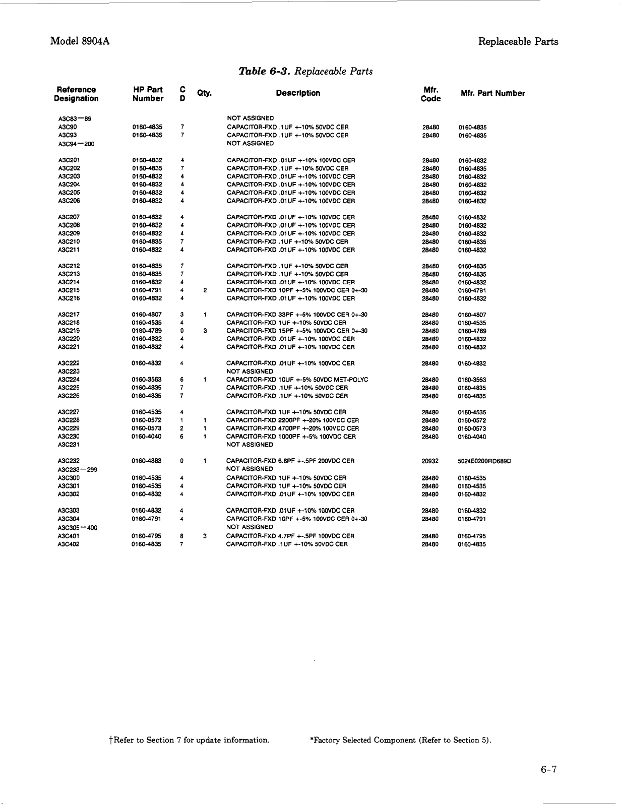
A3C1
A3C2
A3C3
A3C4
A3C5
A3C6
A3C7
A3C8
A3C9
A3C10
A3C11
A3C12
A3C13
A3C14
A3C15-27
A3C28
A3C29
A3C30
A3C31
A3C32
A3C33
A3C34
A3C35
A3C36
A3C37
A3C38
A3C39
A3C40
A3C41
A3C42
A3C43
A3C44
A3C45
A3C46
A3C47
A3C48
A3C49
A3C50
A3C51
A3C52-63
A3C64
A3C65-70
A3C71
A3C72
A3C79
A3C82
abow
HPPart C
Number
08904-60103
08904-69103 3
0890440203
08904-69203 4
01804116
0160-4832 4 35
0160-4832 4
0160-4832 4
0160-4832 4
0160-4535 4
01604535 4
0160-4535 4
0160-4535 4
01804116
01804116
01600575 4
0160-6875 9
0160-6876
0160-6877
0160-6878
0160-3879 7 5
0160-6880
0160-6881 7
0160-6882
0160-6883 9
0160-3875 3
0160435 7 16
0160-4832 4
0160-4835 7
0160-4822
0160-4832 4
0160-4812
0160-4835 7
01604835 7
01604832 4
0160-4835 7
01606884
0160-4535 4
01604832 4
0160-4832 4
0160-4832 4
0160-4832 4
Q~.
D
5
6
1
11
1
1
0
1
2
6
8
2
0
0
fible
6-3.
Replaceable
Description
OUTPUT ASSEMBLY (NEW)
1
OUTPUT ASSEMBLY (RESTORED)
1
OUTPUT ASSEMBLY (NEW)
1
OUTPUT ASSEMBLY (RESTORED)
1
NOT ASSIGNED
CAPACITOR-FXD 6.8UF+-10% 35VDC TA
CAPACITOR-FXD .OlUF
CAPACITOR-FXD .OlUF
CAPACITOR-FXD .OlUF +-lo%
CAPACITOR-FXD .OlUF
NOT ASSIGNED
CAPACITOR-FXD 1UF +-10% 50VDC CER
9
NOT ASSIGNED
CAPACITOR-FXD 1UF +-1O% 5OVDC CER
CAPACITOR-FXD 1UF +-lo% 50VDC CER
CAPACITOR-FXD 1 UF +-lo% 50VDC CER
CAPACITOR-FXD 6.8UF+-10°/o 35VDC TA
CAPACITOR-FXD 6.8UF+-10% 35VDC TA
NOT ASSIGNED
CAPACITOR-FXD .047UF
1
CAPACITOR-FXD 850PF +-1% 100VDC CER
1
CAPACITOR-FXD 7200PF +-1%
1
CAPACITOR-FXD 64PF +-1% 1 OOVDC CER
1
CAPACITOR-FXD 293PF +-1% 1WVDC CER
1
CAPACITOR-FXD .OlUF
CAPACITOR-FXD 584PF
1
CAPACITOR-FXD 1360PF +-1%
1
CAPACITOR-FXD 129OPF +-1%
1
CAPACITOR-FXD 438PF +-1% 100VDC CER
1
CAPACITOR-FXD 22PF +-5% POOVDC CER 0+-30
1
NOT ASSIGNED
CAPACITOR-FXD .1UF +-10% 5OVDC CER
CAPACITOR-FXD .OlUF +-10% 100VDC CER
CAPACITOR-FXD .1UF +-lo% 50VDC CER
CAPACITOR-FXD lOOOPF
1
CAPACITOR-FXD .OlUF t10% 1 WVDC CER
CAPACITOR-FXD 220PF +-5% 1WVDC CER
1
CAPACITOR-FXD .1UF +-lo% 5OVDC CER
CAPACITOR-FXD .1UF +-lo% 50VDC CER
CAPACITOR-FXD .OlUF +-lo% 100VDC CER
NOT ASSIGNED
CAPACITOR-FXD
CAPACITOR-FXD 270PF +-1%
1
NOT ASSIGNED
CAPACITOR-FXD
NOT ASSIGNED
CAPACITOR-FXD .OlUF
CAPACITOR-FXD .OlUF
CAPACITOR-FXD
CAPACITOR-FXD .OlUF +-lo% 1 WVDC CER
+-1O%
+-loo/.
+-1oO/c
+-20%
+-20%
+-1%
+-5%
.1
UF +-lo% 5OVDC CER
1
UF +-lo% 50VDC CER
+-loo/.
+-1O%
.OWF
+-io%
lWVDC CER
lWVDC CER
1
WVDC CER
lOOVDC CER
5OVDC CER
1
WVDC CER
1WVDC CER
100VDC CER
1
WVDC CER
1
WVDC CER
lOOVDC CER
1
WVDC CER
lOOVDC CER
lOOVDC CER
IOOVDC
CER
Parts
0+30
Mfr-
Code
28480
28480
28480
28480
56289
28480
28480
28480
28480
28480
28480
28480
28480
56289
56289
28480
28480
28480
28480
28480
28480
28480
28480
28480
28480
28480
28480
28480
28480
28480
28480
28480
28480
28480
28480
28480
28480
28480
28480
28480
28480
28480
Mfr. Part Number
08904-60103
08904-69103
08904-60203
08904-69203
150D685X903562
01 60-4832
01604832
60-4832
01
01 604832
0160-4535
0160-4535
0160-4535
0160-44535
150D685X9035B2
150D685X903562
01 60-0575
01606875
01606876
01 60-6877
0160-6878
0160-3879
60-6880
01
0160-6881
01 60-6882
01 60-6883
01604875
01 60-4835
01 60-4832
01 60-4835
01 60-4822
0160-4832
01604812
01604835
0160-4835
0160-4832
01604835
01 60-6884
01 60-4535
0160-4832
01 60-4832
01 60-4832
01 60-4832
?Refer to Section 7 for update information.
6-6
'Factory Selected Component (Refer to Section
5).
A
Errata part change
reu.OlNOV89
Page 15
Model
8904A
Replaceable
Parts
Reference
Designation
A3C83-89
A3C90
A3C93
A3c94-200
A3C201
A3c202
Ax203
Ax204
A3C205
A3C206
Ax207
A3c208
A3c209
A3C210
A3c211
A3c212
A3C213
A3C214
A3C215
Ax216
A3C217
A3C218
A3C219
A3C220
A3c221
A3C222
A3C223
A3C224
A3C225
A3C226
A3c227
A3C228
A3C229
A3C230
A3C231
A3C232
A3C233-299
A3C300
A3c301
A3C302
A3C303
A3c304
A3C305-400
A3C401
A3C402
HP Part
Number
01604835
01604B35
01 604832
01 604835
01 60-4832
01 60-4832
01 604832
01 60-4832
01 604832
01 604832
01 604832
01 60-4835
01 604832
01 60-4835
01
6c-4635
01 604832
0160-4791
01 60-4832
01 60-4807
01 60-4535
01 604789
01 604832
01 604832
01 60-4832
01609563
0160-4835
01 60-4835
01 604535
0160-0572
0160-0573
01 604040
01 60-4383
01604535
01 60-4535
01 604832
01604832
01 60-4791
01 60-4795
01604835
C
D
8
7
Table
7
7
NOT ASSIGNED
CAPACITOR-FXD .1UF +-lo% 50VDC CER
CAPACITOR-FXD .1UF +-1O% 5OVDC CER
NOT ASSIGNED
CAPACITOR-FXD .OlUF +-lo% lWVDC CER
CAPACITOR-FXD .1 UF +-1O% 5OVDC CER
CAPACITOR-FXD .OlUF +-lo% 1 WVDC CER
CAPACITOR-FXD .OlUF
CAPACITOR-FXD .OlUF +-lo% 1WVDC CER
CAPACITOR-FXD .OlUF +-lo% lWVDC CER
CAPACITOR-FXD .01 UF +-1O% 1 WVDC CER
CAPACITOR-FXD .OlUF +-1O% 100VDC CER
CAPACITOR-FXD .OlUF +-1O% lOOVDC CER
CAPACITOR-FXD .1 UF +-IO% 5OVDC CER
CAPACITOR-FXD .OlUF +-loo/. 1OOVDC CER
CAPACITOR-FXD .1 UF +-10% 5OVDC CER
CAPACITOR-FXD .1UF +-lo% 5OVDC CER
CAPACITOR-FXD .OlUF +-1O% 1 OOVDC CER
CAPACITOR-FXD 1OPF +-5% 1OOVDC CER
2
CAPACITOR-FXD .OlUF
1
CAPACITOR-FXD 33PF +-5% l00VDC CER
CAPACITOR-FXD 1UF +-1O% 5OVDC CER
CAPACITOR-FXD 15PF +-5% 1WVDC CER
3
CAPACITOR-FXD .01 UF +-lo% lOOVDC CER
CAPACITOR-FXD .OlUF +-lo% lOOVDC CER
CAPACITOR-FXD .OlUF
NOT ASSIGNED
1
CAPACITOR-FXD lOUF +-5% 50VDC MET-POLYC
CAPACITOR-FXD .1 UF +-lo% 50VDC CER
CAPACITOR-FXD .1UF +-lo% 50VDC CER
CAPACITOR-FXD 1UF
CAPACITOR-FXD 22OOPF +-20% 100VDC CER
CAPACITOR-FXD 4700PF +-20% lWVDC CER
CAPACITOR-FXD 1OOOPF +-5% lWVDC CER
NOT ASSIGNED
1
CAPACITOR-FXD 6.8PF +-.5PF 2OOVDC CER
NOT ASSIGNED
CAPACITOR-FXD 1 UF +-lo% 5OVDC CER
CAPACITOR-FXD 1UF +-loo/. 50VDC CER
CAPACITOR-FXD .OlUF +-lo% lOOVDC CER
CAPACITOR-FXD
CAPACITOR-FXD lOPF +-5% lOOVDC CER 0+-30
NOT ASSIGNED
CAPACITOR-FXD 4.7PF +-.5PF 100VDC CER
3
CAPACITOR-FXD .1 UF +-lo% 5OVDC CER
6-3.
Replaceable Parts
Description
+-lo"/.
lMWDC CER
+-loo/.
lOOVDC CER
+-lo%
lOOVDC CER
+-1O%
5OVDC CER
.OlUF
+-IO%
1OOVDC CER
0+30
0+30
0+30
Mfr*
Code
28480
28480
28480
28480
28480
28480
28480
28480
28480
28480
28480
28480
28480
28480
28480
28480
28480
28480
28480
28480
28480
28480
28480
28480
28480
28480
28480
28480
28480
28480
28480
20932
28480
28480
28480
28480
28480
28480
28480
Mfr. Part Number
0160-4835
0160-4835
01 60-4832
01604835
0160-4832
01 604832
01 60-4832
0160-4832
01 60-4832
01 60-4832
0160-4832
0160-4835
01 60-4832
01 60-4835
01 60-4835
0160-4832
0160-4791
01 €0-4832
0160-4807
01 60-4535
01 60-4789
01 60-4832
01 60-4832
01
60-4832
01 60-3563
0160-4835
0160-4835
01 604535
0160-0572
01 60-0573
0160-4040
5024E0200RD689D
01 60-4535
01 60-4535
0160-4832
01604832
0160-4791
0160-4795
0160-4835
?&fer to Section 7 for
update
information. *Factory Selected Component (Refer
to
Section
5).
6-7
Page 16
Replaceable
Parts
Model
8904A
Reference
Designation
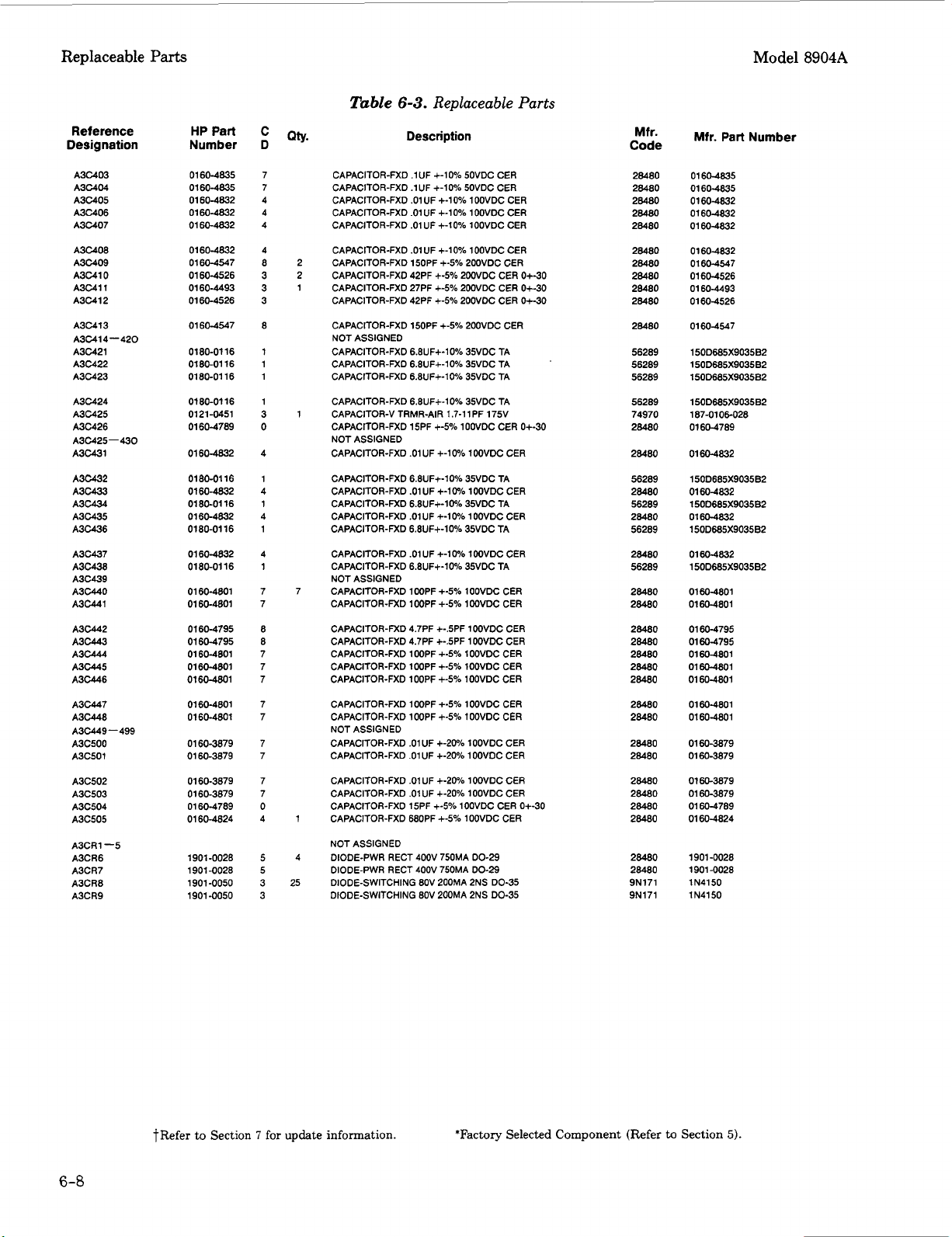
A3C403
A3C404
A3C405
A3C406
A3C407
A3C408
A3C409
A3C410
1
A3C41
A3C412
A3C413
A3C414-420
A3C421
A3C422
A3C423
A3C424
A3C425
A3C426
A3C425-430
A3C431
A3C432
A3C433
A3C434
A3C435
A3C436
A3C437
A3C438
AX439
A3C440
MC441
A3W2
A3C443
A30614
A3C445
A3C446
A3C447
A3C448
A3C449-499
AX500
A3C501
A3C502
AX503
AX504
AX505
A3CR1-5
A3CR6
A3CR7
A3CR8
A3CR9
HP Part
Number
01
60-4835
01 60-4835
01 60-4832
60-4832
01
01
60-4832
0160-4832
0160-4547
01 60-4526
0160-4493
0160-4526
01 60-4547
0180-0116
16
01 80-01
0180-0116
01 80-01 16
0121-0451
01 60-4789
01
60-4832
0180-0116
01604832
01 80-01 16
01 60-4832
0180-01 16
01 60-4832
16
0180-01
01604801
01 60-4801
01604795
01 60-4795
01 60-4801
0160-4801
0160-4801
01 604801
01 60-4801
01 60-3879
01 60-3879
01 60-3879
0160-3879
01 60-4789
01 60-4824
1901
-0028
1 901
-0028
1 901
-0050
1901 -0050
C
D
7
7
4
4
4
4
8
3
3
3
8
1
1
1
1
3
0
4
1
4
1
4
1
4
1
7
7
8
8
7
7
7
7
7
7
7
7
7
0
4
5
5
3
3
Table
QW.
CAPACITOR-FXD .1UF
CAPACITOR-FXD .1UF +-lo% 5OVDC CER
CAPACITOR-FXD .OlUF +-lo% 100VDC CER
CAPACITOR-FXD .OlUF +-lo% lOOVDC CER
CAPACITOR-FXD .OlUF +-lo% lOOVDC CER
CAPACITOR-FXD .OlUF +-lo% lOOVDC CER
2
CAPACITOR-FXD 150PF +-5% ZOOVDC CER
2
CAPACITOR-FXD 42PF +-5% POOVDC CER
1
CAPACITOR-FXD 27PF +-5% ZOOVDC CER
CAPACITOR-FXD 42PF +-5% ZOOVDC CER
CAPACITOR-FXD 150PF +-5% POOVDC CER
NOT ASSIGNED
CAPACITOR-FXD 6.8UF+-1Oo/o 35VDC TA
CAPACITOR-FXD 6.8UF+-1O0/- 35VDC TA
CAPACITOR-FXD 6.8UF+-llW 35VDC TA
CAPACITOR-FXD 6.8UF+-10°/e 35VDC TA
1
CAPACITOR-V TRMR-AIR 1.7-1 1PF 175V
CAPACITOR-FXD 15PF +-5% lOOVDC CER
NOT ASSIGNED
CAPACITOR-FXD .OlUF +-10% lOOVDC CER
CAPACITOR-FXD 6.8UF+-1Oo/o 35VDC TA
CAPACITOR-FXD .OlUF +-lo% lOOVDC CER
CAPACITOR-FXD 6.8UF+-10% 35VDC TA
CAPACITOR-FXD .OlUF
CAPACITOR-FXD 6.8UF+-1Oo/o 35VDC TA
CAPACITOR-FXD .OlUF
CAPACITOR-FXD 6.8UF+-1Oo/o 35VDC TA
NOT ASSIGNED
7
CAPACITOR-FXD lOOPF +-5% lOOVDC CER
CAPACITOR-FXD 1OOPF +-5% lOOVDC CER
CAPACITOR-FXD 4.7PF +-SPF 1 OOVDC CER
CAPACITOR-FXD 4.7PF +-.5PF 1 OOVDC CER
CAPACITOR-FXD lOOPF +-5% lOOVDC CER
CAPACITOR-FXD lOOPF
CAPACITOR-FXD 1OOPF +-5% lOOVDC CER
CAPACITOR-FXD lOOPF
CAPACITOR-FXD lOOPF +-5% 1OOVDC CER
NOT ASSIGNED
CAPACITOR-FXD .OlUF
CAPACITOR-FXD .OlUF
CAPACITOR-FXD .OlUF
CAPACITOR-FXD .OlUF
CAPACITOR-FXD 15PF
1
CAPACITOR-FXD 680PF +-5% lOOVDC CER
NOT ASSIGNED
4
DIODE-PWR RECT 400" 750MA DO-29
DIODE-PWR RECT 400V 750MA DO-29
DIODE-SWITCHING 8OV 200MA 2NS DO-35
25
DIODE-SWITCHING 8OV 200MA
6-3.
Description
Replaceable Parts
+-lo%
5OVDC CER
0+-30
0+-30
0+-30
0+-30
+-lo%
lOOVDC CER
+-10%
lOOVDC CER
+-5%
lOOVDC CER
+-5%
lOOVDC CER
+-2O%
lOOVDC CER
+-20%
lOOVDC CER
+-20%
lOOVDC CER
+-20%
100VDC CER
+-5%
lOOVDC CER
2NS
0+-30
DO-35
Mfr.
Code
28480
28480
28480
28480
28480
28480
28480
28480
28480
28480
28480
56289
56289
56289
56289
74970
28480
28480
56289
28480
56289
28480
56289
28480
56289
28480
28480
28480
28480
28480
28480
28480
28480
28480
28480
28480
26480
28480
28480
28480
28480
28480
9N171
9N171
Mfr. Part Number
01
60-4835
0160-4835
60-4832
01
0160-4832
60-4832
01
0160-4832
01604547
01 60-4526
01 60-4493
01604526
01604547
150D685X903562
150D685X903582
150D685X9035B2
150D685X903562
187-0106-028
0160-4789
01
60-4832
150D685X9035B2
01604832
150D685X903582
60-4832
01
150D685X903562
01604832
150D685X9035B2
0160-4801
0160-4801
01 60-4795
01604795
0160-4801
0160-4801
01 60-4801
01 604801
0160-4801
01 60-3879
01604879
01 60-3879
0160-3879
01 60-4789
01 60-4824
1901
-0028
1901
-0028
1
N4150
1
N4150
6-8
tRefer
to
Section
7
for
update information.
'Factory Selected Component (Refer
to
Section
5).
Page 17
Model
8904A
Replaceable
Parts
Reference
Designation
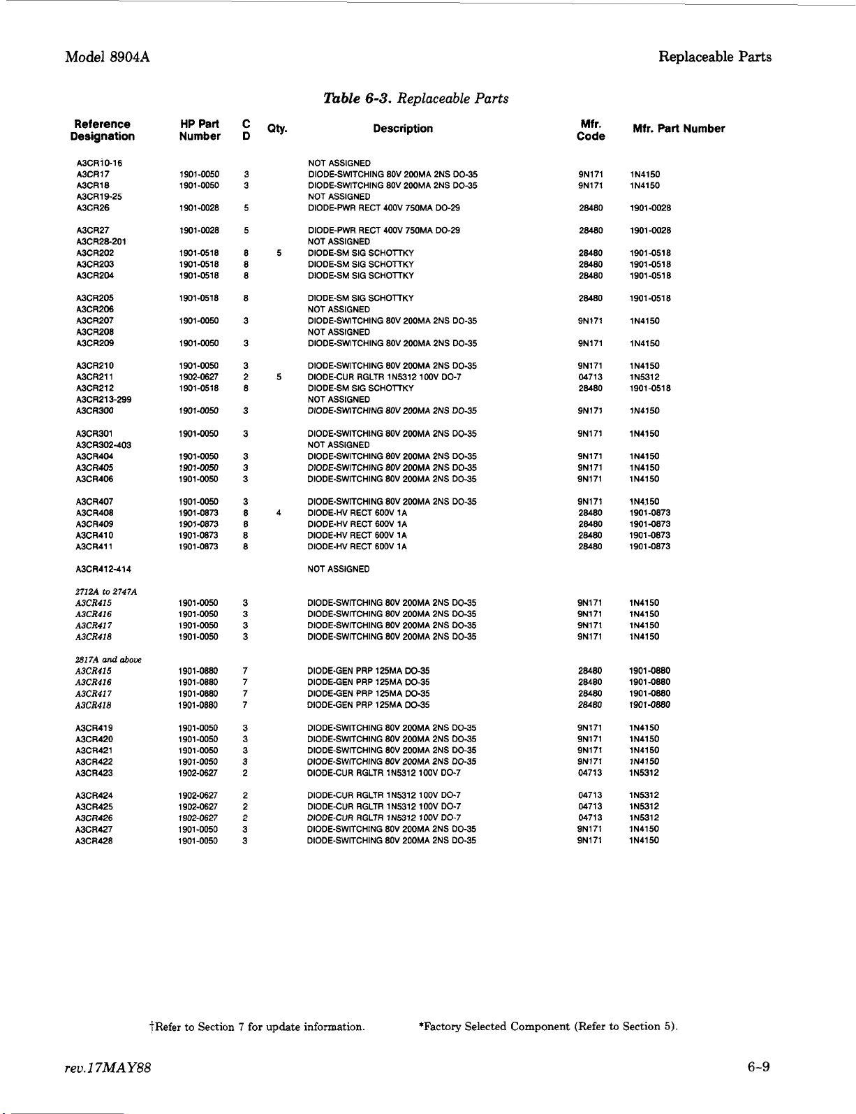
A3CRlO-16
A3CR17
MCRl8
A3CRl9-25
A3CR26
A3CR27
A3CR28-201
A3CR2M
A3CR203
A3CR204
A3CR205
A3CR206
A3CR207
A3CR208
A3CR209
A3CR210
A3CR211
A3CR212
A3CR213-299
A3CR300
A3CR301
A3CR302-403
A3CR404
A3CR405
A3CR406
A3CR407
A3CR408
A3CR409
A3CR410
A3CR411
A3CR412414
2712A
to
2747A
A3CR415
A3CR416
A3CR417
A3CR418
2817A
and
A3CR415
A3CR.116
A3CR417
A3CR416
A3CR419
A3CR420
A3CR421
A3CR422
A3CR423
A3C R424
A3CR425
A3CR426
A3CR427
A3CR428
above
HP
Part
Number
1901 -0050
1901
-0050
1901
-0028
1901
-0028
1901 -051
1901 -051
1901-0518
1901-0518
1901-0050
1901 -0050
1901-0050
1902-0627
1901-0518
1901-0050
1901-0050
1901-0050
1901-0050
1901-0050
1901 -0050
1901-0873
1901-0873
1901-0873
1901 -0873
1901 -0050
1901-0050
1901 -0050
1901-0050
1901 -0880
-0880
1901
1901 -0880
1901-0860
1901 -0050
1901 -0050
1901-0050
1901-0050
1902-0627
1902-0627
1902-0627
1902-0627
1901-0050
1901 -0050
C
Qty.
D
8
8
3
3
3
3
3
3
3
84
8
8
8
%Me
6-3.
Replaceable Parts
Description
NOT ASSIGNED
DIODE-SWITCHING 8OV 2WMA 2NS 00-35
DIODE-SWITCHING 8OV 200MA 2NS DO-35
NOT ASSIGNED
DIODE-PWR RECT 400V 750MA DO-29
DIODE-PWR RECT 400V 750MA DO-29
NOT ASSIGNED
5 DIODE-SM SIG SCHOTTKY
DIODE-SM SIG SCHOTTKY
DIODE-SM SIG SCHOTTKY
DIODE-SM SIG SCHOTTKY
NOT ASSIGNED
DIODE-SWITCHING 8OV 200MA 2NS DO-35
NOT ASSIGNED
DIODE-SWITCHING 8OV 200MA 2NS DO-35
DIODE-SWITCHING 8OV 200MA 2NS DO35
DIODE-CUR RGLTR 1N5312 1WV DO-7
5
DIODE-SM SIG SCHOTTKY
NOT ASSIGNED
DIODE-SWITCHING 8OV 200MA 2NS DO-35
DIODE-SWITCHING 8OV 200MA 2NS DO-35
NOT ASSIGNED
DIODE-SWITCHING 8OV 200MA 2NS DO35
DIODE-SWITCHING 8OV 200MA 2NS DO35
DIODE-SWITCHING 8OV 200MA 2NS DO35
DIODE-SWITCHING 8OV 200MA 2NS DO-35
DIODE-HV RECT WOV 1A
DIODE-HV RECT 600V 1A
DIODE-HV RECT 600V 1A
DIODE-HV RECT 600V 1A
NOT ASSIGNED
DIODE-SWITCHING 8OV 200MA 2NS DO35
DIODE-SWITCHING 8OV 200MA 2NS DO35
DIODE-SWITCHING
DIODE-SWITCHING 8OV 200MA 2NS DO35
DIODE-GEN PRP 125MA DO-35
DIODE-GEN PRP 125MA 00-35
DIODE-GEN PRP 125MA DO-35
DIODE-GEN PRP 125MA DO45
DIODE-SWITCHING 8OV 200MA 2NS DO-35
DIODE-SWITCHING 8OV 200MA 2NS DO35
DIODE-SWITCHING 8OV 200MA 2NS DO-35
DIODE-SWITCHING 8OV 200MA 2NS DO45
DIODE-CUR RGLTR 1N5312 1OOV DO-7
DIODE-CUR RGLTR 1N5312 1OOV DO-7
DIODE-CUR RGLTR 1N5312 1OOV DO-7
DIODE-CUR RGLTR 1NS312 lOOV DO-7
DIODE-SWITCHING 8OV 200MA 2NS DO35
DIODE-SWITCHING 8OV 200MA 2NS DO-35
8OV
200MA 2NS 00-35
Mfr*
Code
9N171 1N4150
9N171 1N4150
28480
28480
28480 1901 -051
28480
28480 1901 -051 8
Mfr. Part Number
1901-0028
1901-0028
1901-0518
28480 1901-0518
9N171 1N4150
9N171 1N4150
9N171 1N4150
04713 1N5312
28480 1901-0518
9N171 1N4150
9N171 1N4150
9N171 1N4150
9N171 1N4150
9N171 1N4150
9N171 1N4150
28480 1901-0873
28480 19014873
28480
28480 1901 -0873
9N171 1N4150
9N171 1N4150
9N171 1N4150
9N171 1N4150
28480 1901
28480
28480 1901-0880
28480 1901-0880
9N171 1N4150
9N171 1N4150
9N171 1N4150
9N171 1N4150
04713 1N5312
04713 1N5312
04713 1N5312
04713 1N5312
9N171 1N4150
9N171 1N4150
19014873
-0880
1901-0880
8
rev.
1
7MAY88
thfer to Section 7 for update information.
*Factory Selected Component (Refer
to
Section
5).
6-9
Page 18
Replaceable Parts Model
8904A
Reference
Designation
A3CR429
A3CR430
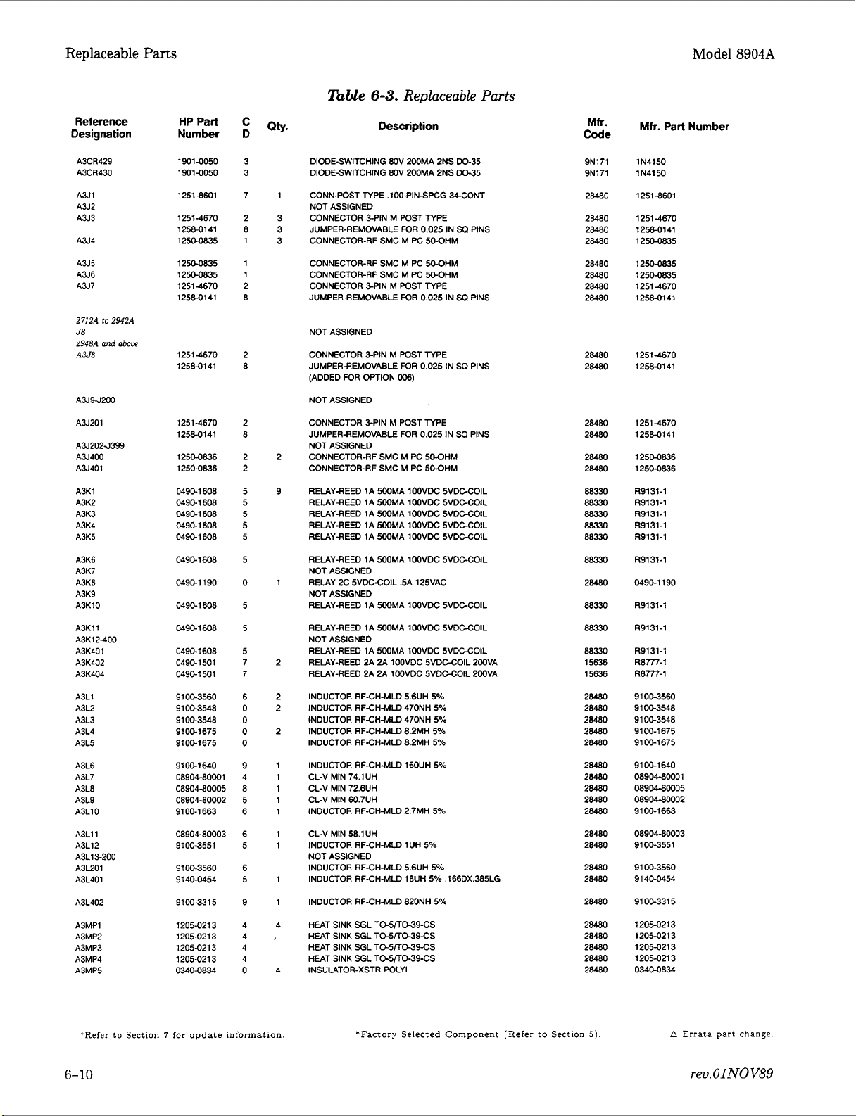
A31
A32
A33
A34
A35
A36
A37
2712A
to
2942A
J8
and
2948A
A3J8
A394200
A3201
A3202J399
A3400
A3401
A3K1
A3K2
A3K3
A3K4
A3K5
A3K6
A3K7
A3K8
A3K9
A3K10
A3K11
A3K12-400
A3K401
A3K402
A3K404
A3L1
A3L2
A3L3
A3L4
A3L5
A3L6
A3L7
A3L8
A3L9
A3L10
A3L11
A3L12
A3L13-200
A3L201
A3L401
A3L402
A3MPl
A3MP2
A3MP3
A3MP4
A3MP5
abom
HP Part
Number
19010050
1901 -0050
12518601
1251-4670
12580141
1250-0835
1250-0835
1250-0835
12514670
12580141
1251-4670
12580141
12514670
12580141
1250-0836
12500836
0490-1 608
04901608
608
0490-1
0490-1 608
608
04901
0490-1608
0490-1 190
0490-1
608
0490-1 608
0490-1 608
0490-1501
0490-1501
91 00-3560
91 003548
9100-3548
9100-1675
9100-1675
91
00-1
640
08904-80001
08904-80005
08904-80002
9100-1 663
08904-80003
91003551
91003560
91 40-0454
91 00-331 5
1205-0213
1205-021
3
1205-021 3
1 205-021 3
03400834
C
D
5
5
5
5
5
0
5
5
5
7
7
6
0
0
0
0
9
4
8
5
6
6
5
6
5
9
4
4
4
4
0
3
3
7
2
8
1
1
1
2
8
2
8
2
8
2
2
5
Table
QW
DIODE-SWITCHING 8OV 200MA 2NS DO-35
DIODE-SWITCHING 80V 200MA 2NS DO45
1
CONN-POST TYPE ,100-PIN-SPCG WONT
NOT ASSIGNED
3
CONNECTOR SPIN M POST TYPE
JUMPER-REMOVABLE
3
CONNECTOR-RF SMC M PC 5WHM
3
CONNECTOR-RF SMC M PC WHM
CONNECTOR-RF SMC
CONNECTOR SPIN
JUMPER-REMOVABLE
NOT ASSIGNED
CONNECTOR SPIN
JUMPER-REMOVABLE FOR 0.025
(ADDED FOR OPTION
NOT ASSIGNED
CONNECTOR 3-PIN
JUMPER-REMOVABLE
NOT ASSIGNED
2
CONNECTOR-RF SMC M PC 5WHM
CONNECTOR-RF SMC
RELAY-REED 1A 500MA l00VDC 5VDCCOlL
9
RELAY-REED 1A 500MA lOOVDC 5VDC-COIL
RELAY-REED 1A 500MA 100VDC 5VDC-COlL
RELAY-REED 1A 500MA 100VDC 5VDC-COIL
RELAY-REED 1A 500MA l00VDC 5VDC-COIL
RELAY-REED 1A 500MA lOOVDC 5VDC-COIL
NOT ASSIGNED
1
RELAY 2C 5VDCCOlL .5A 125VAC
NOT ASSIGNED
RELAY-REED 1A 500MA l00VDC 5VDCCOIL
RELAY-REED 1A 500MA l00VDC 5VDCCOIL
NOT ASSIGNED
RELAY-REED 1A 500MA l00VDC 5VDGCOlL
2
RELAY-REED
RELAY-REED 2A 2A 100VDC 5VDCCOlL 200VA
INDUCTOR RF-CH-MLD 5.6UH 5%
2
INDUCTOR RF-CH-MLD 470NH 5%
2
INDUCTOR RF-CH-MLD 470NH 5%
INDUCTOR RF-CH-MLD 8.2MH 5%
2
INDUCTOR RF-CH-MLD 8.2MH 5%
1
INDUCTOR RF-CH-MLD 160UH
CL-V MIN 74.1UH
1
CL-V MIN 72.6UH
1
CL-V MIN 60.7UH
1
INDUCTOR RF-CH-MLD 2.7MH 5%
1
CL-V MIN 58.1UH
1
1
INDUCTOR RF-CH-MLD 1 UH 5%
NOT ASSIGNED
INDUCTOR RF-CH-MLD 5.6UH 5%
INDUCTOR RF-CH-MLD l8UH 5% .166DX.385LG
1
INDUCTOR RF-CH-MLD 820NH 5%
1
HEAT SINK SGL TO-5/T039-CS
4
HEAT SINK SGL TO-5/T0-39-CS
HEAT SINK SGL TO-5fl039-CS
HEAT SINK SGL TO-5/TO-39-CS
INSULATOR-XSTR POLY1
4
6-3.
Replaceable
Description
FOR
M
M
POST TYPE
FOR
M
POST TYPE
006)
M
POST TYPE
FOR
M
PC 5WHM
2A
2A lOOVDC 5VDCCOlL 200VA
0.025
IN
PC MOHM
0.025
IN
IN
0.025
IN
5%
sa
sa
sa
sa
Parts
PINS
PINS
PINS
PINS
Mfr*
Code
9N171 1N4150
9N171 1N4150
28480 12518601
28480 12514670
28480 12580141
28480 1250-0835
28480 12500835
28480 12500835
28480 12514670
28480
28480 12514670
28480
28480 12514670
28480 12580141
28480 1250-0836
28480
88330 R9131-1
88330
88330
88330
88330
88330
28480
88330
88330
88330 R9131-1
15636 R8777-1
15636 R8777-1
28480 91003560
28480
28480
28480 9100-1675
28480 9100-1675
28480 9100-1640
28480 08904-80001
28480 08904-80005
28480 08904-80002
28480
28480 08904-80003
28480 91003551
28480 9100-3560
28480 9140-0454
28480 91003315
28480
28480 1205-0213
28480 1205-0213
28480 12050213
28480
Mfr.
Part Number
1258-0141
12580141
12500836
R9131-1
R9131-1
R9131-1
R9131-1
R9131-1
0490-1190
R9131-1
R9131-1
91003548
91003548
91001663
1205-0213
03400834
tRefer to Section 7 for update information.
6-10
'Factory Selected Component (Refer to Section
5)
A
Errata part change.
rev.
01
NO
V89
Page 19
Model
8904A
Replaceable
Parts
Reference
Designation
MMP8
A3MP7
A3MP8
A301
A3Q2
-13
A3014
A301 5
A301BA
A3Q17A
A301 8A
m19A
A3m
A3Q2lA
A3oi232
A3033A
A3a34-200
A3(1xlA
A30202A
A3Qzo3A
A30204A
A3am5A
A30206A
A3(1207A
A30208A
A30209
A3021
0
A30300A
A3QjOl
A
A3Qj02400
A-01
A30102
A30403
A30104
A30405A
A3040SA
A30107A
A30408&
A3R1
A3R2
A3m
A3R4
A3R5
HP
Part
Number
03404834
03404834
03404834
18544477
18530281
1854-0809
18530405
18530659
1854-1177
i854-iin
16534659
185SC405
1854-1177
1854-1177
1854-1177
1854-1177
18530659
18534659
1854-1177
1854-1177
1854-1177
18530659
18550276
18554276
18530659
1854-1177
185448 13
1853-0462
1853-0462
18544813
1854-1177
18534659
1854-1 177
18534659
181 OO2O4
0698-7236
07574417
0698-7248
0698-7248
D
C
e
8
6
5
6
6
5
6
5
8
8
5
6
5
6
5
Table
QW.
INSUIATORXSFI
INSUIATORXSlR
INSUIATORXSFI
TRANSISTOR
1
TRANSISTOR
1
NOT
TRANSISTOR
1
TRANSISTOR PNP
2
TRANSISTOR
8
TRANSISTOR
12
TRANSISTOR
TRANSISTORPNPSI PD-625W
TRANSISTORPNPSI PD-WOMW FT-850MHZ
TRANSISTOR
TRANSISTOR
TRANSISTOR
TRANSISTOR NPN
TRANSISTORPNPSI
TRANSISTOR
TRANSISTOR NPN
TRANSISTORNPNSIPD-625MWFT-MOMHZ
TRANSISTOR NPN
.TTRANSISTOR PNP
TRANSISTOR
2
TRANSISTOR
TRANSISTOR PNP
TRANSISTOR NPN
NOT ASSIGNED
TRANSISTOR NPN 2N3501S
2
TRANSISTOR PNP 2M3635
2
TRANSISTOR PNP 2N3635
TRANSISTOR NPN 2W1S
TRANSISTOR NPN
TRANSISTOR PNP
TRANSISTOR NPN
TRANSISTOR PNP
NETWOF1K-RES 8-SIP 1.OK
RESISTOR 1K 1%
RESISTOR562 1% .125WFTC-0+-100
RESlSTOR3.16K 1% .05WFTC-0+-100
RESlSTOR3.16K 1% .05WFTC-O+-100
AsSloNED
63.
Replaceable
Description
POLW
POLYI
POLW
NPN
zttza~
PNP 2W907A
NPN 2Ft23WA
SI
PD-300MW
PNP
SI
PD - 625MW
NPN
SI
PD-625W
NPN
SI
PD-625MW
NPN
SI
PD - 625MW
NPN
SI
PD - 625MW
NPN
SI
PD-625MW FT-200MHZ
SI
PD - 625MW
PD-625MWFT-X)OMHZ
PNP
SI
PD-625MW
SI
PD-625MW
SI
PD-625MW
SI
PD-625MW
J-FET
2N4416A NCHAN
Jm
2N4416A NCHAN
SI
PD-625MW
SI
PD-625MW
SI
PD- 625MW
SI
PD-625MW
SI
PD-625MW FT-2OOMHZ
SI
PD - 625MW
.OW
FTC-0+-100
SI
TOKI
PD-
SI
TO18 PD-400MW
SI
TO18 PD
FT-85OMHZ
FT-
FT-20OMHZ
FT-200MHZ
FT-ZOOMHZ
FT-
FT-
FT
-
FT-200MHZ
FT-200MHZ
R-200MHZ
FT-MOMHZ
WODE
MODE
FT-200MHZ
FT-rnOMHZ
SI
TO39 PD- 1W
SI
To39 PD - 1W
SI
To39 PD - 1W
SI
TO39 PD- 1W
FT-200MHZ
FT-200MHZ
FT
-
OHM
X 7
Parts
mow
-
360w
200MHZ
MOMHZ
200MHZ
200MHZ
200MHZ
Mfr.
Code
28480
28480
28480
04713
04713
28480
04713
28480
28480
28480
28480
04713
28480
28480 18561177
28480
28480
28480
28480
28480
28480
28480
28480
04713
04713
28480
28480
28480
01295
01295
28480
28480
28480
28480
28480
11238
24546
24546
24546
24546
Mtr.
Part
03406834
03406834
03404834
2N2222A
m07A
1864-0809
%209
18534659
1854-1177
18561177
18534659
2N4209
1854-1 177
1654-1177
1854-1177
1853-0659
18530659
1854-1177
1854-1177
1854-1177
1853-0659
2N4416A
2N4416A
1853-0659
18561177
18544813
2N333635
2N3635
18544813
1854-1177
18530659
1854-1177
18530659
75081-FilK
C3-1 18-TO-1
CTkll8-TOS62R-F
C3-118-TO3161-F
C2-118-TO-3161-F
Number
00
1
C
tRefer to Section
rev.
01
JUL91
7
lor
update information.
*Factory Selected Component
(Refer
to Section
5)
A
Errata part change.
6-11
Page 20
Replaceable Parts Model
8904A
Reference
Designation
A3R6-8
A3R9
A3R10
A3Rll-39
A3R40
A3R41
A31342
A3R43
A3R44
A3R45
A3R46
A3R47
A3R48
A3R49
A3R50
A3R51
A3R52
A3R53
A3R54
A3R55
A3R56
A3R57
A3R58
A3R59
A3R60
A3R61
A3R62
A3R63
A3R64
A3R65
A3R66
A3R67
A3R68
A3R69
A3R70
A3R71
A3R72
A3R73
A3R74
A3R75
A3R76
A3R77
A3R78
A3R79-111
A3R112
A3R113
HP
Part
Number
0698-7205
0698-7205
0698-6782
0698-6782
0698-8819
0698-6782
0698-6782
0698-7268
0698-6782
0698-6320
0698-7260
0698-7280
0698-7232
0698-7256
0698-7208
0698-7260
0698-7283
0698-7229
0698-7231
0698-7212
0698-7239
0698-7243
0698-7219
0698-7232
0698-7232
88
0698-71
0698-71 88
0698-7259
0698-7236
0698-7209
0698-7248
0699-2234
0699-2235
0699-2235
0699-01 06
0699-2237
0699-2237
0698-6616
0698-6348
0698-6348
0699-2233
0699-2236
Table
05
0
65
6
41
6
6
51
6
81
74
11
37
12
31
7
41
85
21
91
01
61
62
3
3
82
8
41
7
41
1
71
82
8
81
02
0
52
06
0
62
91
NOT ASSIGNED
RESISTOR 51.1 1% .05W F TC=0+-100
RESISTOR 51.1 1% .05W F TC=O+-100
NOT ASSIGNED
RESISTOR 250 .1% .125W F TC=0+-25
RESISTOR 250 .1% .125W F TC=0+-25
RESISTOR 3.83 1% .125W F TC=O+-100
RESISTOR 250
RESISTOR 250.1% .125W
RESISTOR 21.5K 1% .05W
NOT ASSIGNED
RESISTOR 250 .l% .125W F TC=0+-25
RESISTOR 5K .1% .125W F TC=0+-25
RESISTOR 10K 1% .05W FTC=O+-100
RESISTOR 68.1 K 1% .05W F TC=0+-100
RESISTOR 681 1% .05W
RESISTOR 6.81 K 1% .05W F TC=0+-100
RESISTOR 68.1
RESISTOR 10K 1% .05W FTC=0+-100
RESISTOR 90.9K 1% .05W F TC=O+-lOO
RESISTOR 511 1% .OSW
RESISTOR 619 1% .05W F TC=0+-100
RESISTOR 100 1% .05W F TC=O+-100
RESISTOR 1.33K 1% .05W F TC=O+-100
RESISTOR 1.96K 1% .05W F TC=0+-100
RESISTOR 196 1% .05W F TC=0+-100
RESISTOR 681 1% .05W FTC=O+-100
RESISTOR 681 1% .05W F TC=O+-lOO
RESISTOR 10 1% .05W F TC=O+-100
RESISTOR 10 1% .05W F TC=0+-100
RESISTOR 9.09K 1% .05W F TC=0+-100
RESISTOR
RESISTOR 75 1% .05W F TC=O+-100
RESISTOR 3.16K 1% .05W F TC=O+-lOO
RESISTOR 7.968K .1% .125W TF TC=0+-25
RESISTOR 1.133K .1% .125W TF TC=0+-25
RESISTOR 1.133K .1% .125W TF TC=0+-25
RESISTOR 1.875K .1% .125W
RESISTOR 1.667K .1% .125W TF TC=0+-25
RESISTOR 1.667K .1% .125W TF TC=0+-25
RESISTOR 750.1% .125W
RESISTOR 3K .1% .125W F TC=0+-25
RESISTOR 3K .1% .125W F TC=0+-25
NOT ASSIGNED
RESISTOR 50.4 .1% .5W TF TC=0+-25
RESISTOR 6.4K
6-3.
Replaceable
Description
.1%
.125W F TC=0+-25
F
F
F
TC=0+-100
1%
.05W FTC=O+-100
F
TC=O+-lOO
1K
1% .05W F TC=0+-100
F
.1%
.125W TF TC=0+-25
TC=O+-25
TC=0+-100
F
TC=0+-25
TC=0+-25
Parts
Mfr.
Code
24546 C~-I/~TO-~IRI-F
24546 C3-1/8-TO-51Rl-F
28480 0698-6782
28480 0698-6782
28480 0698-6819
28480
28480 0698-6782
24546 C3-1/8-TO-2152-F
28480
03888
24546 C3-1/8-T0-1002-F
24546 C3-1/8-TO-6812-F
24546 C3-1/8-TO-681R-F
24546 C3-1 /ET091 1 -F
24546 C3-l/ETO-68Rl-F
24546 C3-1/8-TO-1002-F
24546 C3-1/8-TO-9092-F
24546 C3-1 /E-TO-51 1 R-F
24546 C3-l/ETO-619R-F
24546 C3-1/8-TO-100R-F
24546 C3-1/8-TO-1331-F
24546 C3-1/8-T&1961-F
24546 C3-1/8-TO-196R-F
24546 C3-1/8-TO-681 R-F
24546 Wl/ET0-681 R-F
24546 C3-l/ETO-lOR-F
24546 C3-1/8-TO-lOR-F
24546 C3-1 /ETO-9091 -F
24546 C3-1/8-TO-lOOl-F
24546 C3-1/ETO-75RO-F
24546 C51/aTO-3161-F
19701 5033R
19701
19701 5033R
28480 0699-0106
19701 5033R
19701 5033R
28480 0698-6616
28480
28480 0698-6348
19701 5053R
19701 5033R
Mfr.
Part
Number
06984782
0698-6782
PME55-1 /8-T9-500l-B
5033R
0698-6348
6-12
?Refer
to
Section 7 for update information.
*Factory Selected Component (&fer
to
Section
5).
Page 21
Model
8904A
Replaceable Parts
Reference
Designation
A3R114
A3R115- 121
A3R122
A3R123
A3R124
A3R125
A3R126
A3R127- 135
A3R136
A3R139
A3R140
A3R141
A3R142
A3R 143
-
A3R201
A3R202
A3R203
A3R204
A3R205
A3R206
A3R207
A3R208
A3R209
A3R210
A3R211
A3R212
A3R213
A3R214
A3R215
A3R216
A3R217
A3R218
A3R219
A3R220
A3R221
A3R222
A3R223
A3R224
A3R225
A3R226
A3R227
A3R228
A3R229
A3R230
200
!Cable
HP
Part
Number
0699-2233 6 RESISTOR 50.4
0698-7276
0698-7252 5 7
0698-7266
0757-041 7
0698-7229
0698-7229
0698-7248
0698-721
0698-7232
0698-7232
0698-7232
0698-7232
0698-7205
0698-7205
0698-7256
0698-7257
0757-0420
0698-661 6
0698-7229
0698-7229
0698-7225
0698-7277
0698-7277
0698-7277
0698-7277
0698-7284
0698-7198
0698-7220
0698-7205
21 00-3296
0698-7248
0698-7248
0757-0394
0698-7277
21 00-3659
0698-3457
C
D
NOT ASSIGNED
1
RESISTOR 46.4K 1% .05W F TC=0+-100
1
RESISTOR 4.64K 1% .05W F TC=0+-100
NOT ASSIGNED
1
RESISTOR 17.8K 1% .05W F TC=0+-100
RESISTOR 562 1% ,125W F TC=0+-100
NOT ASSIGNED
RESISTOR 511 1% .05W F TC=O+-100
RESISTOR 511 1% .05W F TC=0+-100
1
9
6
NOT ASSIGNED
RESISTOR 3.16K 1% .05W F TC=0+-100
RESISTOR 196 1% .05W F TC=0+-100
NOT ASSIGNED
RESISTOR 681 1% .05W F TC=0+-100
RESISTOR 681 1% .05W F TC=0+-100
RESISTOR 681 1% .05W F TC=O+-100
RESISTOR 681 1% .05W F TC=O+-100
RESISTOR 51.1 1% .05W F TC=O+-lM)
RESISTOR 51.1 1% .05W F TC=0+-100
RESISTOR 6.81K 1% .05W F TC=0+-100
1
RESISTOR 7.5K 1% .05W F TC=O+-lOO
1
RESISTOR 750 1% .125W
RESISTOR 750.1% ,125W F TC=0+-25
RESISTOR 511
RESISTOR 511 1% .05W F TC=0+-100
1
RESISTOR
NOT ASSIGNED
NOT ASSIGNED
RESISTOR 51.1K 1% .05W FTC=O+-100
5
RESISTOR 51.1K 1% .05W F TC=O+-lOO
RESISTOR 51.1K 1% .05W FTC=O+-100
RESISTOR 51.1K 1% .05W F TC=0+-100
1
RESISTOR lOOK 1% .05W F TC=O+-lbO
RESISTOR 26.1 1% .05W F TC=0+-100
1
1
RESISTOR 215
RESISTOR 51.1 1% .05W F TC=0+-100
1
RESISTOR-TRMR 1K 10% C TOP-ADJ 17-TRN
RESISTOR 3.16K 1% .05W F TC=O+-100
RESISTOR 3.16K 1% .05W F TC=0+-100
RESISTOR 51.1 1% .125W F TC=0+-100
3
RESISTOR 51.1K 1% .05W FTC=O+-lW
RESISTOR-TRMR 20K 10% C TOP-ADJ 17-TRN
2
1
RESISTOR 316K 1% ,125W F TC=0+-100
348 1% .05W F TC=O+-100
6-3.
Replaceable
Description
.lo,
.5W TF TC=O+-25
F
1%
.05W F TC=O+-lOO
1%
.05W F TC=0+-100
TC=0+-100
Parts
Mfr.
Code
19701
24546
24546
24546
24546
24546
24546
24546
24546
24546
24546
24546
24546
24546
24546
24546
24546
24546
28480
24546
24546
24546
24546
24546
24546
24546
24546
24546
24546
24546
28480
24546
24546
24546
24546
28480
28480
Mfr. Part Number
5053R
C3-1/8-T0-4642-F
C3-1/8-TO-4641-F
C3-1/8-TO-511 R-F
C3-118-TO-511R-F
C3-1/8-T0-3161 -F
C3-1/8-TO-196R-F
C3-1/8-TO-681R-F
C3-1/8-TO-MIlR-F
C3-1 /&TO-681 R-F
C3-l/&TO-681 R-F
C3-1 /8-TO-51 R1-F
C3-1/&TO-51Rl-F
C3-1/8-T0-68ll-F
csi
/8-~1moi
cT4-1 /8-~0-751
0698-661 6
0
C~-~/~-TO-~~IR-F
C3-1/8-T0-511R-F
C3-1/&TO-348R-F
C3-1/8-T0-5112-F
Wl/kT0-5112-F
C3-1/8-T0-5112-F
C3-1/8-T0-5112-F
C3-1 /8-TO-lOO3-F
C3-1/8-TO-26Rl-F
C3-l/kTO-215R-F
C3-1/8-TO-51 R1-F
21 00-3296
C3-1/8-T0-3161-F
C3-1/8-TO-3161 -F
CT4-1/8-TO-51Rl-F
C3-1/8-T0-5112-F
21 00-3659
0698-3457
-F
-F
tRefer
to
Section 7 for update information.
*Factory
Selected Component (Refer
to
Section
5).
6-13
Page 22
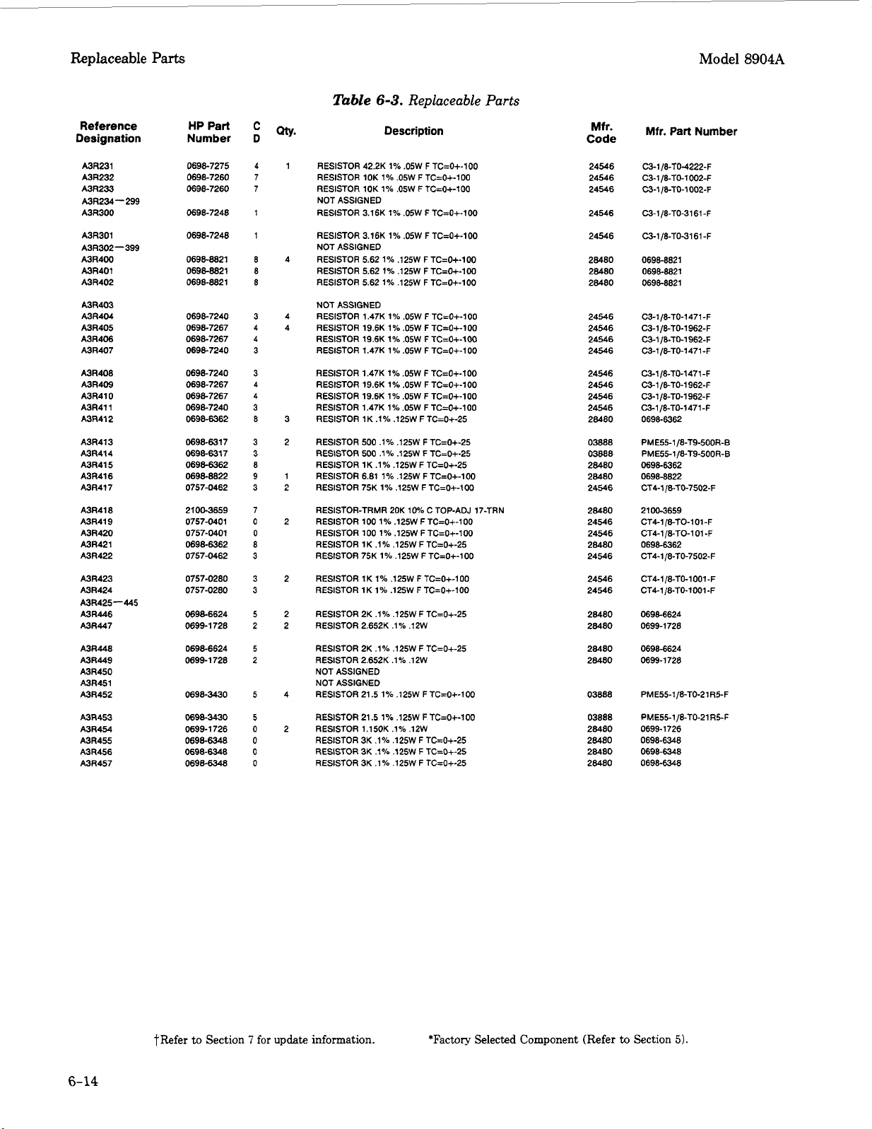
~
~
Replaceable
Reference
Designation
A3R231
A3R232
A3R233
A3R234-299
A3R300
A3R301
A3R302-399
A3R400
A3R401
A3R402
A3R403
A3R404
A3R405
A3R406
A3R407
A3R408
A3R409
0
A3R41
A3R411
A3R412
A3R413
A3R414
A3R415
A3R416
A3R417
A3R418
A3R419
A3R420
A3R421
A3R422
A3R423
A3R424
-445
A3R425
A3R446
A3R447
A3R448
A3R449
A3R450
A3R451
A3R452
A3R453
A3R454
A3R455
A3R456
A3R457
Parts
HP Part
Number
069a7275
069a7260
0698-7260
0698-7246
0698-7246
069a8821
06988821
0698-8821
069a7240
0698-7267
0698-7267
0698-7240
06987240
0698-7267
069a7267
0698-7240
0698-6362
0698-631 7
owam17
069a-2
069a8822
0757-0462
2100-3659
0757-0401
0757-0401
0698-6362
0757-0462
0757-0280
0757-0280
069a6624
0699-1728
069E6624
0699-1728
0698-3430
0698-3430
0699-1726
0698-6348
0698-6348
0698-6348
3
3
3
9
3
7
0
8
3
3
3
5
2
5
2
5
5
0
0
0
0
C
D
4
7
7
1
1
8
8
8
3
4
4
3
3
4
4
8
8
0
Table
atv.
1
RESISTOR 42.2K 1% .05W F TC=0+-100
RESISTOR 10K 1% .05W
RESISTOR 10K 1% .05W F TC=0+-100
NOT ASSIGNED
RESISTOR 3.16K 1% .05W F TC=O+-100
RESISTOR 3.16K 1% .05W F TC=O+-100
NOT ASSIGNED
4
RESISTOR 5.62 1% ,125W F TC=0+-100
RESISTOR 5.62 1% .125W FTC=O+-lOO
RESISTOR 5.62 1% .125W F TC=0+-100
NOT ASSIGNED
4
RESISTOR 1.47K 1% .05W F TC=0+-100
4
RESISTOR 19.6K 1% .05W FTC=0+-100
RESISTOR 19.6K 1% .05W F TC=0+-100
RESISTOR 1.47K 1% .05W F TC=0+-100
RESISTOR 1.47K 1% .05W F TC=O+-100
RESISTOR 19.6K 1% .05W F TC=0+-100
RESISTOR 19.6K 1% .05W
RESISTOR 1.47K 1% .05W F TC=0+-100
3
RESISTOR 1 K .1% .125W F TC=0+-25
RESISTOR 500.1% .125W F TC=0+-25
2
RESISTOR 500 .1% .125W F TC=0+-25
RESISTOR 1K
1
RESISTOR 6.81 1% .125W F TC=0+-100
2
RESISTOR 75K 1% .125W F TC=O+-100
RESISTOR-TRMR 20K 1Ph C TOP-ADJ 17-TRN
2
RESISTOR 100 1% .125W F TC=O+-100
RESISTOR 100 1% .125W F TC=0+-100
RESISTOR 1K
RESISTOR 75K 1% .125W F TC=0+-100
RESISTOR 1K 1% .125W F TC=O+-100
2
RESISTOR 1K 1% .125W
2
RESISTOR 2K .1% .125W F TC=0+-25
RESISTOR 2.652K .1%
2
RESISTOR 2K .1% .125W F TC=0+-25
RESISTOR 2.652K .1% .12W
NOT ASSIGNED
NOT ASSIGNED
4
RESISTOR 21.5 1% .125W F TC=0+-100
RESISTOR 21.5 1% .125W F TC=0+-100
2
RESISTOR 1.15OK .1% .12W
RESISTOR 3K .1% .125W F TC=0+-25
RESISTOR 3K .1% .125W
RESISTOR 3K .1% .125W F TC=0+-25
6-3.
Replaceable
Description
.lo,
.125W F TC=0+-25
.I%
.125W F TC=O+-25
F
.12W
F
TC=O+-lM)
F
TC=0+-100
TC=O+-lOO
F
TC=0+-25
Parts
Mfr.
Code
24546
24546
24546
24546
24546
28480
28480
28480
24546
24546
24546
24546
24546
24546
24546
24546
28480
03888
03688
28480
28480
24546
28460
24546
24546
28480
24546
24546
24546
28480
28480
28480
28480
03868
03888
28460
28480
28480
28480
Model
Mfr. Part Number
‘23-1 /8-TO-4222-F
C3-1/8-TO-1002-F
W-1
E-TO-1002-F
C3-1/8-TO-316l-F
C3-1/8-TO-3161-F
069a8821
0698-8821
069amzi
C3-1 /8-TO-1 471-F
C3-1/8-TO-1962-F
C3-118-TO-1962-F
C3-1/8-TO-1471 -F
C3-1/8-TO-1471-F
C3-1 /8-TO-l962-F
C3-1/8-T0-1962-F
C3-1/8-TO-1471 -F
0698-6362
PME551/8-T9-500R-B
PME55-1/8-T9-500R-B
0698-6362
0698-8822
CT4-1/8-T0-7502-F
21 00-3659
CT4-1/8-TO-lOl-F
CT4-1/8-TO-lOl-F
06986362
CT4-1/8-TO-7502-F
CT4-1 /&TO-lOOl -F
CT4-1/8-TO-1001-F
06986624
0699-1726
06986624
0699-1 728
PME55-1/8-TO-21 R5-F
PME55-1/8-TO-21 RS-F
0699-1726
0698-6346
0698-6348
0698-6348
8904A
6-14
?Refer
to
Section
7
for
update
information.
*Factory Selected Component (Refer
to
Section
5)
Page 23
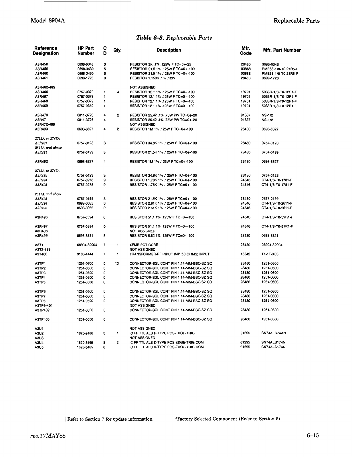
Model
8904A
Table
6-3.
Replaceable
Parts
Replaceable
Parts
Reference
Designation
A3R458
A3R459
A3R460
A3R461
A3R462-465
A3R466
A3R467
A3R466
A3R469
A3R470
A3R471
A3R472-489
A3R490
271ZA
to
2747A
A3R491
and
to
dove
2747A
dove
2817A
A3R491
A3R492
27IZA
A3R493
A3R494
A3R495
2817A and
A3R493
A3R494
A3R495
A3R496
A3R497
A3R498
A3R499
A3T1
A3T2-399
A3T400
A3TP1
A3TP2
A3TP3
A3TP4
A3TP5
A3TP6
A3TP7
A3TP8
A3TP9-401
A3TP402
A3TP403
A3U1
A3U2
A3U3
A3U4
A3U5
HP Part
Number
06984348
069awo
069awo
0699-1726
0757-0379
0757-0379
0757-0379
0757-0379
081 1-3726
081 1-3726
069a8827
0757-0123
0757-0199
06984827
0757-01
23
0757-0276
0757-0278
0757-0199
0698-0085
069a0085
0757-0394
0757-0394
069a882i
08904-80004
9100-4444
1251
-0600
1251 -0600
1251
-0600
1251
-0600
1251-0600
1251
-0600
1251-0600
1251
-0600
1251
-0600
1251-0600
1820-2488
1820-3465
1820-3465
C
D
0
0
0
4
4
4
3
9
9
0
0
0
0
0
0
0
RESISTOR 3K
RESISTOR 21.5
RESISTOR 21.5 1% .125W F TC=0+-100
RESISTOR 1.150K .1% .12W
NOT ASSIGNED
4
RESISTOR 12.1 1% .125W F TC=O+-100
RESISTOR 12.1 1% .125W F TC=O+-100
RESISTOR 12.1 1% .125W
RESISTOR 12.1 1% .125W F TC=0+-100
RESISTOR 25.42 .1% .75W PW TC=0+-20
RESISTOR 25.42 .1% .75W PW TC=O+-20
NOT ASSIGNED
RESISTOR 1M
RESISTOR 34.8K 1% .125W F TC=O+-100
RESISTOR 21.5K
RESISTOR 1M 1% .125W F TC=O+-100
RESISTOR 34.8K 1% .125W F TC=0+-100
RESISTOR 1.78K 1% .125W F TC=O+-100
RESISTOR 1.78K
RESISTOR 21.5K
RESISTOR 2.61K 1% .125W FTC=O+-100
RESISTOR 2.61K 1% .125W F TC=O+-lOO
RESISTOR 51
RESISTOR 51.1 1% .125W F TC=O+-lOO
NOT ASSIGNED
RESISTOR 5.62 1% .125W F TC=0+-100
XFMR POT CORE
1
NOT ASSIGNED
TRANSFORMER-RF INPUT IMP.:50
1
CONNECTOR-SGL CONT PIN 1.14-MM-BSC-SZ
10
CONNECTOR-SGL CONT PIN 1.14-MM-BSC-SZ
CONNECTOR-SGL CONT PIN 1.14-MM-BSC-SZ
CONNECTOR-SGL CONT PIN 1 .lCMM-BSC-SZ
CONNECTOR-SGL CONT PIN
CONNECTOR-SGL CONT PIN 1.14-MM-BSCSZ
CONNECTOR-SGL CONT PIN 1.14-MM-BSCSZ
CONNECTOR-SGL CONT PIN 1 .lCMM-BSC-SZ
NOT ASSIGNED
CONNECTOR-SGL CONT PIN 1.14-MM-BSC-SZ
CONNECTOR-SGL CONT PIN 1.1CMM-BSC-SZ
NOT ASSIGNED
1
IC FF lTL ALS D-PIPE POS-EDGE-TRIG
NOT ASSIGNED
2
IC FF TTL ALS D-PIPE POS-EDGE-TRIG COM
IC FF
.lob
.125W F TC=O+-25
1%
.125W F TC=0+-100
F
1%
.125W F TC=O+-lW
1%
.125W F TC=O+-lOO
1%
.125W F TC=O+-lOO
1%
.125W FTC=O+-100
,l
1% .125W F TC=0+-100
lTL
ALS D-TYPE POS-EDGE-TRIG
TC=O+-100
OHMS;
1
.lQMM-BSCSZ
COM
INPUT
SQ
SQ
SQ
SQ
SQ
SO
SQ
SQ
SO
SO
Mfr.
Code
28480
03888
03888
28480
19701
19701
19701
19701
91637
91 637
28480
28480
28480
28480
28480
24546
24546
28480
24546
24546
24546
24546
28480
28480
15542
28480
28480
28480
28480
28480
28480
28480
28480
28480
28480
01 295
01 295
01295
Mfr. Part Number Description
06986348
PME55-1/8-TO-21 R5-F
PME55-1 /&TO-21 R5-F
0699-1 726
50337-1 /8-TO-l2Rl -F
5WR-1 IaTO-1 2R1 -F
5O33R-1 /ETO-l2Rl -F
5033R-1 /BTO-l 2R1-F
NS-1/2
NS-1/2
069a8827
0757-01
23
0757-01 99
069am27
0757-0123
CT4-1/ETO-1781 -F
CT4-1/&TO-1781-F
0757-0199
c~4-i/a~o26i 1-F
CT~-1
/a~om
1
-F
CTCl/ETO-51Rl-F
CT4-1/8-T0-51 R1-F
mgawi
08904-80004
T1-1T-X65
1251-0600
1251
-0600
1251-OW0
1251-OW0
-0600
1251
1251
-0600
1251-0600
1251-0600
1251-0600
1251
-0600
SN74ALS74AN
SN74ALS174N
SN74ALS174N
rev.17MAY88
?Refer
to
Section 7 for
update
information.
"Factory Selected Component (Refer
to
Section
5).
6-15
Page 24
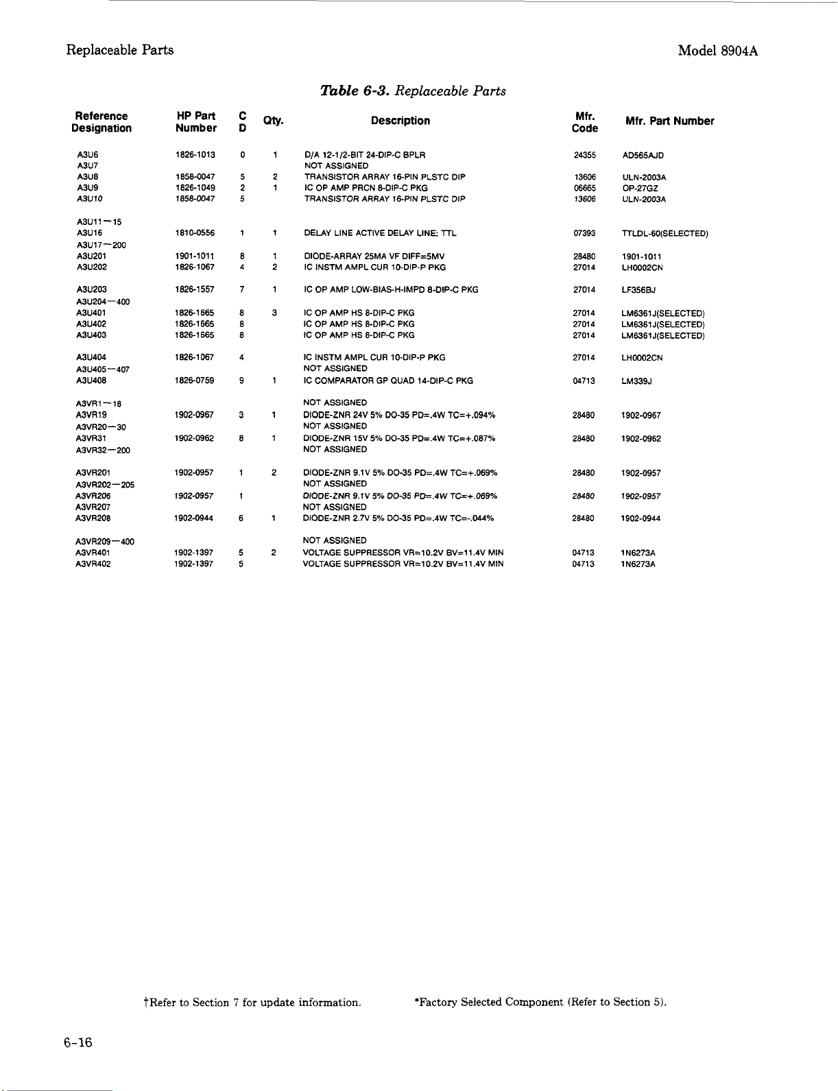
Replaceable
Parts
Model
8904A
Reference
Designation
A3U6
A3U7
A3U8
A3U9
A3U 10
A3U11- 15
A3U16
A3U17-200
A3U201
A3U202
A3U203
A3U204-400
A3U401
A3U402
A3U403
A3U404
A3U405
-
407
A3U408
A3VR1-18
A3VR19
A3VR20-30
A3VR31
A3VR32 - 200
A3VR201
A3VR202
-
A3VR206
A3VR207
A3VR208
A3VR209-400
A3VR401
A3VR402
205
HP Part
Number
1826-1013
1858-0047
1826-1 049
18550047
181 0-0556 1
1901-101
1826-1 067
1826-1
1826-1 665
1826-1665
1826-1 665
1826-1 067
1826-0759
1902-0967
1902-0962
1902-0957 1 2
1902-0957
1902-0944
1902-1397
1902-1 397
557
C
D
0
5
2
5
1
9
3
8
1
6
5
5
Table
6-3.
Replaceable
Description
1
D/A 12-1/2-BIT 24-DIP-C BPLR
NOT ASSIGNED
2
TRANSISTOR ARRAY 16-PIN PLSTC DIP
1
IC OP AMP PRCN 8-DIP-C PKG
TRANSISTOR
1
DELAY LINE ACTIVE DELAY LINE lTL
1
DIODE-ARRAY 25MA VF DIFF=BMV
2
IC INSTM AMPL CUR 10-DIP-P PKG
1
IC OP AMP LOW-BIAS-H-IMPD 8-DIP4 PKG
3
IC OP AMP HS 8-DIP-C PKG
IC OP AMP HS &DIP-C PKG
IC OP AMP HS &DIP-C PKG
IC INSTM AMPL CUR 10-DIP-P PKG
NOT ASSIGNED
1
IC COMPARATOR GP QUAD 14-DIP-C PKG
NOT ASSIGNED
DIODE-ZNR 24V
NOT ASSIGNED
DIODE-ZNR 15V
NOT ASSIGNED
DIODE-ZNR 9.1V
NOT ASSIGNED
DIODE-ZNR 9.1V
NOT ASSIGNED
DIODE-ZNR 2.7V
NOT ASSIGNED
VOLTAGE SUPPRESSOR VR=lO.ZV BV=11.4V MIN
VOLTAGE SUPPRESSOR VR=10.2V BV=l1.4V MIN
ARRAY
16-p~~ PLsrc
5%
DO-35 PD=.4W TC=+.094%
5%
DO-35 PD=.4W TC=+.087%
5%
DO-35 PD=.4W TC=+.069%
5%
00-35 PD=.IW TC=+.O69%
5%
00-35 PD=.4W TC=-.044%
DIP
Parts
Mfr.
Code
24355
13606
06665
13606
07393
28480
27014
27014
27014
27014
27014
27014
04713
28480
28480
28480
28480
28480
04713
0471 3
Mfr. Part Number
AD565AJD
ULN-2003A
OP-27GZ
ULN-2003A
lTLDL-GO(SELECTED)
1901-1011
LH0002CN
LF356BJ
LM6361 J(SELECTED)
LM6361 J(SELECTED)
LM6361 J(SELECTED)
LH0002CN
LM339J
1902-0967
1902-0962
1902-0957
1902-0957
1902-0944
1
N6273A
1N6273A
6-16
tRefer to Section
7
for
update information.
*Factory Selected Component (Refer to Section
5).
Page 25
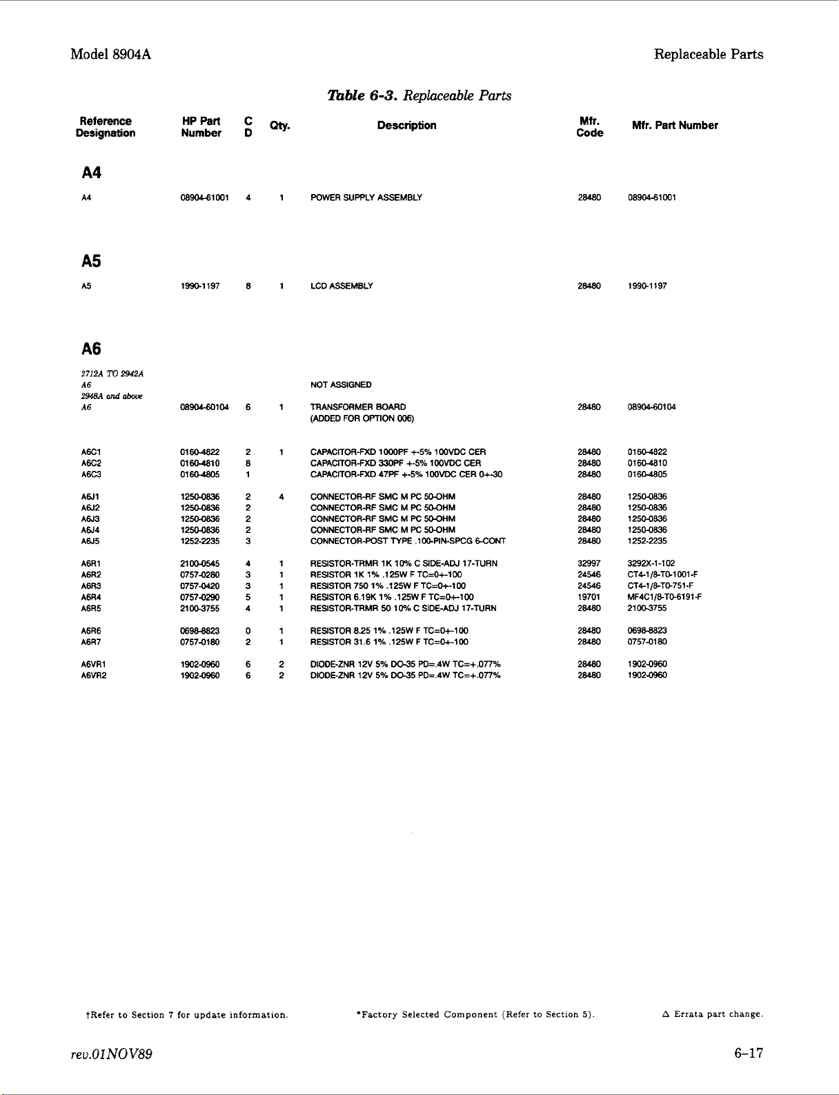
Model
8904A
Replaceable Parts
Reference
Designation Number
HPPart C Description
A4
A4
08904-61001 4 1 POWERSUPPLYASSEMBLY
A5
A5
1-1197 8
A6
271211
To
2942A
A6
2948A
und
above
A6
A6C1
A6C2
A6C3
A6J1
A612
A6J3
AW4
A6J5
A6R1
A6R2
A6R3
A6R4
A6R5
A6R6
A6R7
A6VRl
A6VR2
0890460104 6 1 TRANSFORMERBOARD
01604822
01604810 8 CAPACITOR-FXD 33OPF +-5% 1 00VDC CER
01-5 1 CAPACITOR-FXD 47PF +-5% 1 00VDC CER
12500836
12500836
12500836
12500836
1252-2235
21ooo545 4 1
07574280
07574420
07570290 5 1
21W755 4 1
06988823
07570180
19024960
19024960
nble
6-3.
Replaceable
D
1
LCDASSEMBLY
NOT ASSIGNED
(ADDED
FOR OPTION
2
1 CAPACITOR-FXD 1OOOPF +-5% l00VDC CER
2
2
2
2
3
3 1 RESISTOR 1K 1% .125W F TC=0+-100
3
0
2
6 2 DIODE-ZNR 12V
6
CONNECTOR-RFSMCMPCSOOHM
4
CONNECTOR-RF SMC
CONNECTOR-RF
CONNECTOR-RF SMC
CONNECTORPOST TYPE
RESISTOR-TRMR 1K 10% C SIDE-ADJ 17-TURN
1
RESISTOR 750 1% .125W F TC=O+-lW
RESISTOR 6.19K 1% .125W F TC=Ot100
RESISTOR-TRMR 50 10% C SIDE-ADJ 17-TURN
1
RESISTOR 8.25 1% .125W F TC=O+-lW
1 RESISTOR 31.6 1% .125W FTC=O+-100
2
DIODE-ZNR 12V 5% D(135 PD=.4W TC=+.077%
006)
M
PC
SMC M PC
5%
SOOHM
WHM
M
PC
SOOHM
.I
W-PIN-SPCG
DO35 PD=.4W TC=+.O77%
Parts
0+-30
KONT
Mfr.
Code
28480
28480
28480
28480
28480
28480
28480
28480
28480
28480
28480
32997
24546
24546
19701
28480
28480
28480
28480
28480
Mfr. Part Number
08904-61001
1990-1197
08904-60104
01604822
0160-4810
01 60-4805
1250-0836
12500836
1250-0836
125W836
1252-2235
3292X-1-102
CT4-1 /&TO1 001 -F
CT4-1 /&TO751
MF4C1/5T0-6191-F
21 003755
06988823
0757-01
19020960
19024960
-F
80
tRefer
rev.01
to
Section 7 for update information
NOV89
'Factory Selected Component
(Refer
to
Section
5)
A
Errata part change.
6-1
7
Page 26
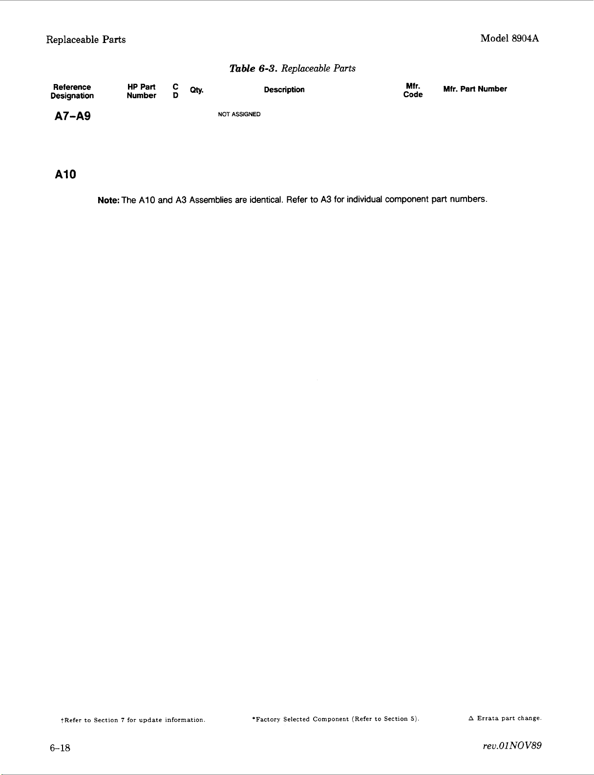
Replaceable Parts
Model
8904A
Reference
Designation Number
HPPart
A7-A9
A10
Note:
The A1 0 and A3 Assemblies are identical. Refer
nble
C Description
D
w’
NOT
ASSIGNED
6-3.
Replaceable
Parts
Mfr-
Code
to
A3 for individual component part numbers.
Mfr.
Part
Number
tRefer to Section 7 for
6-18
update information
*Factory Selected Component (Refer to Section
5)
A
Errata part change.
reu.OlNOV89
Page 27
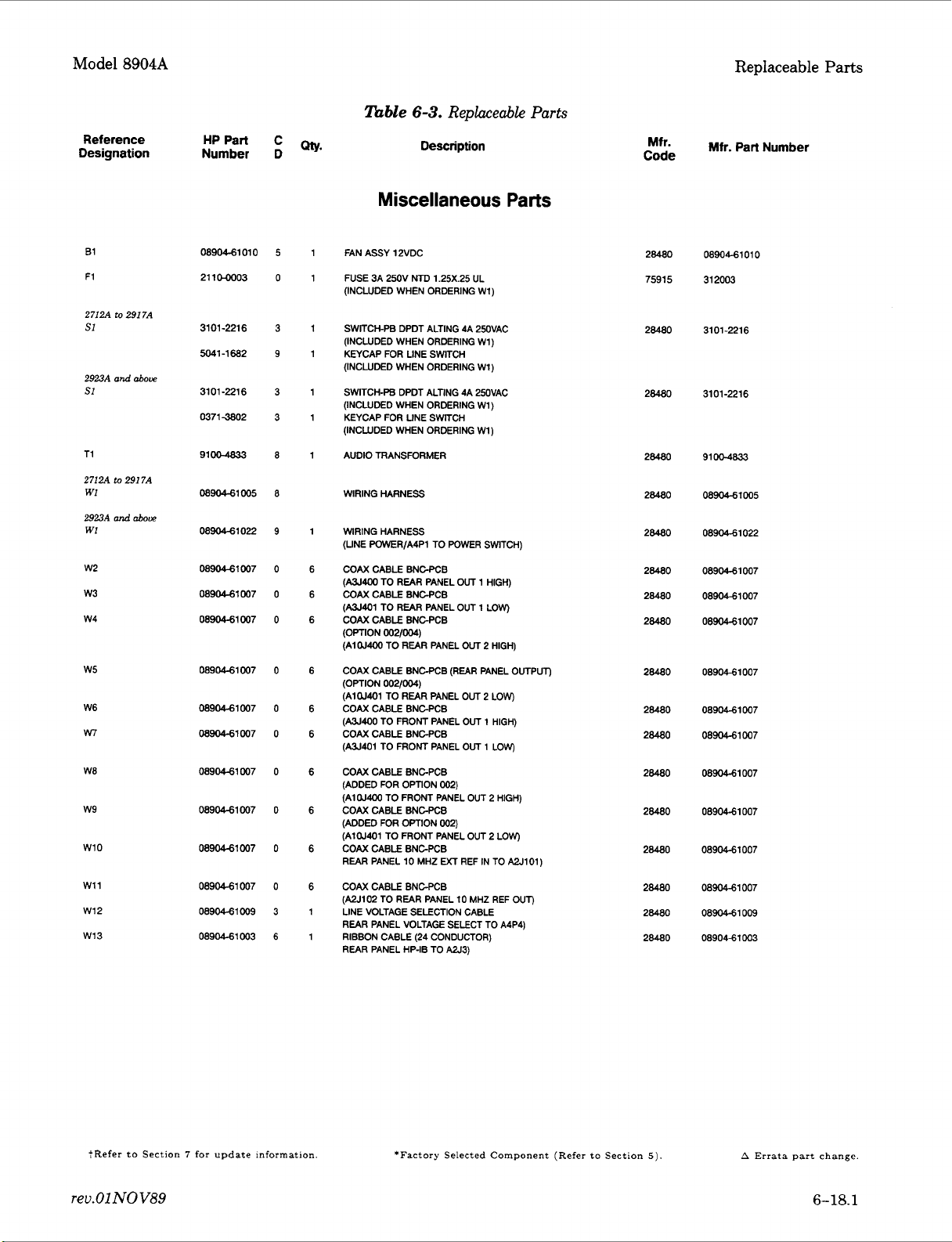
Model
8904A
Reference HPPart
Design at
i
o
n Number
C
D
atv.
%ble
6-3.
Replaceable
Description
Miscellaneous Parts
Parts
Mfr.
Code
Replaceable
Mfr. Part Number
Parts
B1
F1
2712A
SI
2923A
SI
T1
2712A
Wl
2923A
WI
w2
w3
w4
w5
W6
w7
W8
w9
w10
w11
w12
W13
to
and
to
and
2917A
hue
2917A
&ow
08904-61010
21 104003
3101-2216
5041-1682
3101-2216
0371-3602
9100-4833
08904-61005
08904-61022 9
08904-61007
08904-61007
08904-61007
08904-61 007
08904-61007
08904-61007 0 6
08904-61007
08904-61007 0 6 COAXCABLEBNCPCB
089C4-61007
08904-61007 0 6
08904-61 009
08904-61
5
1
FANASSY 12VDC
0
1 FUSE 3A 250V NTD 1.25X.25 UL
(INCLUDED WHEN ORDERING W1)
3
1
SWITCH-PB DPDT ALTING 4A 25OVAC
9
3
3
8
8
0
0
0
0
0
0
0
3
003
6 1 RIBBON CABLE (24 CONDUCTOR)
(INCLUDED WHEN ORDERING W1)
1
KEYCAP FOR LINE SWITCH
(INCLUDED WHEN ORDERING W1)
1 SWITCH-FB DPDT ALTING 4A 25OVAC
(INCLUDED WHEN ORDERING W1)
1
KEYCAP FOR LINE SWITCH
(INCLUDED WHEN ORDERING Wl)
1
AUDIOTRANSFORMER
WIRING HARNESS
1
WIRING HARNESS
(LINE POWER/A4P1 TO
6
COAXCABLEBNCPCB
(-400
TO
6
COAXCABLEBNCPCB
(-401 TO
6 COAXCABLEBNCPCB
(OPTION 002/004)
(AlOJ400 TO
6 COAX CABLE BNCPCB
(OPTION 002/006)
(A1
6
COAXCABLEBNCPCB
(W400
COAXCABLEBNCPCB
(AU401 TO FRONT PANEL OUT 1 LOW)
6 COAXCABLEBNCPCB
(ADDED FOR OPTION
(A1
(ADDED FOR OPTION
(A1 W401 TO FRONT PANEL
6 COAXCABLEBNCPCB
REAR
COAXCABLEBNCPCB
(A2J102
1
LINE VOLTAGE SELECTION CABLE
REAR
REAR
REAR
REAR
REAR
OJ401
TO
REAR
TO FRONT PANEL OUT 1 HIGH)
05400
TO FRONT PANEL OUT 2
PANEL 10
TO
REAR
PANEL VOLTAGE SELECT TO A4P4)
PANEL HP-IB TO AU31
PANEL
PANEL OUT 1 LOW)
PANEL OUT 2 HIGH)
PANEL
MHZ
PANEL 10 MHZ REF
POWER
SWITCH)
OUT
1
HIGH)
(REAR
PANEL OUTPUT)
OUT
2 LOW)
002)
002)
OUT
2
EXl REF IN TO
HIGH)
LOW)
AUlOl)
OUT)
28480 08904-61010
75915 312003
26480
26480 3101-2216
28480 91004833
28480 0890661005
26480
28480 0890461007
28480 0890441007
28480 08904-61007
28480
28480 0890461007
26480 08904-61007
28480
26480 0890441007
28480 0890441007
28480
26480 0890661009
28480
3101-2216
0890661022
08904-61007
0890461007
0890661007
08904-61003
:Refer
to
Section 7 for update information.
rev.OlNOV89
'Factory Selected Component (Refer
to
Section
5).
A
Errata part change.
6-18.1
Page 28
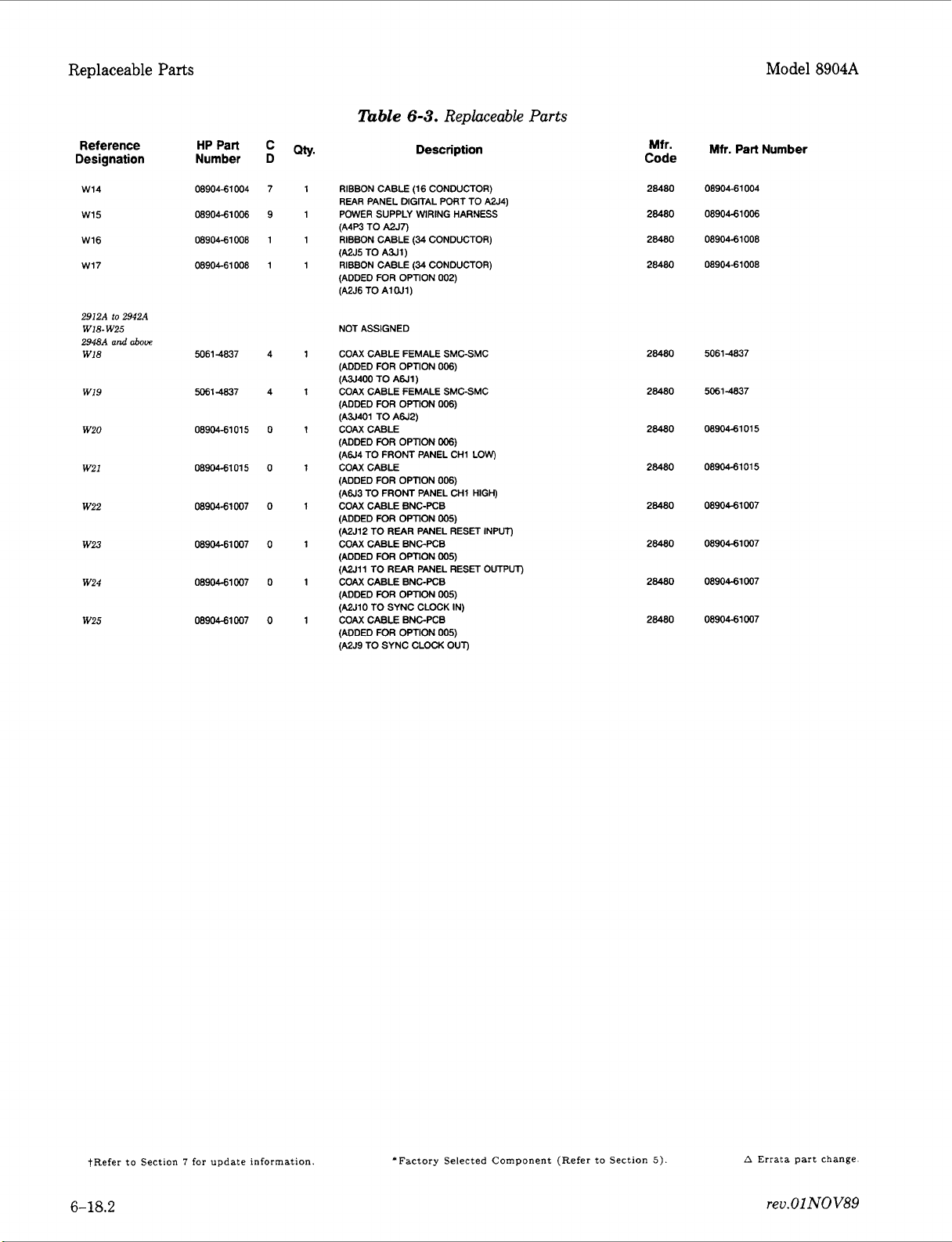
Replaceable Parts
Model
8904A
Reference
Designation
W14
W15
W16
W17
2932A
to
2942A
WI8-
w25
2948A
and
W18
WI9
w20
w21
W22
w23
w24
w25
&ow
HPPart
Number D
0890461004 7
0890461006 9
0890461008 1
08904-61008 1
50614837 4
5061-4837 4
08904-61015 0
08904-61015 0
08904-61007
08904-61007
08904-61007 0
0890461007
C
0
0
0
%ble
QW
1
RIBBON CABLE
REAR
1
POWER SUPPLY WIRING HARNESS
(A4F3 TO A2J7)
1
RIBBON CABLE
(A2J5 TO A3J1)
1
RIBBON CABLE
(ADDED
(A2J6 TO AlW1)
NOT ASSIGNED
1
COAX CABLE FEMALE SMCSMC
(ADDED FOR OPTION 006)
(A3400 TO A6J1)
1
COAX CABLE FEMALE SMCSMC
(ADDED FOR OPTION
(A3401 TO
1
COAX CABLE
(ADDED FOR OPTION
(A6J4 TO FRONT PANEL CH1 LOW)
1
COAX CABLE
(ADDED FOR OPTION
(A6J3 TO FRONT PANEL CH1 HIGH)
COAX CABLE BNC-PCB
1
(ADDED FOR OPTION 005)
(A2J12
1
COAX CABLE BNCPCB
(ADDED FOR OPTION 005)
(AU11 TO REAR PANEL RESET OUTPUT)
1
COAX CABLE BNC-PCB
(ADDED FOR OPTION 005)
(A2JlO TO SYNC CLOCK IN)
1
COAX CABLE BNGPCB
(ADDED
(A2J9 TO SYNC CLOCK
6-3.
Description
(16
PANEL DIGITAL PORT TO A2J4)
(34
(34
FOR
OPTION
A6J2)
TO
REAR
PANEL RESET INPUT)
FOR
OPTION 005)
Replaceable
CONDUCTOR)
CONDUCTOR)
CONDUCTOR)
002)
006)
00s)
006)
OUT)
Parts
Mfr. Mfr. Part Number
Code
28480 0890461004
28480 08904-61 006
28480 0890461008
28480
28480 5061-4837
0890461 008
28480 5061437
28480
28480 08904-61015
28480
28480 0890461007
28480
28480
0890461015
0890461007
08904-61W7
0890661 007
+Refer to Section 7 for update information.
6-18.2
'Factory Selected Component (Refer to Section
5)
A
Errata part change
reu.OlNOV89
Page 29
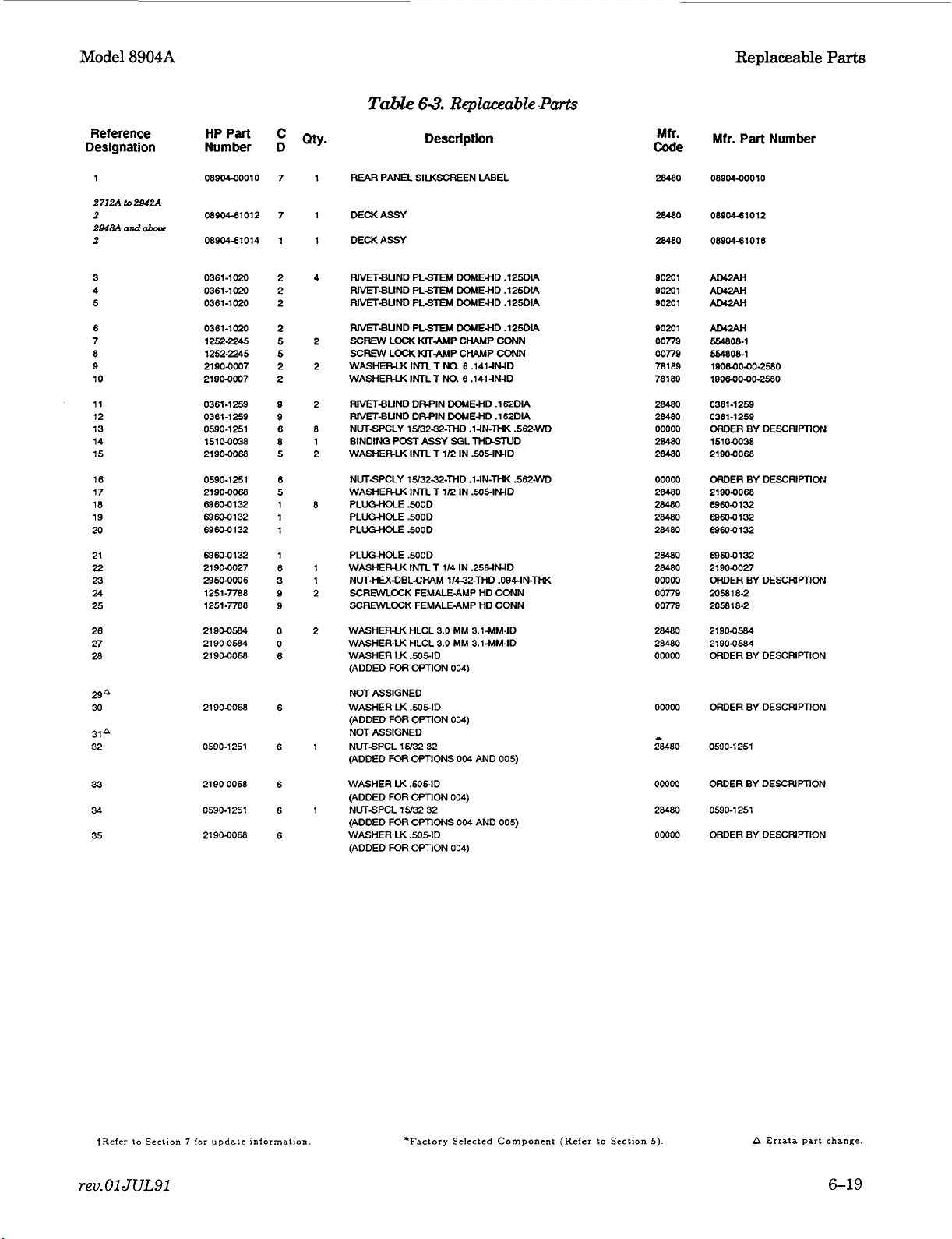
Model
8904A
Replaceable
Parts
Reference
Designation
1
2712A
lo
2u42.4
2
2H8A
and
2
3
4
5
6
7
8
9
10
11
12
13
14
15
16
17
18
10
20
21
22
23
24
25
26
27
28
29A
30
31*
32
33
34
35
abe
HPPart
Number
0890440010
08904-61012 7 1
08904-61014 1 1
0361-1020 2 4
0361-1020 2
0361-1020 2
0361-1020 2
1252-2245 5 2
1252-2245 5
21904007 2 2
21000007 2
0361-1259
03811259 9
0590-1251 6
15104038
21904068 5 2
0590-1251
21904068
69604132 1
69604132 1
69604132 1
69604132 1
21904027
29504006 3 1
i25i-n88
1251-7788
21904584
21904584
21904068 6
21904068 6
0590-1251 6 1
21904068
0590-1251 6 1
21904068 6
Qty.
D
7 1
9
8
6
5
6
9
9
0
0
6
Table
63.
Replaceable
Description
Ru\R
PANEL SILKSCREEN LABEL
DECK ASSY
DECK ASSY
RNFTSUND PLSTEM DOME-HD .125DIA
RIVET-BUND PL-STEM DOME-HD .125DIA
RIVET-BUND PLSTEM DOMEHD .125DIA
RNEF-BUND PLSTEM DOMEHD .125DIA
SCW
LOCK
SCREW
WASHERLK INTLT
WASHEW INnT
2
RNETBUND DWlN
RNET-BUND DRPlN
NLJTSPCLY ly3232-THD
8
BINDING POST ASSY SGL
1
WASHERLK INTLT 1/2 IN
NLJTSPCLY lm232-THD
WASHEW
8
PLUGHOLE
PLUGHOLE
PLUGHOLE
PLUGHOLE
WASHEU INTLT 114 IN 9561KID
1
NLJTHEX-DBL-CHAM 11432-THD
SCREWLOW FEMALE-AMP HD CO"
2
SCREWLOCK
WASHERU HLCL 3.0
2
WASHER-LK HLCL 3.0 MM 3.1-MM-ID
WASHER
(ADDED
NOT ASSIGNED
WASHER
(ADDED FOR OPTION
NOT ASSIGNED
NIJTSPCL 1m2 32
(ADDED
WASHER
(ADDED FOR OPTION
NLJTSPCL 15/32 32
(ADDED
WASHER
(ADDED
KITMP
LOCK WMP CHAMP CO"
NO.
NO.
DOMEHD
DOMEHD
INTL
T 112 IN
.500D
.500D
.50OD
.500D
FEMALE-AMP HD CONN
MM
LK
.505-ID
FOR
OPTION
004)
LK
,505-ID
004)
FOR
OPTIONS
LK
.505-ID
004)
FOR
OPTIONS 004 AND 005)
LK
.5051D
FOR
OPTION 004)
CHAMP CO"
6.1414N-D
6.141-IN-D
.162DIA
.162DIA
.l-IN-THK
.562-WD
THDSFUD
.5051KID
.l-IN-TW
.562-WD
.5051N-ID
.094-IN-T%
3.1-MM-ID
004
AND 005)
.Parts
'". Mfr.
Code
28480
28480 08004-61012
28480 08904-61016
00201
90201
00201
00201
00779 664806-1
00779
78180 19064040-2580
78189 19064040-2580
28480 03614250
28480 0361-1259
00000
28480 15104038
28480 21904068
00000
28480 21004068
28480 69604132
28480 69604132
28480 69604132
28480 69604132
28480 21'904027
00000
oon9
00779
28480 21004584
28480 21904584
00000 ORDER BY
00000
c
28480 0590-1251
00000
28480 0590-1251
00000
Part
Number
080c440010
Awm
m2AH
Aw2AH
mm
664808-1
ORDER BY DESCRIPTION
ORDER BY DESCRIPTION
ORDER BY DESCRIPTION
205818-2
205818-2
DESCWPTION
ORDER BY DESCRIPTION
ORDER BY DESCRIPTION
ORDER
BY DESCRIPTION
rev.
tRefer
to Section 7 for
01
JUL91
update information.
'Factory Selected Component
(Refer
to
Section
5)
A
Errata part change.
6-19
Page 30
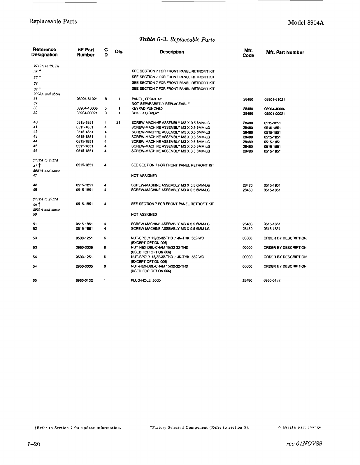
Replaceable
Parts
Model
8904A
Reference
Designation
2712A
to
2917A
36
t
37
t
38
t
39 t
2923A and
36
37
38
39
40
41
42
43
44
45
46
2712A
471
2923A
47
48
49
2712A
50
2923A
50
51
52
53
53
54
54
55 69600132
abow
to
2917A
and
abow
to
291 7A
t
and
abow
HP
Part
Number
0890461021
08904-40006
08904-00021
05151851
05151851
0515-1851
05151851
05151851
051 51 851
0515-1851
05151651
05151851
051 51851
0515-1851 4
051 5-1 851
051.51851
0590-1251
29500035
0590-1251
29500035
C
w.
D
8
1 PANEL, FRONT AY
5
1 KEYPAD PUNCHED
0
1 SHIELD DISPLAY
4
21
4
4
4
4
4
4
4
4
4
8
6
8
1
able
6-3.
Replaceable Parts
Description
SEE SECTION 7 FOR
SEE SECTION
SEE SECTION
SEE SECTION
NOT SEPARARETLY REPLACEABLE
SCREW-MACHINE ASSEMBLY M3 X
SCREW-MACHINE ASSEMBLY M3 X 0.5 6MM-LG
SCREW-MACHINE ASSEMBLY M3
SCREW-MACHINE ASSEMBLY M3 X 0.5 6MM-LG
SCREW-MACHINE ASSEMBLY
SCREW-MACHINE ASSEMBLY M3 X 0.5 6MM-LG
SCREW-MACHINE ASSEMBLY M3 X
SEE SECTION 7 FOR FRONT PANEL RETROFIT KIT
NOT ASSIGNED
SCREW-MACHINE ASSEMBLY M3
SCREW-MACHINE ASSEMBLY M3 X
SEE SECTION 7 FOR FRONT PANEL RETROFIT KIT
NOT ASSIGNED
SCREW-MACHINE ASSEMBLY M3 X 0.5 6MM-LG
SCREW-MACHINE ASSEMBLY M3 X
NUT-SPCLY 15/3232-THD .I-IN-THK ,562-WD
(EXCEPT OPTION
NUT-HEX-DBLGHAM 15/32-32-THD
(USED FOR OPTION
NUT-SPCLY 15/32-32-THD .l-IN-THK ,562-WD
(EXCEPT OPTION
NUT-HEX-DBLGHAM 15/32-32-THD
(USED FOR OPTION
PLUGHOLE .500D
FRONT
7
FOR FRONT PANEL RETROFIT KIT
7
FOR FRONT PANEL RETROFIT KIT
7
FOR FROM PANEL RETROFIT KIT
006)
006)
PANEL RETROFIT KIT
006)
M3
X
X
X
0.5
6MM-LG
0.5
6MM-LG
0.5
6MM-LG
0.5
6MM-LG
0.5 6MM-LG
0.5
6MM-LG
0.5
6MM-LG
006)
Mfr-
Code
28480
28480
28480 08904MM21
28480 05151851
28480 05151851
28480
28480 05151851
28480
28480
28480
Mfr.
Part
08904-61021
0890640006
05151851
05151851
05151851
05151851
28480 05151851
28480 0515-1851
28480 05151851
28480
OMWX)
00000
00000
00000
28480
0515-1851
ORDER BY DESCRIPTION
ORDER BY DESCRIPTION
ORDER BY DESCRIPTION
ORDER BY DESCRIPTION
696041 32
Number
tRefer
6-20
to
Section
7
for
update information.
*Factory Selected Component (Refer
to
Section
5).
A
Errata part change.
rev.01
NO
V89
Page 31

Model
8904A
Replaceable
Parts
Reference
Designation
66
57'5
68A
69
59
60
60
61
62
63
64
65
68
67
68
69
70
71
72
2712A
to
291 7A
73t
74t
2923A
and abm
73
74
75
76
77
78
79
80
81
2712A to2917A
82
83
2923A
and
82
83
abow
HPPart
Number D
69604132 1
29504035
29500035
0590-1251
29500035
50014539
50014539
50414801
50414801
50418801
50418801
50418803
5180-1871 2
0890440016
0890440017
1460-1345
1460-1345 5
05150367
05150367 5
05151234 7
05151234 7
05151234 7
05151234 7
05151234
05151234 7
05151234
05151234 7
0515-1234 7
4
5
7
7
C
8
8
8
8
e
e
8
8
8
8
0
3
5
Table
QW.
PLUGHOLE SOD
NOT ASSIGNED
NOT ASSIGNED
NWHM-DBLCHAM
(USED
FOR
NWHEX-DBLCHAM
(USED
FOR
NWSPCLY
(USED
FOR
NWHMDBLCHAM
(USED FOR
TRIM
2
4
1
1
1
2
2
10
SIDE
TRlM
SIDE
FOOT
NU-lRMOD
FOOT
NU-1RMOD
FOOT
NU-1RMOD
FOOT
NU-1RMOD
TRIM
STRIP (SEE SECTION
LBL
BLK
COVER TOP (SEE SECTION
COVER
TILT STAND SST
TILT STAND
SCREW-MACHINE ASSEMBLY
SEE
SECTION
SCREW-MACHINE ASSEMBLY
SEE SECTION
NOT ASSIGNED
NOT ASSIGNED
SCREW-MACH
SCREW-MACH
SCREW-MACH
SCREW-MACH
SCREW-MACH
SCREW-MACH
SCREW-MACH
SCREW-MACH
SCREW-MACH
NOT ASSIGNED, SEE
NOT ASSIGNED
63.
Replaceable
Description
l5B232-THD
OPTION
002)
l5B232-THD
OPTION
006)
ly32-32-THD .l-IN-THK .562-WD
OPTION
002)
1SD232-THD
OPTION
006)
FRT
F
(SEE SECTION
FRT
F
(SEE SECTION
(SEE SECTION
(SEE SECTION
(SEE SECTION
(SEE SECTION
7)
SERIAL
BOrrOM
SST
7
7
M3.5 X 0.6
M3.5 X 0.6
M3.5 X 0.6
M3.5 X 0.6
M3.5
M3.5 X 0.6
M3.5 X 0.6
M3.5 X 0.6
M3.5 X 0.6
(SEE
FOR
FOR
SECTION
FRONT
FRONT
X
0.6
rEM
7)
M2.5 X 0.45
PANEL
M2.5 X 0.45
PANEL
8MM-LG
8MM-LG
8MM-LQ
8MM-LG
8MM-LG
8MM-LG
8MM-LG
8MM-LG
8MM-LG
145
7)
7)
7)
7)
7)
7)
7)
mom
RETROFIT
Parts
KIT
KIT
Mfr.
Code
28480 69604132
00000
00000
00000
00000
28480
28480
28480
28480
28480
28480
28480
28480
28480
28480
28480
28480
00000
00000
28480 05151234
2UO 05151234
28480 05151234
28480 05151234
28480 05151234
28480 0515-1234
28480 05151234
28480 0515-1234
28480 0515-1234
Mfr.
ORDER
ORDER
ORDER
ORDER
€4014539
50010539
50418801
50414801
50418801
50414801
50414803
5180-1871
0890440016
08904.00017
1460-1345
1460-1345
ORDER
ORDER
Part
Number
BY
DESCRIPTION
BY
DESCRIPTION
BY DESCRIPTION
BY
DESCRIPTION
BY
DESCRIPTION
BY
DESCRIPTION
tRefer to Section 7 for update information.
rev.
01
JUL91
*Factory Selected Component (Refer to Section
5)
A
Errata part changc.
6-2
1
Page 32

Replaceable
Parts
Model
8904A
Reference
Designation
84
85
86
87
88
89
90
91
92
93
94
95
96
97
98
99
100
101
102
103
104
105
106
107
108
109
110
111
112
113
114
115
116
117
118
119
HP
Part
Number
051 51
234
0361 -1 265
0361-1 265
0361-1265
0361-1265
5021-8415
0515-1860
051 51 860
0515-1860
0515-1860
051 51 860
14000249
14000249
14000249
1
W249
14000249
14000249
14000249
14W249
05151851
0515-1851
05151851
05151851
05151851
05151851
05151851
05151851
08904-61013
2190-0585
0515-0955
0380-1914
0380-1 91 4
0380-1 91 4
0380-1914
0380-1 91 4
0380-1914
C
4
4
4
4
4
4
4
4
8
1
7
3
3
3
3
3
3
D
7
7
7
7
7
9
5
5
5
5
5
0
0
0
0
0
0
0
0
Table
Qty.
SCREW-MACH M3.5 X 0.6 8MM-LG
4
RIVET-BLIND PL-STEM DOME-HD .125DIA
RIVET-BUND PLSTEM DOME-HD .125DIA
RIVET-BLIND PL-STEM DOME-HD ,125DIA
RIVETBLIND PLSTEM DOME-HD 325DIA
1
FRAME, FRONT
6
SCREW-MACHINE ASSEMBLY M3.5 X 0.6
SCREW-MACHINE ASSEMBLY M3.5
SCREW-MACHINE ASSEMBLY M3.5
SCREW-MACHINE ASSEMBLY M3.5
SCREW-MACHINE ASSEMBLY M3.5 X 0.6
7
CABLE TIE .062-.625DIA .091-WD NYL
CABLE TIE .062-.625DIA .091-WD NYL
CABLE TIE .062-.625-DIA ,091-WD NYL
CABLE TIE .062-.625DIA ,091-WD NYL
CABLE TIE .062-.625DIA .091-WD NYL
1
CABLE TIE .062D .09W
(ADDED FOR OPTION
1
CABLE TIE .062D .09W
(ADDED FOR OPTION
1
CABLE TIE .062D .09W
(ADDED FOR OPTION
SCREW-MACHINE ASSEMBLY M3
SCREW-MACHINE ASSEMBLY M3
SCREWMACHINE ASSEMBLY M3
SCREWMACHINE ASSEMBLY M3
SCREW-MACHINE ASSEMBLY M3 X 0.5 6MM-LG
SCREW-MACHINE ASSEMBLY M3
SCREW-MACHINE ASSEMBLY
SCREW-MACHINE ASSEMBLY M3
1
AY-SHLD OUT PUT
WASHER-LK HLCL 3.5
1
(ADDED FOR OPTION
1
SCREW-MACH M3.5 X 0.6 30MM-LG PAN-HD
(ADDED FOR OPTION
7
SPACER-RND 19-MM-LG 5.6-MM-ID 10-MM-OD
(ADDED
SPACER-RND 19-MM-LG 5.6-MM-ID 10-MM-OD
(ADDED FOR OPTION
SPACER-RND 19-MM-LG 5.6-MM-ID 10-MM-OD
(ADDED FOR OPTION
SPACER-RND 19-MM-LG 5.6-MM-ID 10-MM-OD
(ADDED FOR OPTION
SPACER-RND 19-MM-LG 5.6-MM-ID 10-MM-OD
(ADDED FOR OPTION 002)
SPACER-RND 19-MM-LG 5.6-MM-ID 1 0-MM-OD
(ADDED FOR OPTION
6-3.
Description
FOR OPTION
Replaceable
004)
004)
004)
MM
3.6-MM-ID
002)
002)
002)
002)
002)
002)
002)
M3
X
X
X
X
X
X
X
Parts
X
0.6
X
0.6
X
0.6
0.5
6MM-LG
0.5 6MM-LG
0.5 6MM-LG
0.5
6MM-LG
0.5 6MM-LG
0.5 6MWLG
0.5
6MM-LG
Mfr.
Code
28480
90201
90201
90201
90201
28480
28480
28480
28480
28480
28480
28480
28480
28480
28480
28480
28480
28480
28480
28480
28480
28480
28480
28480
28480
28460
28480
28480
28480
28480
06540
06540
06540
06540
06540
06540
Mfr.
Part
051 51
234
AD44H
AD44H
AD44H
AD44H
5021-8415
051 5-1
860
051 5-1 860
05151860
0515-1860
051 5-1
860
14000249
14000249
14000249
14000249
14000249
1400-0249
1400-0249
14004249
051 5-1 851
05151851
0515-1851
0515-1851
05151851
05151851
51
851
051
05151851
08904-61 013
2190-0585
051 5-0955
19666N0056
1966GN0056
19666N0056
19666-NW56
19666-NW56
19666-NO056
Number
?Refer to Section 7 for update information
6-22
'Factory Selected Component (Refer to Section
5).
A
Errata part change.
reu.OlNOV89
Page 33

Model
8904A
Replaceable
Parts
Reference
Designation
120
121
122
123
124
125
126
127
128
129
130
131
132
133
134
135
136
137
138
27I2A
to
2817A
I39
2822A
and
139
ubooe
Table
Number
HPPart
0380-1914
0380-1929
14004249
7120-4295 6 1 LABEL-WARNING 1-IN-WD 2-IN-LG AL
14000249 0 1 CABLE TIE .062D .09W
1400-0249
1400-0249 0 1 CABLE TIE .062D .09W
1400-0249 0 1 CABLE TIE .062D .09W
1400-0249
1400-0249
08904-61013 8 1 OUTPUT ASSEMBLY SHIELD
0515-1851 4 1 SCREW 3.0 6 SEM PNTX
05151851 4 1
0515-1851 4 1
05151851 4 1
0515-1851 4 1
0515-1851 4 1 SCREW 3.0 6 SEM PNTX
0515-1851
0515-1851 4 1
08904-00015 2 1 INSULATOR. EPOXY GLASS
3 SPACER-RND 19-MM-LG 5.6MM-ID 1 OMM-OD
0
0
0
0
0
4
(ADDED
1 SPACER-RND 19-MM-LG CMM-ID 3.5MM-THO
(ADDED FOR OPTION
1 CABLE TIE .062D.O9W
(ADDED
(ADDED FOR OPTION 004)
1 CABLETIE .062D .09W
(ADDED
(ADDED FOR OPTION
(ADDED
CABLE TIE .062-.626DIA ,091-WD NYL
1 CABLE TIE .062D .09W
(ADDED FOR OPTION 002)
(ADDED FOR OPTION
(ADDED FOR OPTION
SCREW
(ADDED FOR OPTION 002)
SCREW
(ADDED FOR OPTION 002)
SCREW
(ADDED
SCREW 3.0 6 SEM PNTX
(ADDED FOR OPTION
(ADDED FOR OPTION
1 SCREW 3.0 6 SEM PNTX
(ADDED FOR OPTION
SCREW 3.0 6 SEM PNTX
(ADDED FOR OPTION 002)
NOT ASSIGNED
6-3.
FOR
OPTION 002)
FOR
OPTION
FOR
OPTION
FOR
OPTION
3.0
6 SEM PNTX
3.0
6 SEM PNTX
3.0
6 SEM PNTX
FOR
OPTION 002)
Replaceable
Description
002)
004)
004)
004)
004)
002)
002)
002)
002)
002)
Parts
Mfr.
Code
06540 19666NOO56
06540 1961 6-BoO4O-28
28480 14000249
28480 7120-4295
28480 1400-0249
28480 14000249
28480 14004249
28480 14004249
28480
28480 14000249
28480 0890441013
00000
00000 ORDER BY DESCRIPTION
00000 ORDER BY DESCRIPTION
00000 ORDER BY DESCRIPTION
00000 ORDER BY DESCRIPTION
00000 ORDER BY DESCRIPTION
00000 ORDER BY DESCRIPTION
00000
00000
Mfr.
Part
Number
14000249
ORDER BY DESCRIPTION
ORDER BY DESCRIPTION
ORDER BY DESCRIPTION
tRefer to Section 7 for update information.
reu.OlNOV89
*Factory Selected Component (Refer to Section
5)
A
Errata part change.
6-22.1
Page 34

Replaceable Parts
Model
8904A
lbble
Reference
Designation Number
2712A
to
291 7A
I40
141
and
to
and
to
and
to
and
above
291 7A
aboue
2942A
above
2942A
above
2923A
I40
I41
2912A
142-145
2923A
142
143A 05152028
144A 05150954 6 2 SCREW-MACH M2.5
145 0515-1234
2912A
146-148
2948A
146
147
148
149
2912A
150-166
2948A
150
151
I52
153
154
155
156
157
I58
159
160
I61
I62
I63
164
165
166
HPPart
0890600022
30500891
3050-0891
30500891
08904-8001 5
05151851
05151851
05151860
051
5-1860
05151860
0515-1
860
14000249
14000249
1400249
14000249
14000249
089068001
14000249
08904-0001
E
sty.
1
1
6
2 SCREW-MACH M2.5
7
9 SCREW-MACH M3.5
73
73
73
01
41
41
5
5
5
5
01
01
01
01
01
21
7
01
91
2
NOT ASSIGNED
NOT ASSIGNED
NOT SEPARATELY REPLACEABLE
NOT SEPARATELY REPLACEABLE
NOT ASSIGNED
LINE SWITCH BRACKET
NOT ASSIGNED
WASHER-FL
WASHER-FL MTLC
WASHER-FL
NOT ASSIGNED
NOT ASSIGNED
LABEL
SCREW
(ADDED
SCREW
(ADDED
SCREW-MACHINE ASSEMBLY M3.5
(ADDED
SCREW-MACHINE ASSEMBLY
(ADDED
SCREW-MACHINE ASSEMBLY M3.5
(ADDED
SCREW-MACHINE ASSEMBLY M3.5
(ADDED
CABLE TIE .OED .WW
(ADDED
CABLE TIE
(ADDED FOR OPTION 005)
CABLE TIE .062D .WW
(ADDED FOR OPTION 005)
CABLE TIE
(ADDED FOR OPTION 005)
CABLE TIE
(ADDED FOR OPTION
LABEL FOR OPTION 005
NOT ASSIGNED
NOT SEPARATELY REPLACEABLE
CABLE TIE
(ADDED
BOARD
FOR
OPTION
3.0
6
FOR
3.0
6
FOR
FOR
FOR
FOR
FOR
FOR
.062D .WW
.062D
.062D
.062D .WW
FOR
PULLER
MTLC
MTLC
SEM
OPTION
SEM PNTX
OPTION
OPTION
OPTION
OPTION
OPTION
OPTION 005)
OPTION
6-3.
Replaceable
Description
X
0.45 4MMLG
X
0.45
X
0.6 8MM-LG
3.OMM
3.OMM
3.OMM
006
PNTX
006)
006)
006)
006)
006)
006)
.09W
.WW
005)
006)
4MMLG
3.3MM-ID
3.3MM-ID
3.3MM-ID
M3.5
X
X
X
X
0.6
0.6
0.6
0.6
Parts
Mfrm
Code
28480
28480
28480 05150954
28480
00000
00000
00000
28480
00000
00000
28480
28480
28480
28480
28480
28480
28480
28480
28480
28480
28480
28480
Mfr. Part Number
08904-00022
05150954
05151234
ORDER BY DESCRIPTION
ORDER BY DESCRIPTION
ORDER BY DESCRIPTION
089Od80015
ORDER
ORDER BY DESCRIPTION
051
5-1
8M)
051
51
860
05151860
51
860
051
1400.0249
1400.0249
1400-0249
1400.0249
1400.0249
08900-80017
1400.0249
08904-00012
BY DESCRIPTION
tRefer
6-22.2
to
Section 7 for update information.
*Factory Selected Component (Refer to Section
5)
A
Errata part change.
reu.OlNOV89
Page 35

I'ZZ-9
68AON
1O'naJ
Page 36

Replaceable Parts
Model
8904A
6-22.4
Figure
6-1.
Main
Deck
Assembly
-
Top,
(2923A and
L
.'
above)
rev.
01
NOV89
Page 37

Model
8904A
Replaceable
Parts
rev.30NOV89
Figure
6-1.
Main
Deck
Assembly
-
Top,
Option
005
(2948A
and
above)
6-23
Page 38

Replaceable Parts
Model
8904A
6-24
Figure
6-2.
Main
Deck
Assembly
-
Bottom
reu.3ONOV89
Page 39

Model
8904A
Replaceable
Parts
rev.30NOV89
Figure
6-2.
Main
Deck Assembly
-
Bottom,
Option
006
(2948A
and above)
6-24.1
Page 40

Replaceable
Parts
Model
8904A
/;
W
0
W
W
wl
6-24.2
Figure
6-3.
Front
Panel
Assembly,
(2712A
to
291
7A),
See Section
7
for
Front
Panel
Retrofit Kit.
reu.30NOV89
Page 41

Model
8904A
Replaceable
Parts
reu.30NOV89
Figure
6-3.
Front Panel Assembly,
(2923A
and above)
6-24.3
Page 42

Model
8904A
Replaceable
Parts
reu.30NOV89
Figure
6-3.
Rent
Panel
Assembly,
Option
006
(2948A
and
above)
6-25
Page 43

Replaceable
Parts
Model
8904A
6-26
Figure
6-4.
Rear
Panel
Assembly
rev.
30NO
V89
Page 44

Model
8904A
Replaceable Parts
rev.
30N0
V89
Figure
6-4.
Rear Panel
Assembly,
Option
005
(2948A
and above)
6-26.1
Page 45

Model
8904A
Replaceable Parts
rev.ZSSEP88
Figure
6-5.
Covers,
Labels,
and
ROMs
6-27
Page 46

Replaceable
Parts
Model
8904A
6-28
Figure
6-6.
Output
Cables
(1
of
2)
reu.30NOV89
Page 47

Model
8904A
Replaceable Parts
Q
rev.
30N0
V89
Figure
6-6.
Output Cables, Option
005
(29484
and above)
(2
of
2)
6-29
Page 48

H
P
8 9 0
4
A
Table
of
Contents
TABLE
OF
Section
Instrument Changes
Introduction to This Section
Option Conversions
Instrument Modifications
Front-To-Rear-Panel Output Conversion
Description
Parts Required
Tools Required
Modification Procedure
Operation Verification
Rear-To-Front-Panel Output Conversion
Description
Parts Required
Tools Required
Modification Procedure
Operation Verification
Firmware Updates (A2U12 and A2U13)
Modification For Possible Ground Wire Shock Hazard
Modification
Modification For Potential Power Supply Short
Cabinet
Modification
For
Parts
Color Change
For
.................................................
....................................................
......
..................................................
....................................................
..................................................
..................................................
Output Overvoltage Protection Improvement
Front Panel Assembly
............................................
..............................................
......................................
:
...........................................
.............................................
..............................................
......................................
.............................................
..............................................
......................................
.................................
............................................
.....................................
CONTENTS
7
.............................
........................
7.1
7.1
7.2
7-3
7.3
7.3
7.3
7.3
7-4
7-5
7.5
7.5
7.5
7.5
7.6
7.9
7-10
7-13
7-14
7-14
7-15
Page 49

Model
8904A
Instrument Changes
7-1.
INTRODUCTION TO
This section contains instrument modification recommendations and procedures that could improve
the performance and reliability of your instrument. Refer to
section
number coverage.
7-2.
OPTION CONVERSIONS
It
HP
1
of the HP
is
sometimes desirable to add
8904A
Multifunction Synthesizer this can be done as indicated in the following table.
Number
001
002
003
004
Delete
005
006
004
Section
7
INSTRUMENT CHANGES
THIS
SECTION
8904A
Operation and Calibration Manual
or
delete options in the instrument after the initial purchase. In the
I
2942A
and below
Yes
Yes
Yes
Yes
Yes
No
No
Yes, except in combination with Option
Yes, except in combination with Option
Yes, except in combination with Option
Instruments Covered
for important information about serial
294814
and above
Yes
Yes
Yes
Yes
by
005
This
or
004
004
Manual
006
in
To
capability), order HP
To
Hewlett-Packard Sales office.
To
Hewlett-Packard Sales office.
To retrofit Option
titled
005
To
section titled
To
Hewlett-Packard Sales office. Only instruments with serial prefix
with this option.
rear-panel connectors will need to be moved to the front panel.
rev.15DEC89
retrofit Option
retrofit Option
retrofit Option
001
(three internal channels, channel A modulation, summation, and sequence
11816A
002
003
(fast hop and digital modulation capability), order
004
(front-panel connectors moved to rear panel), follow the instructions in section
from your local Hewlett-Packard Sales office.
(second internal synthesizer and output), order
Front-to-Rear-Panel Output Conversion.
(multi-instrument phase synchronization)
delete Option
004
(rear-panel connectors moved to front panel), follow the instructions in the
Rear-to-Ront-Panel Output Conversion.
retrofit Option
005
(multi-instrument phase synchronization), order
If
the instrument has Option
HP
11817A
HP
11818A
This option cannot be added in combination with Option
or
006
(balance output).
HP
11827A
004
(front-panel connectors
2948A
and above can be retrofit
moved
from your local
from your local
from your local
to
rear panel), the
7-
1
Page 50

Instrument Changes Model
To
retrofit Option
office. Only instruments with serial prefix
006
(balance output), order HP
2948A
11837A
from your local Hewlett-Packard Sales
and above can be retrofit with this option. The
added balanced output will replace one of the outputs already in the instrument if it has Option
(second internal synthesizer and output).
moved to rear panel), the rear-panel connectors will need
7-3.
INSTRUMENT MODIFICATIONS
If
the instrument has Option
to
be moved to the front panel.
004
(front-panel connectors
8904A
002
Instrument modifications include firmware updates and hardware modifications.
firmware updates refer to the following table and to the section titled
Serial Prefix
~
2732A
and
below
2737A
to
2942A
2948A
and above
'Two revisions
the newer revision has part number
of
firmware share the same revision code: 22987A. The older revision has part number HP 08904-87007 for
Revision Code
~
~~
20987A
and
22987A
22987A
27887A
HP 08904-87010.
For
information on
Firmware Updates.
~~
The first
though useable. It is recommended that all instruments be upgraded to
Revision
Problems noted in the previous firmware revision were fixed. However, the
following problem has been noted: When used with HP-IB controllers which
process HP-IB commands very fast, the instrument may hang up the HP-IB
when the instrument is a talker. This problem can
to Revision
Problems noted in the previous firmware revisions were fixed. Programs for
operating Options
to Option
of
retrofitted into older instruments.
two
editions of firmware had several problems and were incomplete,
22987A
with HP
22987A
with HP
005
001:
Hop
RAM
the controller was made which does not permit this added firmware to be
Firmware History
08904-8701
08904-8701
and
006
were added. Two enhancements were added
sequencing and
0
as
A2U12*.
0
as
FM
be
corrected by upgrading
A2U12'.
stereo. A physical re-design
ROM
A2U12;
7-2
For
titled
Serial Prefix
2737A
and below
2747A
and below
281 7A
and below
291 7A
and below
information on recommended hardware modifications refer to the following table and to the section
Hardware Modifications.
Nature of Modification
Modification for possible ground wire shock hazard.
Modification for output overvoltage protection improvement.
Modification for potential power supply short.
Modification for front panel assembly.
rev.
15DEC89
Page 51

Model 8904A Instrument Changes
7-4.
FRONT-TO-REAR-PANEL OUTPUT CONVERSION
Description
This procedure describes how to convert an instrument with front-panel output connectors (that is, a
standard instrument) to one with rear-panel connectors (that is, Option
to instruments with one pair of outputs
or
two
(that is, Option
002).
004).
The procedure applies
The modifications requires partial disassembly of the instrument (removing covers and routing of
No
cables).
soldering
modification,
two
is
required. Modification should be done in a static protected environment. After
performance tests must be run.
Parts Required
The following parts are required and may be ordered by contacting the nearest Hewlett-Packard Sales
Office.
Table
Standard
Option 002
Standard
Option
Option
002
7-1.
Parts
I
Quantity
for
HP
8904A
Plastic
Plastic Hole-Plug
Lock Washer
Lock Washer
Cable
Label
Tools Required
The following tools are needed to modify the instrument:
9/16 inch, 6 point Nut Driver
No.
2
Pozidriv Screwdriver
Diagonal Cutters
Needle-nose Pliers
Modification Procedure
Removing
Bottom
Cover
Rant-to-Rear-Panel
Description
Hole-Plug
0.505
inch
ID
0.505
inch
ID
Tie
Blank
Output
Conversion
HP Part Number
6960-01
6960-01
21
90-0068
21
90-0068
1400-0249
51
80-1 871
32
32
Preparing the Chassis
rev.15DEC89
1.
Turn the instrument
2.
Lay the instrument on its top and unscrew the Pozidriv screw in the middle of the rear edge of
the bottom cover. This
frame. Slide the cover back about 6.5 mm
1.
Remove the nuts from the present front-panel outputs with the 9/16 inch nut driver. Do not
press against the front panel with the tool
2.
Remove the cable tie around the loop of slack coaxial cable in the instrument by cutting it with
off
and unplug the power cord.
is
a captive screw and will cause the bottom cover to push away from the
(0.25
inch) and lift
or
scoring of the panel may occur.
it
off.
the diagonal cutters being careful not to score the soft insulation on the cables.
3.
Remove the necessary plastic hole-plugs in the rear panel by approaching them from inside the
chassis with the needle-nose pliers and squeezing-in the small holding tangs on opposite sides
of the plug. Grasp the front of the plug with your fingers
or
attempt to pry the plug out from the panel
the panel surface may get scarred.
to
pull
it
away from the panel.
Do
Front-to-Rear-Panel Output Conversion
not
7-3
Page 52

Instrument Changes Model 8904A
Cable
Routing
1.
Refer to figures 7-1, 7-2 and 7-3. Remove the BNC connector ends from the front panel one at
a time and insert them into the corresponding openings in the rear panel.
2.
After all of the connectors have been transferred to the rear panel, secure the cables to the side
rail as shown in figure 7-3 using the new cable ties.
3.
Install one new lock washer and one new nut on each connector.
4. Tighten the nuts on the BNC connectors hand tight using the nut driver. (The holes in the panel
are
D
shaped and therefore prevent the connector from turning without having to tighten the
nuts excessively.)
5. Verify that the
Option
Final Steps
1.
Insert the new plastic hole-plugs into the front-panel output openings by carefully working the
plugs into the holes with your fingers. The plugs
them started in the holes.
2.
Replace the bottom cover by reversing the removal procedure.
3.
Type or write the date and option number on the new blank label in the following form:
002,
the A10 Output Assembly are tight.
day/month/year
(Do
panel.
not place the label over the existing serial number tag.)
Operation Verification
1.
Connect the power cord and turn the instrument on.
2.
The instrument should beep immediately upon power up and then again about 4.5 seconds later.
The display should read
3.
Key in the following keys. (This will set up
ground the
LOW
SMC
connections on the
:
Opt
.
*
I
fl
Channel Confie.
connector.)
A3
Output Assembly and,
fit
tightly and will require some pressure to get
004.
Peel
off
the protective backing and stick the label
HP
8904A Main Selection Level
5
V
dc on the
if
the instrument has
*I
OUTPUTS 1 HIGH
on
the rear
connector and
fl
(Channel Conf
NEXT
SHIFT FLOAT
WAVE FORM
AMPTD
4.
Connect a DC voltmeter, set to measure a
The voltmeter should read approximately
5. If the instrument is equipped with a second output, Option 002, key in
NEXT
SHIFT FLOAT
WAVE FORM
AMPTD
6.
Connect the DC voltmeter to the
approximately 5 V dc.
7.
Perform the
the HP 8904A
7-4 Front-to-Rear-Panel Output Conversion
AC and
=
5
V
2
5=1
5
V
DC
Operation and Calibration Manual.)
ig.
1
OFF
OFF
Amplitude Accuracy
)
5
V
5
V
dc.
OUTPUTS 2 HIGH
Test
dc signal, to the
connector. The voltmeter should read
and the
AC Amplitude Flatness Test.
OUTPUTS 1 HIGH
rev. 15DEC89
connector.
(Refer
+,.
Page 53

Model
7-5.
8904A
REAR-TO-FRONT-PANEL OUTPUT CONVERSION
Description
This procedure describes how to convert an instrument with rear-panel output connectors (that is,
Option
to instruments with one pair of outputs
004)
to one with front-panel connectors (that
or
two
is,
a standard instrument). The procedure applies
(that is, Option
Instrument Changes
002).
The modifications requires partial disassembly
cables). No soldering
modification,
two
is
required. Modification should be done in a static protected environment. After
performance tests must be run.
Parts Required
The following parts are required and may
Oflice.
Option Quantity
Option Quantity
Tools
Required
Standard
Standard
Option
002
Option
002
2
2
4
4
3
3
The following tools are needed to modify the instrument:
9/16
inch, 6 point Nut Driver
No.
2
Pozidriv Screwdriver
Diagonal Cutters
Needle-nose Pliers
be
ordered by contacting the nearest Hewlett-Packard Sales
Plastic
Plastic
Plastic
Plastic
Cable
Cable
bf
the instrument (removing covers and routing of
Description HP Part Number
Description HP Part Number
Hole-Plug
Hole-Plug
Hole-Plug
Hole-Plug
Tie
Tie
6960-01 32
6960-01 32
6960-01 32
6960-01 32
1400-0249
1400-0249
Modification Procedure
Removing Bottom Cover
1.
Turn the instrument
2.
Lay the instrument on
the bottom cover. This
frame. Slide the cover back about
Preparing
1.
2.
3.
rev.15DEC89
the
Remove the nuts from the present rear-panel outputs with the
against the rear panel with the tool
Remove the cable ties that secure the coaxial output cables to the sideframe by cutting them
with diagonal cutters being careful not to score the soft insulation on the cables.
Remove the necessary plastic hole-plugs in the front panel by approaching them from inside the
chassis with the needle-nose pliers and squeezing-in the small holding tangs on opposite sides
of the plug. Grasp the front
attempt to pry the plug out from the panel
Chassis
off
and unplug the power cord.
its
top and unscrew the Pozidriv screw in the middle of the rear edge of
is
a captive screw and will cause the bottom cover to push away from the
6.5
mm
(0.25
inch) and lift
or
scoring of the panel may occur.
of
the plug with your fingers to pull it away from the panel.
or
the panel surface may get scarred.
it
off.
9/16
inch nut driver.
Do
Rear-to-F'ront-Panel Output Conversion
not press
Do
not
7-5
Page 54

Instrument Changes Model 8904A
Cable Routing
1.
Refer to figures
a
time and insert them into the corresponding openings in the front panel.
2.
After all of the connectors have been transferred to the front panel, loop the cables and secure
them to the front of the deck using the new cable ties as shown in figure
3.
Install one nut on each connector.
7-1, 7-2
and
7-3.
Remove the BNC connector ends from the rear panel one at
7-3.
4. Tighten the nuts on the BNC connectors hand tight using the nut driver. (The holes in the panel
are D shaped and therefore prevent the connector from turning without having to tighten the
nuts excessively.)
5.
Verify that the SMC connections on the
Option
Final Steps
1.
Insert the new plastic hole-plugs into the rear-panel output openings by carefully working the
002,
the
A10
Output Assembly are tight.
plugs into the holes with your fingers. The plugs
A3
Output Assembly and, if the instrument has
fit
tightly and will require some pressure to get
them started in the holes.
2.
Replace the bottom cover by reversing the removal procedure.
3.
Remove the Option
004
label from the rear panel.
Operation Verification
1.
Connect the power cord and turn the instrument on.
2.
The instrument should beep immediately upon power up and then again about
The display should read
~~
*
HP
8904A
fl
Channel Config.
3.
Key in the following keys. (This will set up
ground the
LOW
fl
(Channel
connector.)
Config.
Main
Selection Level
5
V
dc on the
*
OUTPUTS
NEXT
SHIFT FLOAT 1 OFF
5
5
V
V
r
2
=
OFF
5
V
dc signal, to the
5
V
dc.
002,
OUTPUTS
key in
WAVE FORM
AMPTD
4.
Connect a DC voltmeter, set to measure a
The voltmeter should read approximately
5.
If the instrument is equipped with a second output, Option
NEXT
SHIFT FLOAT
WAVE FORM
AMPTD
1
4.5
HIGH
connector and
1
HIGH
seconds later.
connector.
7-6
6. Connect the DC voltmeter to the
approximately
7.
Perform the
the
HP
8904A
5
V
dc.
AC and DC Amplitude Accuracy Test
Operation and Calibration Manual.)
Rear-to-Front-Panel Output Conversion
OUTPUTS
2
HIGH
and the
connector. The voltmeter should read
AC Amplitude Flatness Test.
(Refer to
reu.15DEC89
Page 55

Model
8904A
Instrument
Changes
Figure
7-1.
Ront Panel Output Hardware
\
h
rev.lSDEC89
Figure
7-2.
Rear Panel Output Hardware
7-7
Page 56

Instrument Changes
Model
8904A
w5
Figure
7
-8
7-3.
Output
Cable
Routing
(ALL
Options)
rev.
15DEC89
Page 57

Model
89048
Instrument Changes
7-6.
FIRMWARE
The -ware
corrected by altering the Controller’s program. Firmware
may
only
Replacing the
Use the following procedure
UPDATES (A2U12 AND A2U13)
is
changed whenever anomalies are found
be
changes
in
the
program, or which may
ROMs
to
install
The
ROMs
tions
(MU12 and MU131 are static sensitive devices. Takeprecau-
against electrostatic discharge
new
ROMs:
nents.
NOTE
In instruments with serial prefix 2942A and below, the finware is stored
in two
and above, the firmware
a different
1.
Unplug the power
ROMs
(MU12 andA2U13). In instruments with serialprefix2948A
is
stored only in
function)
cord.
also
@SD)
one
in
the
instrum
is
also
changed
result
from
before handling these compo-
ROM
(MU12).
ent’s
operation which can
to
add new features, which
instrument hardware changes.
(MU13 serves
be
2. Remove the top cover.
the top cover does not
screw on the rear edge of the bottom cover also.
3.
For
instruments
(front horizontal board). For
in
They are
4.
Pry
out
5.
Plug
in
6.
Check
Serial Prefix 2740A and
The recommended replacement for MU12
for MU13
part number differs.
Serial Prefix 2742A and above:
The recommended replacement for MU12
for MU13
sockets.
the old
the new ROM or
the
is
HP
is
HP
ROM
operation
Part
Part
The
cover may
pull
off
with
serial
prefix 29428 and below, inlocate U12 and U13 onthe
instrum
The
reference designator
or
ROW
ROMs
of
the
instrument.
below:
08904-87008.
08904-87009.
easily after backing out the screw on the rear edge, back out the
with a blade-type screwdriver.
in
the correct sockets and with
If
either MU12
be
tightly secured
ents with
is
HP
Part
is
HP
Part
in
the groove of the bottom cover.
A2
assembly
serial
prefix 2948A and above, locate only U12.
is
labeled beside the IC.
the
correct pin orientation.
08904-87010. The recommended replacement
or
MU13 fails, replace the other part
08904-87011. The recommended replacement
also
if
If
its
rev.
01
JUL91
Firmware UpdatesBardware Modifications
7-9
Page 58

Instrument Changes Model
7-7.
MODIFICATION
FOR
POSSIBLE
GROUND
WIRE
SHOCK HAZARD
8904A
(Serial Prefix
This information explains how to check for the possible shock hazard and how to correct it. The check
for
the shock hazard is by simple visual inspection. Corrective action, if needed, consists
the ground wire with attention paid to wrapping and soldering it
the wire should be made by someone with wire soldering skills.
2737A
On some instruments with serial prefix
wire from
been wrapped and soldered in compliance with strict safety standards.
condition does not create a safety hazard under normal use; however, a safety
hazard can develop
(1)
the connections can erode, weaken, and eventually cause the connections to
loosen. Should ground contact break,
to be at ground potential.
(2)
neutral or high lines of the power cord come in contact with the chassis
through some other fault. The chassis
With
wire will maintain a reasonable mechanical connection even though
has
and
below)
2737A
the
rear-panel line socket to
if
the following
If
the
ground wire ever sustains heavy current long enough,
With ground contact interrupted, the chassis could become “hot” if
proper wrapping and soldering of
deteriorated.
two
the
conditions occur.
the
chassis can no longer be guaranteed
then
the
and below,
metal chassis may not have
becomes a shock hazard.
ground connections,
to
the
grounding
the
solder on
the
ground
the
its solder lugs. Replacement of
This
the
solder
of
replacing
The following parts may be required
1
Description
Cable
Tie
Wire
(Green/Yellow)
I
Quantity
1
HPPart Number
0360-0036
1400-0249
81
50-291
I
9
7-10
Firmware Updates/Hardware Modifications
rev.
15DEC89
Page 59

Model
8904A
Instrument Changes
Checking
1.
2.
3.
4.
5.
6.
for
the Shock
Unplug the power cord from its rear-panel socket.
Remove the instrument’s top cover by backing out the screw in the center of the rear edge of the
cover. This is a captive screw and will cause the cover to push away from the frame.
Refer to figure
is inside the rear panel in the right rear corner of the instrument beneath the red and silver
warning label.
Carefully slit the black shrink tubing over the ground wire connection to the line socket. A sharp
X-acto knife is recommended. (The shrink tubing will not be replaced.)
Inspect the soldered wire connection on both ends of the ground wire and compare the wire
wrapping to figure
the socket ground connection on the rear-panel line socket.
If the solder joints are properly wrapped and soldered, replace the top cover and make a quick
of
check
the operation of the instrument.
Hazard
7-4.
Locate the ground wire.
7-5.
One end of the wire goes
\
It
has green insulation with a yellow stripe and
to
the chassis ground lug and the other end to
/-WARNING LABEL
Figure
7-4.
’
Parts Location (Shown
/\
with
Power
BLACK WIRE
GREENVELLOW GROUND
MAIN HARNESS (GRAY)
Supply
Removed)
WIRE
rev.
15DEC89
Firmware Updates/Hardware Modifications
7-11
Page 60

Instrument Changes Model 8904A
GOOD WRAPPING
Wire is mechanically secure prior to
The
soldering.
three quarters
POOR
(1)
Wire is not mechanically secure prior
to soldering.
(2)
Wrap is less than three quarters turn.
(3)
Wrap
wire wrap is at least
to
one full turn.
WRAPPING
exceeds
one full turn.
~~ ~ ~~
Figure
Replacing
1.
the
Ground
Wire
If the wrap on either end of the ground wire
7-5.
Ground Wire Wrapping
________~
is
not within specification, the ground wire must
be replaced.
or
2. Remove the screw holding the ground wire to the instrument standoff. (Use a T10
T15 Torx
screwdriver as needed.)
3.
Cut the gray cable tie which secures the main wire harness to the standoff with a pair
of
diagonal
wire cutters. Avoid cutting into the insulating sheath of the harness.
4.
With the main harness free, move
5.
Heat the soldering iron. You will also need a roll of solder wick.
it
up and to the left
so
as not to interfere with soldering.
6. On the line cord socket, heat the solder on the lug where the ground wire is attached and apply
the solder wick.
At
the same time move the ground wire around and pull the ground wire out
the lug. Avoid touching any of the loose wires with the soldering iron.
7.
Cut an 8 cm (3.2 inch) length of new
inch)
of
insulation from each end of the wire.
18
gauge ground wire
(HP
8150-2919). Strip 8 mm (5/16
of
8.
Wrap and solder one end
7-5
Refer to figure
for
of
the stripped ground wire onto a new solder lug
wrapping details.
9. Insert the other end of the new ground wire into the empty lug on the line cord socket. After the
it
wire is properly wrapped, solder
in place.
7-12 Firmware Updates/Hardware Modifications
(HP
rev.
0360-0036).
15DEC89
Page 61

Model 8904A Instrument Changes
NOTE
It
is
possible
ground wire.
properly wrap and solder it to a second new
10. Replace the screw in the standoff, inserting the screw through the lug with the black wire first
and then through the lug with the new ground wire. Tighten the screw.
11.
Put the main wiring harness next to the standoff and secure both together with a gray cable tie
(HP 1400-0249). Cut off the excess tie wrap lead. Make sure the box on the tie wrap is toward
the inside
12. Replace the top cover and make a quick check of the operation of the instrument.
7-8.
MODIFICATION FOR OUTPUT OVERVOLTAGE PROTECTION IMPROVEMENT
of
the instrument.
that
If
it
the
22
gauge black wire may break while replacing the new
does, strip
8
mm
(5116
inch)
lug.
of
insulation from it and
(Serial Prefix
The output overvoltage protection circuit
problem. On instruments with serial prefix 2747A and below, excessive leakage
(A3CR415 to A3CR418) shifts the trip point of the circuit to a voltage too high to protect the output
against inadvertent application
No
failures due to this problem have been observed, but all instruments with serial prefix 2747A and
below should be modified.
Modify the instruments as directed below. (Refer to Service Sheet SS4
locator.)
1. Order the parts listed in the table below.
2. Replace diodes A3CR15 through A3CR18 with part number 1901-0880.
3. Replace A3R494 and A3R95 (1780s1) with part number 0698-0085 (26100).
4. Replace A3R491 and A3R493 (34.8 kR) with part number 0757-0199 (21.5 k0).
5. If the instrument has Option 002, a second output, the same modification should be made to the
A10 assembly.
2747A
I
and below)
of
high reverse voltage.
HPPartNumber
~~
0698-0085
0757-01 99
1901
-0880
of
the HP 8904A Multifunction Synthesizer has a potential
in
four clamp diodes
for
schematic and component
Parts
List
1
CD
I
Qty*
I
0
3
7
2 Fixed Resistor,
2
4
Description
Fixed Resistor,
Diode
261
21.5
I
OR
kR
rev.
15DEC89
I
*
If
the instrument has
Opt
002,
order twice this quantity.
Firmware Updates/Hardware Modifications 7-13
I
Page 62

Instrument Changes Model 8904A
7-9.
MODIFICATION FOR POTENTIAL POWER SUPPLY SHORT
(Serial Prefix 2817A and below)
A
problem has been noted in HP 8904A Multifunction Synthesizers with Option
it
is
and with serial prefix 2817A and below. In these instruments
output transistors on the A10 Output Assembly (installed only in Option
cover when the instrument
insulator) on the heatsinks will wear through and could make electrical contact with the cover. Should
this occur while the instrument
power supply fuse to blow
To
prevent
installed on the inside of the bottom cover. The insulator has a peal-off adhesive backing. Place
behind the front perforations.
or
solve this problem,
is
jarred.
or
it
!!
Reference
It
If
the instrument
is
on, a
16
V
power supply may short to ground. This may cause the
may intermittently cause the following error to be displayed
Loop
Reports
it
is
recommended that an insulator
should cover any scuff marks left by the heatsinks.
is
jarred often enough, the anodization (an
Out
possible for the heatsinks on the
Of
Lock
!!
002
(a
second output)
002)
to touch the bottom
(HP
part 08904-00015)
it
be
just
7-10.
CABINET PARTS COLOR CHANGE
(Serial Prefix 2914A and above)
Serial prefix 2914A changes the color
The old color cover and accessories are no longer available.
has
serial prefixes 2913A and below, and
you
we recommend that
cabinet parts are items
order the
61-67,
NOTE
of
the instrument covers and accessories.
full
set
and items
If
your
instrument
you
must replace
of
covers and accessories. Affected
69-70
(see table
one
6-3).
of
these parts,
7-14
Firmware Updates/Hardware Modifications
rev.
15DEC89
Page 63

Model
7-1
1.
8904A
MODIFICATION FOR FRONT PANEL
Instrument Changes
ASSEMBLY
(Serial Prefix 2712A
INTRODUCTION
HP
part number
Synthesizers with serial prefix
a tendency to intermittently
mechanical adjustment of front-panel parts
to
2917A)
08904-61023
contains the parts to replace the front panel in
2917A
stay
or
below. The front-panel keys in these instruments may have
down when pressed. This problem cannot usually be cured by
or
by replacement of individual parts.
HP
8904A
Multifunction
The kit is easy to install and requires no special tools. The contents of the kit are listed in table
The
A5
LCD
Display is not included in the kit and must be transferred from the old front-panel
assembly.
Qty
1
11
Table
Keycap
Screw,
7-3.Parts List
Description
3.0~6
mm,
Panhead,
for
HP 08904-61023 Bont-Panel Kit
HPPartNumber
0371 -3802
Torx,
051 5-1 851
1
CD
3
4
with Captive Lockwasher
2
3
4
1
1
1
1
1
Screw,
Flatwasher,
Hole
25x4
Plug,
mm,
3
mm
0.5
inch Diameter
Flathead, Pozidriv
ID
Display Shield
Line Switch Bracket
Keypad
Keyboard
Assembly
Front Panel Assembly
(Al)
051 5-2028
3050-0891
6960-01 32
08904-00021
08904-00022
08904-40006
08904-60201
08904-61 021
9
7
1
4
1
5
4
8
7-3.
INSTALLATION PROCEDURE
Removing Covers
Use standard electrostatic discharge
electrostatic-sensitive components such
blies.
Refer to the figures
figure
1.
Turn the instrument
2.
Remove the top and bottom covers by unscrewing the screw in the middle
covers. This is a captive screw and will cause the cover
in
Section
7-6
in
this
installation note for part identification and location.
off
and unplug the power cord.
(ESD)
as
NOTE
6
of
the HP 89044
precautions when working around
on the display and digital assem-
Service Manual
of
the rear edge
to
push away from the frame.
and
of
the
reu.15DEC89
Firmware UpdatesIHardware Modifications
7-15
Page 64

Instrument Changes Model 8904A
Removing the Front
3. Unplug the
A5
to the
4.
Remove the top trim strip (item 67 in figure 6-5) and
front-panel frame.
5.
Remove the 10 screws (items 75 through 84 in figure 6-1, 2712A to 2917A) that secure the
front-panel assembly to the front frame (item 89).
6. Pull the front panel part way out until
the remaining wide ribbon cable at the front of the A2 Digital Assembly.) Unplug the cable from
A2
the
7. Pull the front panel further out to reveal the
and
two screws. (The screws will not be reused.)
8.
Remove the front-panel
connectors depending on the presence of Option
cable goes in which hole.
for the
9. Remove the
out of the switch’s body. When removing the keycap, do not allow the stem to flex and do not
hold the body of the switch. Pull the keycap straight out.
assembly.
74
in figure 6-1) securing the line switch to the bottom of the front panel then remove the
“HIGH”
Panel
two
connectors
LCD Display. (Refer to figure 6-3. The
outputs only.) The front panel should now be free
“LINE”
keycap from the line switch. The switch’s stem is easily snapped
on
the top front edge of the A2 Digital Assembly that are attached
two
two
it
is easy to access AlW1. (Refer to figure 6-1. AlWl is
two
T-8
BNC
connectors from the front panel. (There may be four,
002
and Option 004.) Be sure to identify which
(A
simple identification scheme
cables are labeled as P/O A5.)
side strips (items 61 and 62) from the
Torx screws with lockwashers (items 73
is
to put the nut back on the connectors
of
the instrument.
two,
or
or
no
pulled
10. Press the new, unlabeled keycap
Transferring the
11.
Remove the four Torx screws with lockwashers (items 44, 45, 49, and 51 in figure 6-3) securing
the old display shield (item 39) to the old front panel and remove the display shield.
12. Remove the four Torx screws with lockwashers (items
A5 LCD Display to the old front panel and remove the display. (The screws will not be reused.)
13. Remove the four Torx screws and captive lockwashers securing the new display shield to the new
front panel and temporarily remove the new display shield.
14. Install the LCD display on to the new front panel securing
captive lockwashers
15. Re-install the new display shield on to the new keyboard with the four screws and captive
lockwashers removed in step 13. Alignment of the shield
up as high as the screw slots will allow. Tighten the screws to
A5
LCD
Display
(HP
0515-1851) from the kit. Tighten the screws to 0.6 N.m (5 inelb).
(HP
0371-3802) on the line switch.
40
is
through 43 in figure 6-3) securing the
it
with the four new screws and
critical. The shield should be pulled
1.1
N.m
(9
in.lb).
7-16 Firmware Updates/Hardware Modifications
rev.
15DEC89
Page 65

Model 8904A Instrument Changes
Installing the Front
Panel
16. Remove any existing, unneeded hole plugs from the new front-panel assembly.
17. Install the line switch bracket supplied in the kit
A
herein) on to the line switch using the two Pozidriv screws supplied in the kit
items 143 and 144). Tighten the screws to 0.6 N.m
18.
Install the line switch bracket on to the front frame using two of the screws (items 84 and 145
(HP
08904-00022, item 142 in figure 7-6, Detail
(HP
(5
in.lb).
0515-2028,
in figure 7-6) securing the old front panel to the frame (item 89). Do not tighten the screws at
this time.
19. Connect the wide ribbon cable (AlW1 in figure
1)
from the new keyboard to the front of the
Digital Assembly. Be careful not to bend any pins.
20. Place the new front panel into the frame and loosely secure the assembly
to
the frame on the top
and sides with the original screws. Check that the cables to the front panel and the line switch
keycap are positioned correctly before pushing the front panel completely into the frame.
21.
Tighten the screws in the frame in the following sequence: item 76,
Tighten the screws to 1.3 N.m
(11
in.lb).
If
the top screws bind, remove the front panel and
80,
81,
75, 78, 77, then 79.
repositioning the display shield installed in step 15.
22. Position the line switch in the frame and the hole in the front panel then tighten the securing
screws (items 84 and 145). Tighten the screws to
1.3
N.m
(11
in.lb).
23. Re-install the BNC connectors to the new front panel as applicable. Be sure the connectors
to the proper front-panel holes.
A2
try
go
24.
Reconnect the
Final Assembly and Testing
two
connectors from the A5 LCD Display to the A2 Digital Assembly.
25. Re-install the top and side trim strips and the covers.
26. Check the general functioning of the instrument by performing the Basic Functional Checks in
the
Operation and Calibration Manual.
Also, check the functioning of all front-panel keys and
the line switch.
rev.15DEC89
Firmware Updates/Hardware Modifications
7-1
7
Page 66

Instrument Changes Model
8904A
7-18
Figure
Firmware UpdatesIHardware Modifications
7-6.Dont-Panel Assembly,
(2923A
and above)
reu.15DEC89
Page 67

HP8904A Table of Contents
TABLE
OF
CONTENTS
Section
8
Service
Introduction To This Section
How The Section
Safety Considerations
Service Tools, Helps, and Information
Schematic Symbology and Schematic Diagram Notes
Principles of Operation
Overall
A2 Digital Assembly
A3 Output Assembly
Troubleshooting
General
A2 Digital Assembly To A3
A2 Digital Assembly
A2 Digital Assembly
or
A10 Output Assembly
A3
Phase Synchronization (Option 005)
How To Restore the Serial Number In a Replacement A2 Digital Assembly
How To Restore Options 001. 003. and
How To Replace the Memory Backup Battery
Service Sheet
Service Sheet 2 (Output Assembly
Service Sheet
Service Sheet 4 (Output Assembly)
Service Sheet 5 (High Power Output Assembly
Is
Organized
................................................
.....................................................
..................................................
.....................................................
1
(Output Assembly)
3
(Output Assembly)
............................................
...........................................
.......................................
..............................
..............................................
..............................................
..............................................
(or
A10) Output Assembly Interface
To
A1 Keyboard Assembly Interface
To
A5 Display Assembly Interface
.........................
..........................
.....................
.........................................
....................................
005
In A Replacement A2 Digital Assembly
.................................
........................................
........................................
........................................
........................................
.................................
8-42.1
.................
.............
8-48.1
8-1
8.1
8.1
8.1
8.3
8-15
8-15
8-23
8-24
8-29
8-29
8-30
8-38
8-41
8-42
8-43
8-46
8-51
8-53
8-53
8-55
8-57
Page 68

Model 8904A Service
8-1.
INTRODUCTION TO THIS SECTION
This section contains information for troubleshooting
8-2.
Included are principles
circuits.
HOW
THE SECTION
Section 8 contains the following:
0
Safety Considerations
0
Service Tools, Helps, and Information
0
Schematic Symbology and Diagram Notes
e
Principles of Operation
0
Troubleshooting
0
Selected Schematic Diagrams and Component Locators (Foldouts
of
IS
ORGANIZED
Section
8
SERVICE
and
repairing the Multifunction Synthesizer.
operation, troubleshooting checks, and schematic diagrams for selected
SS1
through
SS4)
8-3.
SAFETY CONSIDERATIONS
Before
Applying
Verify that the instrument is set to match the available line voltage and that the correct fuse
An uninterrupted safety earth ground must be provided
input wiring terminals, power cord,
ground exists between the Multifunction Synthesizer and
Power
Safety
Pay attention to warnings and cautions. They must be followed both for your protection and to avoid
damage to the equipment.
Who
performed with power supplied
covers removed. Such maintenance should be performed only
trained personnel who are aware of the hazards involved (for example, fire
and electrical shock). When maintenance can be performed without power
supplied, the power should be removed.
or
supplied power cord set. In addition, verify that a common
1-1
should service the instrument?
to
the instrument and with the protective
from
the main power source to the instrument
all
test equipment.
Maintenance described herein is
by
service-
is
installed.
8-
1
Page 69

Service
I
WARNING
I
Model
8904A
Proper grounding
(grounding) conductor (inside
the protective earth terminal will create a potential shock hazard
result
in
personal injury. Grounding one conductor of a
is
not sufficient. Whenever it
the instrument
operation).
If
this
instrument
the autotransformer’s common terminal
the power source.
must
High voltages inside the instrument.
instrument include
harness. AC voltages
drive to
the A2 Digital Assembly.)
the
LED
Working around charged capacitors.
can still be charged even
supply.
Replacing line fuses.
rated current and of
for replacement.
do
so
could
create a
of
the instrument.
or
outside
is
likely
be made inoperative
is
to be energized via an autotransformer, make sure that
the
rear panel, power supply, and the line switch cable
as
high
as
300
display.
Do
(The
drive circuitry
if
the
instrument
Make sure
the
specified type (normal blow, time deb, etc.) are used
not use repaired fuses
shock
or
that
fire hazard.
Any interruption of
the
instrument)
that
the
protection
(that
is,
secured against unintended
is
connected to
Areas with line voltages inside
V
pp can be present
is
on the front right
Capacitors inside the instrument
is
disconnected from its source of
only 250 volt
or
short-circuited fuseholders. To
or
two
conductor outlet
has
the
earth terminal
on
fuses
with
disconnection of
been impaired,
the
the
protective
that
could
of
the
backlighting
corner
the
of
required
Disposing of the memory backup battery.
on the
circuit board under the top cover near
itself
recommended
Discharge the battery by soldering a 50 kR resistor across both battery
terminals. Complete discharge will
Under Resource Conservation Recovery
pletely discharged battery
must be responsible for individual state and country regulations for battery
disposal.
Do
instrument
devices which can be damaged
Use
when unplugging ICs from high-grip sockets.
A2
Digital Assembly
is
near the front right corner of the board.)
for
its disposal:
not unplug any boards
is
unplugged
conductive foam when removing MOS devices from sockets. Use care
is
a lithium battery. (A2
the
front of the instrument.
occur
after one year, at 25°C.
Act
is
considered “nonhazardous. However,
in
the Multifunction Synthesizer unless the
or
switched to STB Y (standby). Some boards contain
if
the board
The
memory backup battery
is
the large, horizontal
The
following procedure
(RCRA) regulations,
is
removed when the power
The
the
battery
com-
the
user
is
is
on.
8-2
rev.15DEC89
Page 70

Model 8904A Service
8-4.
SERVICE TOOLS, HELPS, AND INFORMATION
Printed Circuit Board Extractor
A
Printed Circuit Board Extractor (HP 08904-00012)
of the A3 and A10 Output Assemblies.
can be pulled
off
the mounting studs.
It
hooks under the board or the metal board shield
is
supplied as part of this manual. It eases removal
so
the board
Assembly, Parts, and Cable Locations
The exploded view drawings at the end of Section 6 will assist in locating circuit board assemblies,
cables, and mechanical hardware.
For
the A3 and A10 assemblies only, the locations
boards are shown adjacent to the schematic diagram on the appropriate service sheet. The part reference
is
designator
the A3 assembly.
Replaceable Parts,
letter.
the assembly designator plus the part designator.
For
specific component descriptions and ordering information, refer
in Section
6.
Mechanical chassis
of
individual components mounted on printed-circuit
For
example, A3R9
parts
have reference designators with no prefix
is
resistor R9
to
Table
on
6-3,
Other Service Documents
Service Notes, Manual Updates, and other service literature are available through Hewlett-Packard.
to
For further information about Manual Updates, refer
Volume 1, paragraph
1-11.
Recommended Test Equipment and Accessories
Test equipment and test accessories required to maintain the Multifunction Synthesizer are listed
Table
1-2.
Equipment other than that listed may be used if it meets the listed critical specifications.
8-5.
SCHEMATIC SYMBOLOGY AND SCHEMATIC DIAGRAM NOTES
Table 8-1 summarizes the symbology used in presenting many devices found in the instrument. The
logic symbols used in this manual are based on the Institute of Electrical and Electronic Engineers
(IEEE) in IEEE-STD 91-1984,
purchased from:
Institute of Electrical and Electronic Engineers
345
East 47th Street
New
York,
NY
Graphic Symbols
10017
for
Logic
finctions.
in
This publication may be
8-3
Page 71

Service
Board Board Board measuring aid (metal indicates circled letter
Assefnb
Circuit
functional
Socket
designation
on A2
ly
Table
8-1.
Schematic Diagram Notes
Test points: symbols
are numbered for easy
correlation to schematic
diagrams. procedures.
and component location
diagrams. Connection to inf ormat ion; this example).
circuit signifies number Look for same
Model
(1
of
11)
Interconnect
information;
Circled letter
with adjacent
number indicates
circuit-path
continuation to
Plug-in sheet
pin of socket on the indicated
another service
(3.
in
8904A
Wire'color code.
Code
used
(MIL-STD-661)
is the same
as the resistor
color code.
First number
identifies the
base color.
second number
the wider stripe,
and the third
number the
narrower stripe.
Example:
Seriai Prefix
instrument to
which Schematic
directly applies.
*
denotes white base.
yellow wide stripe. as shown. commonly selected value.
violet narrow stripe
of
Reference
designations
within outlined
assemblies are
abbreviated. Full
designation includes
assembly number:
for example.
Rl
of
assembly
is
A2RI.
A2
Designations
other components Value selected for best operation
are complete Value shown
of
Connector symbols within
the borderlines of board
assemblies signify
connections to the assembly
which are separate
from those made through
the integral plug part
of
the assembly.
Asterisk indicates factory
selected components.
Srrt4nn
"""___..
<\
",
.
is
(See
average or most
information.
Solder point
numbered.
ss2
\
'Large numbers
in lower
right
schematic diagrams
are service
sheet numbers.
corners
of
8-4
Page 72

Model
8904A
Service
Table
Values for all components are marked
*
0
-0-
Asterisk denotes a factory-selected value. Value shown is typical. See Section V.
Tool-aided adjustment.
Encloses front-panel designation.
Encloses rear-panel designation
Circuit assembly borderline
Other assembly borderline.
Heavy line with arrows indicates path and direction of main signal
Heavy dashed line with arrows indicates path and direction of main feedback.
Indicates stripline (Le..
8-1.
Schematic Diagram Notes
in
units of farads, henries, and ohms unless otherwise specified.
RF
transmission line above ground).
(2
of
11)
F-
U
c
m
-4
12
Wiper moves toward cw with clockwise rotation of control (as viewed from shaft or
knob).
Numbered Test Point
measurement aid provided.
Encloses wire
First number identifies the base color, second number identifies the wider stripe, and
the third number identifies the narrower stripe, e.g.,
wide stripe, violet narrow stripe.
A
direct conducting connection to earth, or a conducting connection to a structure
that has a similar function (e.g., the frame of an air, sea, or land vehicle).
A
conducting connection to a chassis or frame.
Common connections.
Letter = off-page connection.
Number
In the example, signal flow is continued on Service Sheet
marked
Number (only) = on-page connection
or
cable color code. Code used is the same as the resistor color code.
(917)
All
like-designation points are connected.
=
Service Sheet number for off-page connection.
denotes white base, yellow
12,
at the point
8-5
Page 73

Service Model
8904A
-L
4
,,
322
'I
-
J.
Y
T
,,
1
Table
,,
Indicates multiple paths represented by only one line. Letters or names identify individual paths. Numbers indicate number
Coaxial or shielded cable.
Ferrite bead. (Increases the self-inductance of the conductor passing through the
bead.)
Relay. Contact moves in direction
Indicates a pushbutton switch with a momentary
Feedthrough capacitor. (Acts as a feedthrough terminal when mounted on a chassis
or a frame.)
8-1.
Schematic Diagram Notes
(3
of
11)
of
paths represented by the line.
of
arrow when energized.
(ON)
position.
4
Indicates a PIN diode.
Indicates a current regulation diode.
Indicates a voltage regulation diode.
Indicates a capacitive (varactor) diode.
Indicates a Schottky (hot-carrier) diode.
Light-emitting diode.
Multiple transistors in a single package-physical location
package outline on schematic.
Identification of logic families as shown (in this case,
ECL).
of
the pins is shown in
8-6
Page 74

Model
8904A
Service
llzble
8-1.
Schematic Diagram Notes
(4
of
11)
DIGITAL SYMBOLOGY REFERENCE INFORMATION
Input and Output Indicators
Implied Indicator-Absence of polarity indicator (see below) implies that the active
state is a relative high voltage level. Absence
plies that the active state is a relative high voltage level at the input
Polarity Indicator-The active state
Dynamic Indicator-The active state is a transition from a relative low to a relative
high voltage level.
Inhibit Input-Input that, when active, inhibits (blocks) the active state outputs
digital device.
is
of
negation indicator (see below) im-
a relatively low voltage level.
or
output.
of
a
Analog Input-Input that
Polarity Indicator used with Inhibit Indicator-Indicates that the relatively low level
signal inhibits (blocks) the active state outputs of a digital device.
Output Delay-Binary output changes state only after the referenced input (m) returns to its inactive state
tion symbols).
Open Collector Output.
Open Emitter Output.
is
a continuous signal function (e.g., a sine wave).
(m
should be replaced by appropriate dependency
or
func-
Three-state Output-Indicates outputs can have a high impedance (disconnect) state
in addition to the normal binary logic states.
8-7
Page 75

Service Model
8904A
c
8
21
zm
=1
=m
Table
Combinational Logic Symbols and Functions
Summing Junction-Outputs added together at a common point.
AND-All inputs must be active for the output to be active.
OR-One or more inputs being active will cause the output to be active.
Logic Threshold-m or more inputs being active will cause the output to be active
(replace m with a number).
EXCLUSIVE OR-Output will be active when one (and only one) input is active.
m and only m-Output will be active when m (and only m) inputs are active (replace
m with a number).
Logic Identity-Output will be active only when all or none of the inputs are active
(Le., when all inputs are identical, output will be active).
Amplifier-The output will be active only when the input
polarity or logic indicator at input or output to signify inversion).
8-1.
DIGITAL
Schematic Diagram Notes
SYMBOLOGY
REFERENCE INFORMATION
(5
of
11)
is
active (can be used with
x-Y
(Functional Labels)
MUX
DEMUX
CPU
Signal Level Converter-Input level(s) are different than output level(s).
Bilateral Switch-Binary controlled switch which acts as an on/off switch to analog
or binary signals flowing in both directions. Dependency notation should be used
to indicate affecting/affected inputs and outputs. Note: amplifier symbol (with dependency notation) should be read to indicate unilateral switching.
Coder-Input code
The following labels are to be used as necessary to ensure rapid identification of
device function.
Multiplexer-The output is dependent only on the selected input.
Demultiplexer-Only the selected output is a function
Central Processing Unit
(X)
is
converted to output code (Y) per weighted values or a table.
of
the input.
8-8
Page 76

Model
8904A
Service
In
G
nJ--Ln
FF
T
S
R
J
Table
Sequential Logic Functions
Monostable-Single shot multivibrator. Output becomes active when the input be-
comes active. Output remains active (even if the input becomes inactive) for a period
of time that is characteristic of the device and/or circuit.
Oscillator-The output is a uniform repetitive signal which alternates between the
high and low state values.
only if the input is in the active state.
Flip-Flop-Binary element with
is set, its outputs will be in their active states. When the flip-flop is reset, its outputs
will be in their inactive states.
Toggle Input-When active, causes the flip-flop to change states.
Set Input-When active, causes the flip-flop to set.
Reset Input-When active, causes the flip-flop to reset.
J
Input-Analogous to set input.
8-1.
Schematic Diagram Notes
DIGITAL SYMBOLOGY
REFERENCE INFORMATION
If
an input is shown, then the output will be active if an
(6
of
11)
two
stable states, set and reset. When the flip-flop
K
D
+m
-m
-m
-m
(Functional Labels)
mCNTR
K
Input-Analogous to reset input.
Data Input-Always enabled by another input (generally a C input-see Dependency
Notation). When the
flip-flop; a low level will reset the flip-flop. Note: strictly speaking, D inputs have no
active or inactive states-they are just enabled or disabled.
Count-Up Input-When active, increments the contents (count) of a counter by
counts (m is replaced with a number).
Count-Down Input-When active, decrements the contents (count) of a counter by
“m”
counts
Shift Right (Down) Input-When active, causes the contents of a shift register to
shift to the right or down “m” places
Shift Left (Up) Input-When active, causes the contents
to the left or up
The following functional labels are to be used as necessary in symbol build-ups to
ensure rapid identification of device function.
Counter-Array of flip-flops connected to form a counter with modules
placed with a number that indicates the number of states:
(m
For the four functions shown
D
input is dependency-enabled, a high level at D will set the
is replaced with a number).
(m
is replaced with a number).
“m”
places
(m
is replaced with a number).
NOTE
above,
if
m
is
of
a shift register to shift
one,
it is omitted.
5
CNTR,
10
CNTR, etc.).
m
(m
“m”
is re-
8-9
Page 77

Service Model
Table
8-1.
Schematic Diagram Notes
(7 of
11)
8904A
REG
SREG
ROM
RAM
Crn
Gm
Vm
DIGITAL SYMBOLOGY
Sequential
Register-Array of unconnected flip-flops that form a simple register or latch.
Shift Register-Array of flip-flops that form a register with internal connections that
permit shifting the contents from flip-flop
Read Only Memory-Addressable memory with read-out capability only.
Random Access Memory-Addressable memory with read-in and read-out
capability.
Dependency Notation
Control Dependency-Binary affecting input used where more than a simple AND
relationship exists between the
only with D-type flip-flops).
Gate (AND) Dependency-Binary affecting input with an AND relationship to those
inputs or outputs labeled with the same identifier. The m is replaced with a number
or letter (the identifier).
OR
outputs labeled with the same identifier. The m is replaced with a number or the
letter (the identifier).
Logic
Functions (Cont’d)
Dependency-Binary affecting input with an
REFERENCE
C
INFORMATION
to
flip-flop.
input and the affected inputs and outputs (used
OR
relationship
to
those inputs or
mAm
ENm
Xm
Mm
Zm
I
Address Dependency-Binary affecting inputs of affected outputs. The m prefix is
replaced with a number that differentiates between several address inputs, indicates
dependency, or indicates demultiplexing of address inputs and outputs. The m suffix
indicates the number of cells that can be addressed.
Enable Dependency-Binary affecting input which, when active enables all outputs.
When inactive open-collector and open-emitter outputs are
puts are at an external high impedance state.
When the enable input affects only certain inputs and outputs, they will be numbered
to indicate the logic connection.
Transmission Dependency-Binary affecting input which bidirectionally connects de-
pendent inputs and outputs.
Mode Dependency-Binary affecting input used to indicate that the effects of partic-
ular inputs and outputs of an element depend on the mode in which the element
is operating. The m is replaced with a number or letter (the identifier).
Interconnection Dependency-Indicates the existence of internal logic connections
between inputs, outputs, internal inputs, and/or internal outputs. The m is replaced
with a number (the identifier).
Comma-AND Function.
Slant-OR Function.
NOTE
The identifier (m) is omitred
dency relationship of rhat kind in a particular device. When this is done, the
pendency indicator itself
(dependent) input or output.
if
it is one-that is, when there is only one depen-
(G,
C,
EN,
or
V)
is used to prefix or suffix the affected
off,
and three-state out-
de-
5-10
Page 78

Model
8904A
llable
8-1.
Schematic
Diagram
Notes
(8
Service
of
11)
DIGITAL SYMBOLOGY
Miscellaneous
n-
Active Active State-A binary physical or logical state that corresponds to the true state
Schmitt Trigger-Input characterized by hysteresis; one threshold for positive going
signals and a second threshold for negative going signals.
of an input, an output, or a function. The opposite
REFERENCE
INFORMATION
of
the inactive state.
8-11
Page 79

Service
Model
8904A
AND GATE
B
OR
GATE
Table
L L
L L L
8-1.
Schematic Diagram Notes
H
H
(9
of
11)
NAND GATE
OR
GATE WITH
INVERTED INPUTS
NOR GATE
ABX
B
AND GATE WITH
INVERTED INPUTS
"ax
B
H
L
L
H
L
H
H
H
EXCLUSIVE-OR
GATE
OPEN COLLECTOR
OUTPUTS (TTL)
1
BUFFER
X
Wl
+V
L
INVERTER
OPEN EMITTER
OUTPUTS (ECL)
H
.'
,'
I
-
EXTERNAL
PULL-UP
I
RES1
STOR
I
1
1
+V
I
I
-
EXTERNAL
PULL-DOWN
RESISTOR
I
::
',*
lv
8-12
Page 80

Model
8904A
Service
€3
Active High Input
I
Active High Output
97
Active Low Input
Active
I
Low Output
Table
C
A-L
<
4
8-1.
Schematic Diagram
ACTIVE LEVELS
ACTIVE
I
LEVEL
I
+
ACTIVE
I
t
LEVEL
I
EDGE SENSITIVE INPUTS
ACTIVE HIGH inputs and outputs are indicated by the ab-
sence of the polarity indicator symbol.
ACTIVE
ence
EDGE SENSITIVE (low-to-high) inputs are indicated by the
presence of the dynamic indicator symbol
Notes
(10
of
11)
LOW
inputs and outputs are indicated by the pres-
of
the polarity indicator symbol
(
h).
(
+).
Edge Sensitive
High-to-Low
Edge Sensitive
-OUTPUT Delayed Output
(Active High Input)
Delayed Output
(Active Low Input)
U
OUTPUT
OUTPUT
I
NPUTJ-C
I
I
EDGE SENSITIVE (high-to-low) inputs are indicated by the
presence of both the dynamic indicator and the polarity indicator symbols
II
DELAYED OUTPUT RESPONSE
I
I
[
OUTPUT DELAY indicator symbol
I
I
INHIBIT INPUTS
ANALOG LINES
put becomes effective after the input signal returns to its
inactive state.
INHIBIT indicator symbol
active, inhibits (blocks) the output(s) from achieving their
active states (the outputs remain inactive).
ANALOG indicator symbol
an analog input or output.
(
+
’.
(7
)
shows that the out-
(+)
indicates an input that, when
(n)
indicates a line that has
NONLOGIC CONNECTION
The Nonlogic Connection symbol
tion that does not carry any logic information.
(X)
indicates a connec-
8-13
Page 81

Service Model
8904A
AND
OR
ENABLE
Table
8-1.
Schematic
The input that controls or gates other inputs is labeled with a C or a
followed by an identifying number.
The controlled or gated input or output is labeled with the same number.
In this example, 1 is controlled by G1.
When a V input is active, the output will be in its active state. With the
V
input inactive, the device functions as
When the
When the
becomes
circuit.
EN
EN
a
high impedance, effectively removing that device from the
input
input
Diagram
is
active, the output
is
inactive, the three-state output
Notes
(11
of
11)
if
the V input doesn’t exist.
is
enabled to function normally.
(V
),
in this case,
G,
TRANSMISSION
CONTROL
ADDRESS
When the
directionally connected together. When X1 is inactive, the connection is
broken.
When the controlled or gated input or output already has a functional
label
number.
If
the input or output
then the identifying numbers of each gate or control input will appear
separated by commas.
When
value of the 1 and
have a functional value, that value will be prefixed by the identifying
letter.
X1
input is active, the associated input-output pair are bi-
(D
is used here), that label
is
affected by more than one gate or control input,
GA
is active, the active address line
2
binary inputs. When the controlled address lines
will
be prefixed by the identifying
(0
through
3)
is the decoded
i-14
GA
Page 82

Model 8904A Service
PRINCIPLES
OF
OPERATION
OVERALL
What the Multifunction Synthesizer Can
The
HP
8904A Multifunction Synthesizer is a general purpose function generator which can output
complex signals based on combinations
sine
sawtooth
triangle
Control over these signals includes:
frequency,
amplitude,
phase.
Signals can (with Option
are:
AM DSB
FM pulse
@M
and
001)
be combined by summation and/or modulation. The modulation formats
Do
of
six waveforms:
square
noise
dc
Long, complex sequences can (with Option
tones
DTMF (Dual Tone Multi Frequency)
digital
Channel A can (with Option
timing
frequency
amplitude
phase
All of the above signal combinations can (with Option
ports can be single-ended
How
Waveforms Are Generated
Waveforms are generated by a numerical synthesis technique. The heart of the synthesizer
digital waveform synthesis integrated circuit (DWSIC).
continuous stream of numbers which represent instantaneous levels of the waveform. This "digital"
waveform
for each output port). The analog signal is conditioned by high-performance (but conventional) analog
circuitry and routed to the output connector. The conditioning circuits include
to remove DAC switching noise, filters to remove quantization noise (that is, smooth the transitions
between samples from the DAC), amplifiers to boost the maximum output, and attenuators to increase
the outputs dynamic range.
is
then converted to an analog signal by a digital-to-analog converter
003)
or
floating.
be phase-continuous fast-hopped with external control
001)
be output based on:
002)
of:
be output to a second port. The output
For
each channel, the DWSIC generates a
or
DAC (one converter
a
sample-and-hold
is
a single
Figure
Options
8-1
is
a conceptual block diagram
001,
002,
or
003.
The blocks indicate conceptually how tlie
of
the simplest configuration of the instrument-one without
data
is
handled.
Principles of Operation (Overall)
8-15
Page 83

Service Model
8904A
CHANNEL
The standard instrument has only one channel-Channel
available waveforms. Four of the waveforms (sine, sawtooth, triangle,
have a frequency and phase which can be controlled. The level of all waveforms can be controlled.
(Level is controlled in both the DWSIC and the analog output circuits.)
The
The DWSIC, in response to front-panel
generates the basic waveforms (in their
(still in digital form) as requested, and delivers them to the appropriate digital-to-analog converter.
A
‘L
6
Figure
DWSIC
PHASE
FREOUENCY
8-1.
Conceptual
Block
Diagram
or
HP-IB inputs directed
digital
form) for each channel, modulates and combines them
of
a Standard Instrument
A.
Channel A can output one of the six
and
square) are periodic and thus
to
the instrument’s internal computer,
I
Figure
enough to illustrate general concepts such as
AM
FREO DATA
CLOCK
DATA
8-2
shows a one-channel portion
0
generation of a basic sine wave
0
setting and modulating
0
setting and modulating
0
setting and modulating
2
FREOUENCY
ADDER PHASE
c-
9
0
its
its
its
P
C’
+
.
of
the
phase
frequency
amplitude
LATCH
-0
DWSIC.
I
PHASE WAVEFORM
P
The diagram
7
J
is
highly simplified but detailed
I
AMPLITUDE
MULTIPLIER
8-16
Principles
Figure
of
Operation (Overall)
8-2.
Simplified Diagram
of
One Channel
of
the
D
WSIC
rev.lOOCT88
Page 84

Modei 8904A Service
In many ways the figure resembles an analog function generator, and
visualize DWSIC operation using this analogy. (For example, the Waveform Table
it
may be helpful at times to
is
analogous to an
analog shaping circuit.) However, in the DWSIC all signal lines carry signal information as binary
codes. Thus, the “waveforms” shown in the following figures are not really voltage-versus-time plots but
are coded-value-versus-time plots. Conversion to an analog signal occurs at the output
of
the DWSIC
and is not shown in Figure 8-2.
It should be noted in Figure 8-2 that each interconnect line in the diagram generally represents a data
bus several bits wide.
Generating Staircases in the Phase Accumulator
Look first at the Phase Accumulator and Latch in Figure 8-2. The Phase Accumulator is a binary
adder-its output is the
sum
P+Q. The output of the Phase Accumulator
is
the
data
(D) input
of
the
Latch. This input is clocked through the latch once each period of the Clock input. The output of the
latch feeds back to the
For purposes
of
illustration, assume all data is carried on four-bit buses. Also assume that inputs to the
Frequency Adder are constants
(The Frequency Adder will be discussed later.) P can theoretically take on values between 0 and
or
15
(in decimal). This constant represents a fixed frequency
the Latch outputs the sum
Q
input
of
the Phase Accumulator.
so
that the P input of the Phase Accumulator
as
will be seen shortly. Each clock period
of
the input P and the output of the Phase Accumulator
is
a four-bit constant
of
the previous
P.
24-1
clock period.
For example, if
outputs
15fl.
6+1=7
At
Accumulator increments once each clock period. Fig-re
shows what happens when P=2 and
P=l
and the Latch output for the last clock period was 6, the Phase Accumulator
on the next clock period, 7+1=8 on the next, and
so
forth until the output reaches
this time, the output goes to 0 since Phass Accumulator discards carries.
8-3
illustrates the resulting staircase and
3.
From
0
the Phase
also
15
15
0
0
--
P=
P=2
P=3
t
1
t
Figure
8-3.
The
Output
of
the Phase
Accumulator
Principles of Operation (Overall) 8-17
for
P=l,
2,
and
3
Page 85

Service Model 8904A
P=3
is
an interesting case. The count sequence (in decimal) is
4,
7,
10, 13,
In general, if
0,
etc. The Latch outputs three uneven staircases that repeat every
P
is
not 0 but is small compared to the number of possible states
0,
3,
6,
9,
12,
15,
2,
5,
8,
11, 14, 1,
16
clock periods.
(16
in the current
example), the Latch outputs a series of staircases (sometimes uneven) with a frequency equal to the
Clock frequency
Adding Phase Shift
x
P
+
16.
F’rom the Latch the waveform
data
is
added
to
the
@M
Data in the Phase Adder.
If
the
@M
Data
is
constant (assumed still to be four bits), the waveform data is shifted (delayed) by the constant. Figure
8-4
illustrates the delay generated by a Phase Adder P input of
input to the Phase Adder. (The
Generating a Sine Wave
So
far the “waveform”, still a numerical representation,
waveforms available at the channel outputs.
ramp.) To convert the staircase into a sine wave, the
Q
input to the Phase Adder
(After
analog conversion and filtering, the waveform is a
data
is
from the Phase Adder
P=O,
1,
and 2 where P is the @M Data
is
the bottom waveform of Figure
a staircase. The staircase itself
is
fed into the Waveform
8-3.)
is
one of the
Table (a look-up table resident in a read-only memory (ROM)) which digitally shapes the staircase.
Input the value of the staircase into the table and the ROM outputs the corresponding magnitude of
a sine wave.
The process
the Phase Accumulator
constant
is
illustrated in Figure
0.
is
the constant
8-5.
In the first example the frequency data into the P input of
3,
and the
P=O
@M
Data into the P input
of
the Phase Adder is the
t
a
15
0
Figure
8-4.
The Output
8-18 Principles of Operation (Overall)
P=
1
P=2
of
the Phase Adder
for
P=O,
1,
and
t
2
Page 86

Model 8904A
Service
--
I
Figure
0
-1
8-5.
3-
The Output
4
BITS
5
BITS
6
BITS
~ ~
of
the Waveform Table with Data Bus Widths
~ ~ ~~
:t
of
4,
5,
and 6 Bits
With a four-bit data bus, the poor resemblance to a sine wave is apparent. With only four-bit
quantization, the resolution
quantization states by increasing the width of the data buses. Examples of
also illustrated in Figure
is
very coarse. A vast improvement
8-5.
In the instrument, the bus width used in the DWSIC is actually 12 bits;
is
made by increasing the number of
5
and 6 bit data buses are
the total number of quantization levels is 212=4096.
Controlling Amplitude
The Amplitude Multiplier scales (by digital multiplication) the amplitude of the waveform data by the
factor on the AM Data bus, thus controlling the signal level. For CW outputs the scaling covers a 2:l
range. Further level control occurs in the analog output circuitry.
Further
Digital
Waveform
Processing with Options
Thus far, all data inputs have been assumed to be constants which control frequency, phase, and
amplitude. In practice the data inputs may vary with time and thus modulate the waveforms. This
001.
feature requires Option
In the Fkequency Adder, the Frequency Data is held constant to set the
CW frequency; the FM Data can be varied to generate FM. In the Phase Adder, QM Data
generate QM. In the Amplitude Multiplier, the AM Data is held constant to set the
CW
level
be varied .about the level constant to generate AM.
In addition to modulation, waveforms from other channels can be summed (digitally, of course) with
channel one to create waveforms of specific shapes and characteristics. Implementation of these
additional capabilities
Figure
8-6
also shows a second output channel which
illustrated in Figure
8-6.
is
included as Option
002.
If
Option 002
is
without Option 001, any of the six basic waveforms can be generated at the second output independent
or
of the first output, but neither output can be modulated
summed.
is
varied to
or
it
is
added
can
Principles of Operation (Overall)
8-19
Page 87

Service Model
8904A
~
r
-
t
t
'L
LEVEL
FREOUENCY
CHANNEL
*
A
_+_o
PULSE
\SUM
PULSE
Lt-
1
SUM
OUTPUT!
I
I
8-20
LEVEL
PHASE
x
'L
FREOUENCY
CHANNEL
Principles
B
Figure
8-6.
Conceptual
of
Operation (Overall)
CHANNEL
p
9
0
Block
/L
LEVEL
PHASE
FREOUENCY
C
Diagram
q
@
0
CHANNEL
of
an Instrument with Options
'L
LEVEL
PHASE
FREOUENCY
D
001
and
002
Page 88

Model 8904A Service
SAMPLER
f=pjT
Figure
Analog Waveform Processing
The analog waveform processing block diagram is shown in figure
have a second, identical output assembly. The DAC receives digital inputs from the instrument’s
controller and converts them to an analog voltage. Because the DAC output has significant switching
transients, each new output
Sampler.
The Low-Pass Filter is needed to accurately construct the sample-generated waveform. For smooth
waveforms, such as sinewaves, a sharp-cutoff filter is selected its
For waveforms less smooth, such as triangle waves
with a
The Audio Amplifier has 19
distortion. Attenuator
large level range control in the DWSIC and thereby maintains waveform fidelity at low levels.
3
dE3
corner of
230
1
can be programmed for
D7E
8-7.
Analog
is
sampled after settling. The Sampler Amplifier buffers the output
kHz.
dEl
gain and passes signals up to
Output
0,
6,
Block
Diagram
8-7.
Instruments with Option
3
dl3
corner is approximately
or
tone bursts, a low-overshoot filter is selected
600
kHz
with good flatness and low
12,
or
24
dB
attenuation. It reduces the need for
670
002
of
the
kHz.
The Floating Output Amplifier
float mode, either the high
10
V
while the signal from the instrument itself appears on the other output. Output impedance is
50R.
Attenuator 2 can be programmed for 0 or
Both the high and low outputs are protected from inadvertent application of a large reverse voltage by
the Overvoltage Detector and Relay. When a large output voltage is sensed the Overvoltage Detector
opens the relay. The relay is reset by the instrument’s controller when any key
overvoltage condition has been removed.
If the instrument has Option
transformer (not shown in figure
limits the useable frequency range and fidelity
Interrelationship
Figure
tionship.
8-8
of
the Circuit Assemblies
and figure
8-8.1
is
a single-ended-to-differential converter with a gain of 1.12. In its
or
the low output (not shown in the block diagram) can be floated up to
48
dB.
is
pressed if the
006
(balanced output), Output 1 is floated by means of a balancing
8-7).
The transformer provides a true balanced
of
the various non-sinusoidal waveforms.
diagrams the assemblies by assembly number and shows their interrela-
600n
output but
reu.15DEC89
Principles of Operation (Overall) 8-21
Page 89

Service
HP
8904A
MULTIFUNCTION SYNTHESIZER
r----- 1
I
A2
DIGITAL ASSY
Model
I
8904A
10
MHz
EXT
REF IN
>
L
-
A5
DISPLAY
ASSY
A4
POWER
SUPPLY
ASSY
I
I
I
I
I
I
I
I
HP- I B
t
DWSIC
I
I
I
I
-
LA
--
1
~-
OUTPUT
(OPT
002
1
<
I
<
I
10
MHz
REF
OUT
DIGITAL
PORT
OUTPUTS
1
2
8-22
Figure
Principles
8-8.
Interrelationship
of
Operation (Overall)
of
Instrument Assemblies (Serial prefix 2942A and below)
rev.
15DEC89
Page 90

Model
8904A
Service
10
EXT REF IN
005)
005)
OUTPUT
OUTPUT
(OPT
RE&{ INPUT
(OPT
MHz
IP 8904A MULTIFUNCTION SYNTHESIZER
r------
A2
DIGITAL ASSY
I
I
HP-18
-
COMPU
I-1
I
A1
ER
-p-t'
1
1
I
REF
I
ASSY
I
I
I
OUT
DIGITAL
PORT
OUTPUTS
rev.
15DEC89
Figure
8-8.1.
Interrelationship
of
Instrument Assemblies (Serial prefix
Principles
2948A
of
Operation (Overall)
and above)
8-22.1
Page 91

Model
8904A
A2 DIGITAL ASSEMBLY
General
The
A2
Digital Assembly creates the output waveforms as a series of digital codes (via its DWSIC) and
performs the overall control and functioning of the instrument (via its microprocessor). Specific tasks
include
e
control the instrument’s general operation
e
create the digital waveforms
e
distribute waveform
e
control the programmable analog circuits (attenuators, filters, etc.)
e
retain instrument settings in
e
backup
e
process keyboard, HP-IB, digital port, and overvoltage interrupts
0
scan the keyboard when a key press
e
interface with
e
generate the reference clocks
e
switch between internal and external references
e
control the beeper
e
generate and time the display backlight
e
control the front-panel displays and annunciators
e
output waveform
RAM
at power down
HP-IB
data
to
data
to the digital port
the proper output
RAM
is
detected
Service
Because some circuits on the assembly are proprietary and because the assembly is available
as
an exchange assembly, a schematic diagram with detailed theory and troubleshooting has not
to
been provided. Troubleshooting procedures to isolate a fault
the assembly can be found in the
troubleshooting section of this manual.
Principles of Operation
(A2) 8-23
Page 92

Service Model 8904A
A3
OUTPUT ASSEMBLY (Service Sheets 1 through
4)
General
The A3 Output Assembly converts the digitally encoded waveform from the digital waveform synthesis
integrated circuit (DWSIC) on the A2 Digital Assembly to a precise
Instruments with Option 002 have a second Output Assembly (designated A10) which
to A3.
For
troubleshooting purposes the
two
Output Assemblies can be interchanged
node-for-node. Specifically, the Output Assembly contains:
0
the digital-to-analog converter
0
a track-and-hold circuit
0
clean up filters
0
amplifiers and attenuators
0
reverse power protection
and
useable analog signal.
is
or
identical
compared
Digital-to-Analog Converter (Service Sheet
IC U6 is a 12 bit Digital-to-Analog Converter (DAC).
magnitude proportional to the weighted 12 bit input data from DWSIC via latches U4
data
is
output to the latches at a 1.6777216
clock the data to the DAC. Clocking of the latches
1)
Its
function
MHz
clock rate. The latches hold the
is
delayed 60 ns by U16 for optimum synchronization
is
to generate current with a
and
data
until
of the DAC and the following Track-and-Hold Circuit.
The output of the DAC is converted to a voltage by the series combination of resistors R210, R224,
and R221. R224 (DAC Level) is adjusted to give the correct waveform amplitude. Connector 54 is a
convenient point for testing the DAC when jumper 5201
Track-and-Hold Circuit (Service Sheet
1)
After data is placed on the input of the DAC, the DAC requires
settling before
its
output is valid. The Track-and-Hold circuit following the DAC stores (holds) the
is
moved to connect point 2 to point 3.
300
ns (that is, one-half clock period)
DAC’s previous valid output on a capacitor (C219 at the input of the Sampler Amplifier) for 300 ns
while the DAC with its new input data settles. Then the DAC’s output
is
sampled
and
tracked for
ns.
The Track-and-Hold Circuit can be divided into three parts:
0
Sampler Drive
0
Sampler Switch
0
Sampler Amplifier
U5. New
it
is time to
300
8-24
Sampler
The Sampler Drive must provide sufficient current through transformer
diodes (U201A,
Drive
B,
C, and
T1
to turn on hard the sampler
F)
in the Sampler Switch. When the sampler diodes are on, the voltage at
the DAC output transfers to capacitor C219 at the input of the Sampler Amplifier. Operation of the
Sampler Drive is most easily seen by referring to the simplified schematic of Figure 8-9.
Principles of Operation (A3)
Page 93

Model
8904A
Service
FROM
(HIGH TRUE)
R202 t15V
4
c221 CR206 CR203
CLOCK
SYNC U2A
HI
-
R226
Figure
Differential input transistors
U2A
(the Clock Sync flip-flop). The emitter current
mA current source. (The current source is
Diode
CR207
thermally tracks the base-emitter junction of
0205
0201
4)
8-9.
R206
-
b
61
Simplified Diagram
(Q205
and
c208
II
Q206)
Q207
c207
TI
-
I
II
-
+bV
-15V
are driven in complement by the outputs of D flip-flop
and
source.) The current from the current source alternates between
0206
Q206
R204
I
is
supplied by a common
+15V
0202
R205
-
-
tI
and
-
dl
of
the Sampler Drive
for
Q205
associated parts in the main schematic diagram.
Q207
to
thermally compensate the current
Q205
and
Q206
each half clock period.
10
Diodes
CR205
transformer
Capacitor
Q203
Sampler
The Sampler Switch connects the
cycle; the Sampler Switch
CR202
and
CR203
clamp the collectors to
T1;
Q203
and
C201
forces the junction of
with a fixed dc offset.
Switch
clamp the collectors of
+lOV.
Q201
Q204
similarly drive
R201
C205
performs a similar function to the other half of the circuit.
DAC
to
is
open during “hold”. The switches are diodes
are switched by the Sampler Drive through
When the switch diodes are
2.7V.
The charge on
C214
off,
diodes
CR212
has no effect when the switch diodes are on, but provides a strong initial
backbias to the switch diodes as they turn
Q205
and
Q206
and
and
to approximately
Q202
are emitter followers which drive one side
the
opposite side of
R202
to follow the bases and emitters of
T1
but are
+6V; CR204
180”
out of phase.
Q201
and
of
and
the Sampler Amplifier during the “sample” half of the clock
U201A,
B,
C,
and
F.
They
T1.
and
CR208
charge capacitor
C214
to approximately
off.
Principles
of
Operation
(A3)
8-25
Page 94

Service Model 8904A
+15V +15v
&
R213
I
DAC-ANLSA’LIPLER
DAC-ANLSA’LIPLER
r
r
;+(f\;
I
I I
L----I
-1
-1
Sampler Amplifier
The Sampler Amplifier must accurately track the DAC output voltage when the Sampler Switch is
closed and faithfully hold the sampled voltage when the switch
example, square and ramp) the DAC output may change abruptly several volts; these transitions must
pass through the Sampler Amplifier without distortion.
Refer
traces. The capacitor which holds the sampled voltage from the DAC
unity-gain amplifier which presents
the “hold” period), responds quickly and stably to
drive the load at
c201
II
11
R216
R216
iz
Figure
to
the simplified schematic of Figure
its
8-10.
output.
Simplified Diagram
of
the Sampler Amplifier
8-10
which shows the Sampler Amplifier without the guard
a
very ‘high impedance
a
wide variety of inputs, has no dc offset, and can
to
is
C219
tTHlS
open.
(so
LINE
IS
TRACE POTENTIAL
For
is
C219.
as
not to discharge it during
AT GUARD
some waveforms (for
It
is followed by a
+
LOW-PASS
TO
FILTER
The amplifier can be divided into
(2)
associated parts) and
a fast, lower-gain output stage (Q210 and following). The input stage assures
sufficient gain accuracy; the output stage assures quick response and output drive.
For
high-frequency signal components, capacitor C201 bypasses the input stage
at
appears
the gate of FET Q210. A high input impedance is maintained because capacitors C226 and
C225 short resistors R216 and R218 respectively to the output
follower. Both ends of R216 and
Capacitor C2 17 prevents high-frequency components from entering U203. Capacitor C224 reduces the
high-frequency stage gain to unity
For
low-frequency components, the input signal appears at the non-inverting
high, open-loop gain
of
U203 and
follow the non-inverting input.
Refer now to Service Sheet
of
current from nearby circuit
is
Leakage
most severe when the humidity
input signal at all times since
currents flow harmlessly to the guard trace.
8-26 Principles of Operation (A3)
two
main stages:
R218
move in step with the input
to
eliminate
the
unity feedback force the inverting
1.
The guard traces associated with U203 prevent
nodes
it
of different potential on
is connected to the output
its
is
high. The guard trace
(1)
a slower, high-gain input stage (U203 and
influence.
of
of
the output stage which is a unity-gain
so
no current flows through them.
(->
to
highly-sensitive nodes such as C219.
is
U202. Potentially error-producing leakage
so
that the input signal
(+)
input of U203. The
input of U203 to precisely
any
significant leakage
at the same potential as the
Page 95

Model 8904A Service
Low-Pass Filters (Service Sheet
Precise construction of the analog waveform from the DAC requires careful filtering. Since the samples
from the DAC are clocked through at approximately 1.67 MHz, sampling theory dictates that a low-pass
filter of approximately 840 kHz
but
it
must be greater than 600 kHz, which
The output from the Track-and-Hold Circuit
filter) for sine waves, noise, and some types of complex waveforms (when automatically selected). The
is
filter
rolls
attenuation more than 68
(a Gaussian type filter) is automatically selected. The filter prevents ringing but limits the useable
frequency range to 50 kHz.
The
switched in complement-one
by peripheral driver U8A, which controls K10. The output of
K11. A high on
The filters can be isolated and tested manually by connecting a signal source to 55 and moving jumper
53 to connect point
connect point
flat within
off
rapidly but ripples in the stopband. Adjustments to the filter are made to keep the stopband
Sharp
Cutoff Filter
fO.O1
FLC
2
to point
dB
dB
is
switches
2
to point
3.
switched by relay K11, the Low Overshoot Filter by K10. The filters are
Audio Amplifier (Service Sheet
The Audio Amplifier has a precise gain of 8.9 (19
maximum levels of 8.9 Vpk with minimum introduction of ripple, distortion, noise,
amplifier is a discrete design of a standard inverting operational amplifier. The gain
parallel combination of R48 and R231 to R47.
2)
or
less
is
required; in practice the
is
the upper frequency limit for a sine wave.
is
filtered by the Sharp Cutoff Filter (an elliptic function
to 600 kHz and has a 3
beyond 1.07 MHz. For most other waveforms, the Low Overshoot Filter
or
the other
in
the
3,
and by connecting a signal analyzer to J6 and moving jumper 57 to
is
always in. The filter control signal on line FLC is inverted
Low
Overshoot Filter.
dB
corner at 670 kHz. Above 670 kHz the filter
3
U8A
is inverted by
dB
corner will be less than this
U8B,
which controls
2)
dB).
It
must pass signals from dc to 600 kHz and
or
dc offset. The
is
the ratio of the
The Audio Amplifier has three stages:
high-gain stage (Q20 and Q21), and
the amplifier
In the input stage the ac component
Q14. DC current flows through R49 and
providing large gain for dc and low gain for ac. The output of U9
R53. Q14 differentially sums the ac and dc signals. Components C45, C46, and R57 form a lag-lead (at
1
MHz and 10 MHz) equalization critical for stabilizing the amplifier.
Q20
is
a common-collector amplifier which drives common-base amplifier Q21 to form the intermediate
stage. Q21 drives the collector of Q16 (through Q17) which presents a high-impedance load
gives the intermediate stage high gain.
The output stage has unity gain. The complimentary transistor pair Ql8 and Q19 provide sufficient
current to drive the load. Q17 sets and thermally compensates the idle current in Ql8 and Q19. Bias
current for Q17 is generated by Q16. CR6 thermally compensates Q16.
Sine
X/X
Compensation (Service Sheet
The Sine
up to
600
for in the network’s design.
6,
12,
and
Three pi-section attenuators provide 6, 12, and
has an input impedance of
combinations of attenuation settings.
is
the junction of C40 and R49.
X/X
Compensation filter compensates the natural roll-off of the sample-generated waveforms
kHz. L11 is adjusted for best flatness at 550 kHz. The parasitic load capacitance is accounted
24
dB
Attenuators (Service Sheet
1
kR. C232 and C504 introduce a load capacitance that
(1)
an input stage (U9, Q14, and QE),
(3)
an output driver stage (Q18 and Q19). The virtual ground of
of
the input signal flows through C40 and R56 into the base of
is
amplified (and inverted) by U9. U9 functions as an integrator
is
fed into the emitter of Q14 through
(2)
an intermediate,
2)
3)
24
dB
of
programmable attenuation. Each attenuator
is
constant for all
to
Q21 and
Principles
of
Operation
(A3)
8-27
Page 96

Service Model 8904A
Floating Amplifier Driver and On/Off Switch (Service Sheet
The On/Off Switch is opened for 15 ms when the Sharp Cutoff Filter is in and the frequency of the
signal is changed to prevent the ringing in the filter from getting to the instrument’s output.
The unity-gain, inverting buffer amplifier formed by U403 and U404 isolates the Floating Output
Amplifier from the Sine
a
1
kR resistance which can handle the output current from the Audio Amplifier. U404 is a current
booster stage. C401 bypasses U404 at high frequencies to stabilize the buffer
and R416 compensate the high-frequency rolloff of the Floating Output Amplifier.
Floating Output Amplifier (Service Sheet
The Floating Output Amplifier is a single-ended-to-differential converter. Conversion
by a precise combination of negative feedback, positive feedback, and cross-coupling which yields a
symmetrical differential output with high common-mode rejection and a well-defined output impedance
of 50R. The complexity of the circuit makes detailed analysis difficult.
Output transistors Q401 through Q404 boost the current drive capability of differential amplifiers U401
and U402. Constant-current sources CR423 through CR426 provide bias current
through CR407 and the bases of Q401 through Q404. CR423 through CR426 thermally compensate the
base-emitter junctions of Q401 through Q404. Q405 through Q408 shut
the latter transistors start drawing too much current to protect the amplifier. Further protection
provided by CR408 through CR411 and CR419 through CR422. C425 equalizes the phase shift through
the upper and lower portions of the amplifier for best high-frequency balance.
The +16 and -16V power supply regulators (Q300 and Q301) supply current to only the amplifier. This
minimizes the effects of the large-current needs of the amplifier on the other circuits and minimizes
distortion.
X/X
Compensation. The combination of resistors R412, R413, and R421 form
4)
3)
at
high frequencies. L401
is
for
diodes CR404
off
Q401 through Q404 when
accomplished
is
Overvoltage Protection and Output Circuits (Service Sheet
Between the Floating Output Amplifier and the output connectors are several circuits.
Balun T400 improves the balance of the Floating Output Amplifier at high frequencies where the
amplifier’s balance has deteriorated.
dB
is
read
Attenuator
by
The 48
the parasitic capacitance of the contacts of K8.
The Overvoltage Protection Circuits open the relays on the
inadvertently applied to an output connector. The circuit thus protects the instrument’s output circuits
(especially the Floating Output Amplifier). Application of a large voltage on the output
attenuation by voltage dividers R490 and R491 and R492 and R493) by comparators U400A through
U400D which are referenced to voltages from the voltage dividers R495 and R497 and R494 and R496.
Both positive and negative references are sensed on both output lines. When a comparator trips, K402A
and K402B are opened via flip-flop U2B and drivers UlOG, U8D and U8E. U2B also turns on Q33
which
CR418 protect the comparators. VR31 shifts the comparators’ outputs to a TTL level. C440 and C441
prevent arcing of the contacts of K402 when the relay is deactivating. C64, CR17, CR18, and R122
open K402 at instrument turn-on.
Components C409 through C413 and L402 prevent high-frequency parasitic signals on the high-output
line from radiating from the instrument.
Relay K404A controls the float
is
a 500, pi-section attenuator. C505 compensates the high-frequency effects of
two
the controller to generate an error message on the instrument’s display. CR415 through
or
ground state of the low-output line.
4)
output lines when a large voltage
is
sensed (after
is
8-28
Principles
of
Operation
(A3)
Page 97

Model 8904A Service
TROUBLESHOOTING
GENERAL
The goal of the following troubleshooting procedures is to isolate the fault to a single, replaceable
assembly. The instrument assemblies are as follows:
0
A1 Keyboard
0
A2 Digital
0
A3 Output
0
A4 Power Supply
0
A5 Display
0
A6 High Power Output (Installed only in Option 006)
0
A10 Output (Installed only in Option
The exploded drawings at the end of section 6 in the manual will assist in locating, disassembling,
and reassembling these assemblies.
002)
The troubleshooting procedures assume the failure is catastrophic.
it
specification failures,
To isolate the fault to a printed circuit board assembly,
is best to begin diagnosis by running the performance tests and adjustments.
it
is
usually necessary to check only the signals
For
subtle
or
slightly-out-of-
on the interface (interconnections) between assemblies. Specifically, this will be the interface between
the A2 Digital Assembly and one of the other assemblies. The A3
(or
A10) Output Assembly can be
troubleshot to the component level using the troubleshooting information on the schematic diagrams.
NOTE
If
the
A2 Digital Assembly
instrument’s serial number and, where applicable, Option
non-volitile memory.
The
is
replaced,
procedures to do
it
will be necessary to restore
001
andfor
this
follow
the
last troubleshooting
003
the
in
procedure.
The the troubleshooting procedures verify the signals in the:
0
A2 Digital Assembly to A3
0
A2 Digital Assembly to A1 Keyboard Assembly Interface
0
A2 Digital Assembly to A5 Display Assembly Interface
0
A3
or
A10 Output Assembly
0
A6 High Power Output
(or
A10) Output Assembly Interface
Other procedures include:
rev.15DEC89
How to Restore the Serial Number in a Replacement A2 Digital Assembly
0
How to Restore Options 001 and 003 in a Replacement A2 Digital Assembly
0
How to Replace the Memory Backup Battery
NOTE
If
the
instrument
on
one
output, swap
output assembly.
the
A2
Digital Assembly (or possibly an interconnection)
has
Option 002, a second output, and the fault appears only
the
A3 and A10 assemblies and see if the fault tracks the
If
it
does,
then
the Output Assembly
is
at fault; otherwise,
is
at fault.
Troubleshooting (General) 8-29
Page 98

Service Model 8904A
A2 DIGITAL ASSEMBLY
TO
A3
(OR
A10)
OUTPUT
ASSEMBLY INTERFACE
Description
The following procedure will help identify whether an instrument failure is due to the analog output
circuits
assemblies along digital-analog lines, this procedure will also help determine which assembly (the
Digital Assembly
the interface between the
If the tests pass but the output
trace the signal to the A2 assembly. Retest the line that was faulty to determine whether the fault
in
of
or
their control inputs. Since the layout of the instrument board assemblies breaks the circuit
or
the A3
A2
or
its
interconnection to A3. Refer to Table
this procedure for a cross reference of the signal interconnections.
(or
A10) Output Assembly)
two
assemblies.
is
faulty, the A3
is
at
fault.
It
(or
A10) assembly should be replaced.
8-2,
A3 and A10 Interconnections to A2,
does this by checking signals on
If
the tests fail,
Equipment
Counter
Digital Multimeter
Oscilloscope
..........................................................................
................................................................
.....................................................
HP 1740A
or
Tektronix 2235
Procedure
1.
Preliminary Setup
A2
is
at the end
HP 5315B
HP 3478A
a.
If
the instrument has Option 002 (a second output assembly, A10) and Output 1 (the output from
the A3 Output Assembly)
to Figure 8-11,
b. Check that switches 1 and 2 of the Service Switch, S1, on the
switches 3 through 10 are closed.
The reference designators called out in the procedures are for the A3 or
A1
2.
Power Supply Checks
Connect a voltmeter to the points shown in Figure 8-12,
The readings should be very close to those indicated.
3a. Clock Checks (Using an Oscilloscope)
This procedure is adequate for most
however, is more exact.
a.
Connect a dc coupled, high-impedance oscilloscope to pin 3 of U2. The waveform should be
TTL
squarewave with a period of approximately 150 ns (a frequency of 6.7 MHz).
How to Access A3 in Instruments Equipped with Option
0
Output Assembly.
is
to be checked, move the A10 Output Assembly out of the way. (Refer
002.)
A2
Digital Assembly are open and
NOTE
Power Supply Testpoints on A3
NOTE
cases.
Step 3b (which uses a counter),
or
AlO.
a
b. Connect the oscilloscope to pin 2 of U2. The waveform should be a TTL squarewave with a period
of
approximately 600 ns (a frequency of 1.68 MHz).
8-30 Troubleshooting (Digital/Output Interface)
Page 99

Model
8904A
Tools:
No. 2 Pozidriv Screwdriver
Needlenose Pliers
PC Board Extractor
(included with Service Manual
HP
or order:
1.
Turn instrument
and remove bottom cover.
2.
Disconnect ribbon cable, W17. from
A1
3.
Remove hold-down screw and washer
from center of A10 Ouput Assembly
using Pozidriv screwdriver.
08904-00013)
OJ1
off,
unplug power cord
Service
\
\
4.
Pull A10 from each of its seven
mounting posts. Release each mounting
post by compressing the holding tang
on mounting post with needlenose pliers
while applying gentle upward pressure
with the PC board extractor. (Extractor
should exert pressure on metal shield,
not on PC board, except where post
does not extend through shield.)
5.
Lift A10 from instrument and carefully
lay A10 aside (coax cables will still be
connected).
6.
Replace hold-down screw (from step 3)
with spacer (found under A10) into
of
mounting hole in center
screw must be in place during
adjustment procedure for A3.
A3. This
\
\
Figure
8-1
1.
How
to
Access
A3
in
Instruments Equipped
Troubleshooting (Digital/Output Interface)
with
Option
002
8-3
I
1
Page 100

Service
116.3
(to
J1
Vdc
Pin
28)
Model
8904A
,
-16.3
(to
J1
Vdc
Pin
31)
-16.3
Vdc
:to
_________--
Serial
2948A
above
Not
Opt
'Opt
+5.
lVdc
(to
J;
Pin
Prefix
and
only
006
006,
34)
~
~
,
,
,
,
I
I
I
,I:
Piis
29
and
30)
+!tt.5
Vdc
(ts
J1
Pins
26
and
27:
8-32
Figure
8-12.
Power
Supply Testpoints on
Troubleshooting (Digital/Output Interface)
A3
or
A10
rev.
15DEC89
 Loading...