

Acer AL708 Schematic
Front Side
Rear Side
L7EA (AL708) 1-1

2. GENERAL INFORMATION
1. OUTLINE 2.8 Superior display performance
This monitor is 17" multi-scan color LCD display High contrast : 350 : 1
with the following features. High brightness : 250 cd / m
OSD ( on screen display ) control allows easy user Wide view angle : 140 / 100 degrees (H/V)
adjustment.
Power saving function, which helps saving energy , 2.9 Special function
is also one of the highlights of this model. VESA DDC2B ( Display Data Channel )
Compatible
2. FEATURES
2.1 Power Saving
Built in Power Saving function based on VESA-
DMPS standard. Power energy shall be saved
by controlling the circuit in accordance with
power saving signal from computer.
2.2 OSD (on screen display) function
OSD ( 5 Languages ) function is excellent and
new man-machine interface.
Anyone is able to set up the picture as he like
through OSD menu.
2.3 Self Test function
Self Testing picture comes out by pushing special
key in the case of no-connection with computer
or power saving operation.
This function shows if monitor is alive or not and
can be used for self aging test.
2.4 Ergonomic design
Low emission design to meet MPR II and TCO
2.5 Multi scan with digital technology
8 bit micro controller controls the circuit
operation to meet with wide range signal of Fh=
30~81 kHz and Fv= 56~75 Hz. So VGA640x400,
VGA640x480, SVGA800x600, XGA 1024x768,
SXGA 1280x1024 mode are applicable.
2.6 Factory preset
The product has 26 memory mode in total .
17 modes are preset and 9 modes are user
definable.
2.7 Fine dot pitch
LCD panel with a fine dot pitch
( Horizontal : 0.264 mm / Vertical : 0.264 mm)
2
(Typical)
L7EA (AL708) 2
3. SPECIFICATION
N
L
NCN
)
)
NCN
c
k
yp,
)
1. Outline 4.2 Audio : Line-in receptacle
1.1 POWER SW, LED,UP.DN,LEFT,RIGHT,SEL
and MENU key are located on the front panel.
1.2 Video signal connector, audio line-in receptacle
and DC-IN are located on the back side of
the cabinet.
1.3 OSD menu includes the following function.
CONTRAST BRIGHTNESS H.POSITION
V.POSITION COLOR-TEMPERATURE 4.3 Video signal connector 15P Mini D-Sub
CLOCK PHASE LANGUAGE
VOLUME POWER-ON-RECALL
1.4 CONTRAST and BRIGHTNESS can be
directly controlled with UP / DN key.
1.5 VOLUME can be controlled with LEFT /
RIGHT key.
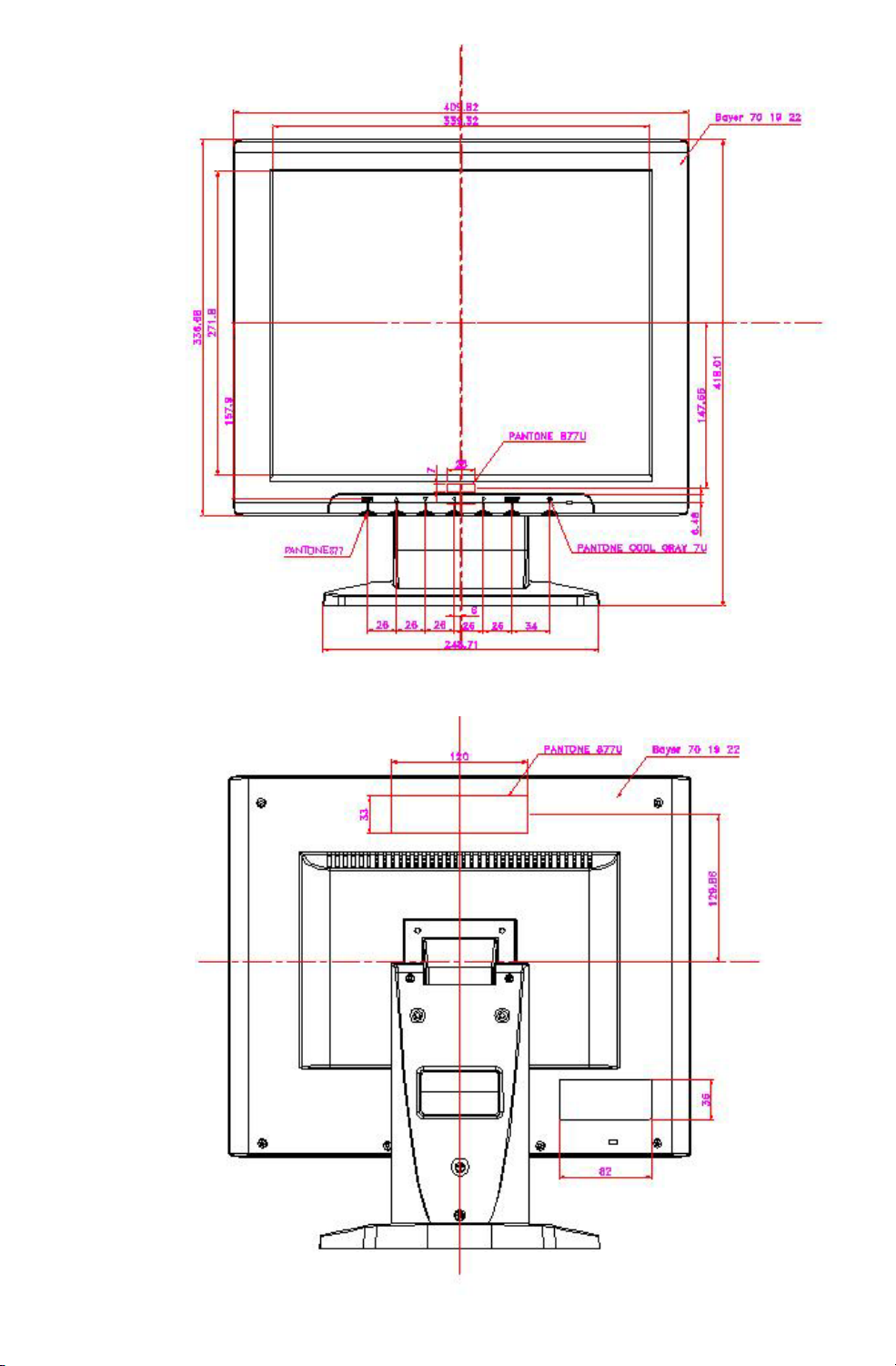
2. MECHANICAL SPECIFICATIONS
2.1 Dimension Height : 418 mm ( 16.5")
Width : 408 mm ( 16")
Depth : 183 mm ( 7.2")
2.2 Net Weight :5.6 kg ( 12.4 lbs)
2.3 Maximum Viewable Area : Diagonal 432 mm
(17")
3. PANEL SPECIFICATIONS
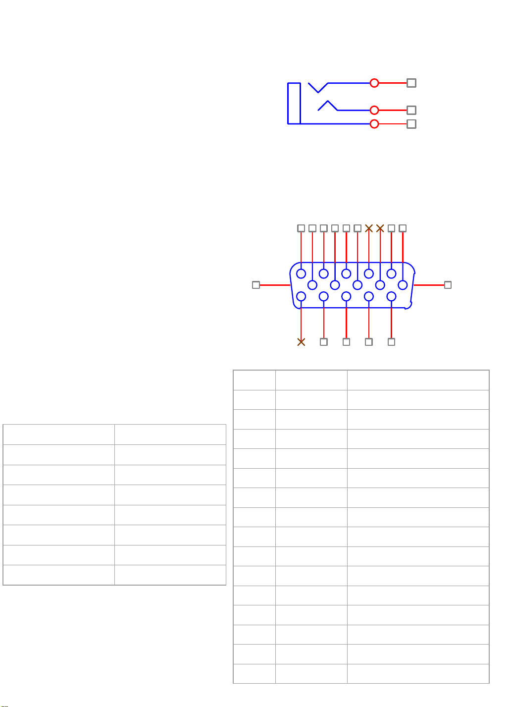
connector x 1
PI
1 RV Red Video
J1
1
2
3
PHONEJACK STEREO
CN6
162738495
16 17
11
12
13
14
10
DB15HD
15
MNEMON SIGNA
Part No. AA0170E1003
Driver bit of panel 8 bit
Contrast ratio 350:1 t
Brightness 250 cd/ m2
Pixel pitch 0.264 mm
Response time < 30 ms (Tr+Tf
View angle 75/75/65/60
Color coordinate x=0.313,y=0.329
4. CONNECTORS
4.1 AC inlet : CEE22 typed connector
2 GV Green Video
3 BV Blue Video
4
one
5 GND Ground(DDC return
6 RG Red GND
7 GG Green GND
8 BG Blue GND
9 +5V + 5V (for DDC
10 SG Sync GND
11
one
12 SDA DDC Data
13 HS Horizontal Sync
14 VS Vertical Syn
15 SCL DDC Cloc
5. ELECTRICAL SPECIFICATIONS 5.4 Preset Timings
5.1 Standard conditions
Display area 338 x 270 mm
Video signal level 0.7 Vpp
Contrast Max.
Brightness Max.
Ambient 20 +/- 5 C degrees
Input voltage AC 120,60Hz
Warming up time > 30 minutes
Display mode 1280 x 1024
5.2 POWER
5.2.1 Power supply
Input voltage 90~240 Volts
Power frequency 50 / 60 Hz, +/-3
Input current < 0.5 A
Inrush current < 1 A
Power < 50 Watts
# mode Resolution Hz (KHz)
1 IBM VGA 720 x 400 70 31.46
2 VESA 640 x 480 60 31.46
”
4 VESA 640 x 480 72 37.86
6 VESA 800 x 600 56 35.16
7 VESA 800 x 600 60 37.87
8 VESA 800 x 600 72 48.07
9 VESA 800 x 600 75 46.87
1
MAC 16” 832 x 624 75 49.72
1
VESA 1024 x 768 60 48.36
1
VESA 1024 x 768 70 56.48
1
VESA 1024 x 768 75 60.02
1
VESA 1152 x 864 75 67.5
1
VESA 1280 x 1024 60 63.98
5.2.2 Power Management
1
VESA 1280 x 1024 75 79.97
State Power Indicator
On < 50Watts Green
Standby < 5 Watts Amber
Off < 5 Watts
5.3 Acceptable timing using 0,7 Vp-p Video signal.
If your timing is within following specification, 5.5.2 Sync Signal level
this LCD display can automatically function with H/V Separate : TTL level
a certain position. 5.5.3 Input impedance
Horizontal: Sync frequency : 30~81 kHz Video input : 75 ohms
Vertical : Sync frequency : 56~75Hz Sync input : > 1 k ohms
5.5 Signal level and input impedance
5.5.1 Video Signal level
This LCD display is adjusted at the factory

5.6 Display Area 6. ENVIRONMENTS
Display area : 338 x 270 mm
Operation Storage and
0 ~ 40 C -20 ~ +60 C
5.7 General performance
5.7.1 Maximum pixel clock
135 MHz
5.7.2 Maximum luminance
Tempera
Humidit 5 ~ 90 %
5 ~ 90 % *
Value 250 cd / m2 at center of the
Altitude 3000m 12000m
display area ,Specified by
6500K + 8 MPCD
Conditions Display image : Full white
Brightness : Maximum
Contrast : Maximum
5.7.3 Brightness variation 7.2 EMC standards
Value 75 % Variation = C / A x 100
Conditions Display image: Full white
Brightness : Maximum
Contrast : Maximum
* Non-condensation
7. REGULATORY STANDARDS
7.1 Safety standards
This monitor applies to various safty & EMI
standards May refer to the logo label
FCC part 15,subpart B , class-B
CE marking
8. OTHERS
TUV (Rheinland)
ISO13406-II pixel fault class 2
TCO99
A: Luminance at center
position
C: Luminance at position of
lowest brightness
5.7.4 Contrast ratio (CR)
Value CR= B / A
Conditions Contrast : Maximum
B: Full white pattern
Brightness : min
A: Full black pattern
Brightness : max
9. P0WER CORD
Northern Hemisphere Version : UL / CSA
approved power cord.
European : VDE approved power cord.
10. SIGNAL CABLE
Signal cable with Mini D-Sub 15P connectors at
both ends.
Length : 1.5 meter.
11. RELIABILITY
11.1 MTBF for completed unit without LCD
> 30,000 hours (demonstrated MTBF)
11.2 MTBF for LCD
The brightness is still more than 50% of the
original brightness after 25,000 hours (min.)
4. THEORY OF OPERATION
r
This section describes the function of the LCD monitor per functional block.
L7EA monitor includes MB board, audio board (option), inverter board, adapter and button board.
4.1 MB BOARD
The MB board is a four-layer, single-landed design with ground and internal planes provided. DC power
from the power adapter enter the board through DC jack. Other connectors on the board are for inverter,
audio and button board .The VGA cable is a signal cable that contains video signal, sync signal and DDC
signal from PC VGA adapter.
This system board consists of 4 functional areas : flat panel controller, flash ROM , power regulator and
LVDS transmitter.
4.1.1 Flat panel controller…… gm2120 (U8)
The heart of the system board is Genesis gm2120. The gm2120 is a graphics processing IC for LCD
monitor. It provides all key IC functions required for LCD panel. On-chip functions include a
high-speed triple-ADC , PLL, high sacling engine, OSD controller and on-chip microcontroller.
a) Clock Generation :
Crystal Input Clock (TCLK and XTAL). This is the input pair to an internal crystal oscillator and
corresponding logic. A 14.318 MHz crystal is recommended.
b) Hardware Reset ( Pin 5 )
Hardware Reset signal is generated by MAX6326 (U10).It assert a reset signal at least 100 ms.
c) Analog to Digital Converter
The gm2120 chip has three ADC's (analog-to-digital converters), one for each color (red, green and blue)
The analog RGB signals are connected to gm2120 as described below
Pin Name Pin Numbe
Red + 171
Red - 170
Green + 167
Green - 166
Blue + 163
Blue - 162
d) OSD :
The gm2120 has a fully programmable ,high-quality OSD controller.The on-chip static RAM(4096 words
by 24 bits) stores the cell map and the cell definitions.
e) On-Chip Microcontroller (OCM)
The gm2120 on-chip microcontroller(OCM) serves as the system microcontroller.That is , it programs the
gm2120 and manages other devices in the system such as the keypad, the backlight, LED, audio and
non-volatile RAM.using general purpose input/output (GPIO) pins.

2
Pin Number Pin Name Pin Usage
l
t
R
p
t
n
n
ge
l
u
N
N
A
N
L
n
N
L
N
N
l
Qn
n
K
N
A
40 GPIO0 / PWM0 Backlight contro
41 GPIO1 / PWM1 Volume control
42 GPIO2 / PWM2 Key-Lef
43 GPIO3 / TIME
44 GPIO4 / UART_DI Debug Purpose
45 GPIO5 / UART_DO Debug Purpose
46 GPIO6 Key-Righ
47 GPIO7 Key-Dow
39 GPIO8 / IRQIN
48 GPIO9 Key-Se
49 GPIO10 Key-Men
50 GPIO11
51 GPIO12
52 GPIO13
205 GPIO16 / HFS
1 GPIO17
208 GPIO18
207 GPIO19 Key-Power, on / off contro
Key-U
LED-Oran
o use
V- RAM (U4) SD
V- RAM (U4) SC
V- RAM (U11) SC
o use
o use
206 GPIO20 Mute , audio disable
4 GPIO21 / IR
204 GPIO22 / HCL
f) Panel Power Sequencing ( PPWR, PBIAS) ( Pin 113~114)
0 has two dedicated outputs PPWR and PBIAS ( Pin113 and Pin114) to control LCD power
sequencing once data and control signals are stable.
g) Parallel ROM Interface Port (Pin 8~25, Pin28~35)
The gm2120 has parallel ROM interface port , pin8~25 for address bus, pin28~35 for data bus.
h) Panel interface (Pin 55~66, Pin69~80, Pin83~87, Pin90~96.Pin99~110)
The gm2120 driver interface is highly programmable. It supports dual bus / dual port for SXGA drivers.
4.1.2 LVDS Transmitter DS90C383 (U1,U2)
The DS90C383 transmitter converts 28 bits of TTL data into four LVDS ( Low Voltage Differential
Signaling) data streams. A phase-locked transmit clock is transmitted in parallel with the data streams
over a fifth LVDS link. At a transmit clock frequency of 85 MHz, 24 bits of RGB data and 3 bits of LCD
timing and control data ( FPLINE, FPFRAME, DRDY) are transmitted at rate of 595 Mbps per LVDS
data channel. U1 AS the ODD pixel transmitter , U2 as the EVEN pixel transmitter.
LED-Gree
V- RAM (U11) SD
4.1.3 Power Regulator AIC1563 (U12),LT1117 (U5, U6)
ge
t
r
y
The AIC1563 is a monolithic control IC containing the primary functions required for DC to DC converters.
The device consists of an internal temperature compensated reference, conparator, controlled duty cycle
oscillator with an active current sense circuit. Desired output voltage are determined by the equation
Vout = 1.25 ( 1 + R104 / R103), In this case, the output voltage are 5 Volts.
The AIC1117 is a low dropout positive adjustable regulator with minumum of 1A output current capability.
So it is well suited for 3.3 V and 2.5 V Rregulator.
U6 as a 2.5 V regulator , Desired output voltage are determined by the equation
Vout=5 x ( R53 / R53+R56)= 2.5
U5 as a 3.3 V regulator , Desired output voltage are determined by the equation
Vout=5 x ( R30 / R30+R36)= 3.3
4.2 Audio Board AN7522 (U1)
The AN7522 is a 2 channel audio power amplifier capable of delivering 2W of continuous average power
to an 8 ohms with less than 0.5% (THD) from a 12 V power supply.
An7522 can directly drive 8 ohms speaker , does not require output coupling capacitor, bootstrap capacitor
,or snubber network. Audio line-in are feed into pin 6,8 of the AN7522. The output power is controlled by
the DC voltage of pin 8 from gm2120 GPIO port.
4.3 Inverter Board
This is a specific inverter for L7E monitor backlight which converters 12 Vdc to drive four cold cathod
fluorescence tubes. Electrical specification describled as below.
INPUT
OUTPUT
Rated Input Volta
Maximum Input Voltage 11.4~12.6 Vdc
Input Curren
Off state Input Powe
On / Off Voltage 2~3.3 for On, 0~1 for Off
Rated Output Strike-on Voltage 1310 Vrms
Rated Output Voltage 710 Vrms at 6 mA
Rated Output Frequenc
Rate Output Current per tube 6 mA
12Vdc
< 2A
< 0.1 W
45~60KHz

4.4 Adapter
ge
t
)
r
n
p
t
y
d
This is a general purpose AC / DC adapter which converter 90~240 Vac to a stabilized DC voltage 12 V
with rated output current of 4.16A . Electrical specification describled as below.
INPUT
OUTPUT
Rated Input Voltage 90~240 Vac , 50/60 Hz
Operation Input Volta
Input Curren
Inrush Current (Cold Start
Standby Input Powe
Rated Output Voltage 12 Vdc
Output Voltage Regulatio
Output Ripple and Noise < 600 mVp-
Rate Output Curren
Turn-on Dela
90~260 Vac, 47~63 Hz
< 1.5A
< 100A @ 120Vac
< 1.5 W at 120Vac
+ 10 / -5 %
< 4.16A
< 1 Secon
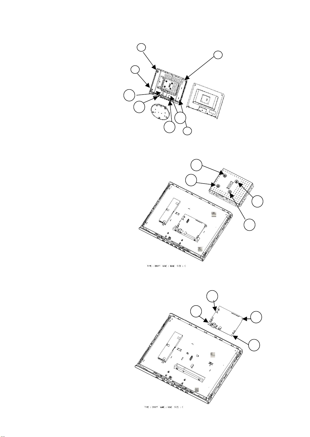
5. DISASSEMBLY INSTRUCTIONS
1. Stand& rear cover removal
1) remove four large screw "1" from
the rear cover
2) remove the rear cover
3) remove four screw "2"
4) remove the stand
2
2
2. ESD cover removal
1) remove four screw "3"
2) remove the ESD cover
2
2
3
3
3
3
3. MB board removal
1) remove four screw "4"
2) remove the MB board
4
4
4
4
 Loading...