

Page 1

Acer AL2616Wv
Service Guide
1
Page 2
Service Guide Version and Revision
Version Release Date Revision History TPV model
A00 Sep-29-2006 Initial Release TE6GMHDBWBABNP
2
Page 3
Copyright
Copyright © 2006 by Acer Incorporated. All rights reserved. No part of this publication may be reproduced,
Transmitted, transcribed, stored in a retrieval system, or translated into any language or computer language, in
any form or by any means, electronic, mechanical, magnetic, optical, chemical, manual or otherwise, without
the prior written permission of Acer Incorporated.
Disclaimer
The information in this guide is subject to change without notice. Acer Incorporated makes no representations or
warranties, either expressed or implied, with respect to the contents hereof and specifically disclaims any warranties
of merchantability or fitness for any particular purpose. Any Acer Incorporated software described in this manual is
sold or licensed "as is". Should the programs prove defective following their purchase, the buyer (and not Acer
Incorporated, its distributor, or its dealer) assumes the entire cost of all necessary servicing, repair, and any
incidental or consequential damages resulting from any defect in the software.
Intel is a registered trademark of Intel Corporation.
Pentium and Pentium II/III are trademarks of Intel Corporation.
Other brand and product names are trademarks and/or registered trademarks of their respective holders.
Trademarks
Acer is a registered trademark of Acer Incorporated.
All other trademarks are property of their respective owners.
Conventions
The following conventions are used in this manual:
Screen messages Denotes actual messages that appear on screen.
Note Gives bits and pieces of additional information related to the current topic.
Warning Alerts you to any damage that might result from doing or not doing specific
actions.
Caution Gives precautionary measures to avoid possible hardware or software
problems.
Important Remind you to do specific actions relevant to the accomplishment of
procedures.
3
Page 4

Preface
Before using this information and the product it supports, please read the following general information.
1. This Service Guide provides you with all technical information relating to the BASIC CONFIGURATION decided
for Acer's "global" product offering. To better fit local market requirements and enhance product competitiveness,
your regional office may have decided to extend the functionality of a machine (e.g. add-on card, modem, or extra
memory capability). These LOCALIZED FEATURES will NOT be covered in this generic service guide. In such
cases, please contact your regional offices or the responsible personnel/channel to provide you with further
technical details.
2. Please note WHEN ORDERING FRU PARTS, that you should check the most up-to-date information available on
your regional web or channel. If, for whatever reason, a part number change is made, it will not be noted in the
printed Service Guide. For ACER-AUTHORIZED SERVICE PROVIDERS, your Acer office may have a
DIFFERENT part number code to those given in the FRU list of this printed Service Guide. You MUST use the list
provided by your regional Acer office to order FRU parts for repair and service of customer machines.
Warning: (For FCC Certified Models)
Note: This equipment has been tested and found to comply with the limits for a Class B digital device, pursuant to
Part 15 of the FCC Rules. These limits are designed to provide reasonable protection against harmful interference in
a residential installation. This equipment generates, uses and can radiate radio frequency energy, and if not installed
and used in accordance with the instructions, may cause harmful interference to radio communications. However,
there is no guarantee that interference will not occur in a particular installation. If this equipment does cause harmful
interference to radio or television reception, which can be determined by turning the equipment off and on, the user
is encouraged to try to correct the interference by one or more of the following measures:
1. Reorient or relocate the receiving antenna.
2. Increase the separation between the equipment and receiver.
3. Connect the equipment into an outlet on a circuit different from that to which the receiver is connected.
4. Consult the dealer or an experienced radio/TV technician for help.
Notice:
1. The changes or modifications not expressly approved by the party responsible for compliance could void the
user's authority to operate the equipment.
2. Shielded interface cables and AC power cord, if any, must be used in order to comply with the emission limits.
3. The manufacturer is not responsible for any radio or TV interference caused by unauthorized modification to this
equipment. It is the responsibility of the user to correct such interference.
®
As ENERGY STAR
Partner our company has determined that this product meets the ENERGY STAR
guidelines for energy efficiency.
®
Warning:
To prevent fire or shock hazard, do not expose the monitor to rain or moisture. Dangerous high voltages are
present inside the monitor. Do not open the cabinet. Refer servicing to qualified personnel only.
4
Page 5

Precautions
z
Do not use the monitor near water, e.g. near a bathtub, washbowl, kitchen sink, laundry tub, swimming pool or in
a wet basement.
z Do not place the monitor on an unstable trolley, stand, or table. If the monitor falls, it can injure a person and
cause serious damage to the appliance. Use only a trolley or stand recommended by the manufacturer or sold
with the monitor. If you mount the monitor on a wall or shelf, uses a mounting kit approved by the manufacturer
and follow the kit instructions.
z Slots and openings in the back and bottom of the cabinet are provided for ventilation. To ensure reliable
operation of the monitor and to protect it from overheating, be sure these openings are not blocked or covered.
Do not place the monitor on a bed, sofa, rug, or similar surface. Do not place the monitor near or over a radiator
or heat register. Do not place the monitor in a bookcase or cabinet unless proper ventilation is provided.
z The monitor should be operated only from the type of power source indicated on the label. If you are not sure of
the type of power supplied to your home, consult your dealer or local power company.
z The monitor is equipped with a three-pronged grounded plug, a plug with a third (grounding) pin. This plug will fit
only into a grounded power outlet as a safety feature. If your outlet does not accommodate the three-wire plug,
have an electrician install the correct outlet, or use an adapter to ground the appliance safely. Do not defeat the
safety purpose of the grounded plug.
z Unplug the unit during a lightning storm or when it will not be used for long periods of time. This will protect the
monitor from damage due to power surges.
z Do not overload power strips and extension cords. Overloading can result in fire or electric shock.
z Never push any object into the slot on the monitor cabinet. It could short circuit parts causing a fire or electric
shock. Never spill liquids on the monitor.
z Do not attempt to service the monitor yourself; opening or removing covers can expose you to dangerous
voltages and other hazards. Please refer all servicing to qualified service personnel
z To ensure satisfactory operation, use the monitor only with UL listed computers which have appropriate
configured receptacles marked between 100 - 240V AC, Min. 5A.
z The wall socket shall be installed near the equipment and shall be easily accessible.
Special Notes On LCD Monitors
The following symptoms are normal with LCD monitor and do not indicate a problem.
Notes
z Due to the nature of the fluorescent light, the screen may flicker during initial use. Turn off the Power Switch and
then turn it on again to make sure the flicker disappears.
z You may find slightly uneven brightness on the screen depending on the desktop pattern you use.
z The LCD screen has effective pixels of 99.99% or more. It may include blemishes of 0.01% or less such as a
missing pixel or a pixel lit all of the time.
z Due to the nature of the LCD screen, an afterimage of the previous screen may remain after switching the image,
when the same image is displayed for hours. In this case, the screen is recovered slowly by changing the image
or turning off the Power Switch for hours.
5
Page 6

Table Of Contents
Chapter 1 Monitor Features ………………………………………… 6
Chapter 2 Operating Instructions ……………………………………… 21
Introduction ……………………………………… 7
Electrical Requirements ……………………………………… 8
LCD Monitor General Specification ……………………………………… 9
LCD Panel Specification ……………………………………… 11
Support Timing ……………………………………… 13
Monitor Block Diagram ……………………………………… 14
Main Board Diagram ……………………………………… 15
Software Flow chart ……………………………………… 16
Main Board Layout ……………………………………… 18
Front Bezel ……………………………………… 19
Rear Bezel ……………………………………… 20
External Controls ……………………………………… 21
Front Panel Controls ……………………………………… 22
Adjusting the picture ……………………………………… 23
Hot-Key Menu ……………………………………… 26
OSD Message ……………………………………… 26
LOGO ……………………………………… 27
Chapter 3 Machine Disassembly ………… …………………………… 28
Chapter 4 Troubleshooting ……………………………………… 34
Chapter 5 Connector Information ………………………… …………… 39
Chapter 6 FRU (Field Replacement Unit) List ……………………………………… 40
Chapter 7 Schematic Diagram ……………………………………… 44
Exploded Diagram ……………………………………… 41
6
Page 7
Monitor Features
Chapter 1
Introduction
Scope
This specification defines the requirements for the 19” MICROPROCESSOR based Multi-mode supported high
resolution color LCD monitor. This monitor can be directly connected to general 15-pin D-sub VGA connector and
24-pin DVI connector, also supports VESA DPMS power management and plug & play function. There is a build-in
stereo audio amplifier with OSD control to drive a pair of speakers.
Description
The LCD monitor is designed with the latest LCD technology to provide a performance oriented product with no
radiation. This will alleviate the growing health concerns. It is also a space saving design, allowing more desktop
space, and comparing to the traditional CRT monitor, it consumes less power and gets less weight in addition MTBF
target is 50k hours or more.
Chart of AL2616W
Panel
LM260wu1
Signal Interface
Sync Type
Color Temp User Adjust
DDC
Speaker
D-Sub 15-pin
DVI 24-pin
Separate / Compatible
Support
DDC2B
No
Headphone Jack
Microphone Jack
USB Hub
No
No
Not support
Tilt / Swivel
Yes / No
7
Page 8
Electrical Requirements
Standard Test Conditions
All tests shall be performed under the following conditions, unless otherwise specified.
Ambient light
Viewing distance
Warm up time
All specifications :
Fully functional : 5 seconds
Measuring equipment
Control settings
User brightness control : Set to Factory preset value (cut off raster)
User contrast control : T Set to factory preset value, which allows that the brightest two
User red/white balance,
Green/white balance and
: Dark room
: 40 cm for LCD performance, 20 cm for LCD failures
>30 minutes
: Chroma 7120 signal generator or equivalent, directly
Connected to the monitor under test.
Minolta CA100 photometer, or equivalent
of 32 linear distributed gray-scales (0~ 700mv) can be
distinguished.
Blue/white balance control : In the center (unless otherwise specified)
Power input
Ambient temperature
Display mode
:
:
: 1680x1050, 60 Hz, all white
230V± 5%
+5℃
20
Measurement systems
The units of measure stated in this document are listed below:
1 gamma = 1 nano tesla
1 tesla = 10,000 gauss
cm = in x 2.54
Lb = kg x 2.2
Degrees F = [°C x 1.8] + 32
Degrees C = [°F - 32]/1.8
u' = 4x/(-2x + 12y + 3)
v' = 9y/(-2x + 12y + 3)
x = (27u'/4)/[(9u'/2) - 12v' + 9]
y = (3v')/[(9u'/2) - 12v' + 9]
nits = cd/(m2) = Ft-L x 3.426
lux = foot-candle x 10.76
8
Page 9
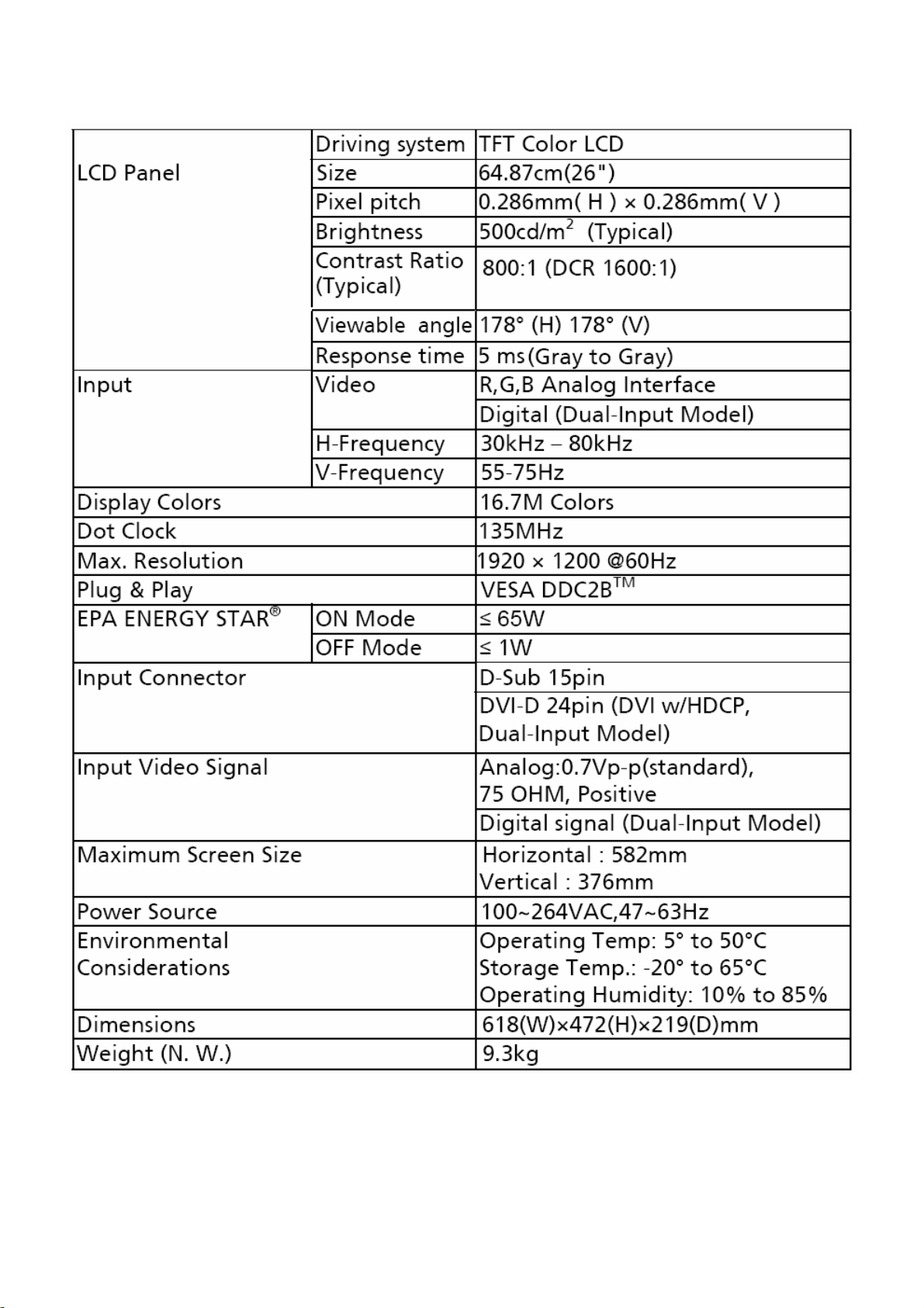
LCD Monitor General Specification
9
Page 10
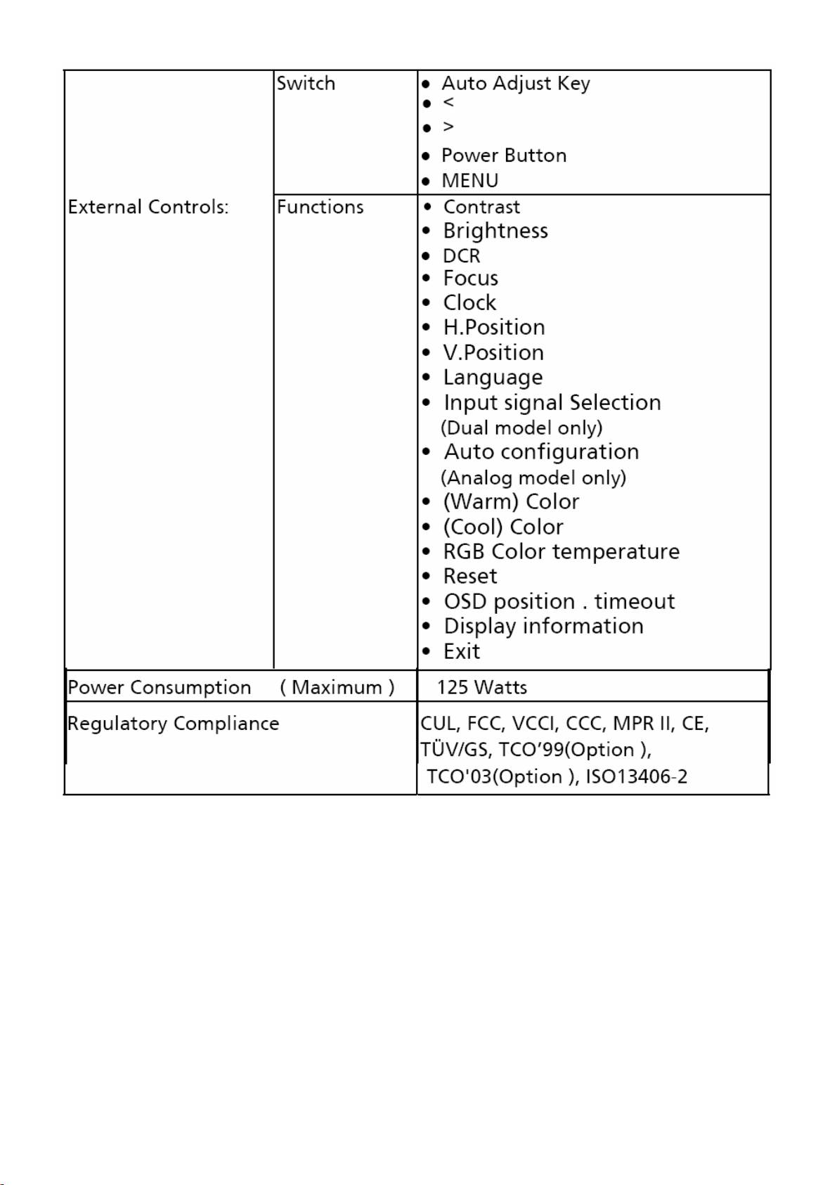
10
Page 11
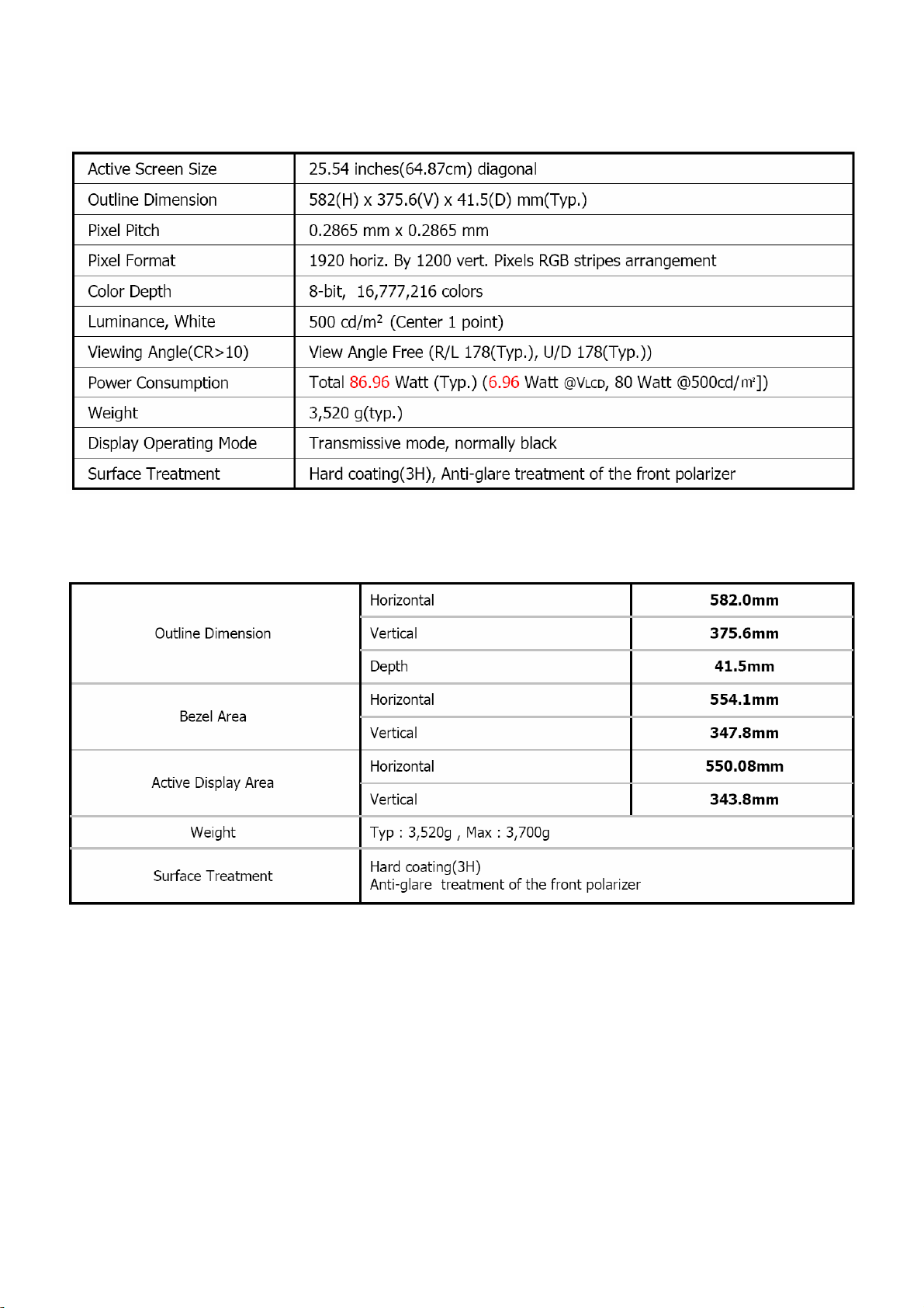
LCD Panel Specification
General Specifications
Mechanical Characteristics
11
Page 12
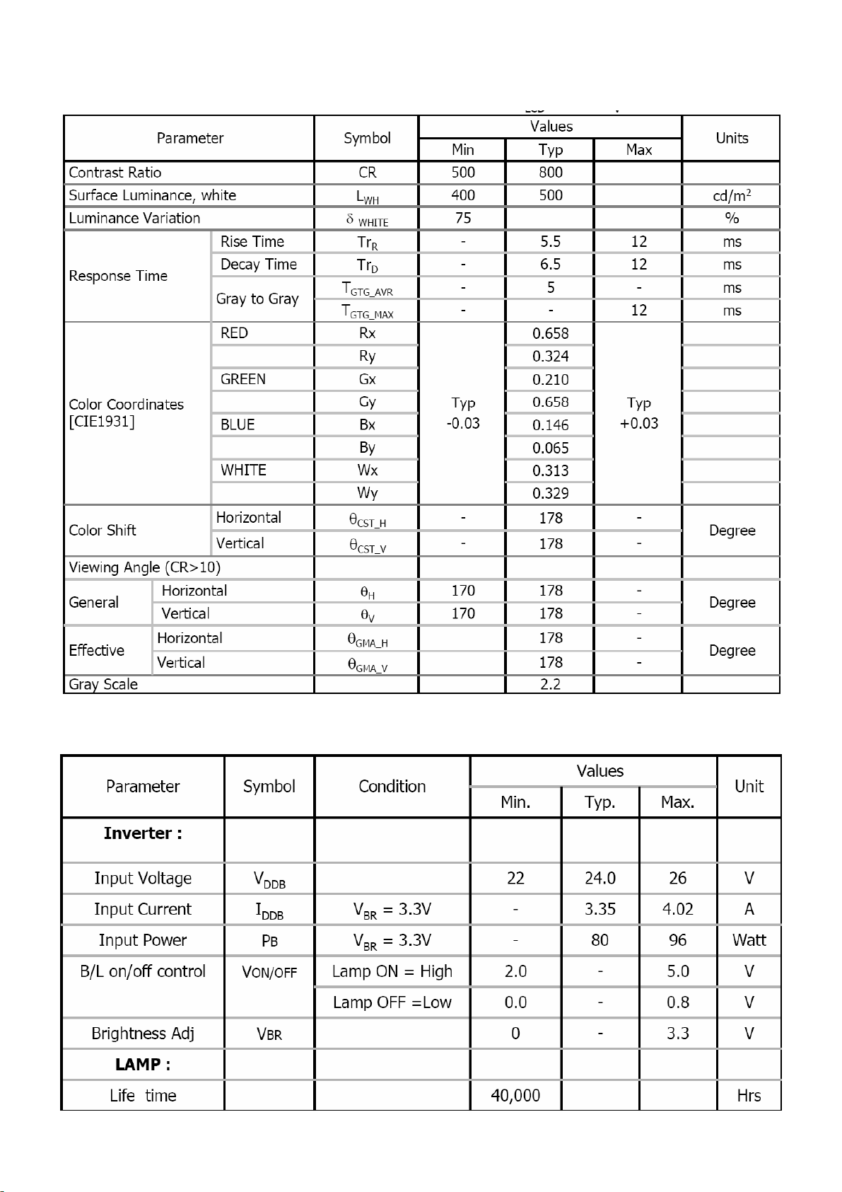
Optical Specifications
Inverter Electrical characteristics
12
Page 13
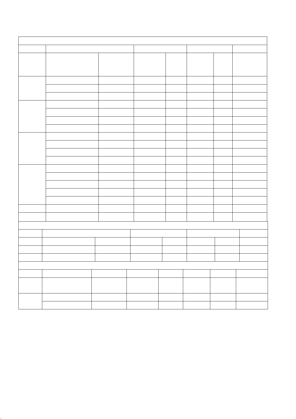
Supported Timing
VESA MODES
Horizontal Vertical
Nominal
Mode Resolution Total
640x480@60Hz 800 x 525 31.469 N 59.940 N 25.175
VGA
SVGA
XGA
SXGA
1440x900@60Hz 1904x934 55.93 P 60 P 106.5
WSXGA
640x480@72Hz 832 x 520 37.861 N 72.809 N 31.500
640x480@75Hz 840 x 500 37.500 N 75.00 N 31.500
800x600@56Hz 1024 x 625 35.156 N/P 56.250 N/P 36.000
800x600@60Hz 1056 x 628 37.879 P 60.317 P 40.000
800x600@72Hz 1040 x 666 48.077 P 72.188 P 50.000
800x600@75Hz 1056x625 46.875 P 75.000 P 49.500
1024x768@60Hz 1344x806 48.363 N 60.004 N 65.000
1024x768@70Hz 1328x806 56.476 N 70.069 N 75.000
1024x768@72Hz 1304x798 57.7 P 72 P 78.4
1024x768@75Hz 1312x800 60.023 P 75.029 P 78.750
1280x1024@60Hz 1688x1066 63.981 P 60.020 P 108.000
1280x1024@70Hz 1688x1066 74.4 P 70 P 124.9
1280x1024@72Hz 1688x1066 77.9 P 72 P 134.6
1280x1024@75Hz 1688x1066 79.976 P 75.025 P 135.000
1280x960@60Hz 1800x1000 60 P 60 P 108
1680x1050@60Hz 2240x1089 65.29 N 59.95 P 146.25
Frequency
+/- 0.5kHz
Sync
Polarit
y
Nominal
Freq.
+/- 1 Hz
Sync
Polari
ty
Nominal
Pixel Clock
(MHz)
IBM MODES
Horizontal Vertical
DOS 720x400@70Hz 900 x 449 31.469 N 70.087 P 28.322
DOS 640x350@70Hz 800 x 449 31.469 P 70.087 N 25.175
XGA 1024x768@72Hz 1304 x 798 57.515 P 72.1 P 75.000
MAC MODES
VGA
SVGA
640x480@67Hz 864x525 35.000 N 66.667 N 30.240
832x624@75Hz 1152x667 49.725 N 74.551 N 57.2832
1024x768@60Hz 1312x813 48.780 N 60.001 N 64.000 XGA
1024x768@75Hz 1328x804 60.241 N 74.927 N 80.000
13
Page 14
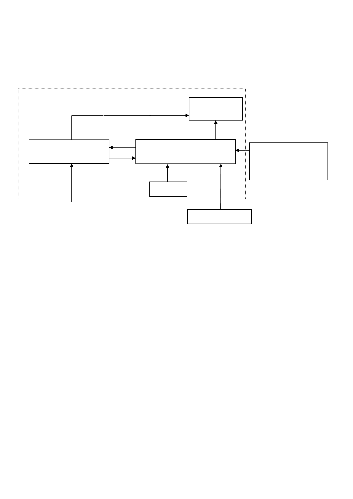
Monitor Block Diagram
The LCD MONITOR will contain a main board, a power board, and keypad board which house the flat panel control
logic, brightness control logic and DDC.
The Inverter board will drive the backlight of panel and the DC-DC conversion,
The Adapter will provides the 12V DC-power to inverter/power board.
Flat Panel and
CCFL
backlight
CCFL Drive.
Power Board
(Inverter, adapter Board)
Main Board
RS232 Connector For
white balance adjustment
in factory mode
Keyboard
AC-IN
100V-240V
HOST Computer
Video signal, DDC
14
Page 15
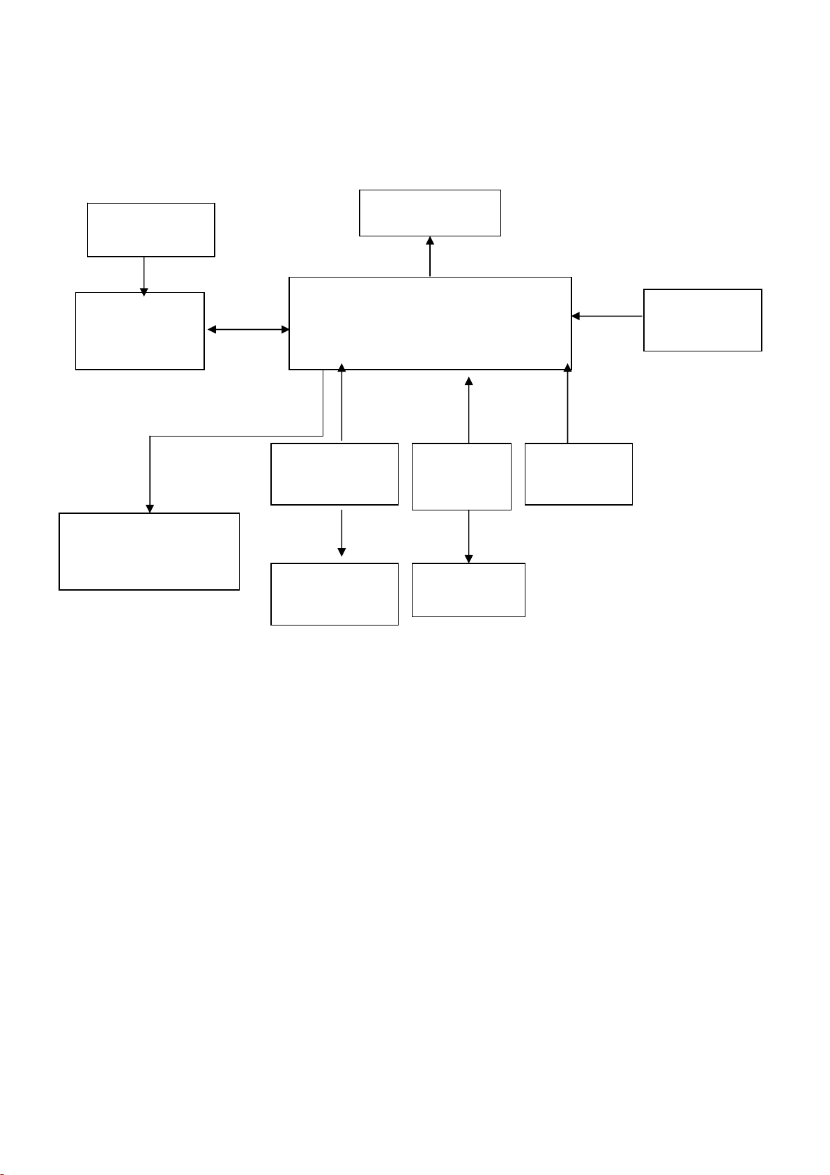
Main Board Diagram
Crystal
24.576MHZ
MCU
MTV416GMV
OSD Control
Interface (Keypad)
Scalar MST9251HA-LF
(Include: ADC, OSD etc)
D-SUB
Connector
EEPROM
24C02
LCD Interface
DVI
Connector
EEPROM
24C02
EEPROM
AT24C16N
Crystal
14.318MHZ
15
Page 16
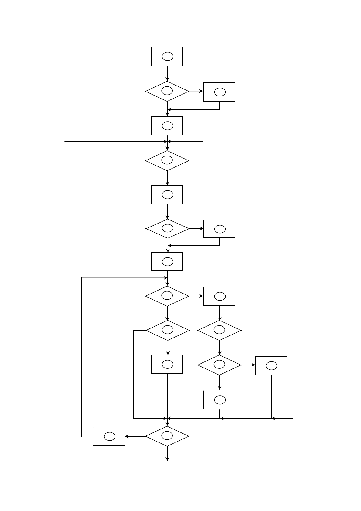
Software Flow Chart
18
N
N
10
12
14
19
1
Y
2
N
4
N
5
Y
6
N
7
Y
9
N
Y
Y
Y
11
13
15
17
3
8
N
Y
N
16
Y
16
Page 17
Remark:
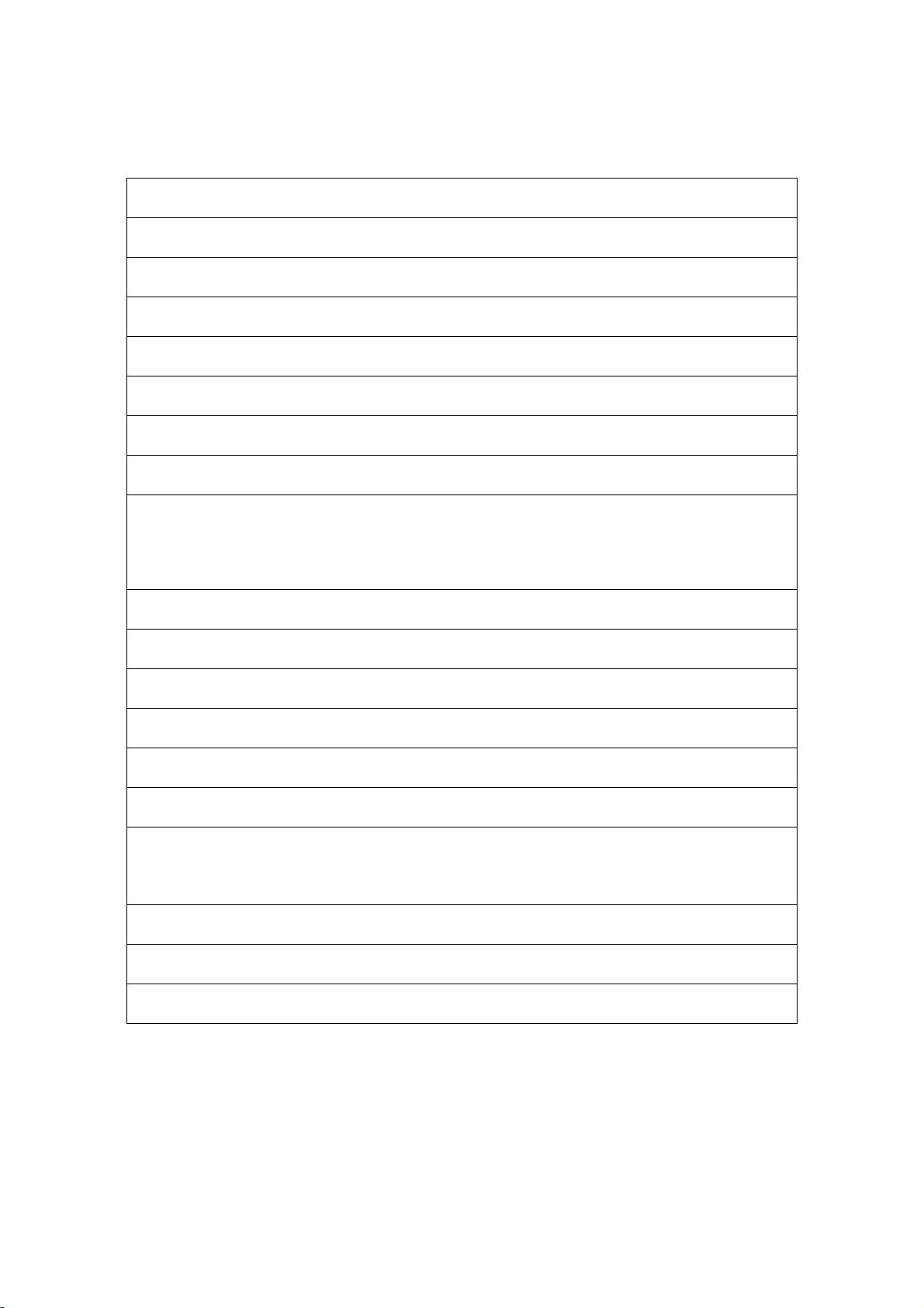
1) MCU initializes.
2) Is the EEPROM blank?
3) Program the EEPROM by default values.
4) Get the PWM value of brightness from EEPROM.
5) Is the power key pressed?
6) Clear all global flags.
7) Are the AUTO and SELECT keys pressed?
8) Enter factory mode.
9) Save the power key status into EEPROM.
Turn on the LED and set it to green color.
Scalar initializes.
10) In standby mode?
11) Update the lifetime of back light.
12) Check the analog port, are there any signals coming?
13) Does the scalar send out an interrupt request?
14) Wake up the scalar.
15) Are there any signals coming from analog port?
16) Display "No connection Check Signal Cable" message. And go into standby mode after the
message disappears.
17) Program the scalar to be able to show the coming mode.
18) Process the OSD display.
19) Read the keyboard. Is the power key pressed?
17
Page 18
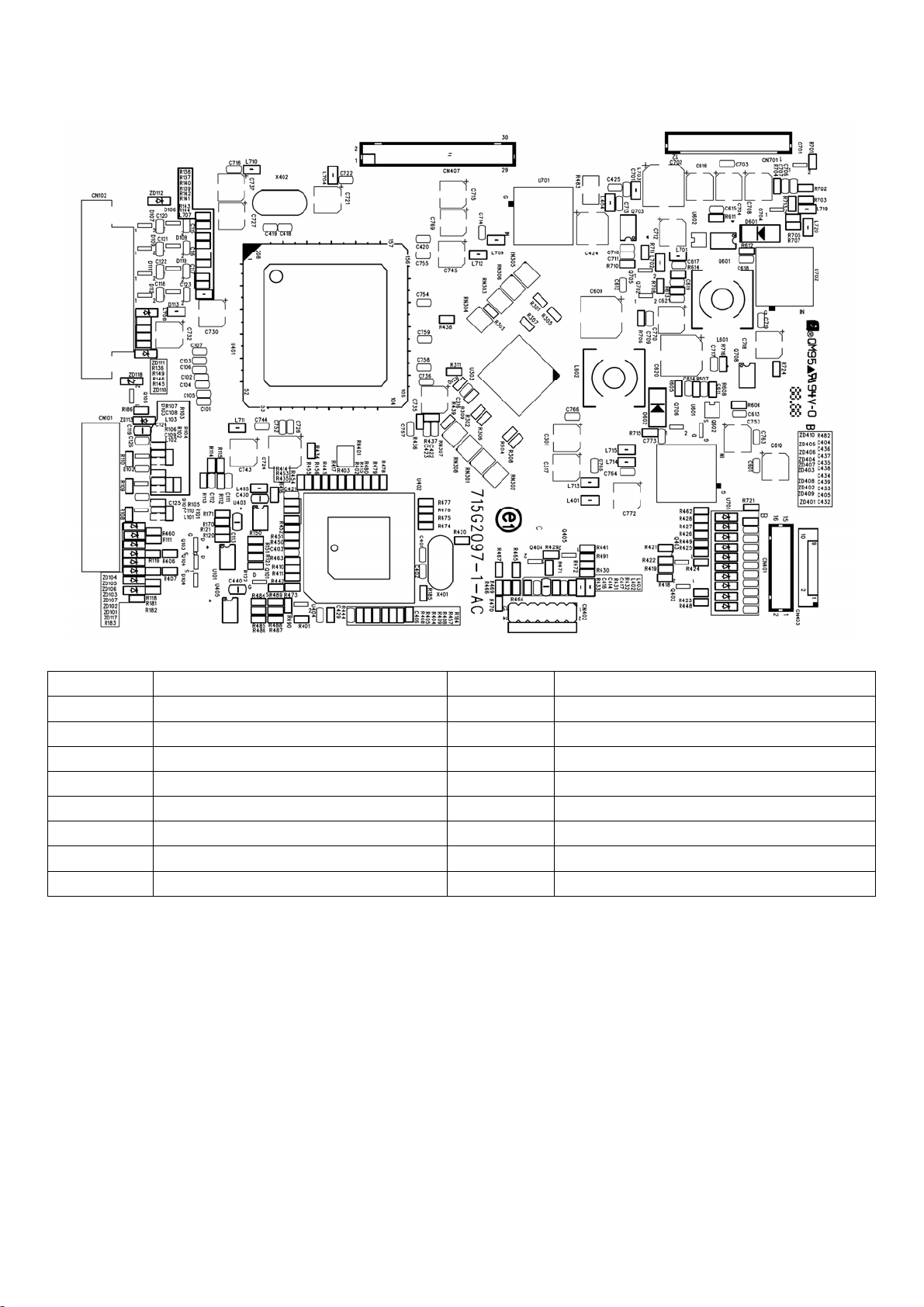
Main Board Layout
Symbol Description Symbol Description
U401 IC MST9251HA-LF-205 PQFP-208 MST U303 EM6A9320BI-5MG FBGA-144
U404
U705 GM6605-2.5TA3R TO-263 GAMMA CN401 WAFER 16PIN 2.0mm DIP
U101 M24C02-WMN6TP CN701 WAFER PH-12
U402 MTV416GMV CN407 WAFER 30P 2.0MM RIGHT ANGLE
U405 CAT24WC08W SOIC-8 CN102 DV1 CONNECTOR 24PIN
U701 GM6605-3.3TA3 CN101 D-SUB 15PIN
U702 GM6605-3.3TA3 CN403 WAFER 2*5P 2.0MM R/A
*G690H293T73 SOT-23 RN305 RST CHIP AR 8P4R 100 OHM +-5% 1/16W
18
Page 19
Chapter 2
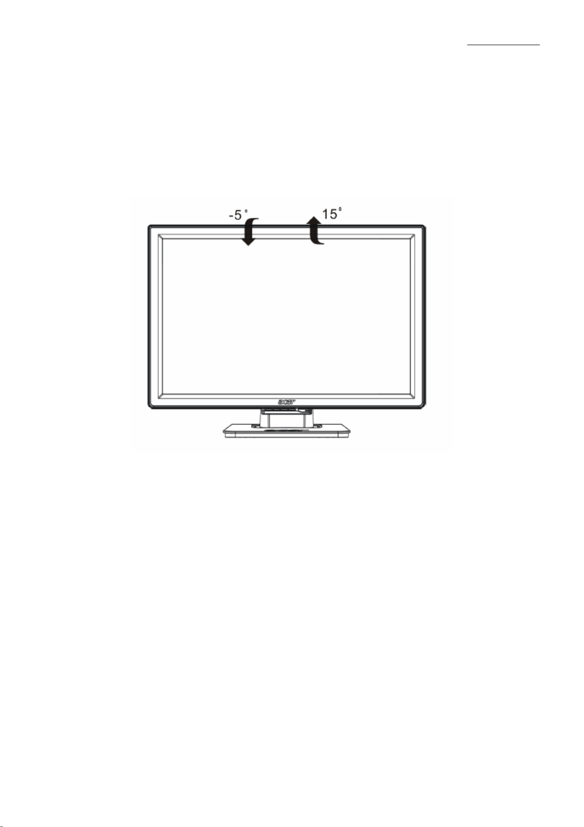
Adjusting the viewing angle
•
For optimal viewing it is recommended to look at the full face of the monitor, then adjust the monitor’s angle to your own
preference.
• Hold the stand so you do not topple the monitor when you change the monitor’s angle.
• You can able to adjust the monitor’s angle from -5° to 15°,
NOTES
• Do not touch the LCD screen when you change the angle. It may cause damage or break the LCD screen.
• Careful attention is required not to catch your fingers or hands when you change the angle.
19
Page 20
Rear Bezel
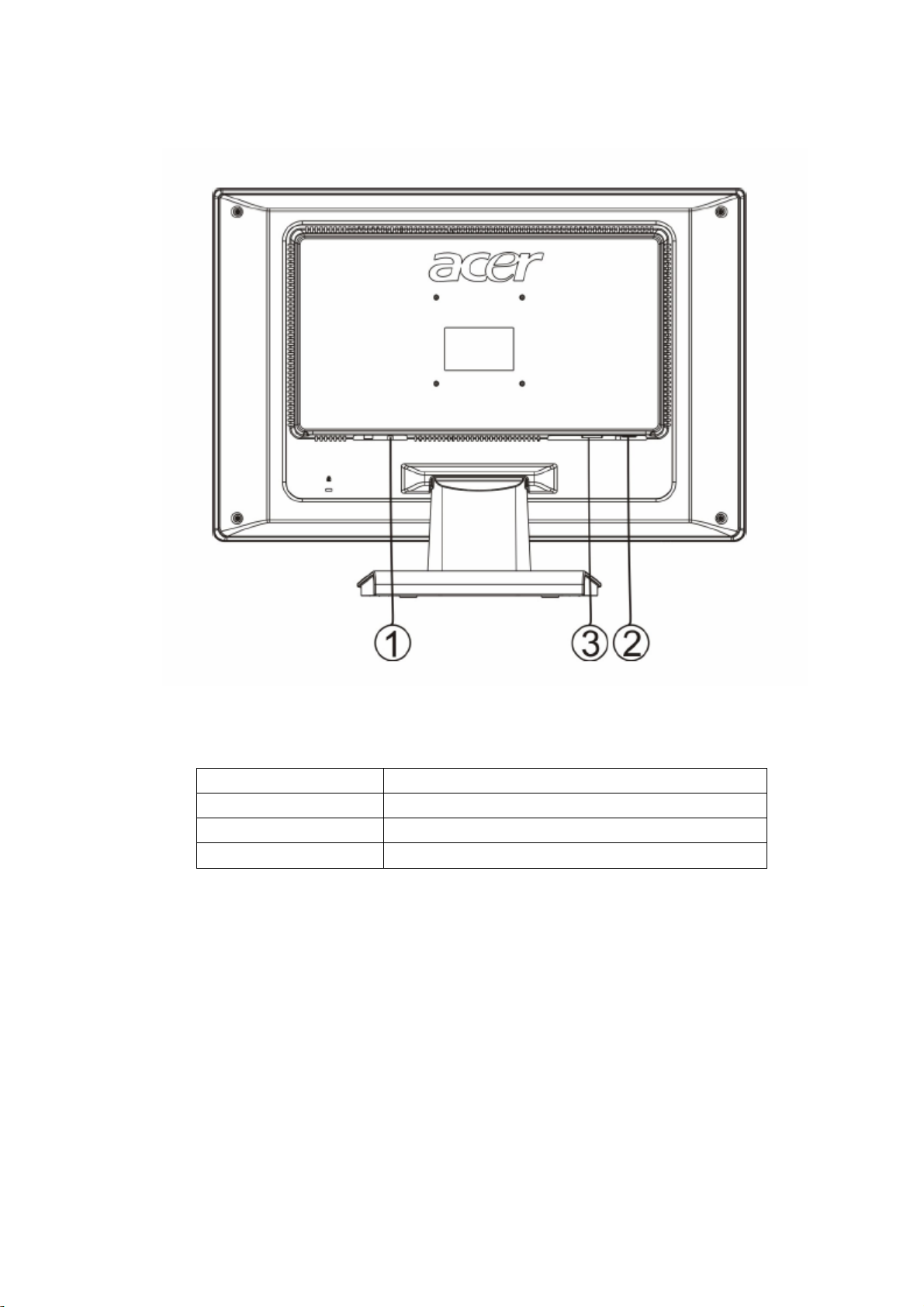
Item Description
1. Power Cable
2. Signal Cable
3. DVI Cable (Only dual-input model)
20
Page 21
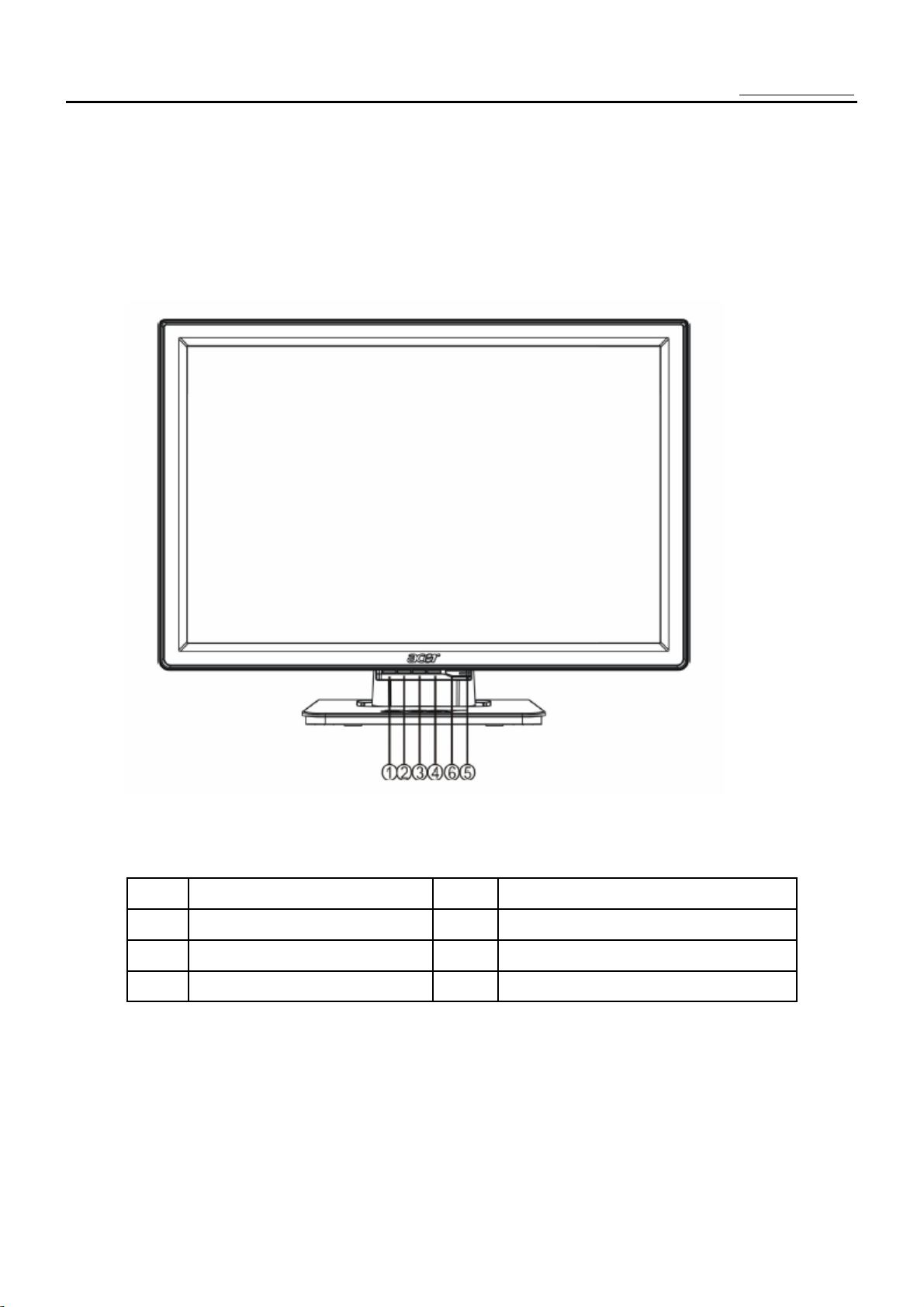
Operating Instructions
Press the power button to turn the monitor on or off. The other control buttons are located at front panel of the
monitor. By changing these settings, the picture can be adjusted to your personal preferences.
• The power cord should be connected.
• Connect the video cable from the monitor to the video card.
• Press the power button to turn on the monitor position. The power indicator will light up.
Chapter 2
External Controls
Item Description Item Description
1. Auto Config / Exit 4. MENU/ENTER
2. < 5. Power Indicator
3. > 6. Power Button
21
Page 22

Front Panel Control
• Power Button:
Press this button to turn the monitor ON or OFF. And display the monitor’s state.
• Menu / Enter:
Activate OSD menu when OSD is OFF or activate/de-activate adjustment function when OSD is ON .
• <:
Navigate through adjustment icons when OSD is ON or adjust a function when function is activated.
• >:
navigate through adjustment icons when OSD is ON or adjust a function when function is activated.
• Auto Adjust button / Exit:
1. When OSD menu is in active status, this button will act as EXIT-KEY (EXIT OSD menu).
2.When OSD menu is in off status, press this button for 2 seconds to activate the Auto Adjustment function.
The Auto Adjustment function is used to set the HPos, VPos, Clock and Focus.
• Power Indicator:
Blue — Power On mode.
Orange — Off mode
NOTES
Notes
• Do not install the monitor in a location near heat sources such as radiators or air ducts, or in a place subject to
direct sunlight, or excessive dust or mechanical vibration or shock.
• Save the original shipping carton and packing materials, as they will come in handy if you ever have to ship your
monitor.
• For maximum protection, repackage your monitor as it was originally packed at the factory.
• To keep the monitor looking new, periodically clean it with a soft cloth. Stubborn stains may be removed with a
cloth lightly dampened with a mild detergent solution. Never use strong solvents such as thinner, benzene, or
abrasive cleaners, since these will damage the cabinet. As a safety precaution, always unplug the monitor before
cleaning it.
22
Page 23
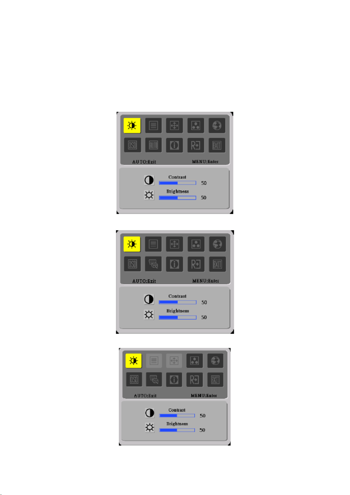
Adjusting the Picture
How to Adjust a Setting
1. Press the MENU-button to activate the OSD window.
2. Press <or >to select the desired function.
3. Press the MENU-button to select the function that you want to adjust.
4. Press < or >to change the settings of the current function.
5. To exit and save, select the exit function. If you want to adjust any other function, repeat steps 2-4
Only Analog Input model
Dual-input model,Analog Input
Dual-input model,Digital Input
23
Page 24
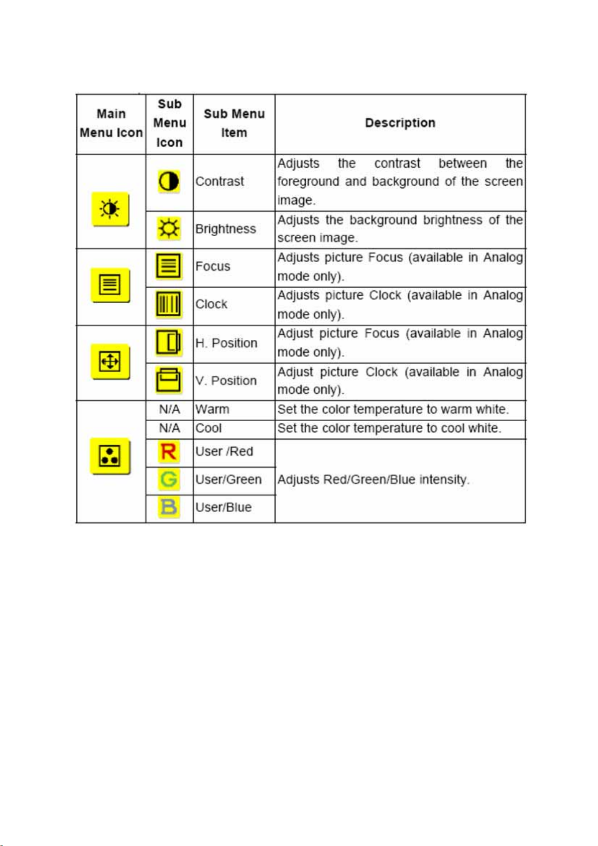
b. The Description For Control Function
24
Page 25
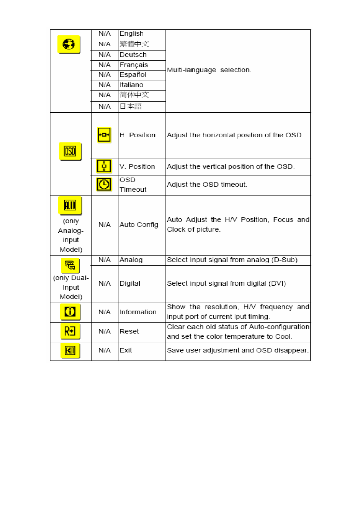
25
Page 26
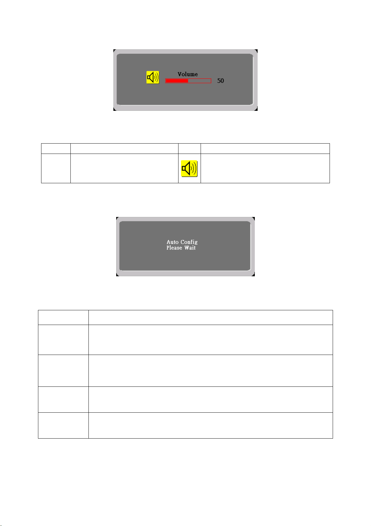
Hot-Key Menu
a. Outline
b. The Description For Hot-Key Function
Item Operation Icon Description
When the OSD is closed, press Left or
Volume
Right button will be Volume Hot-Key
Function
OSD Message
a. Outline
Volume of Audio adjustment. The Audio will be
Mute when volume=0
b. The Description For OSD Message
Item Description
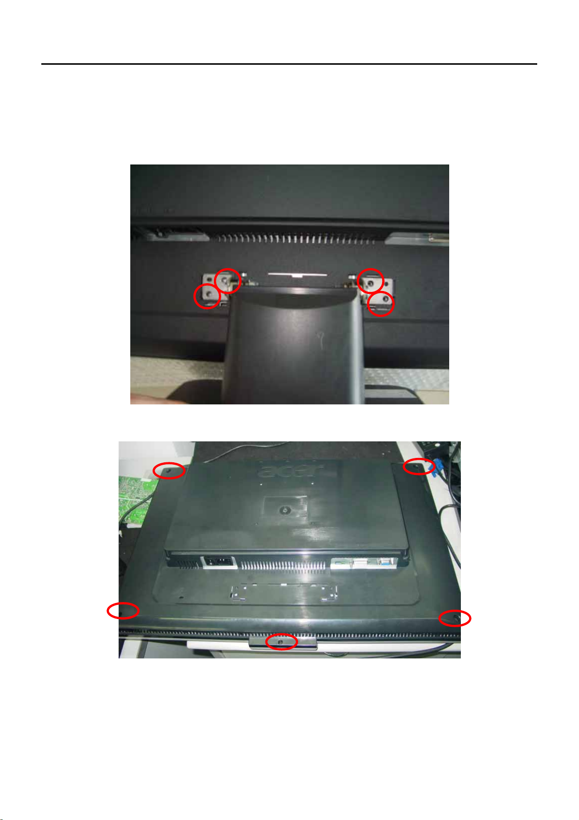
Auto Config
Please Wait
Input Not
Supported
Cable Not
Connected
No Signal
When Analog signal input, if User Press Hot-Key “Auto”, will show this message, and the
monitor do the auto config function.
When the Hsync Frequency, Vsync Frequency or Resolution is out of the monitor
support range, will show this message. This message will be flying.
Analog-Only Model: When the video cable is not connected, will show this message.
This message will be flying.
Analog-Only Model: When the video cable is connected, but there is no active signal
input, will show this message, then enter power saving.
26
Page 27

Logo
When the monitor is power on, the LOGO will be showed in the center, and disappear slowly.
How To Optimize The DOS-Mode
Plug And Play
Plug & Play DDC2B Feature
This monitor is equipped with VESA DDC2B capabilities according to the VESA DDC STANDARD. It allows the
monitor to inform the host system of its identity and, depending on the level of DDC used, communicate additional
information about its display capabilities.
The DDC2B is a bi-directional data channel based on the I²C protocol. The host can request EDID information over
the DDC2B channel.
This monitor will appear to be non-functional if there is no video input signal. In order for this monitor to
operate properly, there must be a video input signal.
This monitor meets the Green monitor standards as set by the Video Electronics Standards Association (VESA)
and/or the United States Environmental Protection Agency (EPA) and The Swedish Confederation Employees
(NUTEK). This feature is designed to conserve electrical energy by reducing power consumption when there is no
video-input signal present. When there is no video input signals this monitor, following a time-out period, will
automatically switch to an OFF mode. This reduces the monitor's internal power supply consumption. After the video
input signal is restored, full power is restored and the display is automatically redrawn. The appearance is similar to
a "Screen Saver" feature except the display is completely off. Pressing a key on the keyboard, or clicking the mouse
restores the display.
Using The Right Power Cord
The accessory power cord for the Northern American region is the wallet plug with NEMA 5-15 style and is UL listed
and CSA labeled. The voltage rating for the power cord shall be 125 volts AC.
Supplied with units intended for connection to power outlet of personal computer: Please use a cord set consisting of
a minimum No. 18 AWG, type SJT or SVT three conductors flexible cord. One end terminates with a grounding type
attachment plug, rated 10A, 250V, and CEE-22 male configuration. The other end terminates with a molded-on type
connector body, rated 10A, 250V, having standard CEE-22 female configuration.
Please note that power supply cord needs to use VDE 0602, 0625, 0821 approval power cord in European counties.
27
Page 28
Machine Disassembly
Chapter 3
This chapter contains step-by-step procedures on how to assemble the monitor for
maintenance.
Disassembly Procedure
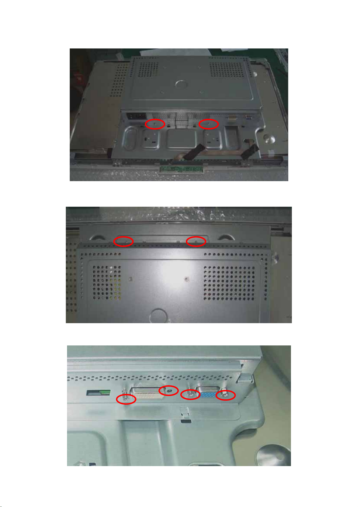
1. Remove the screws to release base stand. (Fig 1)
2. Remove the screws to release back cover. (Fig 2)
Fig 1
Fig 2
28
Page 29
3. Remove the screws to remove the shield. (Fig3- 6)
Fig 3
Fig 4
Fig 5
29
Page 30
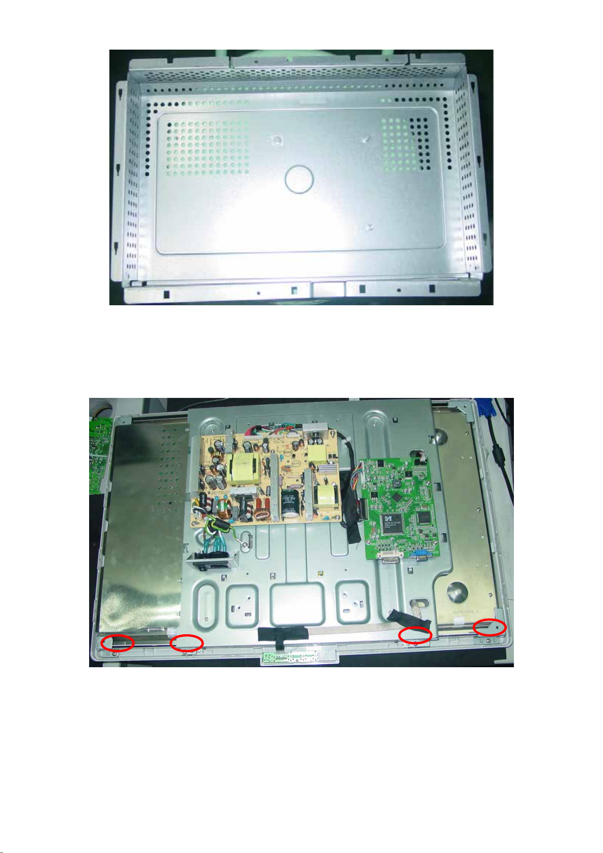
4. Remove the screws to remove the front bezel. (Fig 7-8)
Fig 6
Fig 7
30
Page 31
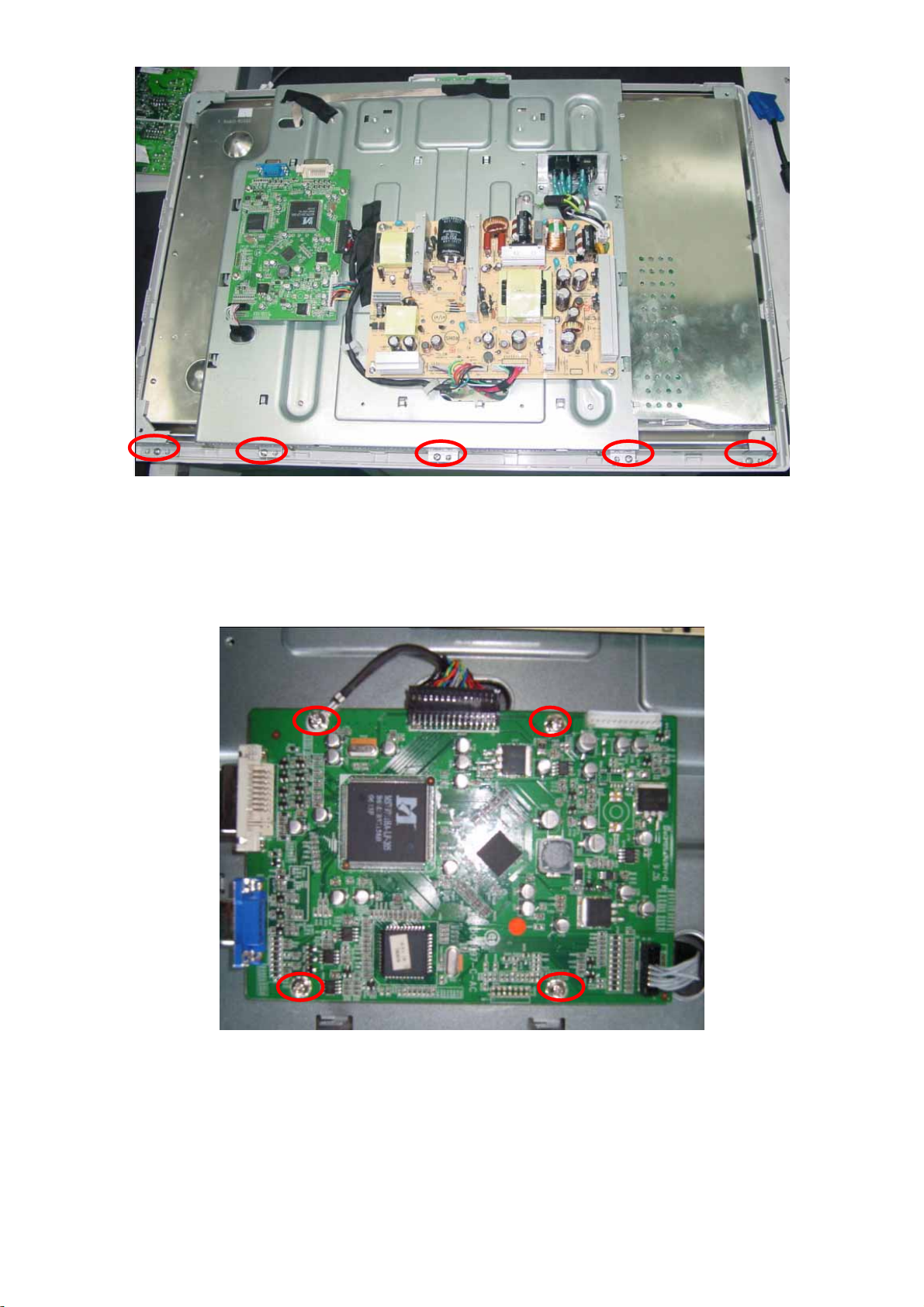
6.
Remove the screws to remove main board.. (Fig 9)
7. Remove the screws to remove power board. (Fig 10)
Fig 8
Fig 9
31
Page 32
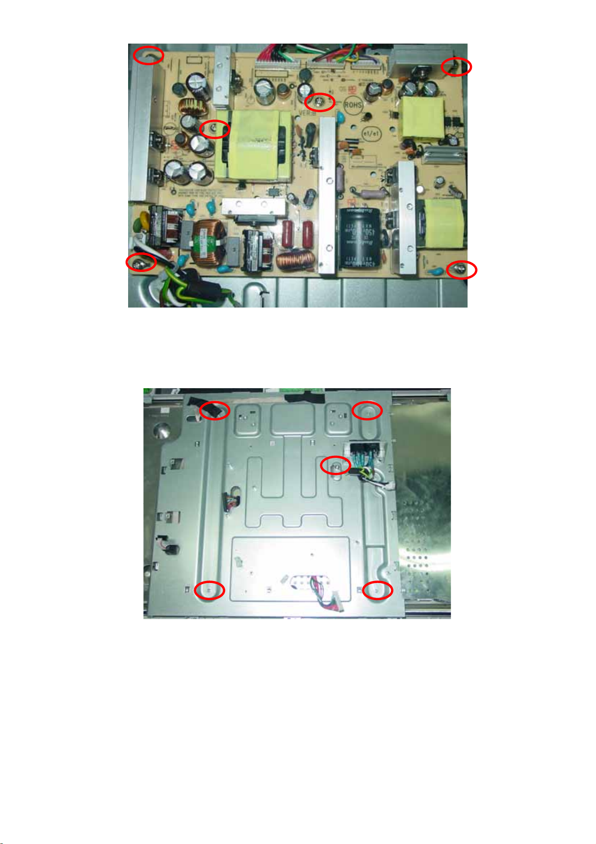
Fig 10
8. Remover the screws connect with panel to remove the main frame and the ground wire. (Fig 11)
9. Remove the screws to remove the main frame. (Fig 12-15)
(Fig 11)
32
Page 33
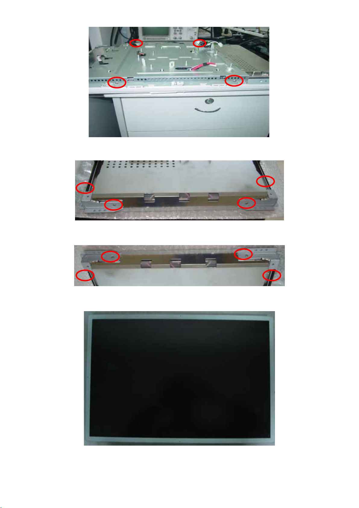
Fig 12
Fig 13
Fig 14
Fig15
33
Page 34
Troubleshooting
Chapter 4
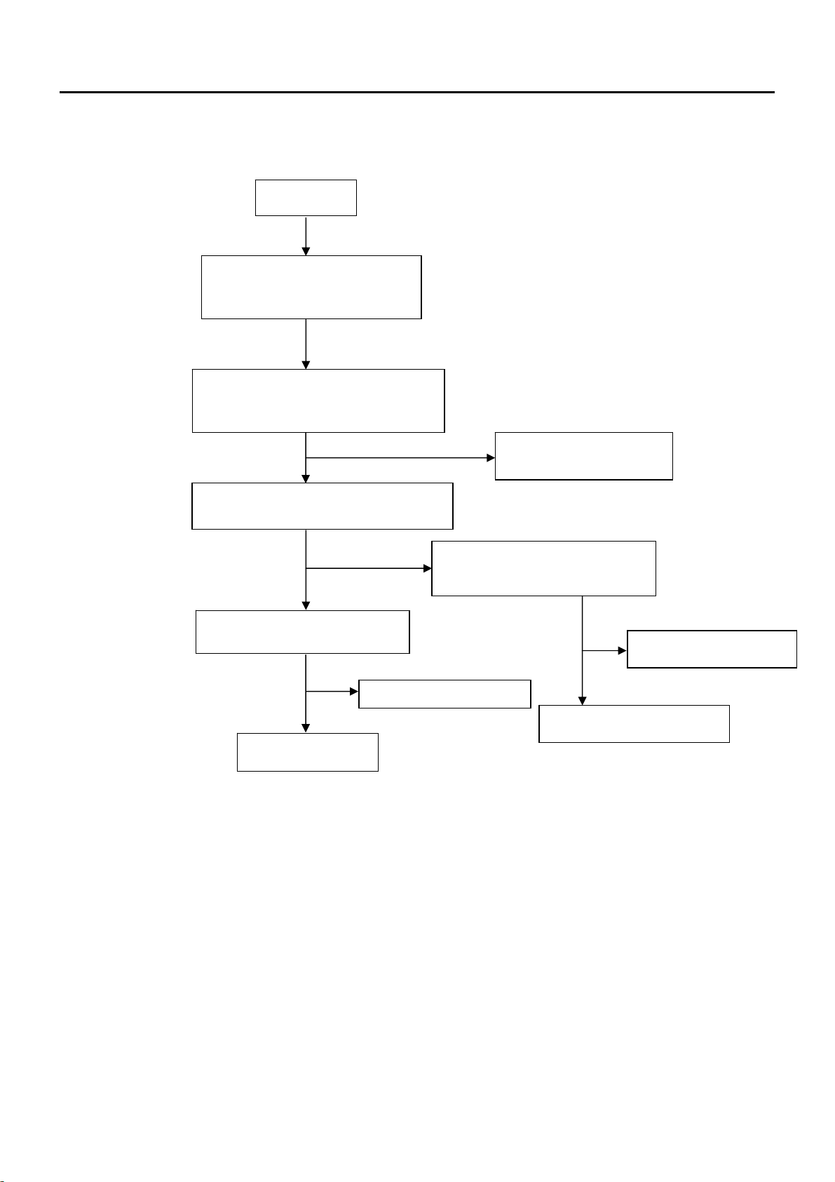
This chapter provides troubleshooting information for the AL2616W:
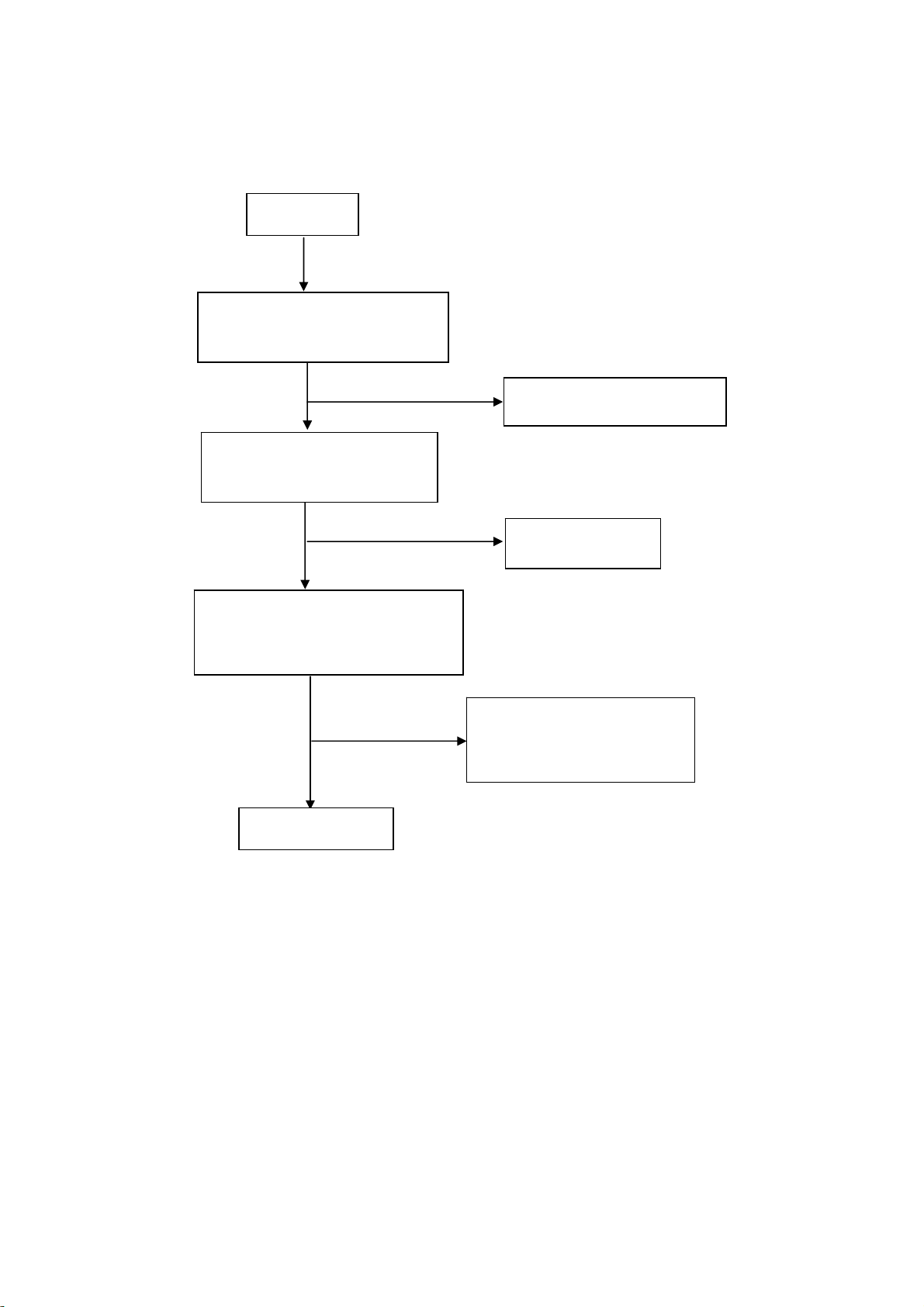
1. No Power
No power
Press power key and look if the
picture is normal
NG
Please reinsert and make sure the
AC of 100-240 is normal
U702 Pin 2=3.3V,U705 Pin 2=3.3V.
OK
Measure U701 Pin 2=3.3V,
NG
Reinsert or check the
power section
OK
Check if X401,X402 oscillate
waveforms are normal
OK
Replace U401
NG
NG
Replace X401,X402
Meas
r
Replace Power section
Replace U701,U703,U705
34
Page 35
2. No Picture
No picture
Measure U701 PIN2=3.3V
U702 PIN2=3.3V,U705 PIN2=3.3
OK
Check if X401,X402 oscillate
waveforms are nor
OK
Check if the sync signal from
computer is output and video cable
is connected normally
OK
NG
NG
NG
Replace U701, U702, U705
Replace X401,
X402
Input the sync signal of
computer, or change the
cable
Replace U401
35
Page 36
3. Panel Power Circuit
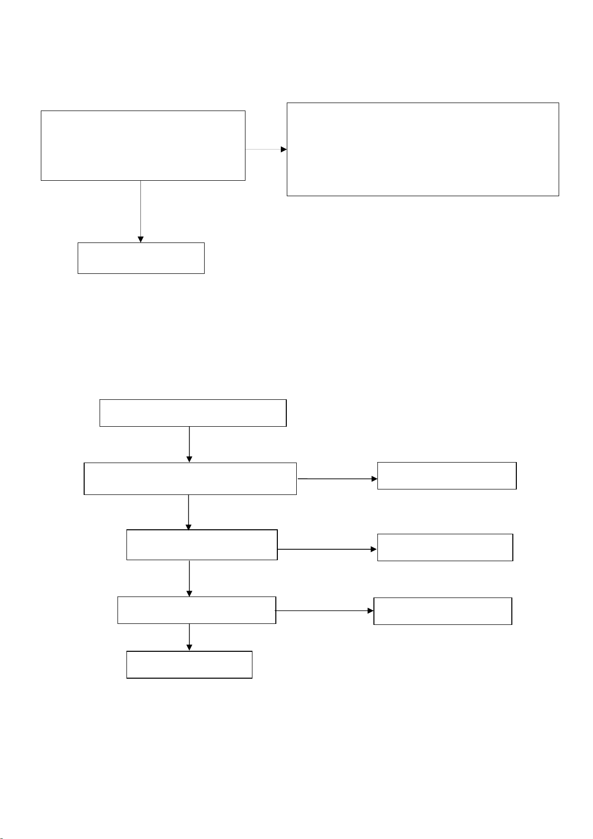
Check CN407 PIN 23-24 should have
response from 0V to 5V When we
switch the power switch from on to off
OK
Replace panel
4. Keypad Board
OSD is unstable or not working
Is Keypad board connecting normally?
OK
Is Button Switch normally?
OK
Is Keypad board normally?
OK
Check main board
Check the PPWR panel power relative circuit,Q702, Q705
NG
Q703 In normal operation, when LED =green, R706
Should =5 V,
If PPWR no-response when the power switch
Turn on and turn off, replace the U401-MST9251A
NG
Connect Keypad Board
NG
Replace Button Switch
NG
Replace Keypad Board
36
Page 37
5. PWPC
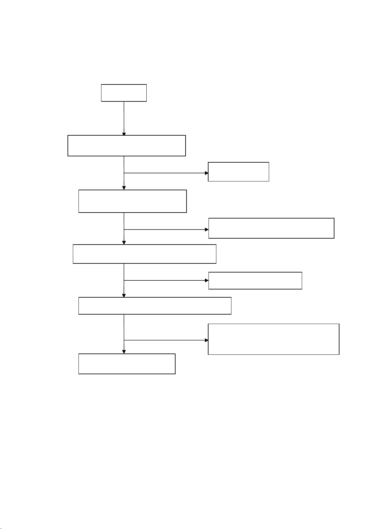
No Power
No power
Check AC line volt 110V or 220V
OK
Check the voltage of C907(+)
OK
Check start voltage for the pin3 of IC901
OK
Check the auxiliary voltage is between 10V-16V
OK
NG
NG
NG
NG
Check AC line
Check F901, bridge rectified circuit
Check R912,R931,IC901
Check IC901,T901,T902
Check ZD903, ZD905
Check ZD909, ZD910, IC902
37
Page 38
6. No Backlight
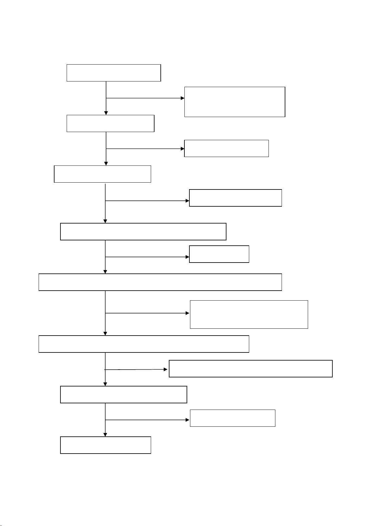
Check C801 (+) =12V
OK
NG
Check ON/OFF signal
NG
OK
Check IC801 pin9=12V ?
NG
OK
Check the pin1 of IC201 have saw tooth wave
NG
OK
Check D801 (-) has the output of square wave at short time.
Change F901
Check Q803
Check Interface board
Change Q801 or Q802
Change IC801
NG
OK
Check the resonant wave of pin2 & pin5 for PT801/ PT802
OK
NG
Check the output of PT801/PT802
NG
OK
Check connecter & lamp
Check Q806/Q807/C841
CheckQ805/Q807/Q803/Q801or
/Q806/Q808/Q804/D802
Change PT801/PT802
38
Page 39
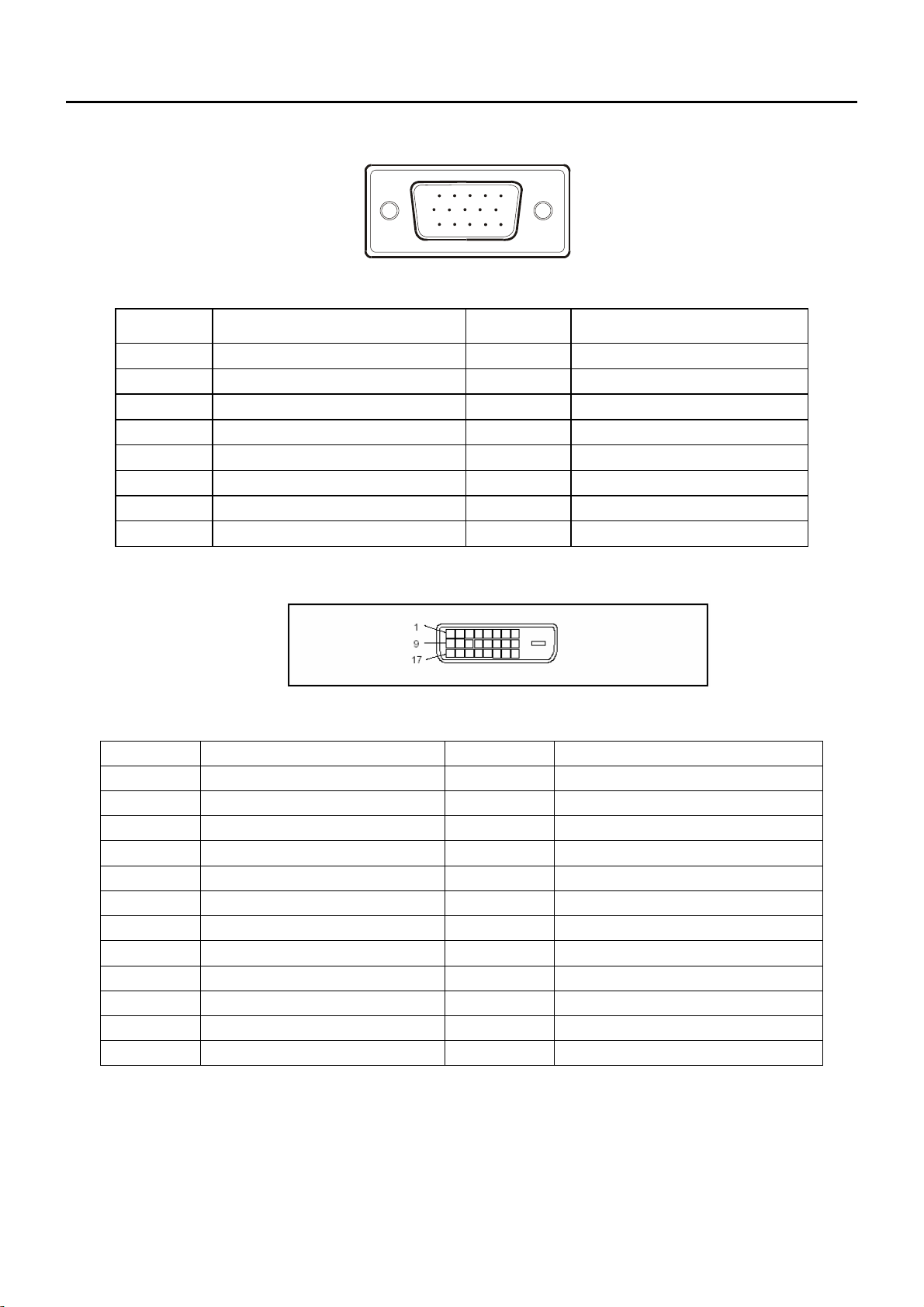
Connector Information
Chapter 5
The following figure shows the connector locations on the monitor:
15
6
11 15
10
15 – Pin Color Display Signal Cable (D-sub)
Pin No. Description Pin No. Description
1. Red 9. +5V
2. Green 10. Logic Ground
3. Blue 11. Monitor Ground
4. Monitor Ground 12. DDC-Serial Data
5. DDC-Return 13. H-Sync
6. R-Ground 14. V-Sync
7. G-Ground 15. DDC-Serial Clock
8. B-Ground
24 – Pin Color Display Signal Cable (DVI)
Pin No. Description Pin No. Description
1. TMDS Data2- 13. TMDS Data3+
2. TMDS Data2+ 14. +5V Power
3. TMDS Data 2/4 Shield 15. GND
4. TMDS Data4- 16. Hot Plug Detect
5. TMDS Data4+ 17. TMDS Data0-
6. DDC Clock 18. TMDS Data0+
7. DDC Data 19. TMDS Data 0/5 Shield
8. Analogue Vertical Sync 20. TMDS Data5-
9. TMDS Data1- 21. TMDS Data5+
10. TMDS Data1+ 22. DDC Clock Shield
11. TMDS Data 1/3 Shield 23. DDC Clock+
12. TMDS Data3- 24. DDC TMDS Clock-
39
Page 40

FRU (Field Replaceable Unit) List
This chapter gives you the FRU (Field Replaceable Unit) listing in global configurations of AL2616W.Refer to this
chapter whenever ordering for parts to repair or for RMA (Return Merchandise Authorization).
NOTE: Please note WHEN ORDERING FRU PARTS, that you should check the most up-to-date information
available on your regional web or channel (http://aicsl.acer.com.tw/spl/). For whatever reasons a part number
change is made, it will not be noted in the printed Service Guide. For ACER AUTHORIZED SERVICE
PROVIDERS, your Acer office may have a DIFFERENT part number code from those given in the FRU list of
this printed Service Guide. You MUST use the local FRU list provided by your regional Acer office to order
FRU parts for repair and service of customer machines.
NOTE: To scrap or to return the defective parts, you should follow the local government ordinance or regulations on
how to dispose it properly, or follow the rules set by your regional Acer office on how to return it.
Chapter 6
40
Page 41
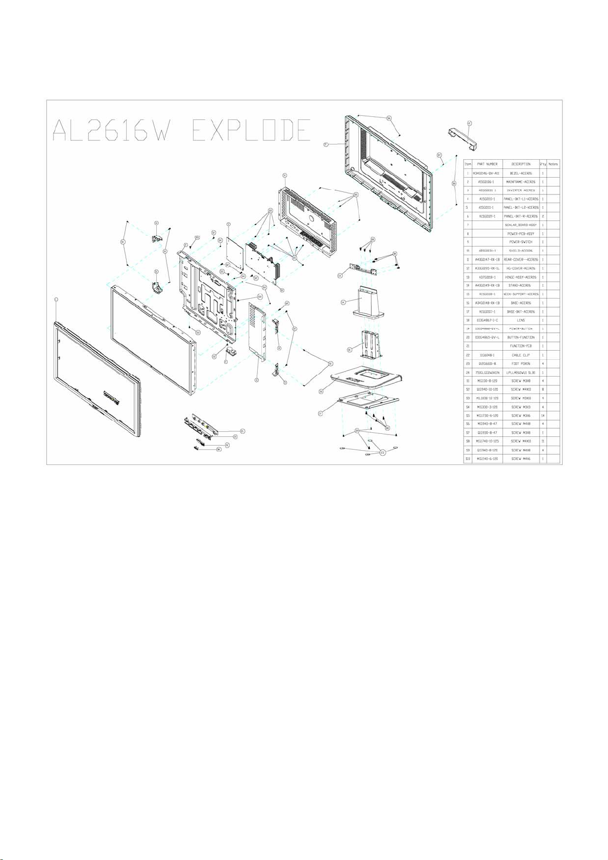
Exploded Diagram (Model: AL2616W)
41
Page 42
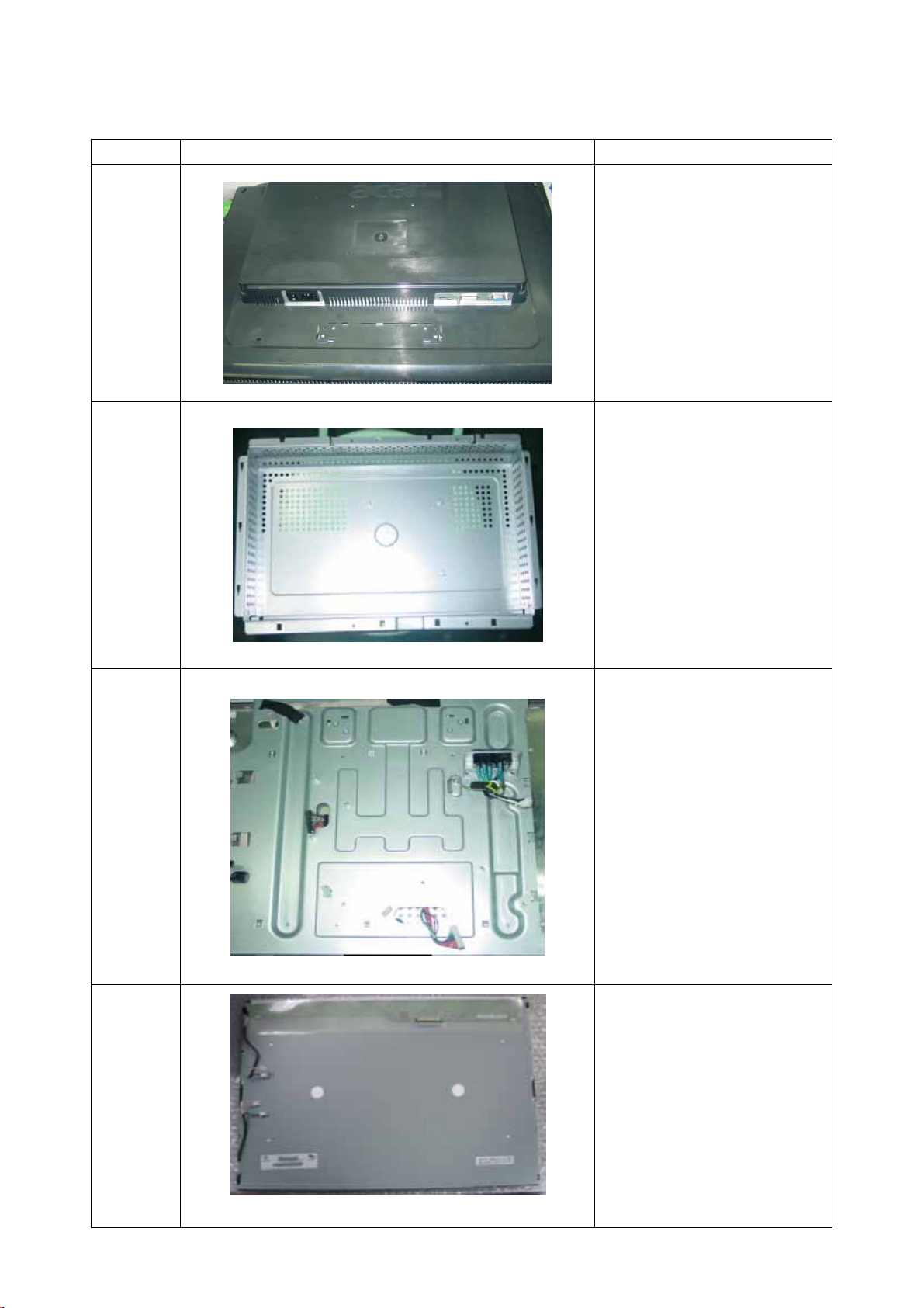
Part List
Above picture show the description of the following component.
Item Picture Description
1
2
Back Cover
Shield
3
4
42
Main Frame
Panel
Page 43
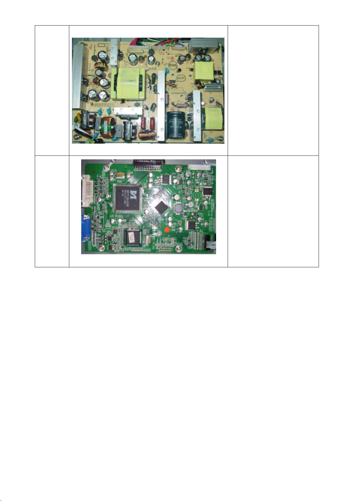
5
Power Board
6
Main Board
43
Page 44
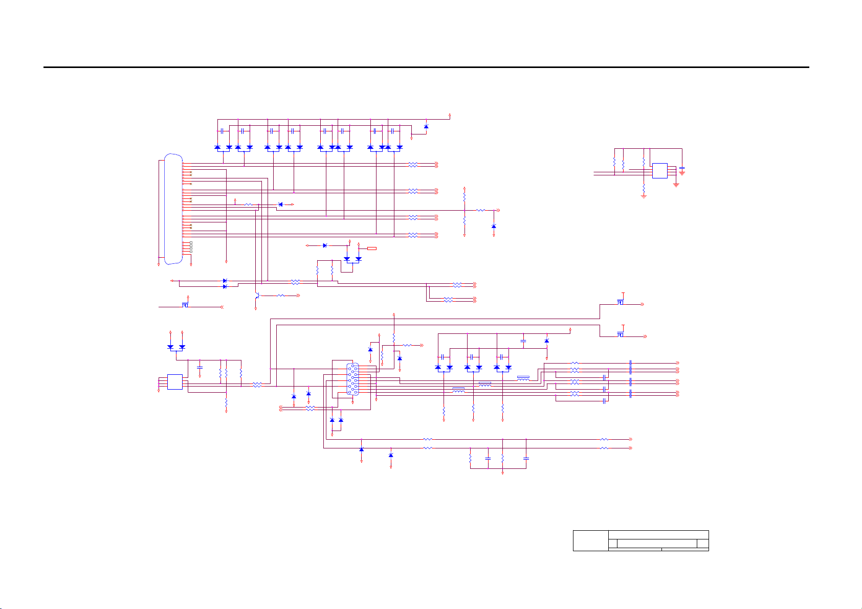
Schematic Diagram
Chapter 7
Main Board
Graphics/ Components In
DVI CONNECTOR
31
32
GND
EDID_WP
GND
ANALOG DDC
CN102
31
RX2+
GND
RX4RX4+
RX1RX1+
GND
RX3RX3+
GND
RX0RX0+
GND
RX5RX5+
GND
RXC+
RXC-
RED
GRN
GND
32
JACK
GND
VGA_5V
1
U101
1
A0
VCC
2
A1
3
A2
4 5
VSS SDA
C120
0.1uF
1
2
D107
3
DVISCL
DVISDA
RX1-IN
RX1+IN
R136
10K 1/10W
HOT_PLUG
RX0-IN
RX0+IN
RXC+IN
RXC-IN
PMBS3904
GND
R122
10K 1/10W
R120 100 1/10W
R121 100 1/10W
C116
0.1uF
2
D108
BAV99
3
ZD118 UDZS5.6B
DVISCL
DVISDA
Q105
UDZS5.6B
RXD4
TXD4
1
BAV99
R124 100 1/10W
R125 100 1/10W
R186
4.7K 1/10W
VGASCL
ZD107
GND
C115
0.1uF
1
2
D106
BAV99
BAV99
3
RX2-IN
1
RX2-
SCL
SDA
BLU
3
SCL
RX2+IN
2
3
4
5
6
7
8
VS
9
10
11
12
13
14
5V
15
16
HP
17
18
19
20
21
22
23
24
C1
25
C2
26
C3
27
C4
28
HS
C5
29
GND
+5V
G
1
2
WP_DDC
3
Q101
D
S
2N7002
+5V
2
D104
BAV70
C113
1uF
8
GND
7
WP
6
EDID_WP
DVI_HPD
VGA_EDID
10K 1/10W
ZD108 UDZS5.6B
R123
DVI_5V
GND
ZD109 UDZS5.6B
WP_DDC 4
R150
NC
R151
0 1/10W
GND
C121
2
12
D109
VGASDA
0.1uF
3
GND
1
GND
10K 1/10W
HPD_CTRL 4
GND
C117
BAV99
ZD111
R126
VGA_SCL_IN
VGA_SDA_IN
ZD106
UDZS5.6B
R118
NC
R119
NC
2
D110
UDZS5.6B
DVI_EDID
C118
C122
0.1uF
0.1uF
1
1
2
D111
BAV99
3
3
DVI_5V
1
3
R127
10K 1/10W
CN101
15
14
13
12
11
17 16
GND
ZD103
ZD102
UDZS5.6B
UDZS5.6B
A-HS
GND
A-VS
+5V
2
UDZS5.6B
DB26
10
5
9
4
8
3
7
2
6
1
GND
C123
0.1uF
0.1uF
1
2
1
2
GND
A-BLUE
A-GREEN
A-RED
BAV99
R183
NC
D113
3
+5V
GND
GND
R137 10 1/10W
R138 10 1/10W
R139 10 1/10W
R140 10 1/10W
R141 10 1/10W
R142 10 1/10W
R143 10 1/10W
R144 10 1/10W
10K 1/10W
R181
R182100 1/10W
ZD117
UDZS5.6B
GND
ZD105
UDZS5.6B
D112
BAV99
3
+5V 4,6
BAV70
D105
VGA_5V
ZD101
GND
GND
ZD104
UDZS5.6B
+5V
ZD112
UDZS5.6B
RX2- 5
RX2+ 5
RX1- 5
RX1+ 5
RX0- 5
RX0+ 5
RXC+ 5
RXC- 5
R164 100 1/10W
R165
100 1/10W
R184 100 1/10W
R185 100 1/10W
C124
0.1uF
1
2
D102
BAV99
3
L101 0 OHM
R108
75 1/10W
GND
R112
2.2K 1/10W
+5V
R149
10K 1/10W
R145
R146
100 1/10W
100K 1/10W
GND
DVI_SCL 5
DVI_SDA 5
SDA_D1 4
SCL_D1 4
C125
0.1uF
1
2
3
L102 0 1/10W
R109
75 1/10W
GND
DVI Test Points are just SMTobservation points
on the traces with no stub
SCL_D
SDA_D
VGA_CAB 4
D101
BAV99
R460 100 1/10W
R111 100 1/10W
D103
BAV99
UDZS5.6B
GND
C111
220pF
DVI_CAB 4
ZD110
C126
0.1uF
2
L103
3
R110
75 1/10W
GND
R113
2.2K 1/10W
GND
DVI_EDID
+5V
1
G
Q104
2N7002
+5V
1
G
Q103
2N7002
C104 0.001uF
C103 0.047uF
C107 0.047uF
C102 0.047uF
C106 0.047uF
C101 0.047uF
C105 0.047uF
R169
10K 1/10W
EDID_WP
2
S
2
S
C101-107 47 nf
R170
NC
R171
NC
VGA_SCL 4
AHS0 5
AVS0 5
U102
8
VCC
7
WP
6
SCL
VSSSDA
DDC_D
VGA_SDA 4
1
A0
C140
2
A1
3
1uF
A2
45
SOG0 5
BLUE0+ 5
BLUE0- 5
GREEN0+ 5
GREEN0- 5
RED0+ 5
RED0- 5
R168
10K 1/10W
SCL_D
SDA_D
3
D
+5V
C108 5pF
C109 5pF
C110 5pF
R114 150 1/10W
R115 1K 1/10W
3
D
C119
1uF
ZD113
UDZS5.6B
1
C112
47pF
0 1/10W
GND
R104 470 1/10W
R103 56 1/10W
R107 100 1/10W
R102 56 1/10W
R106 100 1/10W
R101 56 1/10W
R105 100 1/10W
Title
MST9251A/HA
Size Document Number Rev
C
02. Graphics/Components in
Date: Sheet
44
B
26Monday, June 19, 2006
of
Page 45
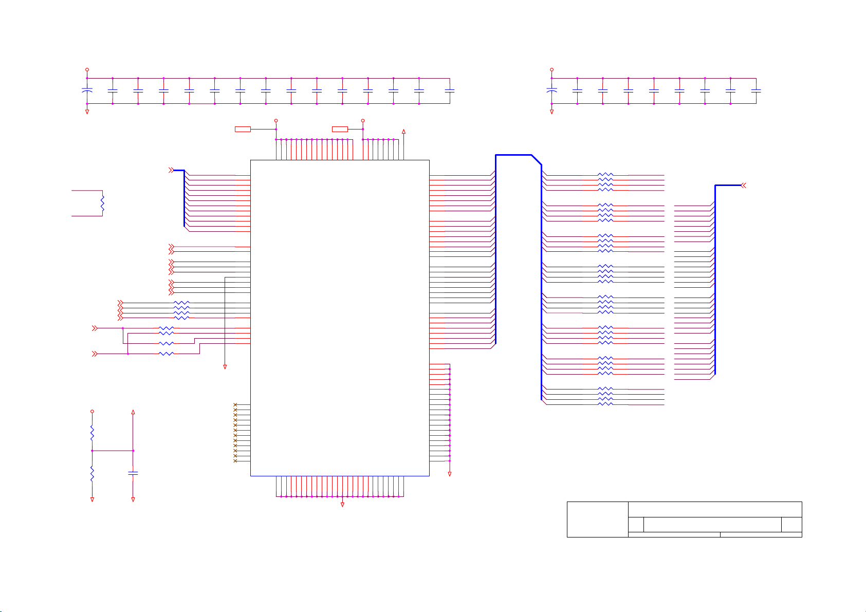
Frame Memory
+2.5V_DMQ
+2.5V_DMC
C302
0.1uF
FSADDR[0..11]5
FSVREF
GND
C316
0.1uF
C303
0.1uF
FSBKSEL05
FSBKSEL15
FSCLK-5
FSCLK+5
FSCKE5
/FSRAS5
/FSCAS5
/FSWE5
C301
+
22uF/16V
GND
FSCLK+
R311
+2.5V_DMQ
GND
150 1/10W
FSDQSU05
FSDQSU25
FSDQSU15
FSDQSU35
FSDQM0
FSDQM1
R309
10K 1/10W
FSVREF
R310
10K 1/10W
FSCLK-
Place this parallel termination close to
corresponding memory IC Pins
FSDQM05
FSDQM15
Near The DDR-SDRAM IC
C305
C304
0.1uF
0.1uF
FSADDR0
FSADDR1
FSADDR2
FSADDR3
FSADDR4
FSADDR5
FSADDR6
FSADDR7
FSADDR8
FSADDR9
FSADDR10
FSADDR11
FSBKSEL0
FSBKSEL1
FSCLKFSCLK+
FSCKE
/FSRAS
/FSCAS
/FSWE
R301 0 1/10W
R302 0 1/10W
R303 0 1/10W
0FSDQS2
R304 0 1/10W
R305 100 1/10W
R306 100 1/10W
R307 100 1/10W
R308 100 1/10W
Near The
DDR-SDRAM IC
Stub as short as
possible.
C306
0.1uF
+2.5V_DMQ6
FSDQS3
FSDQS1
FSDQS0
FSDQM11
FSDQM01
FSDQM00
FSDQM10
GND
C307
0.1uF
+2.5V_DMQ
U303
M4
A0
M5
A1
L5
A2
M6
A3
M7
A4
L8
A5
M8
A6
M9
A7
M10
A8/AP
L7
A9
K5
A10
L6
A11
M3
BA0
L4
BA1
L11
CK#
L10
CK
M11
CKE
M1
CS#
L1
RAS#
K1
CAS#
K2
WE#
A1
DQS0
G12
DQS1
G1
DQS2
A12
DQS3
A2
DM0
G11
DM1
G2
DM2
A11
DM3
B3
NC
B10
NC
G3
NC
G10
NC
K8
NC
K11
NC
K12
NC
L2
NC
L3
NC
L9
NC
L12
NC
M2
NC
EM6A9320BI-5M
C310
0.1uF
VDDQ
VSS
VDDQ
VDDQ
VSS
VSS
VDDQ
VSS
GND
VDDQ
VSS
C311
0.1uF
+2.5V_DMC
VDDQ
VDDQ
VDDQ
VSS
VSS
VSS
C6C7D3
VDD
VSS
VSS
C312
0.1uF
D10K3K6K7K10
VDD
VDD
VDD
VSS
VSS
VSS
VDD
VSS
C309
C308
0.1uF
0.1uF
+2.5V_DMC6
B2B4B6B7B9
B11D2D11E3E10F3F10H3H10J3J10
VDDQ
VDDQ
VDDQ
VDDQ
VDDQ
VDDQ
VDDQ
VDDQ
VSS
VSS
VSS
VSS
VSS
VSS
VSS
VSS
D4D6D7D9E5E6E7E8F5F6F7F8G5G6G7G8H5H6H7H8J5J6J7J8K4
VDD
VSS
C313
0.1uF
FSVREF
VDD
VDD
VSS
VSS
M12
K9
VREF
VSS
DQ0
DQ1
DQ2
DQ3
DQ4
DQ5
DQ6
DQ7
DQ8
DQ9
DQ10
DQ11
DQ12
DQ13
DQ14
DQ15
DQ16
DQ17
DQ18
DQ19
DQ20
DQ21
DQ22
DQ23
DQ24
DQ25
DQ26
DQ27
DQ28
DQ29
DQ30
DQ31
VSSQ
VSSQ
VSSQ
VSSQ
VSSQ
VSSQ
VSSQ
VSSQ
VSSQ
VSSQ
VSSQ
VSSQ
VSSQ
VSSQ
VSSQ
VSSQ
VSSQ
VSSQ
VSSQ
VSSQ
C314
0.1uF
A6
B5
A5
A4
B1
C2
C1
D1
J12
J11
H12
H11
F12
F11
E12
E11
E2
E1
F2
F1
H2
H1
J1
J2
D12
C12
C11
B12
A9
A8
B8
A7
A3
A10
C3
C4
C5
C8
C9
C10
D5
D8
E4
E9
F4
F9
G4
G9
H4
H9
J4
J9
GND
C315
0.1uF
FSDATA0
FSDATA1
FSDATA2
FSDATA3
FSDATA4
FSDATA5
FSDATA6
FSDATA7
FSDATA16
FSDATA17
FSDATA18
FSDATA19
FSDATA20
FSDATA21
FSDATA22
FSDATA23
FSDATA8
FSDATA9
FSDATA10
FSDATA11
FSDATA12
FSDATA13
FSDATA14
FSDATA15
FSDATA24
FSDATA25
FSDATA26
FSDATA27
FSDATA28
FSDATA29
FSDATA30
FSDATA31
FSDATA[0..31]
2
1
3
C317
C318
+
22uF/16V
0.1uF
GND
RN301
FSDATA0
FSDATA1
FSDATA2
FSDATA3
FSDATA4
FSDATA5
FSDATA6
FSDATA7
FSDATA20
FSDATA21
FSDATA22
FSDATA23
8
7
6
5
RN302 100 1/16W
8
7
6
5
RN303
8
7
6
5
RN304
8
7
6
5
RN305
8
7
6
5
RN306
8
7
6
5
RN307
8
7
6
5
RN308
8
7
6
5
FSDATA24
FSDATA25
FSDATA26
FSDATA27
FSDATA28
FSDATA29
FSDATA30
FSDATA31
FSDATA8
FSDATA9
FSDATA10
FSDATA11
FSDATA12
FSDATA13
FSDATA14
FSDATA15
FSDATA16
FSDATA17
FSDATA18
FSDATA19
Near The DDR-SDRAM IC
C321
0.1uF
C322
0.1uF
FSDATAU0
FSDATAU1
FSDATAU2
FSDATAU3
FSDATAU4
FSDATAU5
FSDATAU6
FSDATAU7
FSDATAU8
FSDATAU9
FSDATAU10
FSDATAU11
FSDATAU12
FSDATAU13
FSDATAU14
FSDATAU15
FSDATAU16
FSDATAU17
FSDATAU18
FSDATAU19
FSDATAU20
FSDATAU21
FSDATAU22
FSDATAU23
FSDATAU24
FSDATAU25
FSDATAU26
FSDATAU27
FSDATAU28
FSDATAU29
FSDATAU30
FSDATAU31
C320
C319
0.1uF
0.1uF
100 1/16W
FSDATAU24
1
2
FSDATAU25
3
FSDATAU26
4
FSDATAU27
1
FSDATAU28
FSDATAU29
2
FSDATAU30
3
4
FSDATAU31
100 1/16W
FSDATAU8
1
FSDATAU9
2
FSDATAU10
3
FSDATAU11
4
100 1/16W
1
FSDATAU12
FSDATAU13
2
3
FSDATAU14
FSDATAU15
4
100 1/16W
FSDATAU0
1
FSDATAU1
2
FSDATAU2
3
FSDATAU3
4
100 1/16W
FSDATAU4
1
FSDATAU5
2
FSDATAU6
3
FSDATAU7
4
100 1/16W
1
FSDATAU16
FSDATAU17
2
FSDATAU18
3
FSDATAU19
4
100 1/16W
FSDATAU20
1
FSDATAU21
2
3
FSDATAU22
FSDATAU23
4
Title
MST9251A/HA
Size Document Number Rev
B
03. Frame Memory
Date: Sheet
0.1uF
C324
0.1uF
C323
C325
0.1uF
FSDATAU[0..31] 5
of
36Monday, June 19, 2006
D
45
Page 46
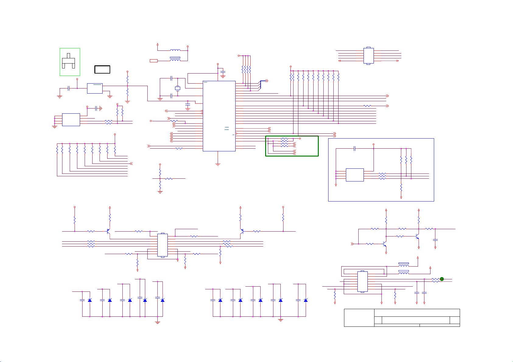
MCU
3
VCC
LM810M3-2.93V
DIO/MA730
1
GND
C429
0.1uF
U403
1
A0
2
A1
3
A2
4 5
VSS SI
M24C16
R450
R451
R463
10K 1/10W
10K 1/10W
R417
4.7K 1/10W
LED_G
KEY_AUTO
KEY_DOWN
KEY_ONOFF
2
RESET
VMCU
12
3
MAX810STR
VMCU
8
VCC
7
WP
6
SCK
R452
R453
1K 1/10W
10K 1/10W
VMCU
1K 1/10W
R418
R424 220 1/10W
R426 220 1/10W
R428 220 1/10W
MODE_VOLUME-1
C432
NC
RESET IC
ACTIVE HIGH /RESET
U404
RESET
Vcc
GND
C430
1uF
WP
R454
R455
10K 1/10W
10K 1/10W
100 1/10W
PMBS3906
LED_GREEN
C433
NC
0.1uF
ZD401
2
1
VMCU
R408
4.7K 1/10W
R410 100 1/10W
R411 100 1/10W
VMCU
R456
R457
10K 1/10W
VGA_CAB
10K 1/10W
DVI_CAB
10K 1/10W
AUDIO_MUTE
PS_ON
HWRESET
ALE
ON_PANEL
ON_PBACK
KEY_MUTE
+3.3V_VDD
R419
Q402
MODE_VOLUME-
LED_GREEN
KEY_AUTO1
KEY_DOWN1
KEY_ONOFF1
SPKR_L-
C434
0.1uF
ZD402
UDZS5.6B
VMCU
R468
NC
R409
4.7K 1/10W
MSCL
MSDA
NC
R464
KEY_AUTO1
ZD403
R401
100K 1/10W
VBR_OUT5
PS_ON 6
R448
NC
SPKR_L+
R465
NC
GND
KEY_DOWN1
C435
0.1uF
UDZS5.6B
+5V_PANEL
+3.3V_VDD6
POWER FOR MCU
RESET
VMCU
KEY_DOWN1
WP
R416
NC
MODE_VOLUME-1
1
3
5
7
9
11
13
15
KEY_ONOFF1
C436
0.1uF
ZD404
UDZS5.6B
INT5
VGA_CAB2
ON_DDR2
DVI_CAB2
HWRESET5
ON_PANEL6
ON_PBACK6
KEY_MUTE
VMCU
R414
10K 1/10W
CONN
CN401
ZD405
L401
NC
L405
120 OHM
C401 22pF
C402 22pF
INT
VGA_CAB
R 10K 1/
443 10W
DVI_CAB
AUDIO_MUTE
PS_ON
HWRESET
ALE
ALE5
ON_PANEL
ON_PBACK
R449 220 1/10W
R415
WP_MCU
100 1/10W
SOURCE_VOLUME+1
2
4
6
8
10
12
14
16
GND
UDZS5.6B
VMCU
X40124.576MHz
C406
0.1uF
MSCL
MSDA
220 1/10W
R423
SPKR_R+
GND
EA/VP
UCLK
R466
R467
NC
For Bank Select
Syntek 128kB
Issue
VMCU
U402
35
EA/VP
21
X1
20
X2
10
RESET
14
INT0/P3.2
15
INT1/P3.3
16
T0/P3.4
17
T1/P3.5
36
P0.7
37
P0.6
38
P0.5
39
P0.4
40
P0.3
41
P0.2
42
P0.1
43
P0.0
1
P4.2
12
P4.3/ISP
GND VCC
MTV416
22 44
AUDIO_STDBY
KEY_MENU1
KEY_MUTE1
NC
KEY_UP1
SPKR_R-
KEY_MUTE1
C404
NC
R425 220 1/10W
R427 220 1/10W
GND
ZD410
VMCU
C403
0.1uF
P1.0
P1.1
P1.2
P1.3
P1.4
P1.5
P1.6
P1.7
P2.0
P2.1
P2.2
P2.3
P2.4
P2.5
P2.6
P2.7
RD/P3.7
WR/P3.6
PSEN
ALE/P
TXD/P3.1
RXD/P3.0
P4.0
P4.1
LED_ORANGE
R462
NC
R482
0 1/10W
KEY_UP1
C437
NC
0.1uF
123
876
2
3
4
5
6
7
8
9
24
25
26
27
28
29
30
31
19
18
32
33
13
11
23
34
+3.3V_VDD
ZD406
4
5
LED_O
LED_G
R422
100 1/10W
Q403
PMBS3906
KEY_MENU
KEY_UP
KEY_MUTE
KEY_MENU1
C438
0.1uF
UDZS5.6B
RN401
10K 1/16W
AD0
AD1
AD2
AD3
R421
ZD407
1K 1/10W
R444
AD[0..3] 5
HDCP_WP
SCL_D1 2
SDA_D1 2
R406100 1/10W
R407100 1/10W
Near the VGA Connector.
(ISP & DDC-CI)
VMCU
R420
4.7K 1/10W
LED_O
LED_ORANGE
C439
0.1uF
ZD408
UDZS5.6B
UDZS5.6B
VMCU
R403
R402
10K 1/10W
4.7K 1/10W
R4044.7K 1/10W
R4054.7K 1/10W
VGA_SDA 2
VGA_SCL 2
RXD
RXD 2
TXD
TXD 2
SOURCE_VOLUME+1
C405
0.1uF
R473
4.7K 1/10W
VMCU
R474
10K 1/10W
KeyPad connector
CN403
2
KEY_AUTO1
U405
1
A0
2
A1A2WP
3
4
GND
M24C04-WMN6T
1
3
5
7
9
R442 220 1/10W
KEY_ONOFF
KEY_MENU
KEY_DOWN
KEY_UP
KEY_AUTO
AUDIO_STDBY
WP_MCU
C440
1uF
VCC
SCL
SDA
CONN
MODE_VOLUMEHDCP_SCL
HDCP_SDA
VMCU
8
R484 100 1/10W
7
R485 100 1/10W
6
R486 100 1/10W
5
4
6
8
10
LED_GREEN
KEY_ONOFF1
KEY_DOWN1
GND
R478
R476
R477
R475
10K 1/10W
R479
R480
10K 1/10W
RD
WR
10K 1/10W
10K 1/10W
10K 1/10W
10K 1/10W
10K 1/10W
RD 5
WR 5
GND
For AOC
LED_ORANGE
KEY_MENU1
KEY_UP1
SOURCE_VOLUME+1
HPD_CTRL 2
WP_DDC 2
R490
NC
GND
R489 10K 1/10W
R487 4.7K 1/10W
R488 4.7K 1/10W
HDCP_WP
HDCP_SCL
HDCP_SDA
For HDCP
GND
+5V
R472
1K 1/10W
R491 NC
1
3
5
7
9
11
13
R441
4.7K 1/10W
CN402
2
4
6
8
10
12
14
NC
Title
Size Document Number Rev
Date: Sheet
VOL_PWM5
VOL
SPKR_L+
SPKR_L-
R469
NC
ZD409
UDZS5.6B
GND
R471 NC
R429
4.7K 1/10W
Q405
PMBS3904
GND
1 2
1 2
STANDBY
SPKR_R+
SPKR_R-
GND
GND
MST9251A/HA
A3
04. MCU
L402 600 OHM
L403
600 OHM
MUTE
R470
NC
+5V
GND
+12V
GND
Q404
PMBS3904
R430
1K 1/10W
R431 0 1/10W
+5V
R432 0 1/10W
R433
0 1/10W
C417
C416
NC
NC
GND
VOL
C414NC
GND
AUDIO_STDBY
AUDIO_MUTE
B
46Monday, June 19, 2006
of
46
Page 47
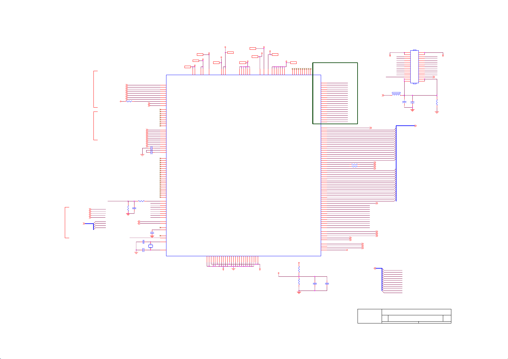
MST9251A
MCU INTERFACE
+3.3DV1
AVDD_PLL6
+3.3DV1 6
+APLL6
+2.5MVDD6
86
102
162
182
VDDP
VDDP
VDDP
VDDM
MST9251A(208Pin)
GND
GND
GND
GND
GND
GND
GND
GND
GND
GND
80
15764183
132
155
87
108
140
103
114
126
AVDDA
VDD_MPLL
+3.3DV2
AVDD_DVI
+3.3DV26
10
34
204
4
AVDD_DVI
AVDD_ADC
AVDD_ADC
66
AVDD_DVI
AVDD_MPLL
GND
GND
GND
GND
GND
GND
GND
1
16
351250
7
13
65
GND
VDD_MPLL6
AVDD_DVI6
AVDDA6
U401
RX2+
C427 0.1uF
C428
ADJ_PWM
14.318MHz
C41947pF
RX2RX1+
RX1RX0+
RX0RXC+
RXC-
207
DVI_R+
208
DVI_R-
2
DVI_G+
3
DVI_G-
5
DVI_B+
6
DVI_B-
8
DVI_CK+
9
DVI_CK-
11
REXT
14
DDCD_DA
15
DDCD_CK
18
HSYNC1
19
VSYNC1
20
BIN1
21
BIN1M
22
SOGIN1
23
GIN1
24
GIN1M
25
RIN1
26
RIN1M
27
BIN0M
28
BIN0
29
GIN0M
30
GIN0
31
SOGIN0
32
RIN0M
33
RIN0
36
HSYNC0
37
VSYNC0
38
RMID
39
REFP
40
REFM
0.1uF
41
VI_DATA[8]
42
VI_DATA[9]
43
VI_DATA[10]
44
VI_DATA[11]
45
VI_DATA[12]
46
VI_DATA[13]
47
VI_DATA[14]
48
VI_DATA[15]
51
GPIO[5]/VHS
52
GPIO[4]/VCLK2
53
VI_CK
54
VI_DATA[0]
55
VI_DATA[1]
56
VI_DATA[2]
57
VI_DATA[3]
58
VI_DATA[4]
59
VI_DATA[5]
60
VI_DATA[6]
61
VI_DATA[7]
77
GPIO[2]/VVS
67
HWRESET
INT
68
INT
ALE
69
ALE
RD
70
RDZ
WR
71
WRZ
AD0
72
DBUS[0]
AD1
73
DBUS[1]
AD2
74
DBUS[2]
AD3
75
DBUS[3]
200
PWM0
201
PWM1
62
VCTRL
158
BYPASS
C420
0.1uF
76
GPIO[3]/VDE
78
GPIO[1]/FIELD
XTAL
202
XOUT
X402
TCLK
203
XIN
RX2+
RX2+2
RX2-
RX2-2
RX1+
RX1+2
RX1-
RX1-2
RX0+
RX0+2
10K 1/10W
RX0-2
RXC+2
RXC-2
R435
R440
RX0RXC+
RXC-
BLUE0-2
BLUE0+2
GREEN0-2
GREEN0+2
SOG02
RED0-2
RED0+2
AHS02
AVS02
R434 100 1/10W
C421
0.1uF
ADJ_PWM6
VOL_PWM4
DCR_EN
47pF
DVI_SDA2
DVI_SCL2
C418
DVI INPUT
AVDD_DVI
390 1/10W
VGA INPUT
HWRESET
HWRESET
HWRESET4
INT
INT4
ALE
ALE4
RD
RD4
WR
WR4
AD0
AD[0..3]
AD[0..3]4
AD1
AD2
AD3
DN:VOL_PWM from MST9251
+2.5MVDD
125
113
VDDM
VDDM
VDDM
GND
GND
GND
159
163
AVDD_PLL
AVDDPLL2
+APLL
49
154
139
VDDM
VDDM
GND
GND
GND
GND
GND
GND
205
184
172
206
194
PLL_GND
AVDDPLL2 6
VDDC
131
17317195
109
156
185
63
79
VDDC
VDDC
VDDC
AVDD_PLL
AVDD_PLL2
AVDD_APLL
MVref
VDDC
MVref
VDDC
VDDC
VDDC
199
197
198
NC
+2.5MVDD
For AOC LCD I/FF/W default set Odd/Even Swap.
4/13/93
VDDC 6
188
189
190
191
192
193
196
NCNCNCNCNCNCNCNCNC
LVB0M
LVB0P
LVB1M
LVB1P
LVB2M
LVB2P
LVBCKM
LVBCKP
LVB3M
LVB3P
LVA0M
LVA0P
LVA1M
LVA1P
LVA2M
LVA2P
LVACKM
LVACKP
LVA3M
LVA3P
DQS[0]
MDATA[0]
MDATA[1]
MDATA[2]
MDATA[3]
MDATA[4]
MDATA[5]
MDATA[6]
MDATA[7]
MDATA[8]
MDATA[9]
MDATA[10]
MDATA[11]
MDATA[12]
MDATA[13]
MDATA[14]
MDATA[15]
DQS[1]
DQM[0]
DQM[1]
DQS[2]
MDATA[16]
MDATA[17]
MDATA[18]
MDATA[19]
MDATA[20]
MDATA[21]
MDATA[22]
MDATA[23]
MDATA[24]
MDATA[25]
MDATA[26]
MDATA[27]
MDATA[28]
MDATA[29]
MDATA[30]
MDATA[31]
DQS[3]
MADR[11]
MADR[10]
MADR[9]
MADR[8]
MADR[7]
MADR[6]
MADR[5]
MADR[4]
MADR[3]
MADR[2]
MADR[1]
MADR[0]
WEZ
CASZ
RASZ
BADR[0]
BADR[1]
MCLK
MCLKZ
MCLKE
MVREF
R436
1K 1/10W
R437
1.2K 1/10W
C422
0.1uF
TXB0TXB0+
TXB1TXB1+
TXB2TXB2+
TXBCTXBC+
TXB3TXB3+
FSDATAU0
FSDATAU1
FSDATAU2
FSDATAU3
FSDATAU4
FSDATAU5
FSDATAU6
FSDATAU7
FSDATAU8
FSDATAU9
FSDATAU10
FSDATAU11
FSDATAU12
FSDATAU13
FSDATAU14
FSDQM0U
FSDQM1U
FSDATAU16
FSDATAU17
FSDATAU18
FSDATAU19
FSDATAU20
FSDATAU21
FSDATAU22
FSDATAU23
FSDATAU24
FSDATAU25
FSDATAU26
FSDATAU27
FSDATAU28
FSDATAU29
FSDATAU30
FSDATAU31
FSBKSEL0
FSBKSEL1
MVref
C423
0.001uF
TXA0TXA0+
TXA1TXA1+
TXA2TXA2+
TXACTXAC+
TXA3TXA3+
FSDATAU15
R438 33 1/10W
R439 33 1/10W
/FSWE
/FSCAS
/FSRAS
FSBKSEL0 3
FSBKSEL1 3
MVref
Unloaded trace impedance on this interface is 90 Ohm
Loaded trace impedace with DRAM load is 65 Ohm (for 2.5 inch total trace
length)
FSADDR11
FSADDR10
FSADDR9
FSADDR8
FSADDR7
FSADDR6
FSADDR5
FSADDR4
FSADDR3
FSADDR2
FSADDR1
FSADDR0
FSCLK+
FSCLK-
FSCKE
FSCLK+ 3
FSCLK- 3
FSCKE 3
FSADDR[0..11]3
Panel_Power6
FSDQSU0 3
FSDQSU1 3
FSDQM0 3
FSDQM1 3
FSDQSU2 3
FSDQSU3 3
Remove Addr/Comm
RN9/RN10/RN11/RN12/RN13
04/13
/FSWE 3
/FSCAS 3
/FSRAS 3
187
186
181
180
179
178
177
176
175
174
171
170
169
168
167
166
165
164
161
160
153
152
151
150
149
148
147
146
145
144
143
142
141
138
137
136
135
134
133
101
100
99
98
97
96
95
94
93
92
91
90
89
88
85
84
83
82
81
130
129
128
127
124
123
122
121
120
119
118
117
116
115
112
111
110
107
106
105
104
CONNECTOR for PANEL
CN407
2
4
TXA0-
6
GND
TXA1-
8
TXA2-
10
TXAC-
12
TXA3-
14
TXB0-
16
TXB1-
18
TXB2-
20
TXBC-
22
TXB3-
L404
22uF/16V
+
C424
FSDATAU[0..31]
24
26
28
30
CONN
C425
0.1uF
DCR_EN
120 OHM
FSCLK+, FSCLK- should be routed
like a differentail pair
FSADDR0
FSADDR1
FSADDR2
FSADDR3
FSADDR4
FSADDR5
FSADDR6
FSADDR7
FSADDR8
FSADDR9
FSADDR10
FSADDR11
1
3
5
7
9
11
13
15
17
19
21
23
25
27
29
(5mm)
FSDATAU[0..31] 3
TXA0+
TXA1+
TXA2+
TXAC+
TXA3+
TXB0+
TXB1+
TXB2+
TXBC+
TXB3+
GND
VBR_OUT 4
R483
47
Title
05. MST9251A/HA
Size Document Number Rev
C
MST9251A
Date: Sheet
56Monday, June 19, 2006
of
D
Page 48
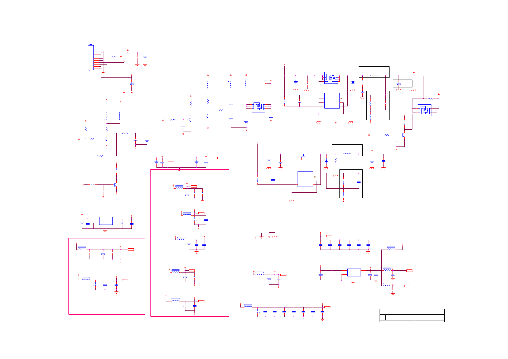
Power
2006/5/3
CN701
ON/OFF
1
2
BRIGHT
3
4
5
6
R721
7
8
9
10
11
12
CONN
+5V
L719
+5V
R707
10K 1/10W
ADJ_PWM5
ON_PBACK4
C770
22uF/16V
+3.3AVDD
+3.3AVDD
+5V_PANEL
L704
120 OHM
+
2006/5/3
L705
120 OHM
22uF/16V
4.7K 1/10W
0.1uF
2006/5/3
C724
120 OHM
R705
R713
NC
ON/OFF
R702
10K 1/10W
C706
0.1uF
GND
Vcc3.3 for
Digital
U702
3
VIN
VOUT
1
C717
ADJ
pin162,pin182
C767
+
C721
22uF/16V
0.1uF
pin66
+
C725
0.1uF
+3.3DV1=>LCD I/F Pad
+3.3DV2=>Host bus
2006/5/3
1K 1/10W
R703
1K 1/10W
Q704
PMBS3904
GND
22uF/16V
+3.3V_VDD
+5V_PANEL
GND
2
C718
+3.3DV1
C722
0.1uF
+3.3DV2
C726
PS_ON 4
+5V_PANEL
L720
NC
R704
1K 1/10W
R701
10K 1/10W
Q701
PMBS3904
+
C723
0.1uF
0.1uF
C701
NC
+12V
+3.3V_VDD
+3.3DV2
+18V
C702
NC
+
GND
C719
0.1uF
+3.3DV1 5
C704
+
C703
0.1uF
22uF/16V
+12V
L701
NC
+5V_PANEL
R706
ON_PANEL4
4.7K 1/10W
C709
+5V
C714
0.1uF
+3.3AVDD for
AVDD_DVI
+3.3AVDD for
AVDD_PLL
+3.3AVDD for
AVDDA
3.3V(6251) for
AVDD_PLL2
+3.3AVDD
+3.3V for
VDD_MPLL
+3.3AVDD
0.1uF
Vcc3.3 for
Analog
U701
3
VIN
1
ADJ
+3.3AVDD
22uF/16V
+3.3AVDD
L709 120 OHM
22uF/16V
L710
120 OHM
C737
22uF/16V
GND
VOUT
L706
120 OHM
C727
+3.3AVDD
L707 120 OHM
L708
120 OHM
C732
22uF/16V
AVDDPLL2
C735
2
C715
22uF/16V
AVDD_DVI
+
C730
22uF/16V
+
+
AVDD_PLL
+
PLL_GND
PLL_GND
BRIGHT
C707
+
C708
0.1uF
22uF/16V
+
C769
22uF/16V
5
R708
10K 1/10W
Q702
PMBS3904
+
pin4,pin10
AVDD_DVI 5
C728
0.1uF
+
PLL_GND
C733
0.1uF
pin109
AVDDPLL2 5
C736
0.1uF
VDD_MPLL
C738
0.1uF
+3.3AVDD
C729
0.1uF
AVDDA
Q705
PMBS3904
GND
C716
0.1uF
AVDD_PLL 5
pin12
C731
0.1uF
pin17,pin34
C734
0.1uF
pin204
VDD_MPLL 5
R714
100K 1/10W
AVDDA 5
R710
100K 1/10W
+3.3AVDD 4
+5V_PANEL
L702
120 OHM
C710
0.068uF
+1.8V_VDD
C711
NC
Audio PLL
1.8V
1.8V for
VDDC
+18V
L703
Panel_Power
5
NC
Q703
1
2
3
4
+
C712
22uF/16V
GND
+5V
PLL_GND
+1.8V_VDD
L711 120 OHM
pin49
pin63,pin79,pin131,
pin156,pin173,pin185,pin195
L712
120 OHM
+
C745
22uF/16V
R606
33K 1/16W
+12V
Q601
8
1
7
2
6
AGND
ISENSE
3
4
C617
0.1uF
3
4
FB
3
N.C
2
1
+2.5MVDD
+2.5MVDD
C754
0.1uF
+5V
C753
22uF/16V
VDDC
C751
0.1uF
5
U602
LM3485
VIN
PGATE
PWGND
ADJ
D602
SSM54
C755
0.1uF
VDDC 5
FB
N.C
AGND
ISENSE
GND
R605
22 1/16W
C614
0.001uF
+2.5MVDD 5
C763
0.1uF
layout together
C756
0.1uF
4
3
2
1
L602
22uH
R607
15K 1/16W
R608
31.6K 1/16W
GND
pin86, pin102,pin113
,pin125,pin139,pin154
U705
3
1
GM6605-2.5V
8
7
6
5
+
C752
0.1uF
+VLCD
8
7
6
5
C713
0.1uF
GND
+
C610
22uF/16V
C613
0.001uF
GND
+APLL
+
C743
22uF/16V
PLL_GND
C747
C746
0.1uF
0.1uF
+
C616
22uF/16V
R611
33K 1/16W
C615
0.001uF
Q602
AO3401L
2
+APLL 5
C748
0.1uF
1
U601
LM3485
8
VIN
7
PGATE
6
PWGND
5
ADJ
C750
C749
0.1uF
0.1uF
C601
0.1uF
C744
0.1uF
layout together
2/2
4.7K 1/10W
GND
+2.5MVDD
2.5V
FOR
DDR
C765
0.1uF
C766
0.1uF
+
+5V_PANEL
R716
2006/5/3
C620
100uF/25V
Q706
PMBS3904
+5V_PANEL
C621
0.001uF
2006/5/3
1
2
3
4
+2.5V_DMC 3
+2.5V_DMQ 3
Q708
2006/5/3
+5V
R724
NC
8
7
6
5
B
66Monday, June 19, 2006
of
L601
22uH
R612
22 1/16W
D601
SR54
C618
0.001uF
R613
30K 1/10W
C619
0.001uF
R614
10K 1/10W
CLOSE TO U602
GND
R715
ON_DDR
ON_DDR4
C611
0.001uF
C757
C758
0.1uF
0.1uF
2
VIN
VOUT
ADJ
C772
22uF/16V
4.7K 1/10W
C773
+1.8V_VDD
2/2
CLOSE TO U601
C759
0.1uF
+2.5VM
0.1uF
C612
+
C609
0.001uF
100uF/25V
L713
120 OHM
L714
+2.5V_DMC
120 OHM
+
C764
0.1uF
L715
+2.5V_DMQ
120 OHM
Title
MST9251A/HA
Size Document Number Rev
C
06.POWER
Date: Sheet
48
Page 49

Power board
49
Page 50
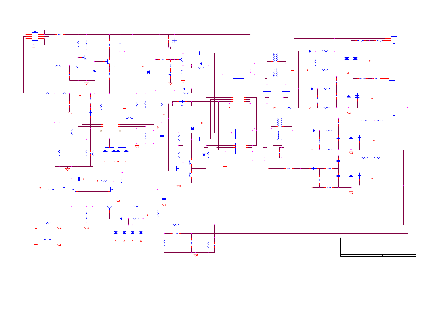
CN801
CONN
2
1
4
3
6
5
SST
R815
10KΩ 1/8W
JP801
0 1/10W
JP802
NC
R851
0 1/8W
10K 1/8W
NC
C821
F801
0 1/4W
R809
RK7002
Q812
R816
NC
R833270K 1/10W
300K 1/8W
C806
NC
C811
R828
C822
R801
OSP
1uF
10K 1/10W
2.2uF/16V
Q813
RK7002
C823 0.001uF
C827
560pF
Q804
PMBS3904
D809
LL4148
CT
R845 1M 1/8W
R802
10K 1/8W
Q801
PMBS3904
R818
R8341M 1/10W
200KΩ 1/4W
C824 0.01uF
+5V
R803
470 1/4W
ZD801
RLZ5.6B
R823
10 1/8W
IC801
1
DRV1
2
VDDA
3
TIMER
4
DIM
5
ISEN
6
VSEN
7
OVPT
8 9
NC1 NC2
OZ9938GN
BAV70PT
D813
R835
1
1M 1/10W
VS1
R852
300K 1/4W
Q818
RK7002
C828 0.1uF/25V
LL4148
C802
1000uF/16V
Q803
PMBS3904
+5V
R812
22 1/4W
PGND
DRV2
GNDA
SSTCMP
LCT
ENA
3
2
VS2
Q814
PMBS3904
D819
OP1
1uF/25V
1uF/25V
C833
+
16
15
14
13
CT
12
11
10
1
VS3
D818
LL4148
D820
LL4148
10 1/8W
3
2
VS4
Q817
PDTC144WK
LL4148
OP2
R826
D814
BAV70PT
R843
100K 1/10W
200K 1/10W
D821
OP3
D822
LL4148
R846
C836
OP4
R820
C815
+5V
100K 1/10W
0.01uF
D803
LL4148
+5V
R821
C816
1M5 1/4W
470KΩ 1/8W
C837
1uF/25V
4.7K 1/10W
R822
18K 1/10W
SST
C817
0.047uF
R850
R806
RK7002
D823
1KΩ 1/4W
13K 1/10W
C832
Q807
CT
330pF
1uF/25V
R808
0 1/10W
C818
RK7002
C835
NC
+
1000uF/16V
D805 LL4148
D808 LL4148
R824 39 1/10W
R836 0 1/10W
Q810
R844
5.6K 1/10W
R847
5.6K 1/10W
C803
Q802
PMBS3904
Q806
PMBS3906
R817 39 1/10W
D810
LL4148
R830
4.7KΩ 1/8W
R848
Q809
PMBS3904
Q811
PMBS3906
220 1/10W
C804
1uF
D804
LL4148
R810
39 1/8W
C819
1uF
D815
LL4148
0.1uF/25V
C801
R804 680 1/10W
1
<Title>
<Doc>
3
1
1
2
680 1/10W
3
2
3
3
D802
BAV99PT
R813
D807
BAV99PT
R827
680 1/8W
D812
BAV99PT
2
R838
680 1/8W
D817
BAV99PT
2
OP1
OP2
OP3
1KΩ 1/10W
OP4
5pF/3KV
D806
LL4148
LL4148
R807
D811
D816
3K 1/10W
R819
R805
100K 1/10W
R811 9.1K 1/10W
R814
100K 1/10W
3K 1/10W
R825 9.1K 1/10W
100K 1/10W
3K 1/10W
R831
R832 9.1K 1/10W
100K 1/10W
R840
3K 1/10W
R842 9.1K 1/10W
330pF
C805
1
C807
5pF/3KV
330pF
C810
C814
5pF/3KV
R829
330pF
C820
C825
5pF/3KV
R839
330pF
C826
Title
Size Document Number Rev
Custom
Date: Sheet
POWER X'FMR
PT801
4 6
C831
C808
4.7uF/16V
4.7uF/16V
OSP
2 1
2 1
4 6
POWER X'FMR
4.7uF/16V
C809
OSP
POWER X'FMR
4.7uF/16V
C834
PT802
C838
4.7uF/16V
PT803
4 6
2 1
2 1
4 6
PT804
POWER X'FMR
C840
4.7uF/16V
4.7uF/16V
R857
0 1/10W
4.7uF/16V
C841
R841
0 1/10W
Q805
AM4910N-T1-PF
4
5
G2
D2
3
6
S2
D2
2
7
G1
D1
1
8
S1
D1
Q808
AM4910N-T1-PF
4
5
D2
G2
3
6
S2
D2
2
7
G1
D1
1
8
D1
S1
+5V
R837
39 1/8W
C829
C830
R849
0.1uF/25V
220 1/8W
Q816
AM4910N-T1-PF
4
G2
3
S2
2
G1
1
S1
4
G2
3
S2
2
G1
1
S1
Q815
AM4910N-T1-PF
5
D2
6
D2
7
D1
8
D1
5
D2
6
D2
7
D1
8
D1
D801
LL4148
VS1
LL4148
C839
VS2
VS3
VS4
1
2
R855
1KΩ 1/10W
CN802
CONN
1
2
R853
1KΩ 1/10W
CN803
CONN
1
2
R854
1KΩ 1/10W
R856
CN804
CONN
1
2
CN805
CONN
ACER 22
INPCC42MA1P
11Saturday, July 29, 2006
B
of
50
 Loading...