

Page 1

AL702
Service G uid ervice
17-inch LCD Monitor
Page 2

AL502
1. Audio circuit (Circuit diagrams Main PWB)
1.1 Au dio input
Th e audio signal input recei v ed from the audio input terminal (JK011) is appl ied to the amplifi er I001 of 4 (LCH) an d 9 (R-CH) through the low-pass filt er consis tin g of R040, R041, R042, R043, C040 an d C041.
In this amplifier, controls of Volume and mute are conducted. The audio signal controlled at the pin 6 determines
th e attenuat ion of output of the amp lifiers. Since then, th e signal is output to th e jack P003.
1.2 Au dio output
Th e audio s ignal is output from P002 output terminal of the Audio block to the internal speaker system.
2. Power supply (Circuit daigrams MAIN PWB)
2.1 Line fil ter c onsist s of C801, T801, C802, C803, C804. It eli min at es hig h frequen cy interference to meet EM I’s
req uirement.
2.2 Rec & Filter :
Bridg e diode D801 converts AC source into pu lsed DC. This pulsed DC is smoothed an d filtered by C805.
R802 is an NTC ( negative thermal coefficient ) resistor, used to reduce inru sh current to be within safe range.
2.3 Powe r tran sformer :
T802 c onverts energy for square wave from power source C805 to secondary s ide to generate +12V and +5V.
2.4 Ou tput :
Th e square wave from T802 is rectified by D809, D810, then filtered by C817, C822 to generate +12V and
+5V res pectively.
2.4.1 A 5V power supply f or LCD modu le, CPU and logic i s g enerated from the power sou rce.
2.4.2 I308 : 3-terminal reg u lat or
A 3.3V power supply f or I306 an alog is generated from t h e 5V source.
2.4.3 I308 : 3-terminal reg u lat or
A 3.3V power s upply for I306 digital is generated from th e 5V source.
Q302, Q303 ON/OFF cont rol for LCD Modu le
ON/OFF con trol is performed for power ON/OFF and also for the power saving sequence.
2.5 Driv er :
Q803 drive T802 from PWM control of I801 for power convert ed.
2.6 FB :
Neg ative feedback CKT consi sts of photo coup ler I802 and adjus table regulator I803. It can maintain output
v olt ages +5V and +12V at a stable level.
2.7 PWM :
2.7.1 Start : When power is t u rned on, Q801 conducts due to bias from C805 and R805,R803. C807 is charged a 16
v olt and a starting current abou t 0.3mA to pin 7 of I801. I801 starts to oscillate and outputs a pulse train
th rou gh pin 6 to drive Q803.
2.7.2 OPP : Wh en Q803 turn s on, C805 supplies a linearly increasing tri angle current through th e primary induc
tan ce of T802 to the driver Q803, once th e peak value of this curren t multipl ied by R811 exceeds1 volt, pulse
tra in will be shut down i mmediat ely to protect Q803, T802 from being burned out.
2.7.3 Regulation : If ou tput voltage +5V goes up, the R terminal of I803 gets more bias, accordingly photo transis
tor an d photo diode flows more cu rrent. The voltage of pin 2 goes up too, making the pulse width of pin 6 to
become n arrower. So t he output voltage +5V will be pulled down to a stable value.
Page 1Circuit D escrip tion
Page 3

AL502
2.7.4 OVP : If +5V g oes up too much, the induced voltage on pin 4 of T802 becomes large al so. Suppose that it is
ov er 18 volts, ZD801 conducts, pin 3 of I801 is pulled up over 1 volt. The pulse train at pin 6 goes down to
zero, s h uttin g Q803 off immediately.
2.7.5 SCP : If ou tput terminal is short to ground, photo transistor does not conduct, hence Q806 does not conduct
either. Then oscilla tion of I801 is stop, sh utting Q803 off immediat ely .
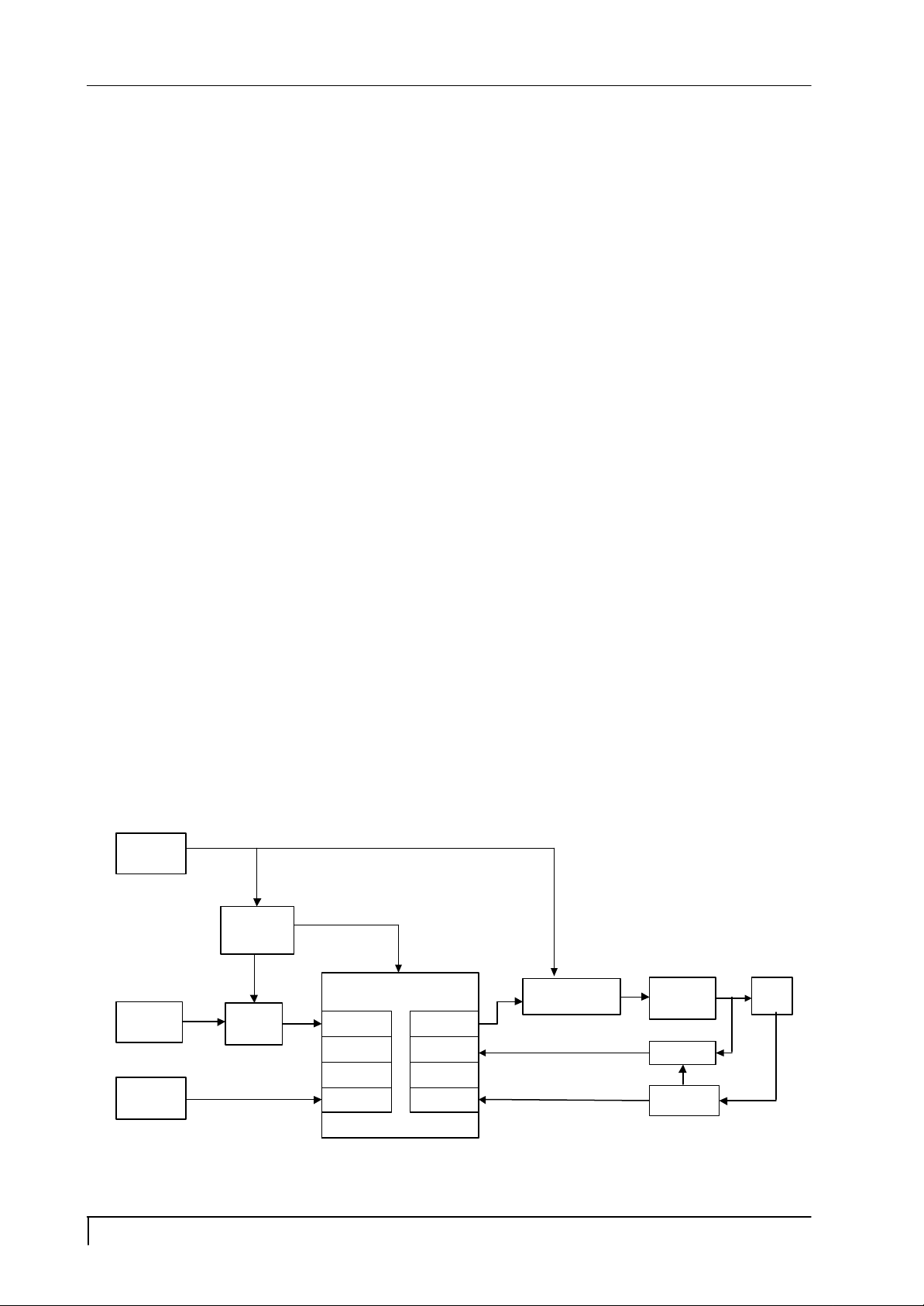
H15AAU / H15AAR Power Board Block Diagram
Line Filter
Rec.
&
Filter
PWM Driver
Power
Transformer
FB
Output Rec. & Filter
3. On-screen circuit (Circuit diagrams Main PWB)
I300 Emb eded f u ncti on.
On -screen menu screen is established and the resultant data are output from I300 (Circuit diagram MAIN PWB).
4. Video input circuit (Circuit diagram MAIN PWB)
Th e AC-coupled video signal is used to clamp th e black level at 0V).
5. Definition converter LSI peripheral circuit (Circuit diagram MAIN PWB)
I301 MRT V2 gmZAN1 is the defi n ition A/D con verter LSI.
Th e analog R, G, B signal input entered from the video input circuit i s convert ed in to t he digital data of v ideo
s ign al throu g h the incorporated A/D converter. Based on t his conversion, this device performs i nterpolation
du ring pixel extension. The source voltage for this device is 3.3V and the sy stem clock f requ ency is 12MHz.
Th e with stand voltage level for the input signal voltage is 3.3V and 5V.
6. System reset, LED control circuit (Circuit diagram MAIN PWB)
6.1 Sy stem reset
Sy stem reset is performed by detecting the risin g and falling of the 5V source voltage at I302.
6.2 LED control circ uit
Gre en / amb er i s li t with t h e control s ignal of th e LED GREEN and LED A M BER sig n al p in 43, 42 from I303
(Circui t diagram MAIN PWB).
7. E2PROM for PnP (Circuit diagram MAIN PWB)
Page 2 Circuit D escrip tion
Page 4

8. E2PROM (Circuit diagram MAIN PWB)
Data trans fer between I304 and CPU (Circui t diagram MAIN PWB page 4/7 (I303) is effected throu g h the IIC
bu s SCL (pin 9) and SDA (pin 8) of I300 or SCL (pin 42) and SDA pin 39 of I301. The data to be transferred to
each device are stored in I304.
n I300 control data.
n OSD related s etting data.
n Other con trol data for serv ice menu.
9. CPU circuit (Circuit diagram MAIN PWB)
I303 (MTV312M64) (SM89516C25) or (W78E62BP-40) fun ctions as the CPU.
Th e source voltage for th e device is 5.0V and the system clock frequ ency is 12MHz.
9.1 Detection of POWER switch status
Th e CPU identifies the ON status of the two power supp lies. The identification is made when the power supply
is turned off. For example, if the power supply is turned off with the POWER switch, the POWER switch must be
tu rned on when activating t he power supply again. If the power supply is turned off by pull in g out the power
cord , then th is power s upply can be turned on by con necting the power cord, wit hout pressing the POWER
s witch.
9.2 Dis pl ay mode i den tification
9.2.1 Functions
(1) Dis play mode identification
n The display mode of input signal is identified based on Table 1, and according to the frequency and polarity
(HPOL, VPOL) of h orizontal or vertical sync signal, presence of the horizontal or vertical sync signal, and the
discriminati on sig n al (HSYNC_DETECT, VSYNC_DETECT).
n When the mode has been identified through the measurement of horizontal and vertical frequencies, the total
n umber of lines is determined with a formula of “ Horizont al frequ ency / Vertical frequency = Total number
of lin es. “Fin al i den t ificatio n can be made by examini n g t he coincidence of th e obtain ed figure wi th the
n umber of lines for the mode identified fro m the frequ en cy.
n When the detected frequency if the sync signal has changed, the total number of lines should be counted even
th rough it is rge ident ified frequency in the same mod e. Then, it is necessary to examine whether th e preset
v alue for the vertical dis play positi on o f It em 4-3 has exceeded th e tot al number of lin es. If e xceeded, a
maximu m value shoul d be set up, which does n ot exceed the vertical display pos ition of Item 4-3.
(2) Ou t-of -range
Th is out-of-range mode is assumed when the frequency of the horizontal / vertical signal is as specified below.
n Vertical frequ ency : Below 50Hz or above 85Hz
n Horizontal frequency : Bel ow 24 KHz or above 75 KHz
AL502
(3) Power s ave mode
Th e power save mode is assumed when the horizontal / verti cal signals are as specified below.
n If there is no horizon tal sync signal input.
n If there is no vertical sync signal input.
n If the horizontal sync sig nal is outside th e measuring range of I300.
n If the vertical sync sign al is outside the measuring range of I300.
Page 3Circuit D escrip tion
Page 5

Table 1
Pin No.
Signal name
Mode
H-
freq
(
KHz)
Band Width
31.47
31.47
31.47
37.86
35.16
37.88
46.88
48.08
49.72
48.36
52.45
56.48
60.02
AL502
No Resolution
(MHz)
1. 247 VGA 720 x 350 70Hz
2. 102 VGA 720 x 400 70Hz
3. 103 VGA 640 x 480 60Hz
4. 182 MAC 640 x 480 66Hz 35 32.24 - -
5. 173 VESA 640 X 480 72Hz
6. 109 VESA 640 X 480 75Hz 37.5 31.5 - -
7. 104 VESA 800 x 600 56Hz
8. 116 VESA 800 x 600 60Hz
9. 110 VESA 800 x 600 75Hz
10. 117 VESA 800 x 600 72Hz
11. 108 MAC 832 x 624 75Hz
12. 118 VESA 1024 x 768 60Hz
13. 217 SUN 1024 x 768 65Hz
28.322 + -
28.322 - +
25.175 - -
31.5 - -
36 + +
40 + +
49.5 + +
50 + +
57.283 - 65 - -
70.49 - -
Polarity
H V
14. 157 VESA 1024 x 768 70Hz
15. 141 VESA 1024 x 768 75Hz
Atten tion :
1. Wh en resolution beyond 1024 x 768 is inpu tted, resolution is lowered with Down scaling to 1024 x 768, and
in dicat ed, and OSD should indicate OUT of Range.
9.3 Us er Control
9.3.1Related ports of I303
Port
P1.5 7 I POWER Power switch input Power ON , OFF
P1.1 3 I DOWN switch input ( ) key
P1.0 2 I UP switch input ( ) key
P1.3 5 I - - switch input ( - ) key
P1.2 4 I + + switch input ( + ) key
I/O
Function Remarks
75 - -
78.75 + +
control
Page 4 Circuit D escrip tion
Page 6

9.3.2 Functions
Pin No.
Signal name
Pin No.
Signal name
Con trol is effected for the push-switches to be used when the user changes the parameters, in order to modify the
res pecti ve setting values. Whether the s witch has been pressed is identi fied with the switch input level th at is
tu rned “L”.
Each switch in put port is pulled up at outside of ASIC.
Each parameter is stored i n the EEPROM, the contents of which are updated as required.
9.4 Con t rol of defini tion converter LSI I300.
9.4.1 Ports related to control
AL502
I/O
159 I IRQ interrupt signal
5 I/O SCL serial clock
6 I/O SDA serial data
9.4.2 Functions
Majo r functi on of I300 are as foll ows:
(1) Expansion of the display screen.
(2) Timing control for various signal types.
(3) Power-s upply sequence (LCD panel).
9.5 I2C bu s control
9.5.1 Re lated ports of I303
Port
P1.7 14 O SCL IIC bus clock
P1.6 13 I/O SDA IIC bus data
9.5.2 I2C-con trolled functions
Th e following functional controls are effected by I2C.
(1) Con t rol o f EEPROM I304 for p arameter setti ng.
I/O
Function
Function
Page 5Circuit D escrip tion
Page 7

9.6 Power ON s equence
POWER
D-SHCLK
DATA
Wh en the POWER switch is pressed, the POWER OFF signal is turned “H”. When this “H” potential is detected,
th e CPU begins to establish the respective power supplies according to the sequence shown below.
PPWR
INV_EN
LED
AL502
Page 6 Circuit D escrip tion
Page 8

9.7 Power OFF s equence
POWER
D-SHCLK
DATA
Wh en the POWER switch is pressed while the power su pply is ON, the POWER ON signal is turned “H”. When
ts hown below.his “H” potential is detected, the CPU begins to turn off the respective power supplies according
to the sequence
PPWR
INV_EN
AL502
LED
Page 7Circuit D escrip tion
Page 9
AL502
10. Inverter
Th is unit operates on an output v oltage of 15V from po wer source.
10.1 Regulator: Q101 get a +5VDC for I102 power supply.
10.2 UVP: Q106 tu rns off when the Vin is under 14V. Then pin 3 of I102 is pulled low and inverter off immedi ately.
Th at is the under voltage protection.
10.3 Co ntrol IC: I102 (OZ960S)
10.3.1 Enable : Wh en pin 3 of I102 is ov er 1.5V, I102 works. If it is under 1.5V, I102 tu rns off.
10.3.2 OSC: When I102 enabled, R108/C115 (pin 17/pin18 of I102) dete rmine the operat ing frequen cy .
10.3.3 SST: C104 (pin 4 of I102) provides soft start funct ion .
10.3.4 Ignit ion : R109 (pin 8 of I102) provides higher operatin g frequency for more striking vol tag e unt il regulation
of f eedbac k of l amp cu rren t. C103 (pin 1 of I102) determi ne the striking time.
10.3.5 Dimming control: The di v ided voltage of R106/R105/R104 control the duty pulse of burst-mode to drive Q105
and perform a wide di mmin g control for the CCFL. T he burs t-mode frequ en cy is d etermin ed by C116.
10.3.6 Regu lation : Pin 9/pin 10 of I102 provide regulat ion of t h e CCFL curren t from feedback. Th e n on-inverting
reference (pin 10 of I102) is at 1.25V nomin al.
10.3.7 Protecti on : Open-lamp protection in t he ignition period is provided through both pin1 and pin 2 of I102.
Remov al of th e CCFL during normal operatio n will tri gger Q104 to turns on and shu ts off the inverter. This
is latch f unction.
10.3.8 Output drivers: The configuration prevents any shoot-through issue associated with bridge-type power
con version applications. Adjusting the overlap conduction between I101 P-MOSFET and I103 N-MOSFET,
I101 N-MOSFET an d I103 P-MOSFET, the CCFL curren t reg u lation is achiev ed.
10.4 Fu ll-bridge swit ching /Transformer: I101/I103 /C123/C125/T101/T102 compose f ull-bridge swit ch ing to
con vert DC into AC for driver the CCFL.
10.5 Detection : C124/C119/CR102 detect the output voltage and ensure a rated voltage by pin2 of I102. Q102/Q103
en sure not a open -lamp.
10.6 Feedb ack: CR101/R120/R121/D108 sense the l amp cu rren t for neg ativ e feedback and regulation. The di vided
voltag e on R121 will be at 1.25V.
Inverter Board Block Diagram
VCC
Regulator
VDD
ON / OFF
Brightness
control
Control IC : OZ960
U.V.P. Enable
OSC
SST
Dimming
control
Output driver
Protection
Ignition
Regulation
Full-bridge switching
Transformer
Detection
Feed back
Lamp
Page 8 Circuit D escrip tion
Page 10
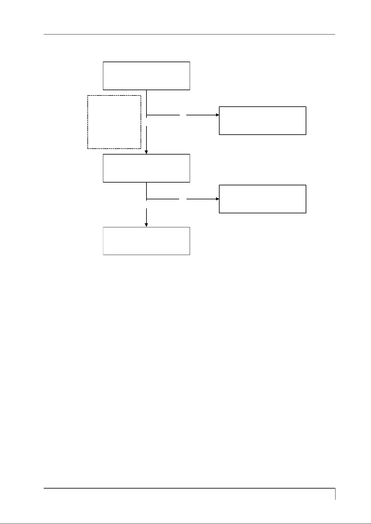
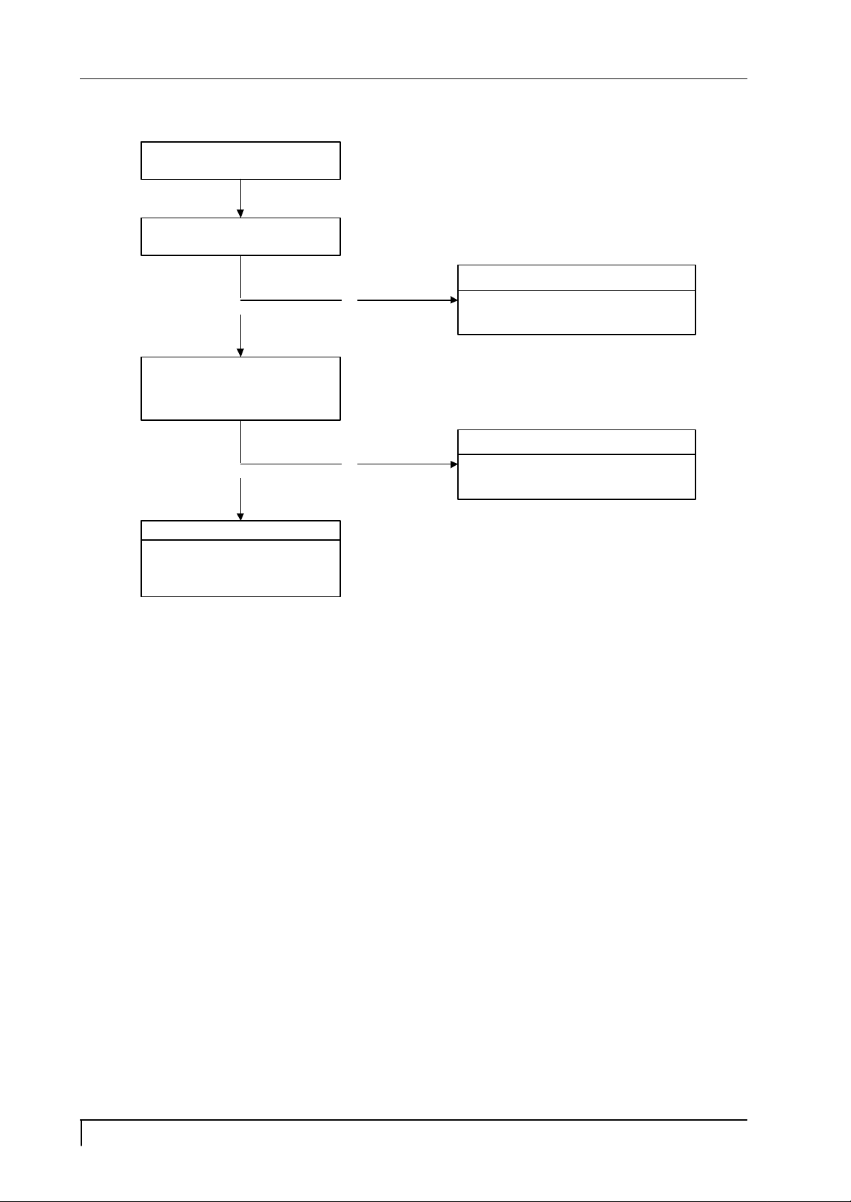
1. No display of screen (Screen is black, color of LED is amber)
Does OSD display when
you push key button.
When a signal isn't
being inputted, it is
indicated with "VIDEO
INPUT". It is indicated
with "OUT OF RANGE"
at the time of the
frequency that it can't be
distinguished.
Check if the sync signal from Computer
is output and if the video cable is
Yes
connected normally.
No
Proceed "No OSD display"section.
ALC502
OK
NG
Proceed "Checking the resolution change
IC movement" section.
Input the sync signal of computer, or
change the cable.
Trouble Sh ooting Page 1
Page 11
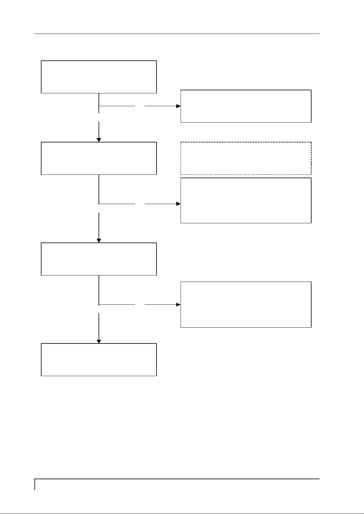
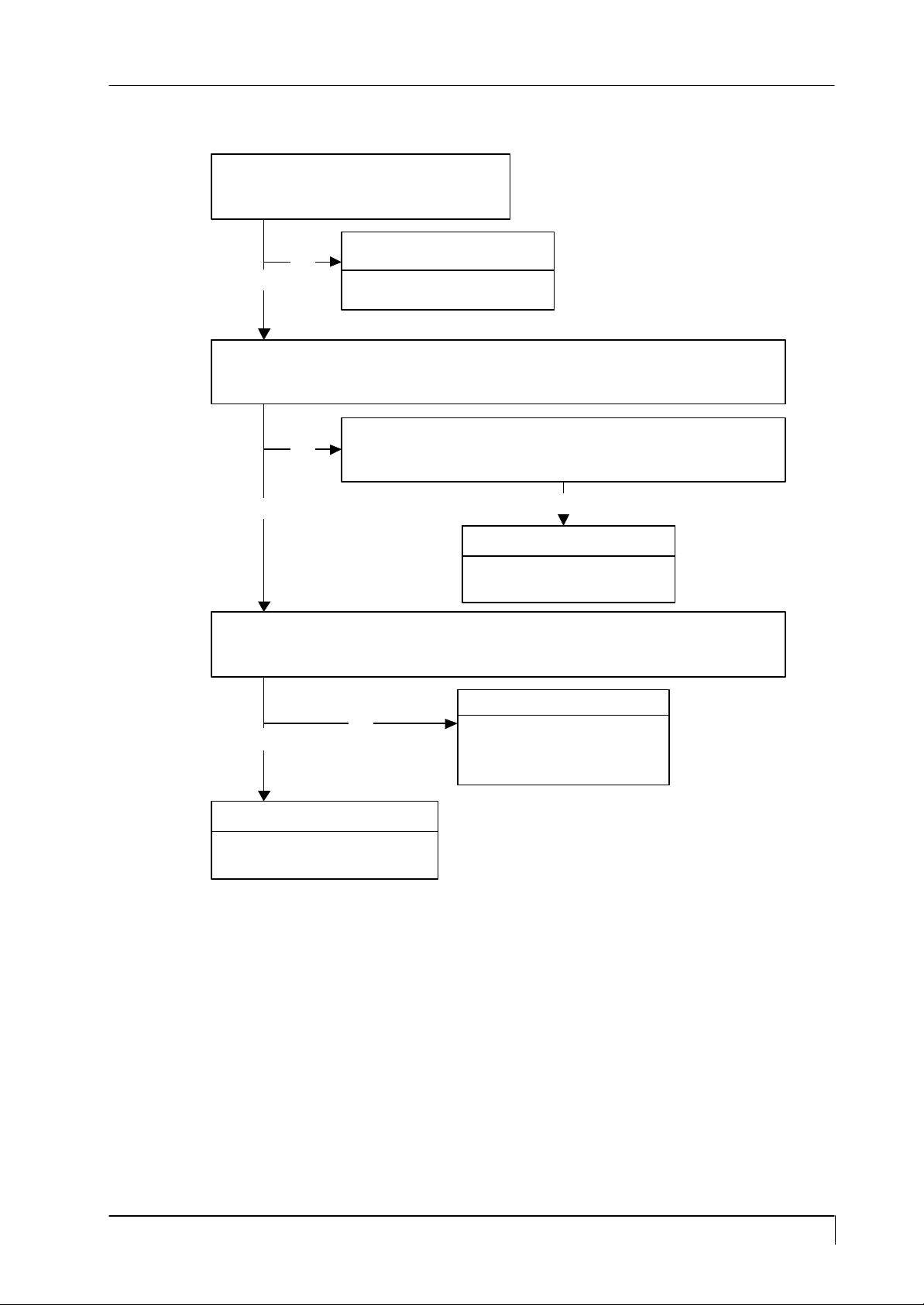
2. Nothing displays on screen (Screen is black, color of LED is green)
Is backlight lit?
NG Refer "Checking the backlight unit" section
OK
ALC502
Does computer output RGB video signals?
OK
Check OSD menu is displayed on screen
when you push the "PROCEED" key.
OK
NG
NG
Check the video cable for failure. Check the host for
output signal with all black only.
1) Change pattern of video signal output on the
host.
2) Reconnect the video cable.
3) Change the video cable.
Next Page
Proceed "Abnormal screen" section.
Page 2 Trouble Sh ooting
Page 12
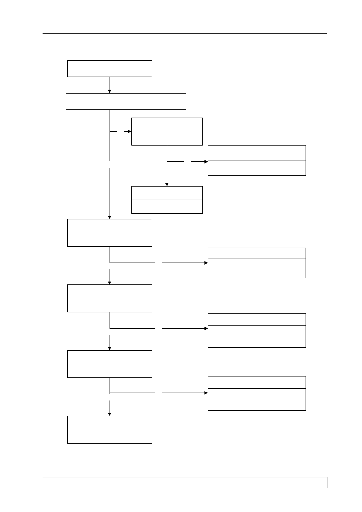
Continue
2) Printed wire broke between I302 and P303 pin 44.
2) Printed wire broke between I300 and P303 pin 38.
2) Printed wire broke between I300 and P303 pin 40.
Check the 3.3 V power are supplied on I308 pin 2.
Check if the voltage on I308 pin3 that
NG
OK
is high level DC at 5V.
OK
Failure point
NG
ALC502
Failure point
1) Printed wire broke between P301 and I308
I308 Failure
Is a dot clock being outputted under the
condition that a LCD module is connected to
Check the H-sync pulse of negative polarity is
output on P303 pin 38 at TTL level.
Check the V-sync of negative polarity are
P303 pin 44?
OK
OK
output on P303 pin 40.
NG
NG
Failure point
1) I300 failure
Failure point
1) I300 failure
Next Page
Trouble Sh ooting Page 3
OK
NG
Failure point
1) I300 failure
Page 13
Continue
Check the data enable of positive polarity
are output on P303 pin 42.
OK
Check the data signal output on P306 and
P303 R, G, B data pin.
NG
ALC502
Failure point
1) I300 failure.
2) Printed wire broke between I300 and P303 pin 42.
Failure point
OK
Failure point
1) The cable broke between P303 , P304
and LCD module.
2) LCD module failure.
NG
1) I306 failure.
2) Printed wire broke between I300 and P303 , P304
data line
Page 4 Trouble Sh ooting
Page 14
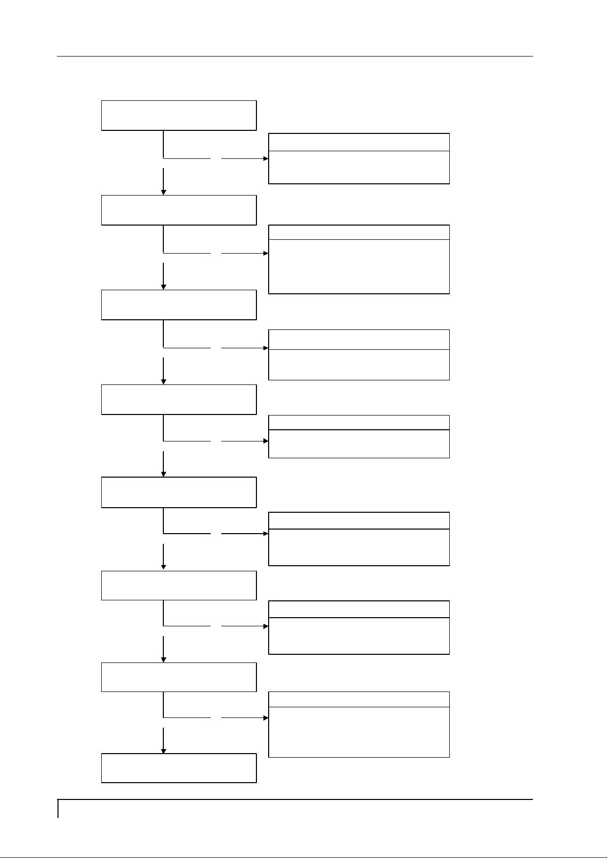
3. Checking the back light unit
Is +15V supplied to P803
pin 3, 4 to inverter PWB?
ALC502
NG
OK
Check the INV_EN signal of the rectangle input I307 pin 5 at TTL high level
NG
OK
Check the PWM signal of the input from I303 pin 7 is a BRI signal
Inverter cable disconnection.
Failure point
Is a "H" level being output in the TTL level from I300 pin 143
Or, is INV_EN signal of the rectangle being output?
NG
Failure point
Printed wire broke between
I300 pin 143 and I307 pin 5
OK
NG
Failure point
1) Inverter cable disconnection.
2) Inverter of LCD module failure.
Failure point
1) Printed wire broke between
I303 pin 17 and I307 pin 3
2) I307 failure.
Trouble Sh ooting Page 5
Page 15
4. Abnormal screen
ALC502
Check the R, G, B video signal from computer input on
Check the R, G, B input signals on I301 pin 12, 20, 28,
Is the pulse of the TTL level being output to P303, P304
Check the negative horizontal sync pulse output to P304
D-Sub R, G, B connector.
OK
respectively that their level is 0.7Vp-p maximum.
OK
from the data line of I300?
OK
pin 38 from I300 pin 80 at TTL level.
NG
NG
NG
Failure point
1) No R, G and B video signal output from host computer. Check
computer
2) Video signal cable disconnection.
Failure point
In case of the Red signal. (A Green and Blue signal is the same
path, too.)
1) Printed wire broke between D-Sub(R) and I301 pin 12.
2) R341 short.
3) C321 open.
4) R362 open.
Failure point
1) Printed wire broke between I300 data line and P303, P304
2) I317 failure.
OK
Check the negative vertical sync pulse output to P304 pin
40 from I300 pin 75 at TTL level.
OK
Check the positive DE pulse output to P304 pin 42 from
I300 pin 74 at TTL level.
OK
Check the SHFCLK OUTPUT to P304 pin 44 from I300
pin 44 at TTL level.
OK
Process "Checking the resolution change IC movement"
section.
NG
NG
NG
NG
Failure point
1) Printed wire broke between I300 pin 80 and P304 pin 38.
2) R351 open
Failure point
1) Printed wire broke between I300 pin 75 and P304 pin 40.
2) R352 open
3) C416 short
Failure point
1) Printed wire broke between I300 pin 74 and P304 pin 42.
2) R355 open
3) C382 short
Failure point
1) Printed wire broke between I306 pin 44 and P307 pin 44.
2) FB314 open
3) FB315 open
4) C380 short
5) C381 short
Page 6 Trouble Sh ooting
Page 16
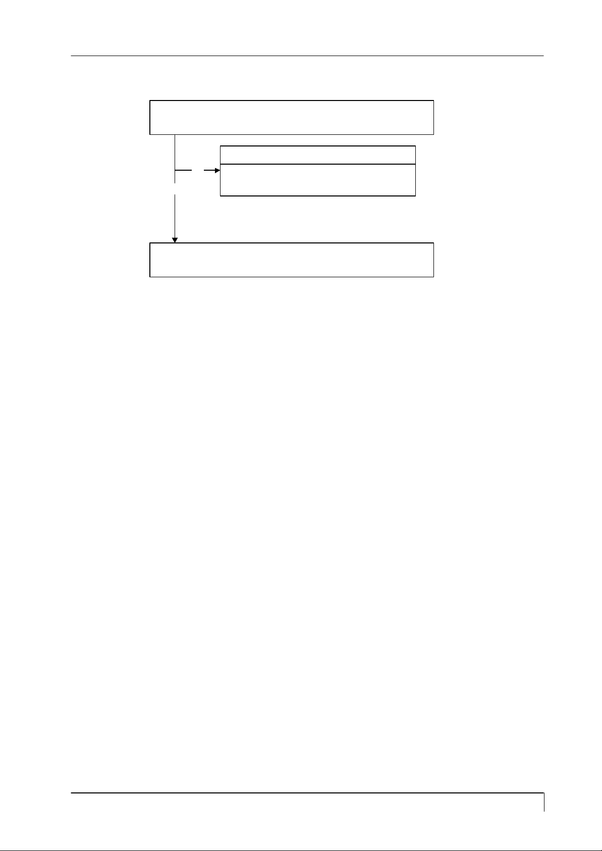
5. NO OSD display
Check the input of pulse from I300 pin 5, 6.
Failure point
NG
1) Printed wire broke between I306 pin 5 and I303 pin 9.
OK
2) Printed wire broke between I306 pin 6 and I303 pin 8.
Proceed "Checking the resolution change IC movement" section.
ALC502
Trouble Sh ooting Page 7
Page 17
6. Abnormal plug and play operation
6.1 Abnormal DDC2
Confirm the input of serial data on I305 pin 6 synchronize SCLK at TTL level.
ALC502
NG
OK
Failure point
1) The host machine isn't communicating in DDC2 mode.
2) The video cable may have failed or may not to have connections for DDC.
3) Between I305 pin 6 and P302 pin 15 may have failed.
4) R337 open.
5) Cable failure.
Failure point
I305 failure.
Page 8 Trouble Sh ooting
Page 18
7. Checking the interface circuit of sync signal
7.1 Checking the control circuit of horizontal sync pulse
ALC502
Check the horizontal sync signal on I301
Process "Checking the resolution change IC
pin 94 TTL level.
NG
OK
movement" section.
1) Video cable may have failed.
2) Printed wire broke between P302 pin 13
and I301 pin 94
3) R346, R348 open
4) C372, C373 short
7.2 Checking the control circuit of vertical sync pulse
Failure point
Check the vertical sync signal on I300 pin
Process "Checking the resolution change IC
44 TTL level.
NG
OK
movement" section.
Failure point
1) Video cable may have failed.
2) Printed wire broke between P302 pin 7 and I300 pin 44
3) FB308, R343 open
4) C369 short
Trouble Sh ooting Page 9
Page 19
8. Checking the resolution change IC movement
Is there +3.3V supply on I300 pin 17, 21, 57, 77, 79, 97, 102, 117, 137, 154, 156, 157 and 65.
ALC502
NG
OK
Is 12MHz clock input to I300 pin 3 at
NG
OK
Is +5.0V supplied to I300 pin 2 at
NG
OK
Failure point
I300 failure
Proceed "Checking the DC/DC converter circuit" section.
TTL level?
Is 12MHz clock output from X300
OK NG
Print wire broke between X301 and
High level?
Check the output of 5.0V "H" pulse
from I302 pin 6.
NG Is 5.0V supplied to I302 pin 7?
OK
at TTL level?
Failure point
I300 pin 3.
OK
Failure point
X300 failure
NG
Failure point
1) FB319 open
2) Power source
Failure point
Print wire broke between I302 pin 6
and I300 pin 2.
Failure point
I302 failure
Page 10 Trouble Sh ooting
Page 20
9. No power on
9.1 No power on (I)
Check output voltage +5V,
+15V is right or not.
ALC502
NG
Check power switch is turn on
OK
Check power cord ( P801), Signal cable
(P302),P802, P803, CN102, CN103
is connected right or not.
OK
Check C805 is about DC
OK
OK
OK
or not.
NG
NG
140V-330V or not.
NG
Check C807 is over
10V or not.
NG
It is not power board
problem.
Turn switch on.
Connect it right.
Check F801, D801, P801
and repair them.
Check R805, R803, I801
and repair them.
Check pin 6 of I801 have
same pulse or not.
OK
Check pin 1 of T802 have
same pulse or not.
OK
Check peak voltage of R811 triangle
pulse is up to 1 volt or not.
OK
Check D809, D810, C816, C821, T802
have same short circuit, or the output
+5V, +15V is over load.
NG
Check feedback circuit around I802,
I803 and the other components
and repair them.
NG
NG
NG
OK
Check peripheral components
of I801 and repair them.
Check Q803, R813, R814, D806
, R812 and repair them.
Check D804, R807 and
repair them.
Repair them.
Trouble Sh ooting Page 11
Page 21
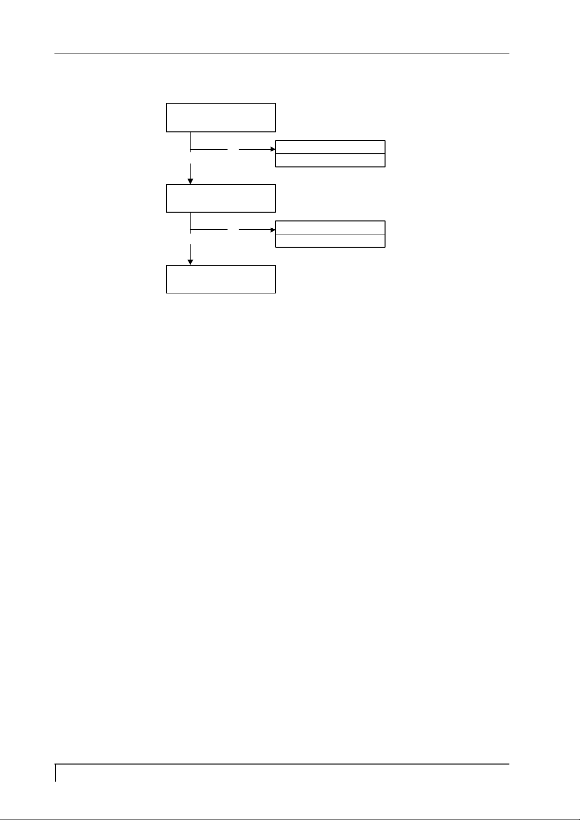
9.2 No power on (II)
ALC502
Check the + 5V power is supplied
from power source.
OK
NG
Is LED turned on in amber
momentarily when a power button is
pushed?
NG
OK
Proceed "Checking the operation of
CPU".
Failure point
Power source failure.
Failure point
Power source failure.
Page 12 Trouble Sh ooting
Page 22
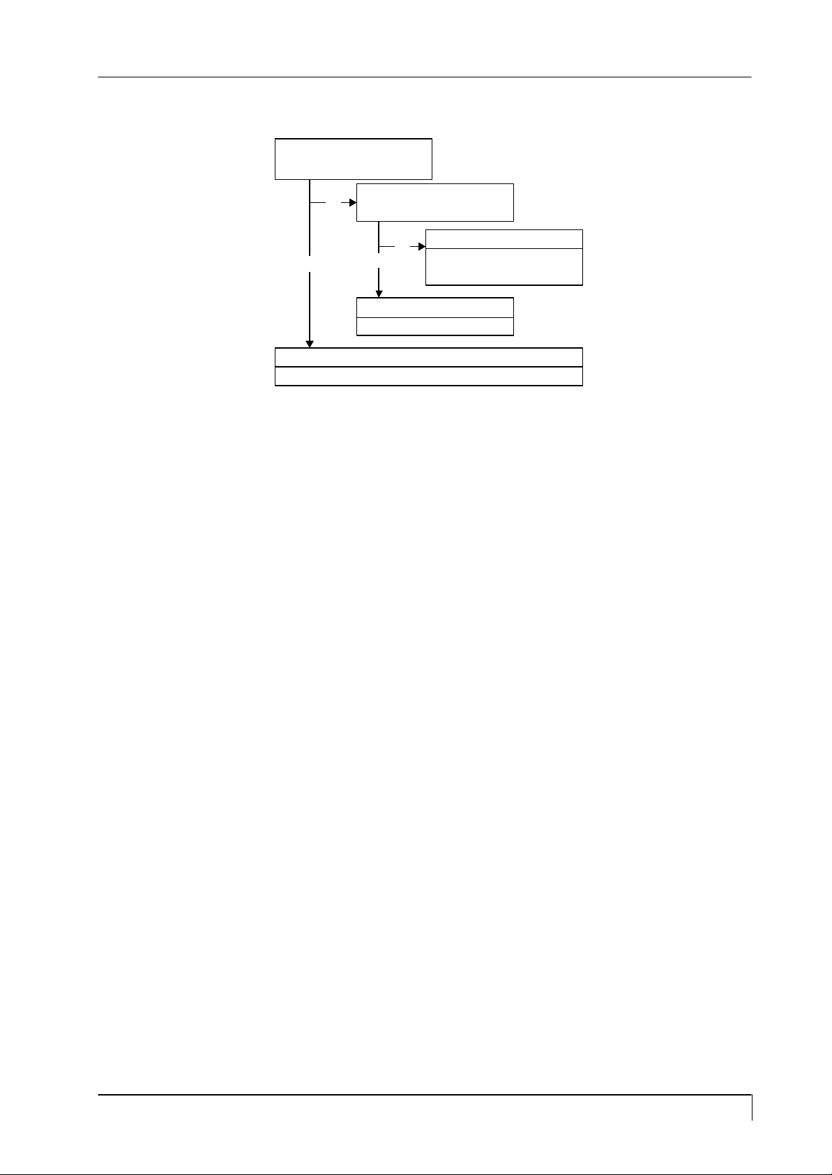
10. Checking the DC/DC converter circuit
ALC502
Check the output of 3.3V line voltage
from I308 pin 2.
Is the output FB321 being inputted
NG
OK
Printed wire broke between I308 pin 2 and I300 power supply pin.
OK
to I308 pin 3?
NG
Failure point
I308 failure
Failure point
Failure point
Printed wire broke between I308
pin 3 and output of FB322.
Trouble Sh ooting Page 13
Page 23
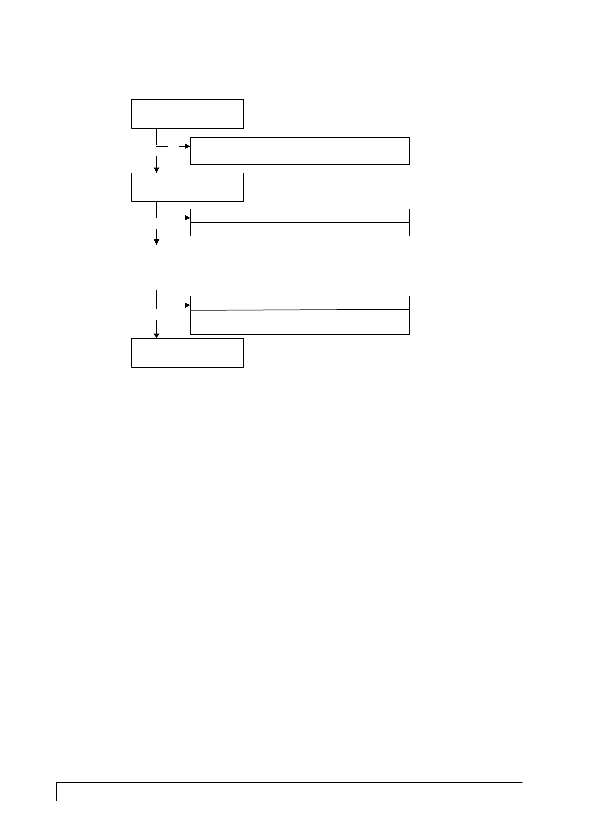
11. Checking the operation of CPU
Printed wire broke between output of FB320 and I300 power supply pin.
Is there +5.0V supply on I303 pin 44
ALC502
NG
OK
Is 12MHz clock input to I303 pin 21
and 20 at TTL level?
NG
OK
Check the input of 5V "H" pulse from
I310 pin 4 are same as I303 pin 10.
(14 msec Typ)
NG
OK
I303 failure.
1) Printed wire broke between I310 pin 4 and I303 pin 10.
Failure point
Failure point
X301 failure.
Failure point
Page 14 Trouble Sh ooting
Page 24
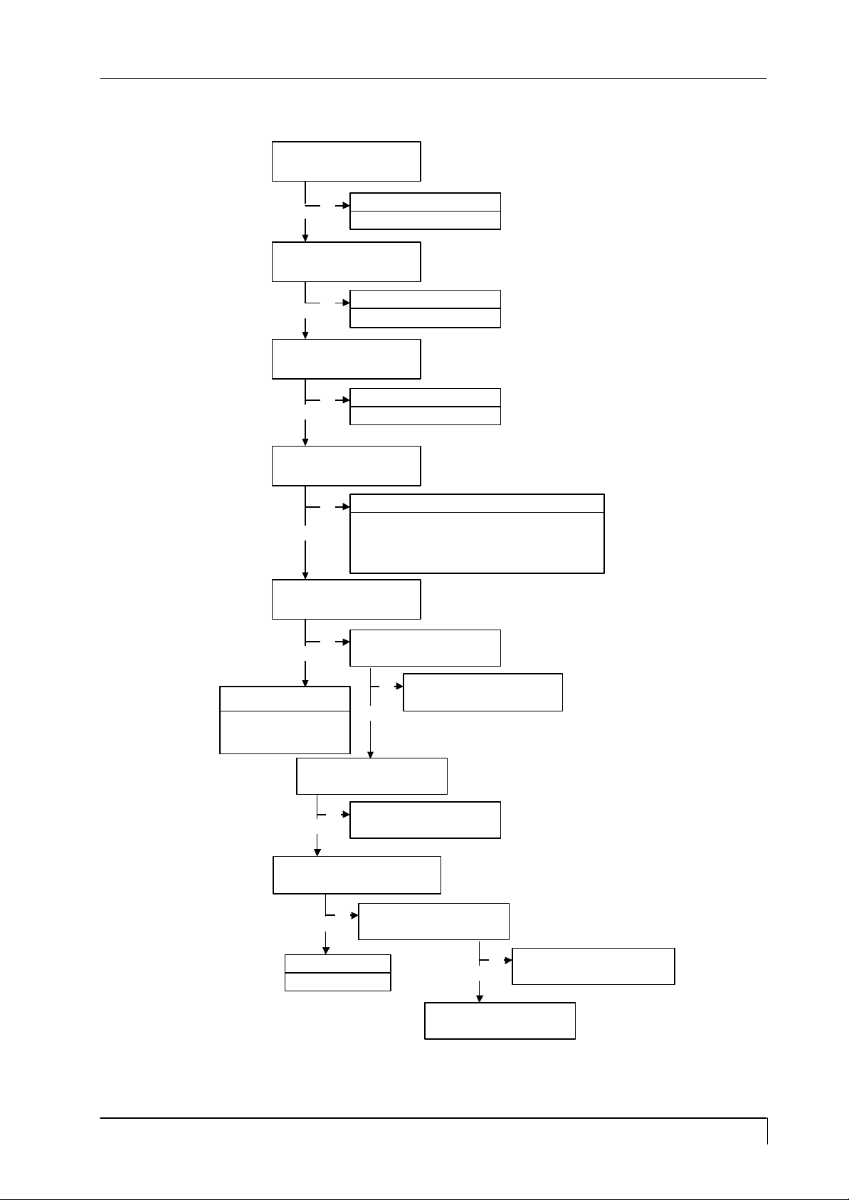
12. Checking the audio circuit
Is a cable with the
host PC connected?
ALC502
NG
OK
Aren't the setups of the
host PC a minimum and off?
NG
OK
Is correct output waveform
being inputted from JK011
pin 2, 3 of the host PC?
OK
Is the waveform which is the
same as JK011 being
inputted to I001 pin 4, 9?
OK
Is output wavefrom being
outputted in I001 pin 14, 17?
The setup of the host PC is changed.
NG
NG
1) Printed wire broke between JK011 pin 2, 3 and I001 pin 4, 9.
2) R040, R041 open.
3) R042, R043 short.
4) C040, C041 open.
Failure point
Audio cable disconntction.
Failure point
Failure point
Audio cable disconntction.
Failure point
NG
OK
Failure point
1) Speaker cable disconnection
2) Speaker failure
Is mute/STD-BY low level at pin 11,
OK
Is Variable DC volume
Failure point
Is 15V supplied to I001 pin 15, 16?
pin 12.
NG
control at pin 6.
NG
OK
I001 failure.
NG
Proceed section 9.1 "No power on".
OK
Proceed section 11 "Checking
the operation of CPU".
Check I002 pin 8 is 5V DC.
OK
Proceed section 11 "Checking
the operation of CPU".
NG
Proceed section 9.1 "No power on".
Trouble Sh ooting Page 15
Page 25
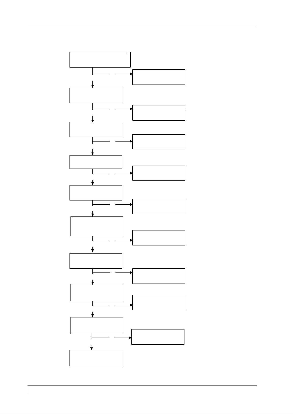
13. Checking inverter board circuit
Check Vin pin is around 15.5V.
Check Q101, D101, D104 and repair
Check Q106, D110 and repair them.
Check C115, R108, I102 and repair
Check Q102, Q103, CR101, CR103
On/off pin is over 2V.
Brightness pin is between 0V and 3.7V.
ALC502
OK
Check pin 5 of I102 is 5V.
OK
Check CN102, CN103 is connected
right.
OK
Check pin 3 of I102 is over 2V.
OK
Check pin 18 of I102 is triangle
pulse.
OK
NG
NG
NG
NG
NG
It is not inverter problem.
them.
Check CCFL and repair them.
them.
Check pin 4 of I102 there is soft start
edge up to 4V and pin 11, 12, 19, 20
there is some pulse output.
NG
OK
Check pin 2 of I102 there is up to 2V
from output detection.
OK
NG
Check full-bridge (I101, I103, D102,
D103, C123, C125) work right.
NG
OK
Check transformer (T101, T102)
work right.
NG
OK
Check detection (C124, C118, C126,
CR102 and like those) work right
and repair them.
Repair I102.
and repair them.
Repair them.
Repair them.
Page 16 Trouble Sh ooting
Page 26
AL502
1. Recommended Parts List
Note: 1. The components identified by “ “ mark are cri tical for X-ray safety. Replace these with
only the same parts specified.
2. The components identified by “ * “ mark are critical parts.
3. There is only OTP IC at the model beginning (FPR stage or before). When it put in mass
production and there must be Mask coming out. Please checkyou have spart parts need, please
check BOM to get the last release part number and related information.
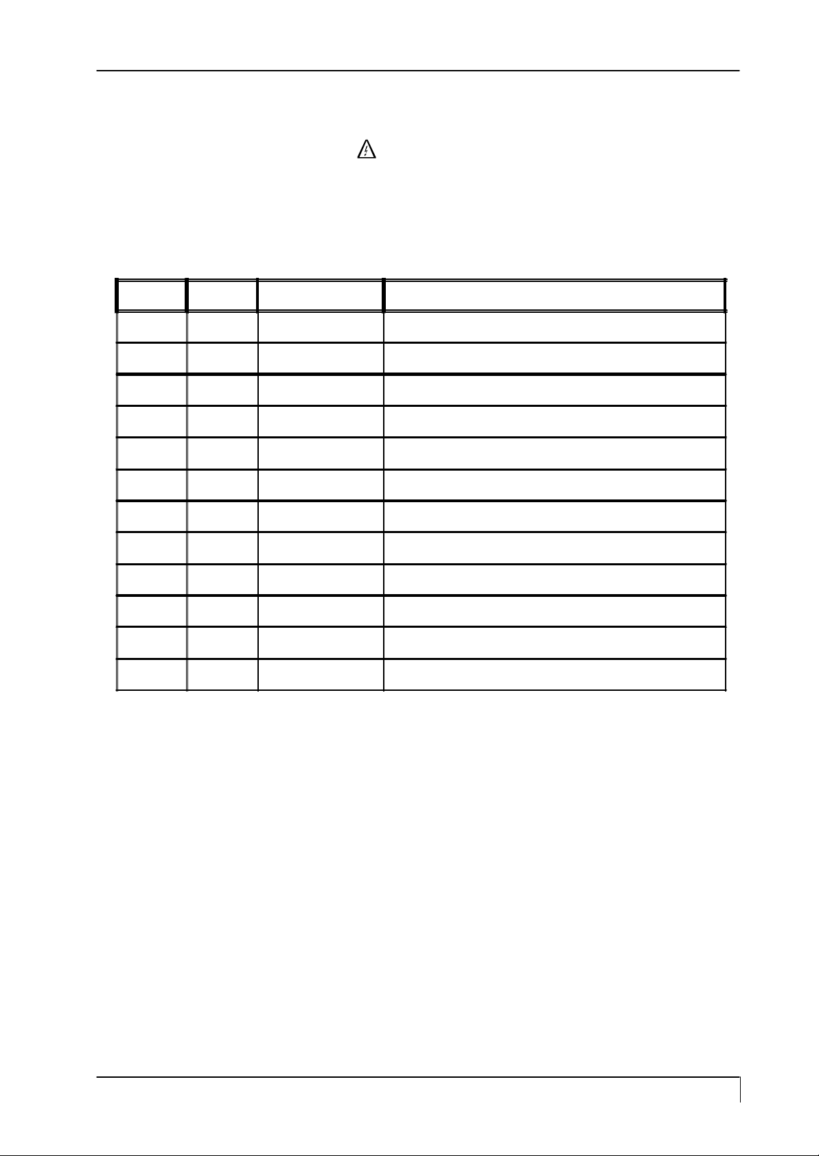
No. Location Part Number Description
1 *** I300 6447000406 IC MASCOT II CONTROLLER 160P PQFP
2 * I301 6447000506 IC VITESSEI 100P QFP
3 * I310 6446008108 IC NC7SZ04M5X SOT-23-5
4 ** I304 6448016508 IC EEPROM-24LC16B/SN SOP-8
5 ** I301 6447000506 IC ASIC-VITESSE2-100P-QFP
6 ** I307 6442001978 IC LM358DR 8P SOP
7 * I308 6442023326 IC AIC1084-33CM 3P T0263
8 *** Q300 6442007208 TR NPN SST2222A SOT-23
9 ** Q302 6427002508 FET-P-CHNL SI2305D3 SOT-2-3
10 *** Q303 6442007308 TR NPN SST3904 SOT-23
11 *** I001 6442023100 IC LINEAR-TDA7496L PDIP
12 * I303 6448018900 IC CPU SM89516C25J PLCC44P
Recom m end ed Spare Parts List Page 1
 Loading...