

Acer AL1917X Schematic

Acer Service Manual
Service Manual
LCD Monitor Acer
AL1917x
0
1
Service Manual Versions and Revision
No. Version Release Date Revision
1
1.0
2005/08/20
Initial Release
Copyright
Copyright 2005 InnoLux Tech. Corp. Ltd
All Rights Reserved
This manual may not, in whole or in part, be copied, Photocopied, reproduced, translated, or converted to any
electronic or machine readable form without prior written permission of InnoLux Tech. Corp. Ltd.
Acer AL1917 Service Manual
1

Acer Service Manual
Table of Contents
CHAPTER 1- PRECAUTIONS & SAFETY NOTICES ..................................................................................................................... 3
1. SAFETY PRECAUTIONS ................................................................................................................................................. 3
2. PRODUCT SAFETY NOTICE........................................................................................................................................... 3
3. SERVICE NOTES............................................................................................................................................................... 3
CHAPTER 2- SERVICE TOOLS & EQUIPMENT REQUIRED ..................................................................................................... 4
CHAPTER 3- CIRCUIT THEORY ...................................................................................................................................................... 5
1. BLOCK DIAGRAM .............................................................................................................................. 錯誤! 尚未定義書籤。
2. INTERFACE BOARD DIAGRAM ........................................................................................................................................... 5
3. ELECTRONIC CIRCUIT THEORY ............................................................................................................................................... 6
4. INVERTER CIRCUIT.............................................................................................................................錯誤! 尚未定義書籤。
CHAPTER 4- DISASSEMBLY & ASSEMBLY ................................................................................................................................... 9
1. EXPLODED DIAGRAM ............................................................................................................................................................. 9
2. DISASSEMBLY BLOCK ........................................................................................................................................................... 10
3. ASSEMBLY BLOCK ................................................................................................................................................................ 11
CHAPTER 5- TEST AND ADJUSTMENT........................................................................................................................................ 12
1. GENERAL POINTS............................................................................................................................................................. 12
2. INPUT SIGNAL.................................................................................................................................................................. 13
3. FUNCTION CHECK........................................................................................................................................................... 14
4. DISPLAY CHECK............................................................................................................................................................... 15
5. PICTURE CHECK............................................................................................................................................................... 16
6. AUDIO CHECK................................................................................................................................................................... 18
CHAPTER 6- TROUBLE SHOOTING.............................................................................................................................................. 19
1. NO POWER & LED OFF ..............................................................................................................19 錯誤! 尚未定義書籤。
UNSTABLE POWER ................................................................................................................................................................ 20
2.
3. NO RASTER ........................................................................................................................................................................... 21
4. BLACK SCREEN ..................................................................................................................................................................... 22
5. BAD SCREEN......................................................................................................................................................................... 23
6. WHITE SCREEN ..................................................................................................................................................................... 24
ATTACHMENT 1- BILL OF MATERIAL......................................................................................................................................... 25
ATTACHMENT 2- SCHEMATIC....................................................................................................................................................... 34
ATTACHMENT 3- PCB LAYOUT ..................................................................................................................................................... 44
2

Acer Service Manual
Chapter 1- PRECAUTIONS & SAFETY NOTICES
1. SAFETY PRECAUTIONS
This monitor is manufactured and tested on a ground principle that a user’s safety comes first.
However, improper used or installation may cause damage to the monitor as well as to the user.
WARNINGS:
This monitor should be operated only at the correct power sources indicated on the label on the rear
of the monitor. If you’re unsure of the power supply in you residence, consult your local dealer or
Power Company.
Do not try to repair the monitor by yourself, as it contains no user-serviceable parts. This monitor
should only be repaired by a qualified technician.
Do not remove the monitor cabinet. There are high-voltage parts inside that may cause electric
shock to human bodies.
Stop using the monitor if the cabinet is damaged. Have it checked by a service technician.
Put your monitor only in a lean, cool, dry environment. If it gets wet, unplug the power cable
immediately and consult your closed dealer.
Always unplug the monitor before cleaning it. Clean the cabinet with a clean, dry cloth. Apply
non-ammonia based cleaner onto the cloth, not directly onto the class screen.
Do not place heavy objects on the monitor or power cord.
2. PRODUCT SAFETY NOTICE
Many electrical and mechanical parts in this chassis have special safety visual inspections and the
protection afforded by them cannot necessarily be obtained by using replacement components rated
for higher voltage, wattage, etc. Before replacing any of these components read the parts list in this
manual carefully. The use of substitute replacement parts, which do not have the same safety
characteristics as specified in the parts list, may create shock, fire, or other hazards.
3. SERVICE NOTES
When replacing parts or circuit boards, clamp the lead wires around terminals before soldering.
Keep wires away from high voltage, high temperature components and sharp edges.
Keep wires in their original position so as to reduce interference.
Adjustment of this product please refers to the user’ manual.
3

Acer Service Manual
Chapter 2- SERVICE TOOLS & EQUIPMENT REQUIRED
1. SIGNAL GENERATOR
2. MULTIMETER
3. SCREW DRIVER
4. OSCILLOSCOPE
5. Soldering IRON
6. SOLDER
7. VGA Cable (15pins point to point)
8. Color Analyzer
9. Myson412 ISP Board
10. EDID Board
11. EDID program file
4
Acer Service Manual
Chapter 3- CIRCUIT THEORY
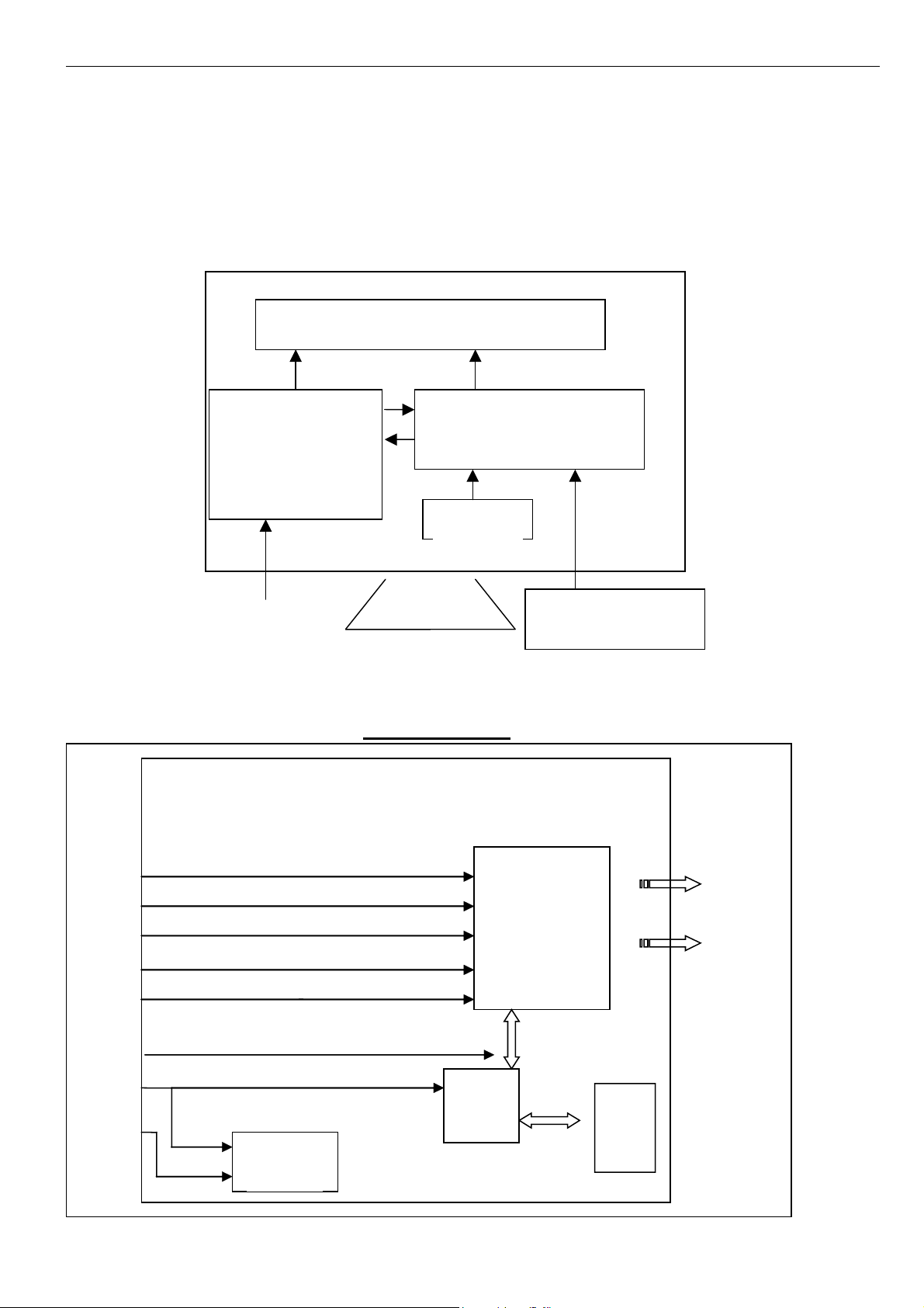
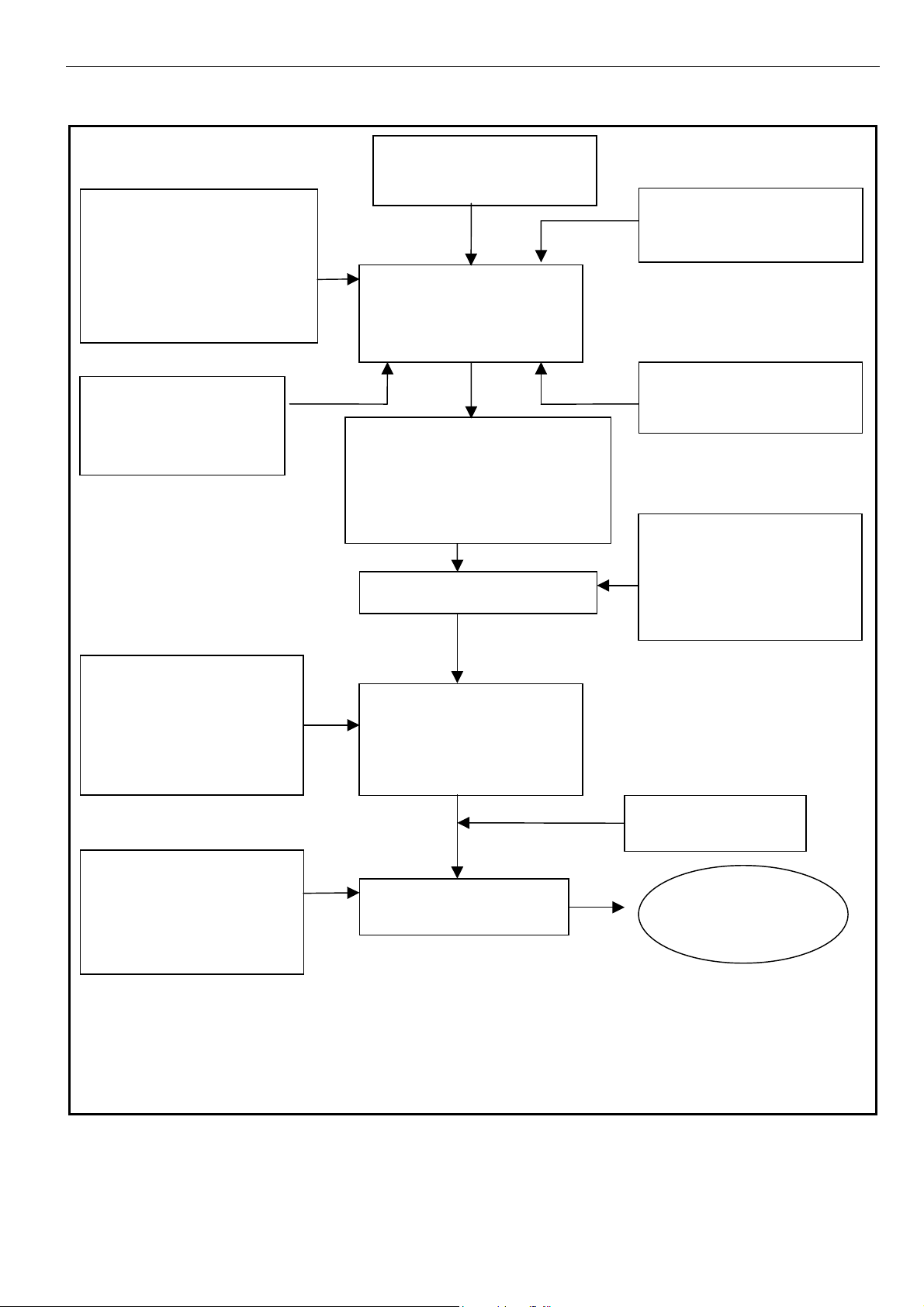
1. Monitor Block Diagram
The LCD Monitor contains an interface board, and inverter/power/Audio board, keypad board and flat
panel. In Inverter/power/Audio board, power section supplies +14V & +5V for Inverter/Audio and
Interface board used. The inverter section drives the backlight of panel and the DC-DC conversion. The
Audio section drives speaker (2 x1W).
Flat panel (LVDS interface) and CCFL
Inverter/Power/Audio BD
(Including AC/DC Power
Supply , Inverter and
Audio)
AC input
Range 100V~240V
2. Interface BOARD DIAGRAM
Interface Board
Interface Board (VGA input)
Keypad BD
Host computer
(VGA signal input and DDC)
Red
Green
Blue
A/D
&
Scaling
&
Vsync
OSD
Hsync
SCL
MCU
EEPROM
SDA
DDC
5
To
LCD
module

Acer Service Manual
3. Electronic Circuit Theory
3.1 Switching Mode Power Supply
3.1.1 AC Current Input Circuit
P801 is a connector for connecting AC Power. F801 is a fuse to protect all the circuit. AC input
voltage is from 90v to 264V. R820 and R821 joined between two inputting main circuit to prevent
man from shock. L801 is used to clear up low frequency wave. C801 and C806 are used to discharge
the waves that L801 produced. High frequency waves are damped by C801 and C806. D801 is a
rectifier which composed of 4 build-in diodes, it inverts AC to DC.
3.1.2 High Voltage to Low Voltage Control Circuit
C805 is used to smooth the wave from rectifier. IC802 is a highly integrated PWM controller
which build-in power MOSFET. When rectified DC high voltage is applied to the DRAIN pin during
start-up, the MOSFET is initially off, and the CONTROL pin capacitor is charged through a switched
high voltage current source connected internally between the DRAIN and CONTROL pins. When the
CONTROL pin voltage Vc reaches approximately 5.8V, the control circuitry is activated and the
soft-start begins. The soft-start circuit gradually increases the duty cycle of the MOSFET from zero to
the maximum value over approximately 10ms. If no external feedback/supply current is fed into the
CONTROL pin by the end of the soft-start, the high voltage current source is turned off and the
CONTROL pin will start discharging in response to the supply current drawn by the control circuitry.
Resistor R803, R807, R824 and R825 are for line over voltage shutdown(OV) and line
under-voltage detection(UV).
Resistors R801, R805, R822, R823 are for external current limit adjustment. And used to reduce
the current limit externally to a value close to the operating peak current of primary about 1.35A. The
mean is power will protected when the primary current over about 1.35A.
When PWM is turned off, the main current flow will be consumed through D804, and ZD802,
This will prevent MOSFET which built-in IC802 from being damaged under large current impulse and
voltage spike.
D806 and C815 to provide internal Auxiliary current to CONTROL pin during normal operation.
Otherwise, error amplifier and feedback current input the CONTROL pin for duty cycle control.
3.1.3 DC_5V and DC_14V Output Circuit
For DC 5V, D805 is used to rectify the inducted current. R806 and C811 are used to store energy
when current is reversed. The parts including C814, C814, C822, C821, B801 and L803 are used to
smooth the current waves.
For DC 14V, D803 is used to rectify the inducted current. R802 and C802 are used to store
energy when current is reversed. The parts including C808, C810 and L802 are used to smooth the
current waves.
3.1.4 Feedback and OVP Protect Circuit
Pin R of IC803 is supplied 2.5-v stable voltage. It connects to 5V and 14V output through R811,
R810 and R818. R811, R810 and R818 are output sampling resistor. When the sampling voltage more
than 2.5V or less than 2.5V, current of FB IC802 will change, this can change the voltage from T801.
For 5VDC output OVP, ZD803 is a Zener Diode, when 5 voltage up to 5.6V, the zener current
cause R819 voltage to ground is up to 0.7V, Q801 being triggered and OVP working. For 14VDC
output OVP, ZD804 is a Zener Diode, when 14 voltage up to 18V, the Zener current cause R819
voltage to groung is up to 0.7V, Q801 being triggered and OVP working. The current of potential is
used to make build-in diode light. Current of FB to IC802 will be changed, this can change the voltage
from T801.
Q802, R827, R828 and ZD801 make up of dummy loading circuit. For start-up sequence, during
5V output take place high loading first, this dummy loading circuit operated to insure 14V not be
increased.
3.2 I/F Board Circuit
3.2.1 RGB CAPTURE
- Signal RED,GREEN,BLUE input through CN102 #1,#2,#3, Stop DC via C117, C119 and C121,
and then enter into U104 (RTD2023L) analog input terminal #7,#9,#12, and then RTD2023 deals
6

Acer Service Manual
with signal internally. TVS101, TVS102, TVS103 are ESD protector to prevent U104 from ESD.
- Signal DDC_SCL (series clock) inputs via CN102#15, and then passes through ZD102 Zener for
ESD protection, goes into EDID EEPROM IC U103 #6.
- Signal DDC_SDA (series data) inputs via CN102#12, and then passes through ZD105 Zener for
ESD protection, goes into EDID EEPROM IC U103 #5.
- Signal TTL vertical sync. (Vsync) inputs via CN102 #14, and then clamped by ZD103 Zener,
passes through R124, and then goes into IC U104 (RTD2023L) #4.
- Signal TTL horizontal sync. (Hsync) inputs via CN102 #13, and then clamped byZD104 Zener,
passes through R125,R126, and then goes into IC U104 (RTD2023L) #5.
- CN102#5 is defined as cable detect pin, this detector realize passes through R152 Pull hight, go
into U105#9.
- U103 +5V is supplied by PC via CN102#9, or supplied by Monitor self via D101.
- U103 is an EEPROM IC which is memory and EDID data saved in it.
3.2.2 Buttons Control
- Button “Power” on right side bezel connects to U105 (MTV512) #48 through R177, via
CN104#4.
- Button “UP” “DOWN ““MENU” “AUTO” on right side bezel connects to U105 (MTV512)
#11,#12,#47,#46 through R175,R173,R172,R176,via CN104 #6, #7, #8, #5.
- U106 is an EEPROM IC which memory factory setting and save the value adjusted by user.
- SCL on U106 #6 and SDA on U106 #5 flow into U105 (MTV512) #37, #38.
- LED Indicator on Front Bezel
a. When press button “power”, U105 (MTV512) #1 sends out high potential, via R174, flow to
CN104 #2 on keypad, LED Blue ON.
b. When in “Suspend” mode, U105 (MTV512) #2 sends out a high potential, via R178, flows to
CN104 #1 on keypad, LED Amber ON.
3.2.3 Realtek CHIP U104 (RTD2023L)
- U104 (RTD2023L) #21~#30 output 8 bit even LVDS digital data to panel control circuit through
CN103.
- U104 (RTD2023L) #31~#40 output 8 bit odd LVDS digital data to panel control circuit through
CN103.
- U104 (RTD2023L) #15 outputs Brightness “PWM” signals to control CCFL brightness.
Please refer to RTD2023L Pin Assignments table in page
3.2.4 Myson chip U105(MTV512)
- U105 (MTV512) #39 output PPWR ”H” potential to make Q103 conducted, and then make Q101
conducted, +5V flow to CN103#1~#3 as Panel VDD .
- U105 (MTV512) #40 output CCFL_ON/OFF ”H” potential to control Inverter on/off.
- TCLK by Crystal 24MHz input to U105 (MTV512) #15,#16.
3.2.4 Regulator Circuit
- +5V is from switching mode power supply for Panel used.
- +3.3V generates from +5V through C101 and C103 filtering and U101 which is output +3.3V
LDO for U103, U104 and U105 used.
- +1.8V generates from +5V through C101 and C103 filtering and U102 which is output +1.8V
LDO, for U104 used.
3.2.5 Audio circuit
- Audio Signal R,L,GND input through P701,#2,#5,#1, Stop DC via C711, C712, and then enter
into U701 (TDA7496L) analog input terminal #4,#9.
- U701 (TDA7496L) #14,#17 output R,L audio data to Speaker through CN701.
- U105 (MTV512) #14 output MUTE “H” potential to control U701on/off.
- U105 (MTV) #45 outputs Volume “PWM” signals to control U701 Volume.
7

Acer Service Manual
4. Inverter circuit
4.1 Low voltage to high voltage circuit
14VDC provides the power for IC501 through F501; the control signals Brightness and ON/OFF
come from I/F board. ON/OFF signal connect to pin8 of IC501 and makes IC501 enable. Brightness
signal connect to pin7 of IC501 and regulates the panel brightness, R526, D515, R529, C505 make up a
network of delaying time circuit and R523, R524 make up a divided voltage network, C504 is used to
dump noise. The operation frequency is determined by the external Resistor R522 and capacitor C529
connected to pin5 of IC501. BURST MODE dimming pulse frequency and duty is regulated by I/F
board. C503 is used for soft start and compensation, C502, C528 are used for dump noise.
The output drives, include NDR4, NDRV2, PDRV3, PDRV1 (pins1, 3, 15, 16 respectively) output
square pulses to drive MOSFET U501, U502, and each of U501, U502 is consist of a N channel
MOSFET and a P channel MOSFET. U501 and U502 work as full-bridge topology, it is high efficient,
zero voltage switching.
During start up, VSEN (pin9) senses the voltage at the transformer secondary. When VSEN reaches
3.0V, the output voltage is regulated. If no current is sensed approximately 1.5 seconds IC501 shunt off.
The current flowing through CCFL is sensed and regulated through sense resistor R509, R511. The
feedback voltage through R506, R507, C508 connected to Pin11 (ISEN), then compared with a
reference voltage (1.5V) via a current amplifier, resulting in PWM drive outputs to full-bridge switches.
4.2 Protection circuit
Over Voltage Protection: R501and R502 are connected in high voltage output connector, the
divided AC voltage is inverted DC voltage through D508, R505 and C507are used to rectify wave &
dump noise. Then the voltage signal reaches Pin9 VSEN of IC501, when the voltage changes, build-in
PWM of IC501 will adjust output voltage.
Open Lamp Protection: In normal operation, the resistors R510, R511, R512, R509 are sensed a
high level AC voltage, the AC signal OP1 invert DC voltage through D509, R515, C533, and the high
level DC voltage reaches the gate pin of Q502, similarly, the gate pin of Q503, Q504, Q505 has high
level DC voltage. So the gate pin of Q501 has a low level voltage, and the IC501 is normal operation.
Once one of signal OP1, OP2, OP3, and OP4 is low, the voltages of Q501 gate pin is high level, and
make the voltage of ISEN low level, the IC501 will be shunt down.
8
Acer Service Manual
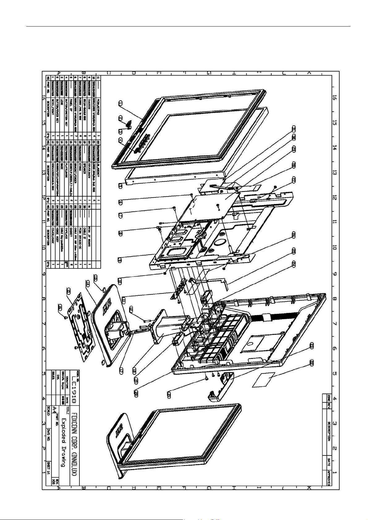
Chapter 4- Disassembly & Assembly
1. Exploded Diagram
9
Acer Service Manual
2. Disassembly Block
LE 1918
LCD Monitor
ASSY, BASE
BASE*1
RUBBER FOOT *4
GASKET*1
PLATE,BASE*1
T4*6,Zn, ROHS *2
HINGE COVER*1
BRACKET FINGER *1
HINGE *1
STAND
M4*18,Zn ROHS *3
ASSY STAND
M4*6,Black Zn,NL ROHS *6
ASSY FRONT BEZEL
BACK COVER
SCREW T4*8, Zn ROHS *2
SPEAKER*1
FRONT BEZEL *1
FUNCTION KEY *1
POWER BUTTON *1
LED LENS
CHASSIS *1
PCBA I/F BOARD *1
PCBA INV.&DC-DC *1
HRN ASS'Y 8P
M3*6,Zn ROHS *7
GASKET*1
ASSY PANEL UNIT
M3*4,Zn ROHS *4
CABLE 30P FFC
BOLT,#4-40x11.8,Ni ROHS
Note:
The DIS assembly direction please following direction of arrowhead
PANEL INNOLUX
MT190EN02_V0
10
Acer Service Manual
3. Assembly Block
PCBA INV.&DC-DC *1
PCBA I/F BOARD *1
CABLE 30 PIN FFC
M3*6,Zn ROHS *1
BOLT,#4-40x11.8,Ni ROHS
*2
GASKET*1
KEY PAD*1
HRN ASS'Y 8P
M3*6,Zn ROHS *2
M3*6,Zn ROHS *4
ASSY PANEL*1
M3*4,Zn ROHS *4
BACK COVER*1
SPEAKER*1
SCREW T4*8, Zn ROHS *2
TAPE ACE *2
ASSY BEZEL*1
PANEL INNOLUX
MT190EN02_V0
CHASSIS *1
BEZEL*1
BUTTON,POWER KEY*1
BUTTON,FUNCTION*1
LENS*1
STAND*1
HINGE*1
BRACKET FINGER*1
M4*18,Zn ROHS *3
BASE*1
RUBBER*4
GASKET*1
PLATE,BASE*1
T4*6,Zn, ROHS *2
ASSY STAND*1
M4*6,Black Zn,NL ROHS *6
ASSY BASE*1
HINGE COVER*1
LE 1918
LCD Monitor
11
Acer Service Manual
R
Chapter 5- TEST AND ADJUSTMENT
1. GENERAL POINTS
1.1 Test Equipment or Tool
1.1.1 Test pattern generator: PC or video pattern generator (Chroma-2326/2160/2130)
1.1.2 Color analyzer: Chroma-7120
1.1.3 Power meter: AC Source Chroma-6408
1.1.4 Electrical safety tester: Chroma (Zentech) 9032A
1.1.5 Stereo source: Music or signal generator input
1.1.6 Auto shock fixture
1.1.7 Temperature and humidity sensor
1.1.8 DDC interface card and EDID file
1.2 Preset Test Pattern
1.2.1 Crosshatch (General-1)
1.2.2 Gray Bar (16 & 32 levels)
1.2.3 Full White
1.2.4 Aging (Burn-in) Pattern: Full Red, Green, Blue, White, and Black
1.3 AC input
All measurements mentioned hereafter are carried out at a normal mains voltage (90 - 264 VAC for the
model with full range power supply, unless otherwise stated)
1.4 Observation Distance
1.4.1 Observation distance from eyes to panel is defined as 50cm
1.4.2 Visual distance from instrument to panel is defined as 20cm
1.5 Key Function Description
1.5.1 Control buttons on the front bezel
CONTROL
KEY
[AUTO]
[MENU]
[►], [◄]
[POWER] Power on or power off the monitor
A. When OSD un-displays, press [AUTO] to perform auto-adjustment
B. When OSD displays, press [AUTO] to return to previous level menu
A. When OSD isn’t shown on screen, press [MENU] to enter OSD interface
B. When OSD displays, press [MENU] to perform function of menu icon that is
highlight or enter next level menu
A. When “MENU OSD” displays, press these keys to change the contents of an
adjustment item, or change an adjustment value
B. When “MENU OSD” un-displays, press [►],adjust volume high;
press [◄]adjust volume low
KEYS FUNCTION
1.5.2 Hot Key Operation
HOT KEY OPERATION
FUNCTION
AUTO ◄ ► MENU POWE
Press [AUTO] & [MENU] at the same
FACTORY
MODE
● ● ON
12
time, and then press [POWER] for DC
power on. OSD menu will be shown
with “F” on the left top. Select “F” for
DESCRIPTION
Acer Service Manual
1.6 Burn-in (Aging) Pattern
1.6.1 Burn-in patterns are: full Red, Green, Blue, White and Black
1.6.2 Stop burn-in pattern by providing with video signal from D-sub connector
1.6.3 Enter or exit burn-in mode by setting “burn-in” to be “on” or “off” in the factory mode
1.7 Warm Up
All test units have to be done warm up after at least 2 hours in a room with temperature of 40±5°C.
(Except particular requirement)
2. INPUT SIGNAL
2.1 Video Signal Input
2.1.1 VESA Analog
The video input consists of red, green, and blue signals. The video signals are analog levels, where
0V corresponds to black and 700mV is the maximum signal amplitude. Input impedance of video
pins is 75 ohm ±1%.
Sync signal input
The capability of sync signal inputs shall include separate sync. Input impedance: 2k2 ohms the
signals are defined as follow:
Separate sync TTL level, Positive/Negative
2.1.2 Input signal mode
PRESET TEST MODE TIMING
Resolution H-Freq. (kHz) V-Fre q. ( Hz) Dot Clock (MHz) Mode
31.5 60.0 25.175
640 x 480
800 x 600
1024 x 768
1280 x 1024
640 x 350 31.5 70.0 25.175
720 x 400 31.5 70.0 28.322
832 x 624 49.7 74.6 57.283
1024 x 768
37.9 72.0 31.500
37.5 75.0 31.500
35.1 56.0 36.000
37.9 60.0 40.000
48.1 72.0 50.000
46.9 75.0 49.500
48.4 60.0 65.000
56.5 70.0 75.000
60.0 75.0 78.750
64.0 60.0 108.000
80.0 75.0 135.000
60.2 75.0 80.000
48.8 60.0 64.000
VESA
IBM-AT
Compatible
machine
PC-9800 series
US/IBM Text
Power Macintosh
series
2.1.3 VGA signal cable
15 pin D-sub VGA connector of signal cable.
2.1.4 Interface
Analog signal: The input signals are applied to display through D-sub cable.
Length: 1.8 m +/- 50 mm (fixed)
Connector type: D-sub male.
With DDC_2B pin assignments.
13
 Loading...